EP2993965A1 - Flexible printed circuit board and touch panel including the same - Google Patents
Flexible printed circuit board and touch panel including the same Download PDFInfo
- Publication number
- EP2993965A1 EP2993965A1 EP14192956.2A EP14192956A EP2993965A1 EP 2993965 A1 EP2993965 A1 EP 2993965A1 EP 14192956 A EP14192956 A EP 14192956A EP 2993965 A1 EP2993965 A1 EP 2993965A1
- Authority
- EP
- European Patent Office
- Prior art keywords
- fpcb
- touch
- bonding portion
- portions
- pads
- Prior art date
- Legal status (The legal status is an assumption and is not a legal conclusion. Google has not performed a legal analysis and makes no representation as to the accuracy of the status listed.)
- Granted
Links
Images

Classifications
-
- H—ELECTRICITY
- H05—ELECTRIC TECHNIQUES NOT OTHERWISE PROVIDED FOR
- H05K—PRINTED CIRCUITS; CASINGS OR CONSTRUCTIONAL DETAILS OF ELECTRIC APPARATUS; MANUFACTURE OF ASSEMBLAGES OF ELECTRICAL COMPONENTS
- H05K1/00—Printed circuits
- H05K1/02—Details
- H05K1/11—Printed elements for providing electric connections to or between printed circuits
-
- G—PHYSICS
- G06—COMPUTING OR CALCULATING; COUNTING
- G06F—ELECTRIC DIGITAL DATA PROCESSING
- G06F3/00—Input arrangements for transferring data to be processed into a form capable of being handled by the computer; Output arrangements for transferring data from processing unit to output unit, e.g. interface arrangements
- G06F3/01—Input arrangements or combined input and output arrangements for interaction between user and computer
- G06F3/03—Arrangements for converting the position or the displacement of a member into a coded form
- G06F3/041—Digitisers, e.g. for touch screens or touch pads, characterised by the transducing means
- G06F3/0416—Control or interface arrangements specially adapted for digitisers
- G06F3/04164—Connections between sensors and controllers, e.g. routing lines between electrodes and connection pads
-
- G—PHYSICS
- G06—COMPUTING OR CALCULATING; COUNTING
- G06F—ELECTRIC DIGITAL DATA PROCESSING
- G06F3/00—Input arrangements for transferring data to be processed into a form capable of being handled by the computer; Output arrangements for transferring data from processing unit to output unit, e.g. interface arrangements
- G06F3/01—Input arrangements or combined input and output arrangements for interaction between user and computer
- G06F3/03—Arrangements for converting the position or the displacement of a member into a coded form
- G06F3/033—Pointing devices displaced or positioned by the user, e.g. mice, trackballs, pens or joysticks; Accessories therefor
-
- G—PHYSICS
- G06—COMPUTING OR CALCULATING; COUNTING
- G06F—ELECTRIC DIGITAL DATA PROCESSING
- G06F3/00—Input arrangements for transferring data to be processed into a form capable of being handled by the computer; Output arrangements for transferring data from processing unit to output unit, e.g. interface arrangements
- G06F3/01—Input arrangements or combined input and output arrangements for interaction between user and computer
- G06F3/03—Arrangements for converting the position or the displacement of a member into a coded form
- G06F3/041—Digitisers, e.g. for touch screens or touch pads, characterised by the transducing means
-
- H—ELECTRICITY
- H05—ELECTRIC TECHNIQUES NOT OTHERWISE PROVIDED FOR
- H05K—PRINTED CIRCUITS; CASINGS OR CONSTRUCTIONAL DETAILS OF ELECTRIC APPARATUS; MANUFACTURE OF ASSEMBLAGES OF ELECTRICAL COMPONENTS
- H05K1/00—Printed circuits
- H05K1/02—Details
- H05K1/0277—Bendability or stretchability details
- H05K1/028—Bending or folding regions of flexible printed circuits
- H05K1/0281—Reinforcement details thereof
-
- H—ELECTRICITY
- H05—ELECTRIC TECHNIQUES NOT OTHERWISE PROVIDED FOR
- H05K—PRINTED CIRCUITS; CASINGS OR CONSTRUCTIONAL DETAILS OF ELECTRIC APPARATUS; MANUFACTURE OF ASSEMBLAGES OF ELECTRICAL COMPONENTS
- H05K3/00—Apparatus or processes for manufacturing printed circuits
- H05K3/36—Assembling printed circuits with other printed circuits
- H05K3/361—Assembling flexible printed circuits with other printed circuits
-
- G—PHYSICS
- G06—COMPUTING OR CALCULATING; COUNTING
- G06F—ELECTRIC DIGITAL DATA PROCESSING
- G06F2203/00—Indexing scheme relating to G06F3/00 - G06F3/048
- G06F2203/041—Indexing scheme relating to G06F3/041 - G06F3/045
- G06F2203/04102—Flexible digitiser, i.e. constructional details for allowing the whole digitising part of a device to be flexed or rolled like a sheet of paper
-
- G—PHYSICS
- G06—COMPUTING OR CALCULATING; COUNTING
- G06F—ELECTRIC DIGITAL DATA PROCESSING
- G06F3/00—Input arrangements for transferring data to be processed into a form capable of being handled by the computer; Output arrangements for transferring data from processing unit to output unit, e.g. interface arrangements
- G06F3/01—Input arrangements or combined input and output arrangements for interaction between user and computer
- G06F3/03—Arrangements for converting the position or the displacement of a member into a coded form
- G06F3/041—Digitisers, e.g. for touch screens or touch pads, characterised by the transducing means
- G06F3/044—Digitisers, e.g. for touch screens or touch pads, characterised by the transducing means by capacitive means
- G06F3/0446—Digitisers, e.g. for touch screens or touch pads, characterised by the transducing means by capacitive means using a grid-like structure of electrodes in at least two directions, e.g. using row and column electrodes
-
- H—ELECTRICITY
- H05—ELECTRIC TECHNIQUES NOT OTHERWISE PROVIDED FOR
- H05K—PRINTED CIRCUITS; CASINGS OR CONSTRUCTIONAL DETAILS OF ELECTRIC APPARATUS; MANUFACTURE OF ASSEMBLAGES OF ELECTRICAL COMPONENTS
- H05K1/00—Printed circuits
- H05K1/02—Details
- H05K1/11—Printed elements for providing electric connections to or between printed circuits
- H05K1/118—Printed elements for providing electric connections to or between printed circuits specially for flexible printed circuits, e.g. using folded portions
-
- H—ELECTRICITY
- H05—ELECTRIC TECHNIQUES NOT OTHERWISE PROVIDED FOR
- H05K—PRINTED CIRCUITS; CASINGS OR CONSTRUCTIONAL DETAILS OF ELECTRIC APPARATUS; MANUFACTURE OF ASSEMBLAGES OF ELECTRICAL COMPONENTS
- H05K1/00—Printed circuits
- H05K1/02—Details
- H05K1/14—Structural association of two or more printed circuits
- H05K1/148—Arrangements of two or more hingeably connected rigid printed circuit boards, i.e. connected by flexible means
-
- H—ELECTRICITY
- H05—ELECTRIC TECHNIQUES NOT OTHERWISE PROVIDED FOR
- H05K—PRINTED CIRCUITS; CASINGS OR CONSTRUCTIONAL DETAILS OF ELECTRIC APPARATUS; MANUFACTURE OF ASSEMBLAGES OF ELECTRICAL COMPONENTS
- H05K2201/00—Indexing scheme relating to printed circuits covered by H05K1/00
- H05K2201/05—Flexible printed circuits [FPCs]
- H05K2201/052—Branched
-
- H—ELECTRICITY
- H05—ELECTRIC TECHNIQUES NOT OTHERWISE PROVIDED FOR
- H05K—PRINTED CIRCUITS; CASINGS OR CONSTRUCTIONAL DETAILS OF ELECTRIC APPARATUS; MANUFACTURE OF ASSEMBLAGES OF ELECTRICAL COMPONENTS
- H05K2201/00—Indexing scheme relating to printed circuits covered by H05K1/00
- H05K2201/05—Flexible printed circuits [FPCs]
- H05K2201/058—Direct connection between two or more FPCs or between flexible parts of rigid PCBs
-
- H—ELECTRICITY
- H05—ELECTRIC TECHNIQUES NOT OTHERWISE PROVIDED FOR
- H05K—PRINTED CIRCUITS; CASINGS OR CONSTRUCTIONAL DETAILS OF ELECTRIC APPARATUS; MANUFACTURE OF ASSEMBLAGES OF ELECTRICAL COMPONENTS
- H05K2201/00—Indexing scheme relating to printed circuits covered by H05K1/00
- H05K2201/09—Shape and layout
- H05K2201/09209—Shape and layout details of conductors
- H05K2201/09654—Shape and layout details of conductors covering at least two types of conductors provided for in H05K2201/09218 - H05K2201/095
- H05K2201/09781—Dummy conductors, i.e. not used for normal transport of current; Dummy electrodes of components
-
- H—ELECTRICITY
- H05—ELECTRIC TECHNIQUES NOT OTHERWISE PROVIDED FOR
- H05K—PRINTED CIRCUITS; CASINGS OR CONSTRUCTIONAL DETAILS OF ELECTRIC APPARATUS; MANUFACTURE OF ASSEMBLAGES OF ELECTRICAL COMPONENTS
- H05K2201/00—Indexing scheme relating to printed circuits covered by H05K1/00
- H05K2201/10—Details of components or other objects attached to or integrated in a printed circuit board
- H05K2201/10227—Other objects, e.g. metallic pieces
- H05K2201/1034—Edge terminals, i.e. separate pieces of metal attached to the edge of the printed circuit board [PCB]
-
- H—ELECTRICITY
- H05—ELECTRIC TECHNIQUES NOT OTHERWISE PROVIDED FOR
- H05K—PRINTED CIRCUITS; CASINGS OR CONSTRUCTIONAL DETAILS OF ELECTRIC APPARATUS; MANUFACTURE OF ASSEMBLAGES OF ELECTRICAL COMPONENTS
- H05K2201/00—Indexing scheme relating to printed circuits covered by H05K1/00
- H05K2201/10—Details of components or other objects attached to or integrated in a printed circuit board
- H05K2201/10227—Other objects, e.g. metallic pieces
- H05K2201/10356—Cables
-
- H—ELECTRICITY
- H05—ELECTRIC TECHNIQUES NOT OTHERWISE PROVIDED FOR
- H05K—PRINTED CIRCUITS; CASINGS OR CONSTRUCTIONAL DETAILS OF ELECTRIC APPARATUS; MANUFACTURE OF ASSEMBLAGES OF ELECTRICAL COMPONENTS
- H05K2201/00—Indexing scheme relating to printed circuits covered by H05K1/00
- H05K2201/20—Details of printed circuits not provided for in H05K2201/01 - H05K2201/10
- H05K2201/2009—Reinforced areas, e.g. for a specific part of a flexible printed circuit
Definitions
- This document relates to a flexible printed circuit board and a touch panel including the same, and more particularly, to a flexible printed circuit board having enhanced peeling force and a touch panel including the same.
- FPCBs Flexible printed circuit boards
- PCB printed circuit board
- bendable have advantages of enabling 3D wiring and reducing a size and weight. For this reason, recently, as electronic devices have been reduced in size and weight, FPCBs have been used in products whose service availability is limited due to a solid PCB or manual operation circuits or in various application fields requiring bending quality or space saving.
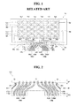
- FIG. 1 is a view illustrating a related art FPCB applied to a touch panel.
- a touch panel TS includes touch electrodes Tx1 to Tx4 and Rx1 to Rx6, touch routing wirings TW1 to TW4 and RW1 to RW6, and touch pads TP1 to TP4 and RP1 to RP6, and an FPCB includes bonding portions BP1 and BP2 and an FPCB wiring formation portion WP.
- the touch electrodes include a plurality of first touch electrodes Tx1 to Tx4 arranged to be parallel in a first direction such as a horizontal direction and a plurality of second touch electrodes Rx1 to Rx6 arranged to be parallel in a second direction such as a vertical direction intersecting the first direction.
- the touch routing wirings include first touch routing wirings TW1 to TW4 having one ends respectively connected to the plurality of first touch electrodes Tx1 to Tx4 and second touch routing wirings RW1 to RW6 having one ends respectively connected to the plurality of second touch electrodes Rx1 to Rx6.
- the touch pads include first touch pads TP1 to TP4 respectively connected to the other ends of the first touch routing wirings TW1 to TW4 and second touch pads RP1 to RP6 respectively connected to the other ends of the second touch routing wirings RW1 to RW6.
- the first bonding portion BP1 of the FPCB is a portion bonded to an end portion of the touch panel TS so as to be electrically in contact with the first and second touch pads TP1 to TP4 and RP1 to RP6, and the second bonding portion BP2 is a portion bonded to an external circuit (not shown).
- the FPCB wiring formation portion WP includes signal wirings FTW2, FTW4, FRW1 ⁇ FRW6, FTW2, FTW1, respectively connecting the first and second touch pads TP2, TP4, RP1 ⁇ RP6, TP2, TP1 of the touch panel TS to an external circuit.
- a touch electrode formation portion in which the touch electrodes Tx1 to Tx4 and Rx1 to Rx6 are disposed and the outermost portion of the FPCB are in proximity to each other in the bonding region of the FPCB and the touch panel TS.
- An embodiment of the present invention provides a flexible printed circuit board having enhanced peeling force sufficient not to be damaged with external force applied thereto.
- a flexible printed circuit board includes a first bonding portion and a second bonding portion respectively bonded to a first circuit unit and a second circuit unit.
- the first bonding portion may include a pad corresponding portion corresponding to pads of the first circuit unit and dummy portions outwardly extending from both end portions of the pad corresponding portion.
- An FPCB wiring formation portion may include FPCB wirings respectively connected to the pads and extending from the first bonding portion to the second bonding portion and concave portions respectively disposed to be adjacent to the dummy portions and having a curved surface.
- the FPCB wiring formation portion may further include reinforcing patterns independently disposed along regions in which the concave portions are disposed.
- a touch panel including a flexible printed circuit board includes: a touch panel including touch electrodes, touch routing wirings having one end portions respectively connected to the touch electrodes, and touch pads respectively connected to the other end portions of the touch routing wirings.
- the FPCB may include a bonding portion and an FPCB wiring formation portion.
- the bonding portion may include a pad corresponding portion corresponding to the touch pads of the touch panel and dummy portions outwardly extending from both ends portions of the pad corresponding portion.
- the FPCB wiring formation portion may include FPCB wirings respectively connected to the touch pads and arranged to extend to an end thereof and concave portions respectively disposed to be adjacent to the dummy portions and having a curved surface.
- the FPCB wiring formation portion may further include reinforcing patterns independently disposed along regions in which the concave portions are disposed.
- the first bonding portion includes the first and second dummy portions in addition to the pad corresponding portion, a bonded region can be increased by the first and second dummy portions.
- the region of the pad corresponding portion cannot be damaged.
- generation of a defective product due to damage to the FPCB can be prevented.
- the FPCB of an embodiment of the present invention since the first and second concave portions having a curved surface are disposed at both corner portions of the wiring formation portion adjacent to the first and second dummy portions, even though external impact is applied to the wiring formation portion, the impact is absorbed to the first and second concave portions, whereby the first bonding portion of the FPCB can be prevented from being torn by the external force, thus preventing generation of a defective product.
- the FPCB of an embodiment of the present invention since the first and second reinforcing patterns of the wiring formation portion are disposed along both lateral portions of the concave portions of the wiring formation portion and formed of a metal, rigidity of the FPCB can be reinforced. Thus, even though external impact is applied, the FPCB can be prevented from being damaged by the impact.
- a flexible printed circuit board including a first bonding portion and a second bonding portion configured to be bonded to a first circuit unit and a second circuit unit, respectively, the FPCB comprising: the first bonding portion including a pad corresponding portion corresponding to pads of the first circuit unit and dummy portions outwardly extending from both end portions of the pad corresponding portion; and an FPCB wiring formation portion including FPCB wirings configured to be respectively connected to the pads and extending from the first bonding portion to the second bonding portion and concave portions respectively disposed to be adjacent to the dummy portions and having a curved surface.
- FPCB flexible printed circuit board
- the FPCB wiring formation portion further includes reinforcing patterns independently disposed along regions in which the concave portions are disposed.
- Various embodiments also provide a touch panel including touch electrodes, touch routing wirings having one end portions respectively connected to the touch electrodes, and touch pads respectively connected to the other end portions of the touch routing wirings, the touch panel further comprising: the flexible printed circuit board (FPCB) including: the first bonding portion including the pad corresponding portion corresponding to the touch pads of the touch panel and the dummy portions outwardly extending from both ends portions of the pad corresponding portion, and the FPCB wiring formation portion including the FPCB wirings respectively connected to the touch pads and arranged to extend from the first bonding portion to the second bonding portion, and the concave portions respectively disposed to be adjacent to the dummy portions and having the curved surface.
- FPCB flexible printed circuit board
- FIG. 2 is a plan view illustrating an FPCB according to an embodiment of the present invention.
- the FPCB includes a first bonding portion BP1, an FPCB wiring formation portion WP, and a second bonding portion BP2, as connectors for electrically connecting separated first and second circuit devices.
- the first bonding portion BP1 is a portion disposed at one end portion of the FPCB and bonded to a pad region in which pads of the first circuit device are disposed.
- the first bonding portion BP1 includes a pad corresponding portion PC and first and second dummy portions D1 and D2 outwardly extending from both end portions of the pad corresponding portion PC, respectively.
- a region of the first bonding portion BP1 bonded with the first circuit device is increased by the first and second dummy portions D1 and D2.
- the region bonding the FPCB to the first circuit device is increased by the region corresponding to the first and second dummy portions D1 and D2, even though external force is applied from the left and right sides of the FPCB, the region of the pad corresponding portion PC is not damaged. Thus, generation of a defect product due to damage to the FPCB can be prevented.
- the FPCB wiring formation portion WP includes FPCB wirings FTW2, FTW4, FRW1 to FRW6, FTW3, FTW1 arranged from the pad corresponding portion PC of the first bonding portion BP1 to the second bonding portion to form an electrical path for connecting the first circuit device and the second circuit device.
- the FPCB wiring formation portion WP includes first and second concave portions CP1 and CP2 disposed to have a curved surface outwardly at both corner portions adjacent to the first and second dummy portions D1 and D2 of the first bonding portion BP1.
- first and second concave portions CP1 and CP2 having a curved surface are disposed at both corner portions of the FPCB wiring formation portion WP adjacent to the first and second dummy portions D1 and D2, even though impact is applied to the FPCB wiring formation portion WP from the outside, the impact is absorbed to the first and second concave portions CP1 and CP2, whereby the first bonding portion BPlof the FPCB is prevented from being torn due to external force, thus preventing generation of a defective product.
- the FPCB wiring formation portion WP may further include first and second reinforcing patterns RF1 and RF2 independently disposed on the regions of the first and second concave portions CP1 and CP2.
- the first and second reinforcing patterns RF1 and RF2 may extend to a portion spaced apart from the second bonding portion BP2 or may extend to reach the second bonding portion BP2, along both lateral portions of the FPCB wiring formation portion WP.
- the first and second reinforcing patterns RF1 and RF2 may be formed of a metal having excellent conductivity identical to that of the FPCB wirings FTW2, FTW4, FRW1 to FRW6, FTW3, FTW1, and electrically float from any other components, as well as the first and second circuit devices.
- first and second reinforcing patterns RF1 and RF2 of the FPCB wiring formation portion WP are formed of a metal and disposed along the both lateral portions of the FPCB wiring formation portion WP, rigidity of the FPCB can be reinforced. Thus, even though external impact is applied, the FPCB can be prevented from being damaged.
- FCPB FCPB according to an embodiment of the present invention
- FIG. 3 is a view schematically illustrating a state in which the flexible printed circuit board according to an embodiment of the present invention is applied to a touch panel.
- a touch panel TS including the FPCB includes touch electrodes Tx1 to Tx4 and Rx1 to Rx6, touch routing wirings TW1 to TW4 and RW1 to RW6, and touch pads TP1 to TP4 and RP1 to RP6.
- the touch electrodes include a plurality of first touch electrodes Tx1 to Tx4 arranged to be parallel in a first direction as a horizontal direction and a plurality of second touch electrodes Rx1 to Rx6 arranged to be parallel in a second direction as a vertical direction intersecting the first direction.
- the touch routing wirings include first touch routing wirings TW1 to TW4 having one ends respectively connected to the plurality of first touch electrodes Tx1 to Tx4 and second touch routing wirings RW1 to RW6 having one ends respectively connected to the plurality of second touch electrodes Rx1 to Rx6.
- the touch pads include first touch pads TP1 to TP4 respectively connected to the other ends of the first touch routing wirings TW1 to TW4 and second touch pads RP1 to RP6 respectively connected to the other ends of the second touch routing wirings RW1 to RW6.
- the first bonding portion BP1 of the FPCB is bonded to an end portion of the touch panel TS so as to be electrically in contact with the first and second touch pads TP1 to TP4 and RP1 to RP6.
- the pad corresponding portion PC of the first bonding portion BP1 may overlap the touch pads TP1 to TP4 and RP1 to RP6, and the first and second dummy portions D1 and D2 do not overlap any of the touch pads TP1 to TP4 and RP1 to RP6.
- the second bonding portion BP2 is a portion bonded to an external circuit (not shown).
- the FPCB wiring formation portion WP of the FPCB includes FPCB wirings FTW2, FTW4, FRW1 to FRW6, FTW2, FTW1 respectively connecting the first and second touch pads TP2, TP4, RP1 to RP6, TP2, TP1 of the touch panel TS to an external circuit.
- the FPCB wirings FTW2, FTW4, FRW1 to FRW6, FTW2, FTW1 are arranged to extend from the first bonding portion BP1 to the second bonding portion BP2.
- the FPCB wiring formation portion includes the first and second reinforcing portions together with the first and second concave portions, even though external impact is applied, the FPCB can be prevented from being damaged by the impact or the pad corresponding portion of the first bonding portion can be prevented from being torn off from the touch panel. Thus, defective touch driving due to damage to the FPCB can be prevented.
Landscapes
- Engineering & Computer Science (AREA)
- General Engineering & Computer Science (AREA)
- Theoretical Computer Science (AREA)
- Microelectronics & Electronic Packaging (AREA)
- Human Computer Interaction (AREA)
- Physics & Mathematics (AREA)
- General Physics & Mathematics (AREA)
- Manufacturing & Machinery (AREA)
- Computer Networks & Wireless Communication (AREA)
- Structure Of Printed Boards (AREA)
- Position Input By Displaying (AREA)
Abstract
Description
- This document relates to a flexible printed circuit board and a touch panel including the same, and more particularly, to a flexible printed circuit board having enhanced peeling force and a touch panel including the same.
- Flexible printed circuit boards (FPCBs), which are a type of printed circuit board (PCB) and are bendable, have advantages of enabling 3D wiring and reducing a size and weight. For this reason, recently, as electronic devices have been reduced in size and weight, FPCBs have been used in products whose service availability is limited due to a solid PCB or manual operation circuits or in various application fields requiring bending quality or space saving.
- Hereinafter, an application of a related art FPCB to a touch panel will be described in detail with reference to
FIG. 1. FIG. 1 is a view illustrating a related art FPCB applied to a touch panel. - Referring to
FIG. 1 , a touch panel TS includes touch electrodes Tx1 to Tx4 and Rx1 to Rx6, touch routing wirings TW1 to TW4 and RW1 to RW6, and touch pads TP1 to TP4 and RP1 to RP6, and an FPCB includes bonding portions BP1 and BP2 and an FPCB wiring formation portion WP. - The touch electrodes include a plurality of first touch electrodes Tx1 to Tx4 arranged to be parallel in a first direction such as a horizontal direction and a plurality of second touch electrodes Rx1 to Rx6 arranged to be parallel in a second direction such as a vertical direction intersecting the first direction.
- The touch routing wirings include first touch routing wirings TW1 to TW4 having one ends respectively connected to the plurality of first touch electrodes Tx1 to Tx4 and second touch routing wirings RW1 to RW6 having one ends respectively connected to the plurality of second touch electrodes Rx1 to Rx6.
- The touch pads include first touch pads TP1 to TP4 respectively connected to the other ends of the first touch routing wirings TW1 to TW4 and second touch pads RP1 to RP6 respectively connected to the other ends of the second touch routing wirings RW1 to RW6.
- The first bonding portion BP1 of the FPCB is a portion bonded to an end portion of the touch panel TS so as to be electrically in contact with the first and second touch pads TP1 to TP4 and RP1 to RP6, and the second bonding portion BP2 is a portion bonded to an external circuit (not shown). The FPCB wiring formation portion WP includes signal wirings FTW2, FTW4, FRW1∼FRW6, FTW2, FTW1, respectively connecting the first and second touch pads TP2, TP4, RP1∼RP6, TP2, TP1 of the touch panel TS to an external circuit.
- In the related art FPCB described above, when external force acts on an outer portion of the first bonding portion BP1, a bonding region may be detached or an outer portion of the FPCB may be damaged to result in a separation of the FPCB from the touch panel TS.
- Here, as the products tend to be reduced in size, a touch electrode formation portion in which the touch electrodes Tx1 to Tx4 and Rx1 to Rx6 are disposed and the outermost portion of the FPCB are in proximity to each other in the bonding region of the FPCB and the touch panel TS. Thus, even though only a portion of the first bonding portion BP1 of the FPCB is torn, defective touch driving may occur.
- An embodiment of the present invention provides a flexible printed circuit board having enhanced peeling force sufficient not to be damaged with external force applied thereto.
- In an aspect, a flexible printed circuit board (FPCB) includes a first bonding portion and a second bonding portion respectively bonded to a first circuit unit and a second circuit unit. The first bonding portion may include a pad corresponding portion corresponding to pads of the first circuit unit and dummy portions outwardly extending from both end portions of the pad corresponding portion. An FPCB wiring formation portion may include FPCB wirings respectively connected to the pads and extending from the first bonding portion to the second bonding portion and concave portions respectively disposed to be adjacent to the dummy portions and having a curved surface.
- In the foregoing configuration, the FPCB wiring formation portion may further include reinforcing patterns independently disposed along regions in which the concave portions are disposed.
- In another aspect, a touch panel including a flexible printed circuit board (FPCB) includes: a touch panel including touch electrodes, touch routing wirings having one end portions respectively connected to the touch electrodes, and touch pads respectively connected to the other end portions of the touch routing wirings. The FPCB may include a bonding portion and an FPCB wiring formation portion. The bonding portion may include a pad corresponding portion corresponding to the touch pads of the touch panel and dummy portions outwardly extending from both ends portions of the pad corresponding portion. The FPCB wiring formation portion may include FPCB wirings respectively connected to the touch pads and arranged to extend to an end thereof and concave portions respectively disposed to be adjacent to the dummy portions and having a curved surface.
- In the foregoing configuration, the FPCB wiring formation portion may further include reinforcing patterns independently disposed along regions in which the concave portions are disposed.
- According to the FPCB of an embodiment of the present invention, since the first bonding portion includes the first and second dummy portions in addition to the pad corresponding portion, a bonded region can be increased by the first and second dummy portions. Thus, even though external force is applied from the left and right sides of the FPCB, the region of the pad corresponding portion cannot be damaged. Thus, generation of a defective product due to damage to the FPCB can be prevented.
- Also, according to the FPCB of an embodiment of the present invention, since the first and second concave portions having a curved surface are disposed at both corner portions of the wiring formation portion adjacent to the first and second dummy portions, even though external impact is applied to the wiring formation portion, the impact is absorbed to the first and second concave portions, whereby the first bonding portion of the FPCB can be prevented from being torn by the external force, thus preventing generation of a defective product.
- Also, according to the FPCB of an embodiment of the present invention, since the first and second reinforcing patterns of the wiring formation portion are disposed along both lateral portions of the concave portions of the wiring formation portion and formed of a metal, rigidity of the FPCB can be reinforced. Thus, even though external impact is applied, the FPCB can be prevented from being damaged by the impact.
- Various embodiments provide a flexible printed circuit board (FPCB) including a first bonding portion and a second bonding portion configured to be bonded to a first circuit unit and a second circuit unit, respectively, the FPCB comprising: the first bonding portion including a pad corresponding portion corresponding to pads of the first circuit unit and dummy portions outwardly extending from both end portions of the pad corresponding portion; and an FPCB wiring formation portion including FPCB wirings configured to be respectively connected to the pads and extending from the first bonding portion to the second bonding portion and concave portions respectively disposed to be adjacent to the dummy portions and having a curved surface.
- In one or more embodiments, the FPCB wiring formation portion further includes reinforcing patterns independently disposed along regions in which the concave portions are disposed.
- Various embodiments also provide a touch panel including touch electrodes, touch routing wirings having one end portions respectively connected to the touch electrodes, and touch pads respectively connected to the other end portions of the touch routing wirings, the touch panel further comprising: the flexible printed circuit board (FPCB) including: the first bonding portion including the pad corresponding portion corresponding to the touch pads of the touch panel and the dummy portions outwardly extending from both ends portions of the pad corresponding portion, and the FPCB wiring formation portion including the FPCB wirings respectively connected to the touch pads and arranged to extend from the first bonding portion to the second bonding portion, and the concave portions respectively disposed to be adjacent to the dummy portions and having the curved surface.
- The accompanying drawings, which are included to provide a further understanding of the invention and are incorporated in and constitute a part of this specification, illustrate embodiments of the invention and together with the description serve to explain the principles of the invention. In the drawings:
-
FIG. 1 is a view illustrating a related art flexible printed circuit board applied to a touch panel; -
FIG. 2 is a plan view illustrating a flexible printed circuit board according to an embodiment of the present invention; and -
FIG. 3 is a view schematically illustrating a state in which the flexible printed circuit board according to an embodiment of the present invention is applied to a touch panel. - Hereinafter, embodiments of the present invention will be described in detail with reference to the accompanying drawings. Throughout the specification, the like reference numerals denote the substantially same elements. In describing the present invention, if a detailed explanation for a related known function or construction is considered to unnecessarily divert the gist of the present invention, such explanation will be omitted.
- A flexible printed circuit board (FPCB) according to an embodiment of the present invention will be described in detail with reference to
FIG. 2. FIG. 2 is a plan view illustrating an FPCB according to an embodiment of the present invention. - Referring to
FIG. 2 , the FPCB according to an embodiment of the present invention includes a first bonding portion BP1, an FPCB wiring formation portion WP, and a second bonding portion BP2, as connectors for electrically connecting separated first and second circuit devices. - The first bonding portion BP1 is a portion disposed at one end portion of the FPCB and bonded to a pad region in which pads of the first circuit device are disposed. The first bonding portion BP1 includes a pad corresponding portion PC and first and second dummy portions D1 and D2 outwardly extending from both end portions of the pad corresponding portion PC, respectively.
- A region of the first bonding portion BP1 bonded with the first circuit device is increased by the first and second dummy portions D1 and D2. Thus, since the region bonding the FPCB to the first circuit device is increased by the region corresponding to the first and second dummy portions D1 and D2, even though external force is applied from the left and right sides of the FPCB, the region of the pad corresponding portion PC is not damaged. Thus, generation of a defect product due to damage to the FPCB can be prevented.
- The FPCB wiring formation portion WP includes FPCB wirings FTW2, FTW4, FRW1 to FRW6, FTW3, FTW1 arranged from the pad corresponding portion PC of the first bonding portion BP1 to the second bonding portion to form an electrical path for connecting the first circuit device and the second circuit device.
- The FPCB wiring formation portion WP includes first and second concave portions CP1 and CP2 disposed to have a curved surface outwardly at both corner portions adjacent to the first and second dummy portions D1 and D2 of the first bonding portion BP1.
- Since the first and second concave portions CP1 and CP2 having a curved surface are disposed at both corner portions of the FPCB wiring formation portion WP adjacent to the first and second dummy portions D1 and D2, even though impact is applied to the FPCB wiring formation portion WP from the outside, the impact is absorbed to the first and second concave portions CP1 and CP2, whereby the first bonding portion BPlof the FPCB is prevented from being torn due to external force, thus preventing generation of a defective product.
- The FPCB wiring formation portion WP may further include first and second reinforcing patterns RF1 and RF2 independently disposed on the regions of the first and second concave portions CP1 and CP2. The first and second reinforcing patterns RF1 and RF2 may extend to a portion spaced apart from the second bonding portion BP2 or may extend to reach the second bonding portion BP2, along both lateral portions of the FPCB wiring formation portion WP. The first and second reinforcing patterns RF1 and RF2 may be formed of a metal having excellent conductivity identical to that of the FPCB wirings FTW2, FTW4, FRW1 to FRW6, FTW3, FTW1, and electrically float from any other components, as well as the first and second circuit devices.
- Since the first and second reinforcing patterns RF1 and RF2 of the FPCB wiring formation portion WP are formed of a metal and disposed along the both lateral portions of the FPCB wiring formation portion WP, rigidity of the FPCB can be reinforced. Thus, even though external impact is applied, the FPCB can be prevented from being damaged.
- Hereinafter, a case in which the FCPB according to an embodiment of the present invention is applied to a touch panel will be described with reference to
FIG. 3 . -
FIG. 3 is a view schematically illustrating a state in which the flexible printed circuit board according to an embodiment of the present invention is applied to a touch panel. - Referring to
FIG. 3 , a touch panel TS including the FPCB according to an embodiment of the present invention includes touch electrodes Tx1 to Tx4 and Rx1 to Rx6, touch routing wirings TW1 to TW4 and RW1 to RW6, and touch pads TP1 to TP4 and RP1 to RP6. - The touch electrodes include a plurality of first touch electrodes Tx1 to Tx4 arranged to be parallel in a first direction as a horizontal direction and a plurality of second touch electrodes Rx1 to Rx6 arranged to be parallel in a second direction as a vertical direction intersecting the first direction.
- The touch routing wirings include first touch routing wirings TW1 to TW4 having one ends respectively connected to the plurality of first touch electrodes Tx1 to Tx4 and second touch routing wirings RW1 to RW6 having one ends respectively connected to the plurality of second touch electrodes Rx1 to Rx6.
- The touch pads include first touch pads TP1 to TP4 respectively connected to the other ends of the first touch routing wirings TW1 to TW4 and second touch pads RP1 to RP6 respectively connected to the other ends of the second touch routing wirings RW1 to RW6.
- The first bonding portion BP1 of the FPCB is bonded to an end portion of the touch panel TS so as to be electrically in contact with the first and second touch pads TP1 to TP4 and RP1 to RP6. The pad corresponding portion PC of the first bonding portion BP1 may overlap the touch pads TP1 to TP4 and RP1 to RP6, and the first and second dummy portions D1 and D2 do not overlap any of the touch pads TP1 to TP4 and RP1 to RP6. The second bonding portion BP2 is a portion bonded to an external circuit (not shown).
- The FPCB wiring formation portion WP of the FPCB includes FPCB wirings FTW2, FTW4, FRW1 to FRW6, FTW2, FTW1 respectively connecting the first and second touch pads TP2, TP4, RP1 to RP6, TP2, TP1 of the touch panel TS to an external circuit. The FPCB wirings FTW2, FTW4, FRW1 to FRW6, FTW2, FTW1 are arranged to extend from the first bonding portion BP1 to the second bonding portion BP2.
- As described above, in the touch panel having the PFCB according to an embodiment of the present invention, since the first bonding portion includes the first and second dummy portions and the FPCB wiring formation portion includes the first and second reinforcing portions together with the first and second concave portions, even though external impact is applied, the FPCB can be prevented from being damaged by the impact or the pad corresponding portion of the first bonding portion can be prevented from being torn off from the touch panel. Thus, defective touch driving due to damage to the FPCB can be prevented.
- While exemplary embodiments have been shown and described above, it will be apparent to those skilled in the art that modifications and variations could be made without departing from the scope of the present invention as defined by the appended claims.
Claims (3)
- A flexible printed circuit board (FPCB) including a first bonding portion (BP1) and a second bonding portion (BP2) configured to be bonded to a first circuit unit and a second circuit unit, respectively, the FPCB comprising:the first bonding portion (BP1) including a pad corresponding portion (PC) corresponding to pads of the first circuit unit and dummy portions (D1, D2) outwardly extending from both end portions of the pad corresponding portion (PC); andan FPCB wiring formation portion (WP) including FPCB wirings (FTW1-FTW4, FRW1-FRW6) configured to be respectively connected to the pads and extending from the first bonding portion to the second bonding portion (BP2) and concave portions (CP1, CP2) respectively disposed to be adjacent to the dummy portions (D1, D2) and having a curved surface.
- The flexible printed circuit board of claim 1, wherein the FPCB wiring formation portion (WP) further includes reinforcing patterns (RF1, RF2) independently disposed along regions in which the concave portions (CP1, CP2) are disposed.
- A touch panel (TS) including touch electrodes (Tx1-Tx4, Rx1-Rx6), touch routing wirings (TW1-TW4, RW1-RW6) having one end portions respectively connected to the touch electrodes (Tx1-Tx4, Rx1-Rx6), and touch pads (TP1-TP4, RP1, RP6) respectively connected to the other end portions of the touch routing wirings (TW1-TW4, RW1-RW6), the touch panel (TS) further comprising:the flexible printed circuit board (FPCB) of claim 1 or 2, including:the first bonding portion (BP1) including the pad corresponding portion (PC) corresponding to the touch pads (TP1-TP4, RP1-RP6) of the touch panel (TS) and the dummy portions (D1, D2) outwardly extending from both ends portions of the pad corresponding portion (PC), andthe FPCB wiring formation portion (WP) including the FPCB wirings (FTW1-FTW4, FRW1-FRW6) respectively connected to the touch pads (TP1-TP4, RP1-RP6) and arranged to extend from the first bonding portion (BP1) to the second bonding portion (BP2), and the concave portions (CP1, CP2) respectively disposed to be adjacent to the dummy portions (D1, D2) and having the curved surface.
Applications Claiming Priority (1)
| Application Number | Priority Date | Filing Date | Title |
|---|---|---|---|
| KR1020140119387A KR101570617B1 (en) | 2014-09-05 | 2014-09-05 | Flexible printed circuit board and touch panel including the same |
Publications (2)
| Publication Number | Publication Date |
|---|---|
| EP2993965A1 true EP2993965A1 (en) | 2016-03-09 |
| EP2993965B1 EP2993965B1 (en) | 2024-04-10 |
Family
ID=51870922
Family Applications (1)
| Application Number | Title | Priority Date | Filing Date |
|---|---|---|---|
| EP14192956.2A Active EP2993965B1 (en) | 2014-09-05 | 2014-11-13 | Flexible printed circuit board and touch panel including the same |
Country Status (4)
| Country | Link |
|---|---|
| US (1) | US9465467B2 (en) |
| EP (1) | EP2993965B1 (en) |
| KR (1) | KR101570617B1 (en) |
| CN (1) | CN105451432B (en) |
Families Citing this family (9)
| Publication number | Priority date | Publication date | Assignee | Title |
|---|---|---|---|---|
| KR20150080878A (en) * | 2014-01-02 | 2015-07-10 | 삼성전자주식회사 | Display module and display apparatus having the same |
| KR102340738B1 (en) * | 2014-09-02 | 2021-12-17 | 삼성디스플레이 주식회사 | Curved display apparatus |
| KR102369089B1 (en) * | 2015-04-17 | 2022-03-02 | 삼성디스플레이 주식회사 | Flexible display device |
| CN206931070U (en) * | 2017-06-09 | 2018-01-26 | 合肥鑫晟光电科技有限公司 | Bind area's attachment structure, touch-screen and display device |
| KR102455258B1 (en) * | 2017-11-20 | 2022-10-14 | 엘지디스플레이 주식회사 | Flexible printed circuit and display apparatus including the same |
| KR102613670B1 (en) | 2019-03-27 | 2023-12-14 | 삼성전자주식회사 | An electronic device including an expanded flexible print circuit board antenna module |
| CN112135420A (en) * | 2019-06-24 | 2020-12-25 | 北京小米移动软件有限公司 | Electronic device |
| TWI741827B (en) * | 2020-10-12 | 2021-10-01 | 友達光電股份有限公司 | Display and connection method thereof |
| KR20250128445A (en) * | 2024-02-20 | 2025-08-28 | 삼성디스플레이 주식회사 | Electronic apparatus |
Citations (6)
| Publication number | Priority date | Publication date | Assignee | Title |
|---|---|---|---|---|
| JP2000252602A (en) * | 2000-01-01 | 2000-09-14 | Seiko Epson Corp | Electrical connection structure and liquid crystal device |
| US20040173884A1 (en) * | 2002-12-26 | 2004-09-09 | Shuji Kashiwagi | Flexible printed circuit substrate |
| EP1651015A1 (en) * | 2004-10-25 | 2006-04-26 | Seiko Epson Corporation | Mounting structure for an electro-optical device |
| WO2009111660A1 (en) * | 2008-03-07 | 2009-09-11 | Qualcomm Mems Technologies, Inc. | System and method of preventing damage to metal traces of flexible printed circuits |
| JP2011151300A (en) * | 2010-01-25 | 2011-08-04 | Fujikura Ltd | Flexible printed wiring board |
| US20120092837A1 (en) * | 2010-10-14 | 2012-04-19 | Panasonic Corporation | Flexible printed circuit board and electronic device |
Family Cites Families (10)
| Publication number | Priority date | Publication date | Assignee | Title |
|---|---|---|---|---|
| JP2001326440A (en) | 2000-05-18 | 2001-11-22 | Casio Comput Co Ltd | Flexible Wiring Board Bonding Structure |
| KR100332438B1 (en) | 2000-07-20 | 2002-04-13 | 윤종용 | Flexible circuit board of a liquid crystal display device |
| JP3857278B2 (en) * | 2004-04-06 | 2006-12-13 | Smk株式会社 | Touch panel input device |
| JP4306623B2 (en) * | 2005-02-25 | 2009-08-05 | セイコーエプソン株式会社 | Display panel, display device, and mobile display module |
| JP4603522B2 (en) | 2006-09-25 | 2010-12-22 | エプソンイメージングデバイス株式会社 | Mounting structure, electro-optical device, and electronic apparatus |
| JP4360405B2 (en) * | 2007-01-05 | 2009-11-11 | エプソンイメージングデバイス株式会社 | Electro-optical device and electronic apparatus |
| KR101340997B1 (en) | 2007-03-28 | 2013-12-13 | 엘지디스플레이 주식회사 | Driving circuit for liquid crystal display device and method for driving the same |
| JP5504557B2 (en) * | 2007-09-21 | 2014-05-28 | セイコーエプソン株式会社 | Electro-optical device, mounting case for electro-optical device, and electronic apparatus |
| WO2011152033A1 (en) * | 2010-06-03 | 2011-12-08 | コニカミノルタオプト株式会社 | Printed wiring board connecting structure, and camera module |
| TW201216038A (en) | 2010-10-14 | 2012-04-16 | Hon Hai Prec Ind Co Ltd | Radiation element and electronic device using same |
-
2014
- 2014-09-05 KR KR1020140119387A patent/KR101570617B1/en active Active
- 2014-11-13 EP EP14192956.2A patent/EP2993965B1/en active Active
- 2014-12-09 US US14/564,335 patent/US9465467B2/en active Active
- 2014-12-11 CN CN201410768747.1A patent/CN105451432B/en active Active
Patent Citations (6)
| Publication number | Priority date | Publication date | Assignee | Title |
|---|---|---|---|---|
| JP2000252602A (en) * | 2000-01-01 | 2000-09-14 | Seiko Epson Corp | Electrical connection structure and liquid crystal device |
| US20040173884A1 (en) * | 2002-12-26 | 2004-09-09 | Shuji Kashiwagi | Flexible printed circuit substrate |
| EP1651015A1 (en) * | 2004-10-25 | 2006-04-26 | Seiko Epson Corporation | Mounting structure for an electro-optical device |
| WO2009111660A1 (en) * | 2008-03-07 | 2009-09-11 | Qualcomm Mems Technologies, Inc. | System and method of preventing damage to metal traces of flexible printed circuits |
| JP2011151300A (en) * | 2010-01-25 | 2011-08-04 | Fujikura Ltd | Flexible printed wiring board |
| US20120092837A1 (en) * | 2010-10-14 | 2012-04-19 | Panasonic Corporation | Flexible printed circuit board and electronic device |
Also Published As
| Publication number | Publication date |
|---|---|
| EP2993965B1 (en) | 2024-04-10 |
| KR101570617B1 (en) | 2015-11-20 |
| CN105451432A (en) | 2016-03-30 |
| US9465467B2 (en) | 2016-10-11 |
| US20160070376A1 (en) | 2016-03-10 |
| CN105451432B (en) | 2019-01-22 |
Similar Documents
| Publication | Publication Date | Title |
|---|---|---|
| EP2993965B1 (en) | Flexible printed circuit board and touch panel including the same | |
| JP4689461B2 (en) | Printed board | |
| CN105682343A (en) | Flexible-rigid combined board and terminal | |
| CN104376787A (en) | Arc display module | |
| WO2017169858A1 (en) | Multilayer printed circuit board | |
| CN105792512A (en) | Pad reinforcing structure | |
| US9930778B2 (en) | Connection structure of wiring substrate, and connection method of wiring substrate | |
| JP2011134681A (en) | Male type connector block, female type connector block and connector | |
| JP6764389B2 (en) | Semiconductor module unit | |
| US7033185B2 (en) | Flexible circuit board | |
| JP2015065468A (en) | Component mounting flexible printed circuit board | |
| US10020441B2 (en) | Piezoelectric transformer device | |
| JP6540796B2 (en) | Piezoelectric element and ultrasonic sensor comprising the same | |
| JP6759874B2 (en) | Power converter | |
| CN113179579A (en) | Circuit board and electronic equipment | |
| US9565765B2 (en) | Printed circuit board | |
| US7579554B2 (en) | Heat sink arrangement for electrical apparatus | |
| CN204634161U (en) | Segmented flexible circuit board | |
| KR20100115641A (en) | Fpcb and assembling structure of fpcb | |
| JP2008180848A (en) | Display device | |
| JP2014067769A (en) | Printed circuit board | |
| CN113345321A (en) | Flexible display | |
| JP2021072327A (en) | Joint part structure of printed wiring board | |
| CN207531175U (en) | Arrangements of electric connection | |
| CN112005617A (en) | Interface circuit, substrate, electronic device, and programmable controller |
Legal Events
| Date | Code | Title | Description |
|---|---|---|---|
| PUAI | Public reference made under article 153(3) epc to a published international application that has entered the european phase |
Free format text: ORIGINAL CODE: 0009012 |
|
| 17P | Request for examination filed |
Effective date: 20141113 |
|
| AK | Designated contracting states |
Kind code of ref document: A1 Designated state(s): AL AT BE BG CH CY CZ DE DK EE ES FI FR GB GR HR HU IE IS IT LI LT LU LV MC MK MT NL NO PL PT RO RS SE SI SK SM TR |
|
| AX | Request for extension of the european patent |
Extension state: BA ME |
|
| RBV | Designated contracting states (corrected) |
Designated state(s): AL AT BE BG CH CY CZ DE DK EE ES FI FR GB GR HR HU IE IS IT LI LT LU LV MC MK MT NL NO PL PT RO RS SE SI SK SM TR |
|
| STAA | Information on the status of an ep patent application or granted ep patent |
Free format text: STATUS: EXAMINATION IS IN PROGRESS |
|
| 17Q | First examination report despatched |
Effective date: 20181031 |
|
| GRAP | Despatch of communication of intention to grant a patent |
Free format text: ORIGINAL CODE: EPIDOSNIGR1 |
|
| STAA | Information on the status of an ep patent application or granted ep patent |
Free format text: STATUS: GRANT OF PATENT IS INTENDED |
|
| INTG | Intention to grant announced |
Effective date: 20231221 |
|
| RAP3 | Party data changed (applicant data changed or rights of an application transferred) |
Owner name: LG DISPLAY CO., LTD. |
|
| RIN1 | Information on inventor provided before grant (corrected) |
Inventor name: LEE, SUNGHOON |
|
| GRAS | Grant fee paid |
Free format text: ORIGINAL CODE: EPIDOSNIGR3 |
|
| GRAA | (expected) grant |
Free format text: ORIGINAL CODE: 0009210 |
|
| STAA | Information on the status of an ep patent application or granted ep patent |
Free format text: STATUS: THE PATENT HAS BEEN GRANTED |
|
| AK | Designated contracting states |
Kind code of ref document: B1 Designated state(s): AL AT BE BG CH CY CZ DE DK EE ES FI FR GB GR HR HU IE IS IT LI LT LU LV MC MK MT NL NO PL PT RO RS SE SI SK SM TR |
|
| REG | Reference to a national code |
Ref country code: GB Ref legal event code: FG4D |
|
| REG | Reference to a national code |
Ref country code: CH Ref legal event code: EP |
|
| REG | Reference to a national code |
Ref country code: DE Ref legal event code: R096 Ref document number: 602014089890 Country of ref document: DE |
|
| REG | Reference to a national code |
Ref country code: IE Ref legal event code: FG4D |
|
| REG | Reference to a national code |
Ref country code: LT Ref legal event code: MG9D |
|
| REG | Reference to a national code |
Ref country code: NL Ref legal event code: MP Effective date: 20240410 |
|
| REG | Reference to a national code |
Ref country code: AT Ref legal event code: MK05 Ref document number: 1676217 Country of ref document: AT Kind code of ref document: T Effective date: 20240410 |
|
| PG25 | Lapsed in a contracting state [announced via postgrant information from national office to epo] |
Ref country code: NL Free format text: LAPSE BECAUSE OF FAILURE TO SUBMIT A TRANSLATION OF THE DESCRIPTION OR TO PAY THE FEE WITHIN THE PRESCRIBED TIME-LIMIT Effective date: 20240410 |
|
| PG25 | Lapsed in a contracting state [announced via postgrant information from national office to epo] |
Ref country code: NL Free format text: LAPSE BECAUSE OF FAILURE TO SUBMIT A TRANSLATION OF THE DESCRIPTION OR TO PAY THE FEE WITHIN THE PRESCRIBED TIME-LIMIT Effective date: 20240410 |
|
| PG25 | Lapsed in a contracting state [announced via postgrant information from national office to epo] |
Ref country code: IS Free format text: LAPSE BECAUSE OF FAILURE TO SUBMIT A TRANSLATION OF THE DESCRIPTION OR TO PAY THE FEE WITHIN THE PRESCRIBED TIME-LIMIT Effective date: 20240810 |
|
| PG25 | Lapsed in a contracting state [announced via postgrant information from national office to epo] |
Ref country code: BG Free format text: LAPSE BECAUSE OF FAILURE TO SUBMIT A TRANSLATION OF THE DESCRIPTION OR TO PAY THE FEE WITHIN THE PRESCRIBED TIME-LIMIT Effective date: 20240410 |
|
| PG25 | Lapsed in a contracting state [announced via postgrant information from national office to epo] |
Ref country code: HR Free format text: LAPSE BECAUSE OF FAILURE TO SUBMIT A TRANSLATION OF THE DESCRIPTION OR TO PAY THE FEE WITHIN THE PRESCRIBED TIME-LIMIT Effective date: 20240410 Ref country code: FI Free format text: LAPSE BECAUSE OF FAILURE TO SUBMIT A TRANSLATION OF THE DESCRIPTION OR TO PAY THE FEE WITHIN THE PRESCRIBED TIME-LIMIT Effective date: 20240410 |
|
| PG25 | Lapsed in a contracting state [announced via postgrant information from national office to epo] |
Ref country code: GR Free format text: LAPSE BECAUSE OF FAILURE TO SUBMIT A TRANSLATION OF THE DESCRIPTION OR TO PAY THE FEE WITHIN THE PRESCRIBED TIME-LIMIT Effective date: 20240711 |
|
| PG25 | Lapsed in a contracting state [announced via postgrant information from national office to epo] |
Ref country code: PT Free format text: LAPSE BECAUSE OF FAILURE TO SUBMIT A TRANSLATION OF THE DESCRIPTION OR TO PAY THE FEE WITHIN THE PRESCRIBED TIME-LIMIT Effective date: 20240812 |
|
| PG25 | Lapsed in a contracting state [announced via postgrant information from national office to epo] |
Ref country code: ES Free format text: LAPSE BECAUSE OF FAILURE TO SUBMIT A TRANSLATION OF THE DESCRIPTION OR TO PAY THE FEE WITHIN THE PRESCRIBED TIME-LIMIT Effective date: 20240410 |
|
| PG25 | Lapsed in a contracting state [announced via postgrant information from national office to epo] |
Ref country code: AT Free format text: LAPSE BECAUSE OF FAILURE TO SUBMIT A TRANSLATION OF THE DESCRIPTION OR TO PAY THE FEE WITHIN THE PRESCRIBED TIME-LIMIT Effective date: 20240410 |
|
| PG25 | Lapsed in a contracting state [announced via postgrant information from national office to epo] |
Ref country code: PL Free format text: LAPSE BECAUSE OF FAILURE TO SUBMIT A TRANSLATION OF THE DESCRIPTION OR TO PAY THE FEE WITHIN THE PRESCRIBED TIME-LIMIT Effective date: 20240410 |
|
| PG25 | Lapsed in a contracting state [announced via postgrant information from national office to epo] |
Ref country code: LV Free format text: LAPSE BECAUSE OF FAILURE TO SUBMIT A TRANSLATION OF THE DESCRIPTION OR TO PAY THE FEE WITHIN THE PRESCRIBED TIME-LIMIT Effective date: 20240410 |
|
| PG25 | Lapsed in a contracting state [announced via postgrant information from national office to epo] |
Ref country code: PT Free format text: LAPSE BECAUSE OF FAILURE TO SUBMIT A TRANSLATION OF THE DESCRIPTION OR TO PAY THE FEE WITHIN THE PRESCRIBED TIME-LIMIT Effective date: 20240812 Ref country code: PL Free format text: LAPSE BECAUSE OF FAILURE TO SUBMIT A TRANSLATION OF THE DESCRIPTION OR TO PAY THE FEE WITHIN THE PRESCRIBED TIME-LIMIT Effective date: 20240410 Ref country code: NO Free format text: LAPSE BECAUSE OF FAILURE TO SUBMIT A TRANSLATION OF THE DESCRIPTION OR TO PAY THE FEE WITHIN THE PRESCRIBED TIME-LIMIT Effective date: 20240710 Ref country code: LV Free format text: LAPSE BECAUSE OF FAILURE TO SUBMIT A TRANSLATION OF THE DESCRIPTION OR TO PAY THE FEE WITHIN THE PRESCRIBED TIME-LIMIT Effective date: 20240410 Ref country code: IS Free format text: LAPSE BECAUSE OF FAILURE TO SUBMIT A TRANSLATION OF THE DESCRIPTION OR TO PAY THE FEE WITHIN THE PRESCRIBED TIME-LIMIT Effective date: 20240810 Ref country code: HR Free format text: LAPSE BECAUSE OF FAILURE TO SUBMIT A TRANSLATION OF THE DESCRIPTION OR TO PAY THE FEE WITHIN THE PRESCRIBED TIME-LIMIT Effective date: 20240410 Ref country code: GR Free format text: LAPSE BECAUSE OF FAILURE TO SUBMIT A TRANSLATION OF THE DESCRIPTION OR TO PAY THE FEE WITHIN THE PRESCRIBED TIME-LIMIT Effective date: 20240711 Ref country code: FI Free format text: LAPSE BECAUSE OF FAILURE TO SUBMIT A TRANSLATION OF THE DESCRIPTION OR TO PAY THE FEE WITHIN THE PRESCRIBED TIME-LIMIT Effective date: 20240410 Ref country code: ES Free format text: LAPSE BECAUSE OF FAILURE TO SUBMIT A TRANSLATION OF THE DESCRIPTION OR TO PAY THE FEE WITHIN THE PRESCRIBED TIME-LIMIT Effective date: 20240410 Ref country code: BG Free format text: LAPSE BECAUSE OF FAILURE TO SUBMIT A TRANSLATION OF THE DESCRIPTION OR TO PAY THE FEE WITHIN THE PRESCRIBED TIME-LIMIT Effective date: 20240410 Ref country code: AT Free format text: LAPSE BECAUSE OF FAILURE TO SUBMIT A TRANSLATION OF THE DESCRIPTION OR TO PAY THE FEE WITHIN THE PRESCRIBED TIME-LIMIT Effective date: 20240410 Ref country code: RS Free format text: LAPSE BECAUSE OF FAILURE TO SUBMIT A TRANSLATION OF THE DESCRIPTION OR TO PAY THE FEE WITHIN THE PRESCRIBED TIME-LIMIT Effective date: 20240710 |
|
| REG | Reference to a national code |
Ref country code: DE Ref legal event code: R097 Ref document number: 602014089890 Country of ref document: DE |
|
| PG25 | Lapsed in a contracting state [announced via postgrant information from national office to epo] |
Ref country code: DK Free format text: LAPSE BECAUSE OF FAILURE TO SUBMIT A TRANSLATION OF THE DESCRIPTION OR TO PAY THE FEE WITHIN THE PRESCRIBED TIME-LIMIT Effective date: 20240410 |
|
| PG25 | Lapsed in a contracting state [announced via postgrant information from national office to epo] |
Ref country code: EE Free format text: LAPSE BECAUSE OF FAILURE TO SUBMIT A TRANSLATION OF THE DESCRIPTION OR TO PAY THE FEE WITHIN THE PRESCRIBED TIME-LIMIT Effective date: 20240410 |
|
| PG25 | Lapsed in a contracting state [announced via postgrant information from national office to epo] |
Ref country code: CZ Free format text: LAPSE BECAUSE OF FAILURE TO SUBMIT A TRANSLATION OF THE DESCRIPTION OR TO PAY THE FEE WITHIN THE PRESCRIBED TIME-LIMIT Effective date: 20240410 |
|
| PG25 | Lapsed in a contracting state [announced via postgrant information from national office to epo] |
Ref country code: SK Free format text: LAPSE BECAUSE OF FAILURE TO SUBMIT A TRANSLATION OF THE DESCRIPTION OR TO PAY THE FEE WITHIN THE PRESCRIBED TIME-LIMIT Effective date: 20240410 Ref country code: RO Free format text: LAPSE BECAUSE OF FAILURE TO SUBMIT A TRANSLATION OF THE DESCRIPTION OR TO PAY THE FEE WITHIN THE PRESCRIBED TIME-LIMIT Effective date: 20240410 |
|
| PG25 | Lapsed in a contracting state [announced via postgrant information from national office to epo] |
Ref country code: SM Free format text: LAPSE BECAUSE OF FAILURE TO SUBMIT A TRANSLATION OF THE DESCRIPTION OR TO PAY THE FEE WITHIN THE PRESCRIBED TIME-LIMIT Effective date: 20240410 |
|
| PG25 | Lapsed in a contracting state [announced via postgrant information from national office to epo] |
Ref country code: SM Free format text: LAPSE BECAUSE OF FAILURE TO SUBMIT A TRANSLATION OF THE DESCRIPTION OR TO PAY THE FEE WITHIN THE PRESCRIBED TIME-LIMIT Effective date: 20240410 Ref country code: SK Free format text: LAPSE BECAUSE OF FAILURE TO SUBMIT A TRANSLATION OF THE DESCRIPTION OR TO PAY THE FEE WITHIN THE PRESCRIBED TIME-LIMIT Effective date: 20240410 Ref country code: RO Free format text: LAPSE BECAUSE OF FAILURE TO SUBMIT A TRANSLATION OF THE DESCRIPTION OR TO PAY THE FEE WITHIN THE PRESCRIBED TIME-LIMIT Effective date: 20240410 Ref country code: EE Free format text: LAPSE BECAUSE OF FAILURE TO SUBMIT A TRANSLATION OF THE DESCRIPTION OR TO PAY THE FEE WITHIN THE PRESCRIBED TIME-LIMIT Effective date: 20240410 Ref country code: DK Free format text: LAPSE BECAUSE OF FAILURE TO SUBMIT A TRANSLATION OF THE DESCRIPTION OR TO PAY THE FEE WITHIN THE PRESCRIBED TIME-LIMIT Effective date: 20240410 Ref country code: CZ Free format text: LAPSE BECAUSE OF FAILURE TO SUBMIT A TRANSLATION OF THE DESCRIPTION OR TO PAY THE FEE WITHIN THE PRESCRIBED TIME-LIMIT Effective date: 20240410 |
|
| PG25 | Lapsed in a contracting state [announced via postgrant information from national office to epo] |
Ref country code: IT Free format text: LAPSE BECAUSE OF FAILURE TO SUBMIT A TRANSLATION OF THE DESCRIPTION OR TO PAY THE FEE WITHIN THE PRESCRIBED TIME-LIMIT Effective date: 20240410 |
|
| PLBE | No opposition filed within time limit |
Free format text: ORIGINAL CODE: 0009261 |
|
| STAA | Information on the status of an ep patent application or granted ep patent |
Free format text: STATUS: NO OPPOSITION FILED WITHIN TIME LIMIT |
|
| 26N | No opposition filed |
Effective date: 20250113 |
|
| PG25 | Lapsed in a contracting state [announced via postgrant information from national office to epo] |
Ref country code: SI Free format text: LAPSE BECAUSE OF FAILURE TO SUBMIT A TRANSLATION OF THE DESCRIPTION OR TO PAY THE FEE WITHIN THE PRESCRIBED TIME-LIMIT Effective date: 20240410 |
|
| REG | Reference to a national code |
Ref country code: CH Ref legal event code: PL |
|
| PG25 | Lapsed in a contracting state [announced via postgrant information from national office to epo] |
Ref country code: MC Free format text: LAPSE BECAUSE OF FAILURE TO SUBMIT A TRANSLATION OF THE DESCRIPTION OR TO PAY THE FEE WITHIN THE PRESCRIBED TIME-LIMIT Effective date: 20240410 |
|
| PG25 | Lapsed in a contracting state [announced via postgrant information from national office to epo] |
Ref country code: LU Free format text: LAPSE BECAUSE OF NON-PAYMENT OF DUE FEES Effective date: 20241113 |
|
| REG | Reference to a national code |
Ref country code: CH Ref legal event code: PL |
|
| PG25 | Lapsed in a contracting state [announced via postgrant information from national office to epo] |
Ref country code: CH Free format text: LAPSE BECAUSE OF NON-PAYMENT OF DUE FEES Effective date: 20241130 |
|
| REG | Reference to a national code |
Ref country code: BE Ref legal event code: MM Effective date: 20241130 |
|
| PG25 | Lapsed in a contracting state [announced via postgrant information from national office to epo] |
Ref country code: SE Free format text: LAPSE BECAUSE OF FAILURE TO SUBMIT A TRANSLATION OF THE DESCRIPTION OR TO PAY THE FEE WITHIN THE PRESCRIBED TIME-LIMIT Effective date: 20240410 |
|
| PG25 | Lapsed in a contracting state [announced via postgrant information from national office to epo] |
Ref country code: BE Free format text: LAPSE BECAUSE OF NON-PAYMENT OF DUE FEES Effective date: 20241130 |
|
| PGFP | Annual fee paid to national office [announced via postgrant information from national office to epo] |
Ref country code: GB Payment date: 20250922 Year of fee payment: 12 |
|
| PGFP | Annual fee paid to national office [announced via postgrant information from national office to epo] |
Ref country code: FR Payment date: 20250925 Year of fee payment: 12 |
|
| PG25 | Lapsed in a contracting state [announced via postgrant information from national office to epo] |
Ref country code: IE Free format text: LAPSE BECAUSE OF NON-PAYMENT OF DUE FEES Effective date: 20241113 |
|
| PGFP | Annual fee paid to national office [announced via postgrant information from national office to epo] |
Ref country code: DE Payment date: 20250922 Year of fee payment: 12 |
|
| PG25 | Lapsed in a contracting state [announced via postgrant information from national office to epo] |
Ref country code: HU Free format text: LAPSE BECAUSE OF FAILURE TO SUBMIT A TRANSLATION OF THE DESCRIPTION OR TO PAY THE FEE WITHIN THE PRESCRIBED TIME-LIMIT; INVALID AB INITIO Effective date: 20141113 |
|
| PG25 | Lapsed in a contracting state [announced via postgrant information from national office to epo] |
Ref country code: CY Free format text: LAPSE BECAUSE OF FAILURE TO SUBMIT A TRANSLATION OF THE DESCRIPTION OR TO PAY THE FEE WITHIN THE PRESCRIBED TIME-LIMIT; INVALID AB INITIO Effective date: 20141113 |