EP2991211A1 - Power factor correction in power converter - Google Patents
Power factor correction in power converter Download PDFInfo
- Publication number
- EP2991211A1 EP2991211A1 EP15179854.3A EP15179854A EP2991211A1 EP 2991211 A1 EP2991211 A1 EP 2991211A1 EP 15179854 A EP15179854 A EP 15179854A EP 2991211 A1 EP2991211 A1 EP 2991211A1
- Authority
- EP
- European Patent Office
- Prior art keywords
- variation
- inductance
- inductor
- current
- gain
- Prior art date
- Legal status (The legal status is an assumption and is not a legal conclusion. Google has not performed a legal analysis and makes no representation as to the accuracy of the status listed.)
- Granted
Links
Images


Classifications
-
- H—ELECTRICITY
- H02—GENERATION; CONVERSION OR DISTRIBUTION OF ELECTRIC POWER
- H02M—APPARATUS FOR CONVERSION BETWEEN AC AND AC, BETWEEN AC AND DC, OR BETWEEN DC AND DC, AND FOR USE WITH MAINS OR SIMILAR POWER SUPPLY SYSTEMS; CONVERSION OF DC OR AC INPUT POWER INTO SURGE OUTPUT POWER; CONTROL OR REGULATION THEREOF
- H02M1/00—Details of apparatus for conversion
- H02M1/42—Circuits or arrangements for compensating for or adjusting power factor in converters or inverters
- H02M1/4208—Arrangements for improving power factor of AC input
- H02M1/4225—Arrangements for improving power factor of AC input using a non-isolated boost converter
-
- H—ELECTRICITY
- H02—GENERATION; CONVERSION OR DISTRIBUTION OF ELECTRIC POWER
- H02M—APPARATUS FOR CONVERSION BETWEEN AC AND AC, BETWEEN AC AND DC, OR BETWEEN DC AND DC, AND FOR USE WITH MAINS OR SIMILAR POWER SUPPLY SYSTEMS; CONVERSION OF DC OR AC INPUT POWER INTO SURGE OUTPUT POWER; CONTROL OR REGULATION THEREOF
- H02M1/00—Details of apparatus for conversion
- H02M1/42—Circuits or arrangements for compensating for or adjusting power factor in converters or inverters
- H02M1/4208—Arrangements for improving power factor of AC input
-
- H—ELECTRICITY
- H02—GENERATION; CONVERSION OR DISTRIBUTION OF ELECTRIC POWER
- H02M—APPARATUS FOR CONVERSION BETWEEN AC AND AC, BETWEEN AC AND DC, OR BETWEEN DC AND DC, AND FOR USE WITH MAINS OR SIMILAR POWER SUPPLY SYSTEMS; CONVERSION OF DC OR AC INPUT POWER INTO SURGE OUTPUT POWER; CONTROL OR REGULATION THEREOF
- H02M3/00—Conversion of DC power input into DC power output
- H02M3/02—Conversion of DC power input into DC power output without intermediate conversion into AC
- H02M3/04—Conversion of DC power input into DC power output without intermediate conversion into AC by static converters
- H02M3/10—Conversion of DC power input into DC power output without intermediate conversion into AC by static converters using discharge tubes with control electrode or semiconductor devices with control electrode
- H02M3/145—Conversion of DC power input into DC power output without intermediate conversion into AC by static converters using discharge tubes with control electrode or semiconductor devices with control electrode using devices of a triode or transistor type requiring continuous application of a control signal
- H02M3/155—Conversion of DC power input into DC power output without intermediate conversion into AC by static converters using discharge tubes with control electrode or semiconductor devices with control electrode using devices of a triode or transistor type requiring continuous application of a control signal using semiconductor devices only
- H02M3/156—Conversion of DC power input into DC power output without intermediate conversion into AC by static converters using discharge tubes with control electrode or semiconductor devices with control electrode using devices of a triode or transistor type requiring continuous application of a control signal using semiconductor devices only with automatic control of output voltage or current, e.g. switching regulators
-
- H—ELECTRICITY
- H02—GENERATION; CONVERSION OR DISTRIBUTION OF ELECTRIC POWER
- H02M—APPARATUS FOR CONVERSION BETWEEN AC AND AC, BETWEEN AC AND DC, OR BETWEEN DC AND DC, AND FOR USE WITH MAINS OR SIMILAR POWER SUPPLY SYSTEMS; CONVERSION OF DC OR AC INPUT POWER INTO SURGE OUTPUT POWER; CONTROL OR REGULATION THEREOF
- H02M3/00—Conversion of DC power input into DC power output
- H02M3/02—Conversion of DC power input into DC power output without intermediate conversion into AC
- H02M3/04—Conversion of DC power input into DC power output without intermediate conversion into AC by static converters
- H02M3/10—Conversion of DC power input into DC power output without intermediate conversion into AC by static converters using discharge tubes with control electrode or semiconductor devices with control electrode
- H02M3/145—Conversion of DC power input into DC power output without intermediate conversion into AC by static converters using discharge tubes with control electrode or semiconductor devices with control electrode using devices of a triode or transistor type requiring continuous application of a control signal
- H02M3/155—Conversion of DC power input into DC power output without intermediate conversion into AC by static converters using discharge tubes with control electrode or semiconductor devices with control electrode using devices of a triode or transistor type requiring continuous application of a control signal using semiconductor devices only
- H02M3/156—Conversion of DC power input into DC power output without intermediate conversion into AC by static converters using discharge tubes with control electrode or semiconductor devices with control electrode using devices of a triode or transistor type requiring continuous application of a control signal using semiconductor devices only with automatic control of output voltage or current, e.g. switching regulators
- H02M3/158—Conversion of DC power input into DC power output without intermediate conversion into AC by static converters using discharge tubes with control electrode or semiconductor devices with control electrode using devices of a triode or transistor type requiring continuous application of a control signal using semiconductor devices only with automatic control of output voltage or current, e.g. switching regulators including plural semiconductor devices as final control devices for a single load
-
- H—ELECTRICITY
- H02—GENERATION; CONVERSION OR DISTRIBUTION OF ELECTRIC POWER
- H02M—APPARATUS FOR CONVERSION BETWEEN AC AND AC, BETWEEN AC AND DC, OR BETWEEN DC AND DC, AND FOR USE WITH MAINS OR SIMILAR POWER SUPPLY SYSTEMS; CONVERSION OF DC OR AC INPUT POWER INTO SURGE OUTPUT POWER; CONTROL OR REGULATION THEREOF
- H02M7/00—Conversion of AC power input into DC power output; Conversion of DC power input into AC power output
- H02M7/02—Conversion of AC power input into DC power output without possibility of reversal
- H02M7/04—Conversion of AC power input into DC power output without possibility of reversal by static converters
- H02M7/12—Conversion of AC power input into DC power output without possibility of reversal by static converters using discharge tubes with control electrode or semiconductor devices with control electrode
- H02M7/21—Conversion of AC power input into DC power output without possibility of reversal by static converters using discharge tubes with control electrode or semiconductor devices with control electrode using devices of a triode or transistor type requiring continuous application of a control signal
- H02M7/217—Conversion of AC power input into DC power output without possibility of reversal by static converters using discharge tubes with control electrode or semiconductor devices with control electrode using devices of a triode or transistor type requiring continuous application of a control signal using semiconductor devices only
-
- H—ELECTRICITY
- H02—GENERATION; CONVERSION OR DISTRIBUTION OF ELECTRIC POWER
- H02M—APPARATUS FOR CONVERSION BETWEEN AC AND AC, BETWEEN AC AND DC, OR BETWEEN DC AND DC, AND FOR USE WITH MAINS OR SIMILAR POWER SUPPLY SYSTEMS; CONVERSION OF DC OR AC INPUT POWER INTO SURGE OUTPUT POWER; CONTROL OR REGULATION THEREOF
- H02M1/00—Details of apparatus for conversion
- H02M1/0003—Details of control, feedback or regulation circuits
- H02M1/0016—Control circuits providing compensation of output voltage deviations using feedforward of disturbance parameters
-
- H—ELECTRICITY
- H02—GENERATION; CONVERSION OR DISTRIBUTION OF ELECTRIC POWER
- H02M—APPARATUS FOR CONVERSION BETWEEN AC AND AC, BETWEEN AC AND DC, OR BETWEEN DC AND DC, AND FOR USE WITH MAINS OR SIMILAR POWER SUPPLY SYSTEMS; CONVERSION OF DC OR AC INPUT POWER INTO SURGE OUTPUT POWER; CONTROL OR REGULATION THEREOF
- H02M1/00—Details of apparatus for conversion
- H02M1/0003—Details of control, feedback or regulation circuits
- H02M1/0025—Arrangements for modifying reference values, feedback values or error values in the control loop of a converter
-
- Y—GENERAL TAGGING OF NEW TECHNOLOGICAL DEVELOPMENTS; GENERAL TAGGING OF CROSS-SECTIONAL TECHNOLOGIES SPANNING OVER SEVERAL SECTIONS OF THE IPC; TECHNICAL SUBJECTS COVERED BY FORMER USPC CROSS-REFERENCE ART COLLECTIONS [XRACs] AND DIGESTS
- Y02—TECHNOLOGIES OR APPLICATIONS FOR MITIGATION OR ADAPTATION AGAINST CLIMATE CHANGE
- Y02B—CLIMATE CHANGE MITIGATION TECHNOLOGIES RELATED TO BUILDINGS, e.g. HOUSING, HOUSE APPLIANCES OR RELATED END-USER APPLICATIONS
- Y02B70/00—Technologies for an efficient end-user side electric power management and consumption
- Y02B70/10—Technologies improving the efficiency by using switched-mode power supplies [SMPS], i.e. efficient power electronics conversion e.g. power factor correction or reduction of losses in power supplies or efficient standby modes
-
- Y—GENERAL TAGGING OF NEW TECHNOLOGICAL DEVELOPMENTS; GENERAL TAGGING OF CROSS-SECTIONAL TECHNOLOGIES SPANNING OVER SEVERAL SECTIONS OF THE IPC; TECHNICAL SUBJECTS COVERED BY FORMER USPC CROSS-REFERENCE ART COLLECTIONS [XRACs] AND DIGESTS
- Y02—TECHNOLOGIES OR APPLICATIONS FOR MITIGATION OR ADAPTATION AGAINST CLIMATE CHANGE
- Y02P—CLIMATE CHANGE MITIGATION TECHNOLOGIES IN THE PRODUCTION OR PROCESSING OF GOODS
- Y02P80/00—Climate change mitigation technologies for sector-wide applications
- Y02P80/10—Efficient use of energy, e.g. using compressed air or pressurized fluid as energy carrier
Definitions
- aspects of various embodiments of the present disclosure are related to power factor correction in power converters.
- a boost converter is a type of switching power supply capable of providing a regulated output voltage that is higher than a rectified input voltage.
- An example boost converter includes an inductor, an output capacitor, and a switching circuit. The switching circuit adjusts current paths in the boost converter to alternately charge and discharge the inductor and an output capacitor. In a first mode, the switching circuit adjusts current paths to charge an inductor. In a second mode, the switching circuit adjusts current paths to transfer charge from the inductor to the output capacitor. Voltage across the output capacitor is provided as an output voltage of the boost converter.
- the inductance exhibited by the inductor of a boost converter depends on a biasing current through the inductor.
- inductance exhibited by an inductor may decrease as current through the inductor is increased.
- the current through the inductor may be referred to as a choke current.
- the relationship between the inductance and the choke current is particularly apparent when the core of an inductor is composed of magnetic powder. Inductors having magnetic powder cores are widely used power converters because they exhibit soft saturation, low cost, and high power density.
- inductance exhibited by the inductor may vary under different operating conditions (e.g., different load conditions). Such variation of inductance can make it difficult to adjust switching control of a power converter for optimal efficiency.
- some boost converters use a feedback loop having a constant gain to control switching circuitry that switches the boost converter between the first and second modes of operation.
- the gain of the feedback loop may be set, for example, based on a minimum inductance corresponding to a maximum choke current at a minimum input voltage and full output power.
- the inductance exhibited by the inductor is increased-thereby decreasing cross-over frequency of the boost converter and resulting in a poor power factor and poor total harmonic distortion (THD).
- TDD total harmonic distortion
- Various example embodiments are directed to methods, circuits, and apparatuses for power conversion.
- a boost converter includes a current loop that is affected by at least one compensation correction parameter and by variation in an inductance of the current loop.
- the compensation correction parameter is adaptively modified based on variation in the inductance of the current loop.
- an apparatus includes a boost converter having a current loop affected by at least one compensation correction parameter and variation in an inductance of the current loop.
- the apparatus also includes a power factor correction means, including a circuit, configured and arranged to adaptively modify the compensation correction parameter based on variation in the inductance of the current loop.
- an apparatus includes a boost converter having a current loop affected by at least one compensation correction parameter and variation in an inductance of the current loop.
- the apparatus also includes a power factor correction means, including a circuit, configured and arranged to adaptively modify the compensation correction parameter based on variation in the inductance of the current loop.
- the power factor correction means dynamically adjusts the compensation correction parameter, based on the inductance, to mitigate reduction of the power factor of the boost converter due to the variation in the inductance.
- the boost converter includes an inductor in the current loop and a switching circuit.
- the switching circuit increases current through the inductor when closed, thereby charging the inductor.
- the switching circuit is opened, charge is transferred from the inductor to an output capacitor.
- the switching circuit is configured and arranged to close in response to pulses in a control signal and open when pulses are not present in the control signal. Width of pulses may be adjusted by a pulse width modulator based on a feedback signal to ensure that a desired voltage and/or current is output by the boost converter.
- the feedback signal may be generated, for example, based on a difference between a measured current through the inductor and a reference current derived from a product of a voltage output by the boost converter multiplied by an input reference voltage.
- the power factor correction circuit is configured and arranged to adjust a gain of the feedback signal based on variation in the inductance of the inductor.
- the power factor correction circuit adjusts the gain of the feedback to exhibit a variation that is substantially equal to a variation in the inductance of the inductor.
- a power factor correction circuit may adjust the gain based on the reference current used to generate the feedback signal. As the choke current is forced to follow the reference current typical, the reference current exhibits a variation that is proportional to the variation of current through the inductor and may be used to determine variation of inductance of the inductor.
- FIG. 1 shows a block diagram of a first power converter circuit configured in accordance with one or more embodiments.
- the power converter circuit 100 includes a rectifier 110 configured to rectify an AC voltage to produce a DC voltage.
- a boost converter 120 is connected to receive the DC voltage from the rectifier 110.
- the boost converter 120 includes an inductor 122, a diode 124, an output capacitor 126, and a switching circuit 128.
- the switching circuit 128 adjusts current loops in the boost converter 120 to alternately charge and discharge the inductor 122 and output capacitor 126. In a first mode and a second mode, DC current passes from the rectifier 110 through the inductor 122 and diode 124, to the output capacitor 126.
- the switching circuit 128 In the first mode, the switching circuit 128 is closed to provide an additional current path from the inductor 122 to ground. The current path through the switching circuit 128 increases the current through the inductor 122, thereby charging the inductor. While in the first mode, the diode 124 prevents the current path through the switching circuit 128 from discharging the output capacitor 126. In the second mode, the switching circuit 128 is opened and charge stored in the inductor 122 is transferred to the output capacitor 126 via the diode 124. Voltage across the output capacitor 126 is provided as an output voltage to a resistive load 130.
- the opening and closing of the switching circuit 128 is controlled by a feedback loop.
- the switching circuit 128 is configured to close in response to pulses in a control signal (Ctrl) output by a pulse width modulator 140.
- the pulse width modulator adjusts duration of the pulses in response to a feedback signal.
- the feedback signal is generated by a feedback circuit 160 to ensure that a desired voltage and/or current is output by the boost converter.
- the feedback signal may be generated, for example, based on a difference between a measured current through the inductor 122 and a reference current.
- the reference current may be derived, for example from a product of a voltage output by the boost converter 120 multiplied by an input reference voltage.
- the power converter circuit 100 includes a compensation circuit 150 configured to adaptively adjust the feedback signal generated by the feedback circuit 160 to compensate for variation in the inductance of the current loop.
- the compensation circuit 150 is configured to adjust a gain of the feedback signal generated by the feedback circuit 160 based on the inductance exhibited by the inductor 122.
- the compensation circuit 150 provides the resulting feedback signal to the pulse width modulator 140.
- FIG. 2 shows a block diagram of a power converter circuit configured in accordance with one or more embodiments.
- the power converter circuit 200 includes a rectifier 210 configured to rectify an AC voltage to produce a DC voltage.
- a boost converter 220 is connected to receive the DC voltage from the rectifier 210.
- the boost converter 220 includes an inductor 222, a diode 224, an output capacitor 226, and a switching circuit 228. Arranged as described with reference to inductor 122, diode 124, output capacitor 126, and switching circuit 128 of the boost converter 120 shown in FIG. 1 .
- the voltage across the output capacitor 226 is output to a resistive load 230.
- the opening and closing of the switching circuit 228 is controlled by pulses in a control signal (Ctrl) output by a pulse width modulator 240.
- the pulse width modulator 240 adjusts duration of the pulses in response to a feedback signal.
- the feedback signal is generated by a feedback circuit 260 to ensure that a desired voltage and/or current is output by the boost converter 220.
- the feedback signal is generated by the feedback circuit 260 based on a difference between a measured current through the inductor 222 (I sen ) and a reference current (I ref ).
- the reference current I ref may be generated based on peak detection of an input voltage, a voltage (V sen ) output by the boost converter 220, an input reference voltage (V ref ), and the choke current through the inductor 222.
- various ones of the measured voltages and/or currents may be respectfully scaled by respective scaling circuits (e.g., 272, 274, 276, and 278).
- respective scaling circuits e.g., 272, 274, 276, and 278.
- G vea_out G vea s ⁇ V ref - V sen
- the power converter circuit 200 includes a compensation circuit 250 configured to adaptively adjust the feedback signal generated by the feedback circuit 260 to compensate for variation in the inductance of the current loop.
- the compensation circuit 250 is configured to adjust a gain of the feedback signal generated by the feedback circuit 260, based on the inductance exhibited by the inductor 222.
- K p (I ref ) is a dynamic gain adjustment performed by the compensation circuit 250.
- the compensation gain K p changes adaptively to I ref and the crossover frequency is maximized for different conditions.
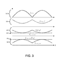
- FIG. 3 illustrates example signals that may be exhibited by a boost rectifier during operation.
- the first waveform 310 shows an example variation of choke current that may be exhibited during operation of the boost converter over one cycle of the AC voltage input to the rectifier.
- the second waveform 320 shows variation in inductance exhibited by the inductor as a result of the choke current shown in waveform 310.
- Waveform 360 shows an example crossover frequency resulting from the variation in inductance shown in waveform 320 when a constant gain (K p_constant ), as shown in waveform 340, is used to adjust a feedback signal.
- K p_constant may be calculated to be constant based on minimum inductance at maximum current. Therefore, the crossover frequency, where ac voltage is zero-crossing or lower input current conditions, is reduced when larger inductance. Such reduction in the crossover frequency may lead to current distortion due to limited bandwidth.
- Waveform 350 shows an example crossover frequency resulting from the variation in inductance shown in waveform 320 when a gain K p (I ref ) is dynamically adjusted based on the inductance of the inductor as shown in waveform 330.
- dynamic adjustment of the gain as a function of the inductance can be used to achieve a crossover frequency that is substantially constant across varying operating conditions.
- a digital control loop may be used to update a feedback signal and/or gain thereof.
- an apparatus may include a digitally controlled 750W power-factor compensated power converter.
- the converter has 627uH L initial and 219uH at 0A and 12.5A bias current, and K choke is 32.6uH/A.
- the measured input power factor and THD at adaptive gain is compared with constant gain as shown in Table 1. Power factor can be increased 0.01 averagely at different loading conditions while THD can be decreased as well.
- a digital control loop is configured to update a feedback signal using variable gain based on inductance.
- the digital control loop can be implemented with low speed MCU, thereby lowering manufacturing costs and power consumption.
- Some other embodiments may implement a control loop using dedicated hardware peripherals to shorten the phase delay.
- a "block” (also sometimes “logic circuitry” or “module”) is a circuit that carries out one or more of these or related operations/activities (e.g., high-speed sampling buffer, or filter).
- one or more modules are discrete logic circuits or programmable logic circuits configured and arranged for implementing these operations/activities, as in the circuit modules shown in FIGs. 1 and 2 .
- such a programmable circuit is one or more computer circuits programmed to execute a set (or sets) of instructions (and/or configuration data).
- the instructions can be in the form of firmware or software stored in and accessible from a memory (circuit).
- first and second modules include a combination of a CPU hardware-based circuit and a set of instructions in the form of firmware, where the first module includes a first CPU hardware circuit with one set of instructions and the second module includes a second CPU hardware circuit with another set of instructions.
- Certain embodiments are directed to a computer program product (e.g., nonvolatile memory device), which includes a machine or computer-readable medium having stored thereon instructions which may be executed by a computer (or other electronic device) to perform these operations/activities.
- a computer program product e.g., nonvolatile memory device
Landscapes
- Engineering & Computer Science (AREA)
- Power Engineering (AREA)
- Dc-Dc Converters (AREA)
Abstract
Description
- Aspects of various embodiments of the present disclosure are related to power factor correction in power converters.
- A boost converter is a type of switching power supply capable of providing a regulated output voltage that is higher than a rectified input voltage. An example boost converter includes an inductor, an output capacitor, and a switching circuit. The switching circuit adjusts current paths in the boost converter to alternately charge and discharge the inductor and an output capacitor. In a first mode, the switching circuit adjusts current paths to charge an inductor. In a second mode, the switching circuit adjusts current paths to transfer charge from the inductor to the output capacitor. Voltage across the output capacitor is provided as an output voltage of the boost converter.
- The inductance exhibited by the inductor of a boost converter depends on a biasing current through the inductor. For example, inductance exhibited by an inductor may decrease as current through the inductor is increased. For ease of reference, the current through the inductor may be referred to as a choke current. The relationship between the inductance and the choke current is particularly apparent when the core of an inductor is composed of magnetic powder. Inductors having magnetic powder cores are widely used power converters because they exhibit soft saturation, low cost, and high power density.
- Due to the relationship between the inductance and the choke current, inductance exhibited by the inductor may vary under different operating conditions (e.g., different load conditions). Such variation of inductance can make it difficult to adjust switching control of a power converter for optimal efficiency. For example, some boost converters use a feedback loop having a constant gain to control switching circuitry that switches the boost converter between the first and second modes of operation. The gain of the feedback loop may be set, for example, based on a minimum inductance corresponding to a maximum choke current at a minimum input voltage and full output power. However, if operating conditions cause choke current to decrease, the inductance exhibited by the inductor is increased-thereby decreasing cross-over frequency of the boost converter and resulting in a poor power factor and poor total harmonic distortion (THD).
- Various example embodiments are directed to methods, circuits, and apparatuses for power conversion.
- Methods are disclosed for power conversion. In an example embodiment, a boost converter is provided. The boost converter includes a current loop that is affected by at least one compensation correction parameter and by variation in an inductance of the current loop. Using a power factor correction circuit, the compensation correction parameter is adaptively modified based on variation in the inductance of the current loop.
- Circuits and apparatuses for power conversion are also disclosed. In an example embodiment, an apparatus includes a boost converter having a current loop affected by at least one compensation correction parameter and variation in an inductance of the current loop. The apparatus also includes a power factor correction means, including a circuit, configured and arranged to adaptively modify the compensation correction parameter based on variation in the inductance of the current loop.
- The above discussion/summary is not intended to describe each embodiment or every implementation of the present disclosure. The figures and detailed description that follow also exemplify various embodiments.
- Various example embodiments may be more completely understood in consideration of the following detailed description in connection with the accompanying drawings, in which:
-
FIG. 1 shows a block diagram of a first power converter circuit, configured in accordance with one or more embodiments; -
FIG. 2 shows a block diagram of a second power converter circuit, configured in accordance with one or more embodiments; and -
FIG. 3 illustrates example signals that may be exhibited by a boost rectifier during operation. - While various embodiments discussed herein are amenable to modifications and alternative forms, aspects thereof have been shown by way of example in the drawings and will be described in detail. It should be understood, however, that the intention is not to limit the invention to the particular embodiments described. On the contrary, the intention is to cover all modifications, equivalents, and alternatives falling within the scope of the disclosure, including aspects defined in the claims. In addition, the term "example" as used throughout this application is only by way of illustration, and not limitation.
- Aspects of the present disclosure are believed to be applicable to a variety of different types of apparatuses, systems and methods involving power conversion. While not necessarily so limited, various aspects may be appreciated through a discussion of examples using this context.
- Various example embodiments are directed to methods, circuits and apparatuses for power conversion are disclosed. In an example embodiment, an apparatus includes a boost converter having a current loop affected by at least one compensation correction parameter and variation in an inductance of the current loop. The apparatus also includes a power factor correction means, including a circuit, configured and arranged to adaptively modify the compensation correction parameter based on variation in the inductance of the current loop. The power factor correction means dynamically adjusts the compensation correction parameter, based on the inductance, to mitigate reduction of the power factor of the boost converter due to the variation in the inductance.
- In some embodiments, the boost converter includes an inductor in the current loop and a switching circuit. The switching circuit increases current through the inductor when closed, thereby charging the inductor. When the switching circuit is opened, charge is transferred from the inductor to an output capacitor. In some implementations, the switching circuit is configured and arranged to close in response to pulses in a control signal and open when pulses are not present in the control signal. Width of pulses may be adjusted by a pulse width modulator based on a feedback signal to ensure that a desired voltage and/or current is output by the boost converter. The feedback signal may be generated, for example, based on a difference between a measured current through the inductor and a reference current derived from a product of a voltage output by the boost converter multiplied by an input reference voltage.
- The power factor correction circuit is configured and arranged to adjust a gain of the feedback signal based on variation in the inductance of the inductor. In some implementations, the power factor correction circuit adjusts the gain of the feedback to exhibit a variation that is substantially equal to a variation in the inductance of the inductor. In some implementations, a power factor correction circuit may adjust the gain based on the reference current used to generate the feedback signal. As the choke current is forced to follow the reference current typical, the reference current exhibits a variation that is proportional to the variation of current through the inductor and may be used to determine variation of inductance of the inductor.
- Turning now to the figures,
FIG. 1 shows a block diagram of a first power converter circuit configured in accordance with one or more embodiments. Thepower converter circuit 100 includes arectifier 110 configured to rectify an AC voltage to produce a DC voltage. Aboost converter 120 is connected to receive the DC voltage from therectifier 110. Theboost converter 120 includes aninductor 122, adiode 124, anoutput capacitor 126, and aswitching circuit 128. Theswitching circuit 128 adjusts current loops in theboost converter 120 to alternately charge and discharge theinductor 122 andoutput capacitor 126. In a first mode and a second mode, DC current passes from therectifier 110 through theinductor 122 anddiode 124, to theoutput capacitor 126. In the first mode, theswitching circuit 128 is closed to provide an additional current path from theinductor 122 to ground. The current path through theswitching circuit 128 increases the current through theinductor 122, thereby charging the inductor. While in the first mode, thediode 124 prevents the current path through theswitching circuit 128 from discharging theoutput capacitor 126. In the second mode, theswitching circuit 128 is opened and charge stored in theinductor 122 is transferred to theoutput capacitor 126 via thediode 124. Voltage across theoutput capacitor 126 is provided as an output voltage to aresistive load 130. - The opening and closing of the
switching circuit 128 is controlled by a feedback loop. In this example, theswitching circuit 128 is configured to close in response to pulses in a control signal (Ctrl) output by apulse width modulator 140. The pulse width modulator adjusts duration of the pulses in response to a feedback signal. The feedback signal is generated by afeedback circuit 160 to ensure that a desired voltage and/or current is output by the boost converter. The feedback signal may be generated, for example, based on a difference between a measured current through theinductor 122 and a reference current. The reference current may be derived, for example from a product of a voltage output by theboost converter 120 multiplied by an input reference voltage. - The
power converter circuit 100, includes acompensation circuit 150 configured to adaptively adjust the feedback signal generated by thefeedback circuit 160 to compensate for variation in the inductance of the current loop. In some implementations, thecompensation circuit 150 is configured to adjust a gain of the feedback signal generated by thefeedback circuit 160 based on the inductance exhibited by theinductor 122. Thecompensation circuit 150 provides the resulting feedback signal to thepulse width modulator 140. -
FIG. 2 shows a block diagram of a power converter circuit configured in accordance with one or more embodiments. Thepower converter circuit 200 includes arectifier 210 configured to rectify an AC voltage to produce a DC voltage. Aboost converter 220 is connected to receive the DC voltage from therectifier 210. Theboost converter 220 includes aninductor 222, adiode 224, anoutput capacitor 226, and aswitching circuit 228. Arranged as described with reference toinductor 122,diode 124,output capacitor 126, and switchingcircuit 128 of theboost converter 120 shown inFIG. 1 . The voltage across theoutput capacitor 226 is output to aresistive load 230. - The opening and closing of the
switching circuit 228 is controlled by pulses in a control signal (Ctrl) output by apulse width modulator 240. Thepulse width modulator 240 adjusts duration of the pulses in response to a feedback signal. The feedback signal is generated by afeedback circuit 260 to ensure that a desired voltage and/or current is output by theboost converter 220. In this example, the feedback signal is generated by thefeedback circuit 260 based on a difference between a measured current through the inductor 222 (Isen) and a reference current (Iref). The reference current Iref may be generated based on peak detection of an input voltage, a voltage (Vsen) output by theboost converter 220, an input reference voltage (Vref), and the choke current through theinductor 222. In some implementations, various ones of the measured voltages and/or currents may be respectfully scaled by respective scaling circuits (e.g., 272, 274, 276, and 278). For additional information regarding amount of scaling of these voltages and/or currents, reference may be made to High Power Factor Preregulator for Off-Line Power Supplies, Lloyd, H. Dixon Jr. (Unitrode (now Texas Inst.) Power Supply Design Seminar, SEM-800, 1991), which is fully incorporated by reference herein. - The reference current for one example implementation may be expressed as:

where Gvea_out is given by
and where typical proportional-integral compensation Gvea(s) is given by
- The
power converter circuit 200, includes acompensation circuit 250 configured to adaptively adjust the feedback signal generated by thefeedback circuit 260 to compensate for variation in the inductance of the current loop. In some implementations, thecompensation circuit 250 is configured to adjust a gain of the feedback signal generated by thefeedback circuit 260, based on the inductance exhibited by theinductor 222. The transfer function of proportional-integral compensation performed by thecompensation circuit 250 is expressed by:
- Where, Kp (Iref) is a dynamic gain adjustment performed by the
compensation circuit 250. An example dynamic gain adjustment that may be performed is expressed as:
- The open loop transfer function of the boost converter may be expressed as:

- As long as Kp(Iref) keeps same variation as L(Iref), the impact of inductance variation to the transfer function can be eliminated and the cross-over frequency can be maximized.
- Since the inductance can be approximated to be linear to its biasing current,

- Linitial is the maximum inductance at zero biasing current and Kchoke is the approximated linear gain. Accordingly, the open loop transfer function is rewritten as

- Kpmax is determined by the Linitial and loop stability. Kref is calculated to eliminate the variation of Iref.

- The compensation gain Kp changes adaptively to Iref and the crossover frequency is maximized for different conditions.
-
FIG. 3 illustrates example signals that may be exhibited by a boost rectifier during operation. Thefirst waveform 310 shows an example variation of choke current that may be exhibited during operation of the boost converter over one cycle of the AC voltage input to the rectifier. Thesecond waveform 320 shows variation in inductance exhibited by the inductor as a result of the choke current shown inwaveform 310. -
Waveform 360 shows an example crossover frequency resulting from the variation in inductance shown inwaveform 320 when a constant gain (Kp_constant), as shown inwaveform 340, is used to adjust a feedback signal. As previously indicated, the feedback loop gain Kp_constant may be calculated to be constant based on minimum inductance at maximum current. Therefore, the crossover frequency, where ac voltage is zero-crossing or lower input current conditions, is reduced when larger inductance. Such reduction in the crossover frequency may lead to current distortion due to limited bandwidth. -
Waveform 350 shows an example crossover frequency resulting from the variation in inductance shown inwaveform 320 when a gain Kp (Iref) is dynamically adjusted based on the inductance of the inductor as shown inwaveform 330. As shown inwaveform 350, dynamic adjustment of the gain as a function of the inductance can be used to achieve a crossover frequency that is substantially constant across varying operating conditions. - The blocks, modules, circuits and functions shown or discussed with reference to the examples may be implemented using various analog or digital circuits. For example, in some embodiments, a digital control loop may be used to update a feedback signal and/or gain thereof. In some embodiments, an apparatus may include a digitally controlled 750W power-factor compensated power converter. In one implementation, the converter has 627uH Linitial and 219uH at 0A and 12.5A bias current, and K choke is 32.6uH/A. The measured input power factor and THD at adaptive gain is compared with constant gain as shown in Table 1. Power factor can be increased 0.01 averagely at different loading conditions while THD can be decreased as well. By this improvement, more power factor margin of power supply is achieved to pass the international standard, such as PF>0.95 at 50% load by 80plus Platinum for server power supply.
Table 1 Pout (W) @230Vac Adaptive gain Constant gain PF iTHD PF iTHD 75 0.709 66.68 0.686 73.68 150 0.861 40.36 0.848 44.62 375 0.972 7.05 0.959 12.46 560 0.985 5.37 0.979 8.93 750 0.991 4.76 0.987 7.13 - Some solutions to improve power factor and THD increase the updating frequency of a control loop, so as to reduce the phase delay of digital loop for higher crossover frequency. However, the calculation speed of a control loop is determined directly by microcontroller (MCU) clock speed, which means that higher MCU clock speed has to be used at a higher cost and power consumption. In some embodiments, a digital control loop is configured to update a feedback signal using variable gain based on inductance. The digital control loop can be implemented with low speed MCU, thereby lowering manufacturing costs and power consumption. Some other embodiments may implement a control loop using dedicated hardware peripherals to shorten the phase delay.
- Various blocks, modules or other circuits may be implemented to carry out one or more of the operations and activities described herein and/or shown in the figures. In these contexts, a "block" (also sometimes "logic circuitry" or "module") is a circuit that carries out one or more of these or related operations/activities (e.g., high-speed sampling buffer, or filter). For example, in certain of the above-discussed embodiments, one or more modules are discrete logic circuits or programmable logic circuits configured and arranged for implementing these operations/activities, as in the circuit modules shown in
FIGs. 1 and2 . In certain embodiments, such a programmable circuit is one or more computer circuits programmed to execute a set (or sets) of instructions (and/or configuration data). The instructions (and/or configuration data) can be in the form of firmware or software stored in and accessible from a memory (circuit). As an example, first and second modules include a combination of a CPU hardware-based circuit and a set of instructions in the form of firmware, where the first module includes a first CPU hardware circuit with one set of instructions and the second module includes a second CPU hardware circuit with another set of instructions. - Certain embodiments are directed to a computer program product (e.g., nonvolatile memory device), which includes a machine or computer-readable medium having stored thereon instructions which may be executed by a computer (or other electronic device) to perform these operations/activities.
- Based upon the above discussion and illustrations, those skilled in the art will readily recognize that various modifications and changes may be made to the various embodiments without strictly following the exemplary embodiments and applications illustrated and described herein. For example, although aspects and features may in some cases be described in individual figures, it will be appreciated that features from one figure can be combined with features of another figure even though the combination is not explicitly shown or explicitly described as a combination. Further, various aspects of individual embodiments may be implemented as separate embodiments. Such modifications do not depart from the true spirit and scope of various aspects of the invention, including aspects set forth in the claims.
Claims (9)
- A method comprising:providing a boost converter having a current loop affected by at least one compensation correction parameter and variation in an inductance of the current loop; andusing a power factor correction circuit, adaptively modifying the compensation correction parameter based on variation in the inductance of the current loop.
- The method of claim 1, wherein:the boost converter includes an inductor in the current loop and includes a switching circuit configured and arranged to increase current through the inductor, and thereby charge the inductor, when closed;the switching circuit is configured and arranged to close in response to pulses of a control signal; andfurther comprising adjusting a pulse width of the pulses of the control signal based on a feedback signal and, using the power factor correction circuit, adjusting a gain of the feedback signal based on variation in the inductance of the inductor.
- The method of claim 2, wherein the adjusting of the gain of the feedback signal by the power factor correction circuit adjusts the gain to exhibit a variation in the gain that is substantially equal to a variation in the inductance of the inductor.
- The method of claim 2 or 3, further comprising generating the feedback signal based on a difference between a measured current through the inductor and a reference current derived from a product of a voltage output by the boost converter multiplied with an input reference voltage.
- The method of claim 4, wherein the adjusting of the gain of the feedback signal dynamically adjusts the gain as a function of the reference current.
- The method of any preceding claim, wherein the boost converter exhibits a power factor that is reduced by variation in the inductance; and
the adaptive modifying of the compensation correction parameter based on variation in the inductance mitigates reduction of the power factor due to the variation in the inductance. - An apparatus, including
a boost converter having a current loop affected by at least one compensation correction parameter and variation in an inductance of the current loop; and
a power factor correction means, including a circuit, configured and arranged to adaptively modify the compensation correction parameter based on variation in the inductance of the current loop. - The apparatus of claim 7, further comprising:a pulse width modulator configured modulate a width of pulses in a control signal based on a feedback signal, wherein
the boost converter includes an inductor in the current loop and a switching circuit configured and arranged to increase current through the inductor, and thereby charge the inductor, when closed;
the switching circuit is configured and arranged to close in response to the pulses of the control signal; and
the power factor correction means is configured and arranged to adjust a gain of the feedback signal based on variation in the inductance of the inductor. - The apparatus of claim 8, wherein the power factor correction means is configured and arranged to cause a variation in the gain of the feedback signal to be substantially equal to the variation in the inductance of the inductor.
Applications Claiming Priority (1)
| Application Number | Priority Date | Filing Date | Title |
|---|---|---|---|
| US14/473,146 US9431894B2 (en) | 2014-08-29 | 2014-08-29 | Inductance variation based compensation in boost converter |
Publications (2)
| Publication Number | Publication Date |
|---|---|
| EP2991211A1 true EP2991211A1 (en) | 2016-03-02 |
| EP2991211B1 EP2991211B1 (en) | 2018-11-14 |
Family
ID=53776494
Family Applications (1)
| Application Number | Title | Priority Date | Filing Date |
|---|---|---|---|
| EP15179854.3A Active EP2991211B1 (en) | 2014-08-29 | 2015-08-05 | Power factor correction in power converter |
Country Status (3)
| Country | Link |
|---|---|
| US (1) | US9431894B2 (en) |
| EP (1) | EP2991211B1 (en) |
| CN (1) | CN105391296B (en) |
Cited By (2)
| Publication number | Priority date | Publication date | Assignee | Title |
|---|---|---|---|---|
| WO2020123654A1 (en) * | 2018-12-13 | 2020-06-18 | Power Integrations, Inc. | Apparatus and methods for controllable networks to vary inter-stage power transfer in a multi-stage power conversion system |
| CN113433839A (en) * | 2021-06-28 | 2021-09-24 | 杭州电子科技大学 | Synchronous rectification Boost converter simulation circuit based on virtual inductor and virtual capacitor |
Families Citing this family (13)
| Publication number | Priority date | Publication date | Assignee | Title |
|---|---|---|---|---|
| US9966841B2 (en) * | 2015-05-18 | 2018-05-08 | Texas Instruments Incorporated | Power factor correction |
| US10146243B2 (en) * | 2016-07-08 | 2018-12-04 | Hyundai Motor Company | Method and system of controlling power factor correction circuit |
| IT201700031159A1 (en) * | 2017-03-21 | 2018-09-21 | St Microelectronics Srl | CONTROL UNIT OF A CONVERTER IN SWITCHING OPERATING IN CONTINUOUS CONDUCTION MODE AND IN PEAK CURRENT CONTROL |
| CN106685210B (en) * | 2017-03-22 | 2019-03-05 | 矽力杰半导体技术(杭州)有限公司 | Power factor correction circuit, control method and controller |
| IT201700073773A1 (en) * | 2017-07-05 | 2019-01-05 | St Microelectronics Srl | CONTROL MODULE FOR A CONSTANT SWITCH-ON CONVERTER AND METHOD OF CHECKING A SWITCHING CONVERTER |
| JP7283094B2 (en) * | 2019-02-04 | 2023-05-30 | 富士電機株式会社 | Drive signal generation circuit, power factor correction circuit |
| CN110086336B (en) | 2019-05-31 | 2021-08-24 | 矽力杰半导体技术(杭州)有限公司 | Power factor correction circuit, control method and controller |
| CN110212741B (en) | 2019-05-31 | 2020-12-11 | 矽力杰半导体技术(杭州)有限公司 | Power factor correction circuit, control method and controller |
| US12081127B2 (en) * | 2019-08-21 | 2024-09-03 | Mitsubishi Electric Corporation | Power conversion device |
| US11711009B2 (en) * | 2019-10-24 | 2023-07-25 | The Trustees Of Columbia University In The City Of New York | Methods, systems, and devices for soft switching of power converters |
| JPWO2021106712A1 (en) * | 2019-11-26 | 2021-06-03 | ||
| CN113078810B (en) * | 2021-04-30 | 2022-06-24 | 深圳市龙星辰电源有限公司 | Intelligent power factor correction method for medical switching power supply |
| CN115549463A (en) * | 2022-10-24 | 2022-12-30 | 广东泰坦智能动力有限公司 | A single-phase power factor correction control method based on multiplier voltage regulation input impedance |
Citations (1)
| Publication number | Priority date | Publication date | Assignee | Title |
|---|---|---|---|---|
| US20120087159A1 (en) * | 2010-10-11 | 2012-04-12 | Solarbridge Technologies, Inc. | Quadrature-corrected feedforward control apparatus and method for dc-ac power conversion |
Family Cites Families (9)
| Publication number | Priority date | Publication date | Assignee | Title |
|---|---|---|---|---|
| US4761725A (en) * | 1986-08-01 | 1988-08-02 | Unisys Corporation | Digitally controlled A.C. to D.C. power conditioner |
| US4683529A (en) * | 1986-11-12 | 1987-07-28 | Zytec Corporation | Switching power supply with automatic power factor correction |
| US4885675A (en) | 1988-10-07 | 1989-12-05 | Unisys Corporation | Transformer isolated AC to DC power conditioner with resistive input current |
| US7042207B1 (en) * | 2003-11-07 | 2006-05-09 | National Semiconductor Corporation | Inductive measurement system and method |
| US8461816B2 (en) * | 2010-02-25 | 2013-06-11 | International Rectifier Corporation | Coefficient scaling depending on number of active phases |
| JP5902401B2 (en) * | 2011-05-31 | 2016-04-13 | サイプレス セミコンダクター コーポレーション | Power supply device, control circuit, electronic device, and power supply control method |
| US8937469B2 (en) * | 2012-10-09 | 2015-01-20 | Delta-Q Technologies Corp. | Digital controller based detection methods for adaptive mixed conduction mode power factor correction circuit |
| US9912238B1 (en) * | 2013-07-26 | 2018-03-06 | Cirrus Logic, Inc. | Determination of inductor current during reverse current in a boost converter |
| CN103997040B (en) * | 2014-05-09 | 2016-10-19 | 安徽振兴科技股份有限公司 | Improve active electric filter device harmonic wave control and the method for reactive-load compensation effect |
-
2014
- 2014-08-29 US US14/473,146 patent/US9431894B2/en active Active
-
2015
- 2015-08-05 EP EP15179854.3A patent/EP2991211B1/en active Active
- 2015-08-27 CN CN201510535507.1A patent/CN105391296B/en active Active
Patent Citations (1)
| Publication number | Priority date | Publication date | Assignee | Title |
|---|---|---|---|---|
| US20120087159A1 (en) * | 2010-10-11 | 2012-04-12 | Solarbridge Technologies, Inc. | Quadrature-corrected feedforward control apparatus and method for dc-ac power conversion |
Non-Patent Citations (4)
| Title |
|---|
| LLOYD, H. DIXON JR: "High Power Factor Preregulator for OffLine Power Supplies", POWER SUPPLY DESIGN SEMINAR, 1991 |
| LLOYD, H. DIXON JR: "High Power Factor Preregulator for OffLine Power Supplies", POWER SUPPLY DESIGN SEMINAR, 1991, XP002747990 * |
| WANG C-M: "A Novel ZCS-PWM Power-Factor Preregulator With Reduced Conduction Losses", IEEE TRANSACTIONS ON INDUSTRIAL ELECTRONICS, IEEE SERVICE CENTER, PISCATAWAY, NJ, USA, vol. 52, no. 3, 1 June 2005 (2005-06-01), pages 689 - 700, XP011133047, ISSN: 0278-0046, DOI: 10.1109/TIE.2005.843967 * |
| YU QIN ET AL: "Fuzzy logic and digital PI control of single phase power factor preregulator for an online UPS-a comparative study", INDUSTRIAL TECHNOLOGY, 1996. (ICIT '96)., PROCEEDINGS OF THE IEEE INTE RNATIONAL CONFERENCE ON SHANGHAI, CHINA 2-6 DEC. 1996, NEW YORK, NY, USA,IEEE, US, 2 December 1996 (1996-12-02), pages 103 - 107, XP010232594, ISBN: 978-0-7803-3104-4 * |
Cited By (5)
| Publication number | Priority date | Publication date | Assignee | Title |
|---|---|---|---|---|
| WO2020123654A1 (en) * | 2018-12-13 | 2020-06-18 | Power Integrations, Inc. | Apparatus and methods for controllable networks to vary inter-stage power transfer in a multi-stage power conversion system |
| CN113169677A (en) * | 2018-12-13 | 2021-07-23 | 电力集成公司 | Apparatus and method for a controllable network to vary inter-stage power transfer in a multi-stage power conversion system |
| US12119743B2 (en) | 2018-12-13 | 2024-10-15 | Power Integrations, Inc. | Apparatus and methods for controllable networks to vary inter-stage power transfer in a multi-stage power conversion system |
| CN113433839A (en) * | 2021-06-28 | 2021-09-24 | 杭州电子科技大学 | Synchronous rectification Boost converter simulation circuit based on virtual inductor and virtual capacitor |
| CN113433839B (en) * | 2021-06-28 | 2022-07-01 | 杭州电子科技大学 | Synchronous rectification Boost converter simulation circuit based on virtual inductor and virtual capacitor |
Also Published As
| Publication number | Publication date |
|---|---|
| CN105391296A (en) | 2016-03-09 |
| EP2991211B1 (en) | 2018-11-14 |
| US20160065054A1 (en) | 2016-03-03 |
| CN105391296B (en) | 2018-09-21 |
| US9431894B2 (en) | 2016-08-30 |
Similar Documents
| Publication | Publication Date | Title |
|---|---|---|
| US9431894B2 (en) | Inductance variation based compensation in boost converter | |
| US10411613B2 (en) | Inductive power transfer control | |
| US10218256B2 (en) | Primary side control of primary resonant flyback converters | |
| EP2775599B1 (en) | Boost converter | |
| US9866114B2 (en) | Transitioning a power supply from a mode to another mode in response to a length of a portion of a current pulse | |
| CN101887282B (en) | Closed loop negative feedback system with low frequency modulated gain | |
| US7123494B2 (en) | Power factor correction circuit and method of varying switching frequency | |
| US20110292699A1 (en) | Systems and Methods for Distortion Reduction | |
| KR102158074B1 (en) | Open-loop charge pump | |
| TW201722045A (en) | Power factor correction conversion apparatus and control method thereof comprising a rectification step, a feedback step, a ripple calculation step, a ripple offset step, a logic operation step, a pulse-width modulation step, and a power factor correction step | |
| US10873215B2 (en) | Resonant regulating rectifier with an integrated antenna | |
| US20070236201A1 (en) | Correction circuit for improved load transient response | |
| US9899935B2 (en) | Power factor correction device with first and second output parts | |
| US10284078B1 (en) | Apparatus and method for limiting electromagnetic interferences in a switching converter | |
| US8675375B2 (en) | System and method for input voltage transient response control | |
| US11431262B2 (en) | Power conversion method and system | |
| US7315150B1 (en) | Method of power conversion and apparatus which achieves high power factor correction using ripple current mode control | |
| US20160233772A1 (en) | Power regulator and slope compensation | |
| Narasimharaju | Enhanced closed loop voltage control of buck converter for improved performance | |
| US20180337604A1 (en) | Dc-dc conversion circuit system and forming method thereof | |
| US20260031712A1 (en) | Switching power converters, and methods and control modules for operating same | |
| US20060285373A1 (en) | Power factor correction circuit | |
| Thottuvelil et al. | Improving THD in single-phase high-power-factor rectifiers | |
| HK1081334A1 (en) | Power factor correction circuit and method of varying switching frequency | |
| HK1081334B (en) | Power factor correction circuit and method of varying switching frequency |
Legal Events
| Date | Code | Title | Description |
|---|---|---|---|
| PUAI | Public reference made under article 153(3) epc to a published international application that has entered the european phase |
Free format text: ORIGINAL CODE: 0009012 |
|
| AK | Designated contracting states |
Kind code of ref document: A1 Designated state(s): AL AT BE BG CH CY CZ DE DK EE ES FI FR GB GR HR HU IE IS IT LI LT LU LV MC MK MT NL NO PL PT RO RS SE SI SK SM TR |
|
| AX | Request for extension of the european patent |
Extension state: BA ME |
|
| 17P | Request for examination filed |
Effective date: 20160902 |
|
| RBV | Designated contracting states (corrected) |
Designated state(s): AL AT BE BG CH CY CZ DE DK EE ES FI FR GB GR HR HU IE IS IT LI LT LU LV MC MK MT NL NO PL PT RO RS SE SI SK SM TR |
|
| GRAP | Despatch of communication of intention to grant a patent |
Free format text: ORIGINAL CODE: EPIDOSNIGR1 |
|
| STAA | Information on the status of an ep patent application or granted ep patent |
Free format text: STATUS: GRANT OF PATENT IS INTENDED |
|
| INTG | Intention to grant announced |
Effective date: 20180705 |
|
| RIN1 | Information on inventor provided before grant (corrected) |
Inventor name: CHEONG, CHAN YOKE Inventor name: LI, DONG |
|
| GRAJ | Information related to disapproval of communication of intention to grant by the applicant or resumption of examination proceedings by the epo deleted |
Free format text: ORIGINAL CODE: EPIDOSDIGR1 |
|
| STAA | Information on the status of an ep patent application or granted ep patent |
Free format text: STATUS: REQUEST FOR EXAMINATION WAS MADE |
|
| GRAP | Despatch of communication of intention to grant a patent |
Free format text: ORIGINAL CODE: EPIDOSNIGR1 |
|
| STAA | Information on the status of an ep patent application or granted ep patent |
Free format text: STATUS: GRANT OF PATENT IS INTENDED |
|
| GRAS | Grant fee paid |
Free format text: ORIGINAL CODE: EPIDOSNIGR3 |
|
| INTC | Intention to grant announced (deleted) | ||
| GRAA | (expected) grant |
Free format text: ORIGINAL CODE: 0009210 |
|
| STAA | Information on the status of an ep patent application or granted ep patent |
Free format text: STATUS: THE PATENT HAS BEEN GRANTED |
|
| INTG | Intention to grant announced |
Effective date: 20180926 |
|
| AK | Designated contracting states |
Kind code of ref document: B1 Designated state(s): AL AT BE BG CH CY CZ DE DK EE ES FI FR GB GR HR HU IE IS IT LI LT LU LV MC MK MT NL NO PL PT RO RS SE SI SK SM TR |
|
| REG | Reference to a national code |
Ref country code: CH Ref legal event code: EP Ref country code: AT Ref legal event code: REF Ref document number: 1066009 Country of ref document: AT Kind code of ref document: T Effective date: 20181115 |
|
| REG | Reference to a national code |
Ref country code: DE Ref legal event code: R096 Ref document number: 602015019731 Country of ref document: DE |
|
| REG | Reference to a national code |
Ref country code: IE Ref legal event code: FG4D |
|
| REG | Reference to a national code |
Ref country code: NL Ref legal event code: MP Effective date: 20181114 |
|
| REG | Reference to a national code |
Ref country code: LT Ref legal event code: MG4D |
|
| REG | Reference to a national code |
Ref country code: AT Ref legal event code: MK05 Ref document number: 1066009 Country of ref document: AT Kind code of ref document: T Effective date: 20181114 |
|
| PG25 | Lapsed in a contracting state [announced via postgrant information from national office to epo] |
Ref country code: FI Free format text: LAPSE BECAUSE OF FAILURE TO SUBMIT A TRANSLATION OF THE DESCRIPTION OR TO PAY THE FEE WITHIN THE PRESCRIBED TIME-LIMIT Effective date: 20181114 Ref country code: BG Free format text: LAPSE BECAUSE OF FAILURE TO SUBMIT A TRANSLATION OF THE DESCRIPTION OR TO PAY THE FEE WITHIN THE PRESCRIBED TIME-LIMIT Effective date: 20190214 Ref country code: LT Free format text: LAPSE BECAUSE OF FAILURE TO SUBMIT A TRANSLATION OF THE DESCRIPTION OR TO PAY THE FEE WITHIN THE PRESCRIBED TIME-LIMIT Effective date: 20181114 Ref country code: IS Free format text: LAPSE BECAUSE OF FAILURE TO SUBMIT A TRANSLATION OF THE DESCRIPTION OR TO PAY THE FEE WITHIN THE PRESCRIBED TIME-LIMIT Effective date: 20190314 Ref country code: NO Free format text: LAPSE BECAUSE OF FAILURE TO SUBMIT A TRANSLATION OF THE DESCRIPTION OR TO PAY THE FEE WITHIN THE PRESCRIBED TIME-LIMIT Effective date: 20190214 Ref country code: LV Free format text: LAPSE BECAUSE OF FAILURE TO SUBMIT A TRANSLATION OF THE DESCRIPTION OR TO PAY THE FEE WITHIN THE PRESCRIBED TIME-LIMIT Effective date: 20181114 Ref country code: AT Free format text: LAPSE BECAUSE OF FAILURE TO SUBMIT A TRANSLATION OF THE DESCRIPTION OR TO PAY THE FEE WITHIN THE PRESCRIBED TIME-LIMIT Effective date: 20181114 Ref country code: ES Free format text: LAPSE BECAUSE OF FAILURE TO SUBMIT A TRANSLATION OF THE DESCRIPTION OR TO PAY THE FEE WITHIN THE PRESCRIBED TIME-LIMIT Effective date: 20181114 Ref country code: HR Free format text: LAPSE BECAUSE OF FAILURE TO SUBMIT A TRANSLATION OF THE DESCRIPTION OR TO PAY THE FEE WITHIN THE PRESCRIBED TIME-LIMIT Effective date: 20181114 |
|
| PG25 | Lapsed in a contracting state [announced via postgrant information from national office to epo] |
Ref country code: PT Free format text: LAPSE BECAUSE OF FAILURE TO SUBMIT A TRANSLATION OF THE DESCRIPTION OR TO PAY THE FEE WITHIN THE PRESCRIBED TIME-LIMIT Effective date: 20190314 Ref country code: SE Free format text: LAPSE BECAUSE OF FAILURE TO SUBMIT A TRANSLATION OF THE DESCRIPTION OR TO PAY THE FEE WITHIN THE PRESCRIBED TIME-LIMIT Effective date: 20181114 Ref country code: AL Free format text: LAPSE BECAUSE OF FAILURE TO SUBMIT A TRANSLATION OF THE DESCRIPTION OR TO PAY THE FEE WITHIN THE PRESCRIBED TIME-LIMIT Effective date: 20181114 Ref country code: GR Free format text: LAPSE BECAUSE OF FAILURE TO SUBMIT A TRANSLATION OF THE DESCRIPTION OR TO PAY THE FEE WITHIN THE PRESCRIBED TIME-LIMIT Effective date: 20190215 Ref country code: RS Free format text: LAPSE BECAUSE OF FAILURE TO SUBMIT A TRANSLATION OF THE DESCRIPTION OR TO PAY THE FEE WITHIN THE PRESCRIBED TIME-LIMIT Effective date: 20181114 Ref country code: NL Free format text: LAPSE BECAUSE OF FAILURE TO SUBMIT A TRANSLATION OF THE DESCRIPTION OR TO PAY THE FEE WITHIN THE PRESCRIBED TIME-LIMIT Effective date: 20181114 |
|
| PG25 | Lapsed in a contracting state [announced via postgrant information from national office to epo] |
Ref country code: IT Free format text: LAPSE BECAUSE OF FAILURE TO SUBMIT A TRANSLATION OF THE DESCRIPTION OR TO PAY THE FEE WITHIN THE PRESCRIBED TIME-LIMIT Effective date: 20181114 Ref country code: CZ Free format text: LAPSE BECAUSE OF FAILURE TO SUBMIT A TRANSLATION OF THE DESCRIPTION OR TO PAY THE FEE WITHIN THE PRESCRIBED TIME-LIMIT Effective date: 20181114 Ref country code: PL Free format text: LAPSE BECAUSE OF FAILURE TO SUBMIT A TRANSLATION OF THE DESCRIPTION OR TO PAY THE FEE WITHIN THE PRESCRIBED TIME-LIMIT Effective date: 20181114 Ref country code: DK Free format text: LAPSE BECAUSE OF FAILURE TO SUBMIT A TRANSLATION OF THE DESCRIPTION OR TO PAY THE FEE WITHIN THE PRESCRIBED TIME-LIMIT Effective date: 20181114 |
|
| REG | Reference to a national code |
Ref country code: DE Ref legal event code: R097 Ref document number: 602015019731 Country of ref document: DE |
|
| PG25 | Lapsed in a contracting state [announced via postgrant information from national office to epo] |
Ref country code: SM Free format text: LAPSE BECAUSE OF FAILURE TO SUBMIT A TRANSLATION OF THE DESCRIPTION OR TO PAY THE FEE WITHIN THE PRESCRIBED TIME-LIMIT Effective date: 20181114 Ref country code: EE Free format text: LAPSE BECAUSE OF FAILURE TO SUBMIT A TRANSLATION OF THE DESCRIPTION OR TO PAY THE FEE WITHIN THE PRESCRIBED TIME-LIMIT Effective date: 20181114 Ref country code: RO Free format text: LAPSE BECAUSE OF FAILURE TO SUBMIT A TRANSLATION OF THE DESCRIPTION OR TO PAY THE FEE WITHIN THE PRESCRIBED TIME-LIMIT Effective date: 20181114 Ref country code: SK Free format text: LAPSE BECAUSE OF FAILURE TO SUBMIT A TRANSLATION OF THE DESCRIPTION OR TO PAY THE FEE WITHIN THE PRESCRIBED TIME-LIMIT Effective date: 20181114 |
|
| PLBE | No opposition filed within time limit |
Free format text: ORIGINAL CODE: 0009261 |
|
| STAA | Information on the status of an ep patent application or granted ep patent |
Free format text: STATUS: NO OPPOSITION FILED WITHIN TIME LIMIT |
|
| 26N | No opposition filed |
Effective date: 20190815 |
|
| PG25 | Lapsed in a contracting state [announced via postgrant information from national office to epo] |
Ref country code: SI Free format text: LAPSE BECAUSE OF FAILURE TO SUBMIT A TRANSLATION OF THE DESCRIPTION OR TO PAY THE FEE WITHIN THE PRESCRIBED TIME-LIMIT Effective date: 20181114 |
|
| PG25 | Lapsed in a contracting state [announced via postgrant information from national office to epo] |
Ref country code: TR Free format text: LAPSE BECAUSE OF FAILURE TO SUBMIT A TRANSLATION OF THE DESCRIPTION OR TO PAY THE FEE WITHIN THE PRESCRIBED TIME-LIMIT Effective date: 20181114 |
|
| GBPC | Gb: european patent ceased through non-payment of renewal fee |
Effective date: 20190805 |
|
| PG25 | Lapsed in a contracting state [announced via postgrant information from national office to epo] |
Ref country code: CH Free format text: LAPSE BECAUSE OF NON-PAYMENT OF DUE FEES Effective date: 20190831 Ref country code: MC Free format text: LAPSE BECAUSE OF FAILURE TO SUBMIT A TRANSLATION OF THE DESCRIPTION OR TO PAY THE FEE WITHIN THE PRESCRIBED TIME-LIMIT Effective date: 20181114 Ref country code: LI Free format text: LAPSE BECAUSE OF NON-PAYMENT OF DUE FEES Effective date: 20190831 Ref country code: LU Free format text: LAPSE BECAUSE OF NON-PAYMENT OF DUE FEES Effective date: 20190805 |
|
| REG | Reference to a national code |
Ref country code: BE Ref legal event code: MM Effective date: 20190831 |
|
| PG25 | Lapsed in a contracting state [announced via postgrant information from national office to epo] |
Ref country code: IE Free format text: LAPSE BECAUSE OF NON-PAYMENT OF DUE FEES Effective date: 20190805 |
|
| PG25 | Lapsed in a contracting state [announced via postgrant information from national office to epo] |
Ref country code: GB Free format text: LAPSE BECAUSE OF NON-PAYMENT OF DUE FEES Effective date: 20190805 Ref country code: BE Free format text: LAPSE BECAUSE OF NON-PAYMENT OF DUE FEES Effective date: 20190831 |
|
| PG25 | Lapsed in a contracting state [announced via postgrant information from national office to epo] |
Ref country code: CY Free format text: LAPSE BECAUSE OF FAILURE TO SUBMIT A TRANSLATION OF THE DESCRIPTION OR TO PAY THE FEE WITHIN THE PRESCRIBED TIME-LIMIT Effective date: 20181114 |
|
| PG25 | Lapsed in a contracting state [announced via postgrant information from national office to epo] |
Ref country code: MT Free format text: LAPSE BECAUSE OF FAILURE TO SUBMIT A TRANSLATION OF THE DESCRIPTION OR TO PAY THE FEE WITHIN THE PRESCRIBED TIME-LIMIT Effective date: 20181114 Ref country code: HU Free format text: LAPSE BECAUSE OF FAILURE TO SUBMIT A TRANSLATION OF THE DESCRIPTION OR TO PAY THE FEE WITHIN THE PRESCRIBED TIME-LIMIT; INVALID AB INITIO Effective date: 20150805 |
|
| PG25 | Lapsed in a contracting state [announced via postgrant information from national office to epo] |
Ref country code: MK Free format text: LAPSE BECAUSE OF FAILURE TO SUBMIT A TRANSLATION OF THE DESCRIPTION OR TO PAY THE FEE WITHIN THE PRESCRIBED TIME-LIMIT Effective date: 20181114 |
|
| P01 | Opt-out of the competence of the unified patent court (upc) registered |
Effective date: 20230725 |
|
| PGFP | Annual fee paid to national office [announced via postgrant information from national office to epo] |
Ref country code: DE Payment date: 20250724 Year of fee payment: 11 |
|
| PGFP | Annual fee paid to national office [announced via postgrant information from national office to epo] |
Ref country code: FR Payment date: 20250723 Year of fee payment: 11 |