EP2988421A1 - All-digital phase-locked loop (adpll) with reduced settling time - Google Patents
All-digital phase-locked loop (adpll) with reduced settling time Download PDFInfo
- Publication number
- EP2988421A1 EP2988421A1 EP15178900.5A EP15178900A EP2988421A1 EP 2988421 A1 EP2988421 A1 EP 2988421A1 EP 15178900 A EP15178900 A EP 15178900A EP 2988421 A1 EP2988421 A1 EP 2988421A1
- Authority
- EP
- European Patent Office
- Prior art keywords
- bank
- dco
- frequency
- instructions
- transitory medium
- Prior art date
- Legal status (The legal status is an assumption and is not a legal conclusion. Google has not performed a legal analysis and makes no representation as to the accuracy of the status listed.)
- Withdrawn
Links
- 239000003990 capacitor Substances 0.000 claims description 69
- 238000000034 method Methods 0.000 claims description 12
- 101100129500 Caenorhabditis elegans max-2 gene Proteins 0.000 description 11
- 238000010586 diagram Methods 0.000 description 8
- 238000005259 measurement Methods 0.000 description 5
- 238000010845 search algorithm Methods 0.000 description 5
- 238000004364 calculation method Methods 0.000 description 4
- 230000006870 function Effects 0.000 description 4
- 238000004088 simulation Methods 0.000 description 3
- 238000004422 calculation algorithm Methods 0.000 description 2
- 238000012986 modification Methods 0.000 description 2
- 230000004048 modification Effects 0.000 description 2
- 230000007935 neutral effect Effects 0.000 description 2
- 238000003491 array Methods 0.000 description 1
- 238000004891 communication Methods 0.000 description 1
- 238000012937 correction Methods 0.000 description 1
- 238000013461 design Methods 0.000 description 1
- 230000005669 field effect Effects 0.000 description 1
- 238000012545 processing Methods 0.000 description 1
- 230000035945 sensitivity Effects 0.000 description 1
- 238000012360 testing method Methods 0.000 description 1
Images



Classifications
-
- H—ELECTRICITY
- H03—ELECTRONIC CIRCUITRY
- H03L—AUTOMATIC CONTROL, STARTING, SYNCHRONISATION OR STABILISATION OF GENERATORS OF ELECTRONIC OSCILLATIONS OR PULSES
- H03L7/00—Automatic control of frequency or phase; Synchronisation
- H03L7/06—Automatic control of frequency or phase; Synchronisation using a reference signal applied to a frequency- or phase-locked loop
- H03L7/08—Details of the phase-locked loop
- H03L7/099—Details of the phase-locked loop concerning mainly the controlled oscillator of the loop
- H03L7/0991—Details of the phase-locked loop concerning mainly the controlled oscillator of the loop the oscillator being a digital oscillator, e.g. composed of a fixed oscillator followed by a variable frequency divider
- H03L7/0994—Details of the phase-locked loop concerning mainly the controlled oscillator of the loop the oscillator being a digital oscillator, e.g. composed of a fixed oscillator followed by a variable frequency divider comprising an accumulator
-
- H—ELECTRICITY
- H03—ELECTRONIC CIRCUITRY
- H03L—AUTOMATIC CONTROL, STARTING, SYNCHRONISATION OR STABILISATION OF GENERATORS OF ELECTRONIC OSCILLATIONS OR PULSES
- H03L7/00—Automatic control of frequency or phase; Synchronisation
- H03L7/06—Automatic control of frequency or phase; Synchronisation using a reference signal applied to a frequency- or phase-locked loop
- H03L7/08—Details of the phase-locked loop
- H03L7/099—Details of the phase-locked loop concerning mainly the controlled oscillator of the loop
-
- H—ELECTRICITY
- H03—ELECTRONIC CIRCUITRY
- H03L—AUTOMATIC CONTROL, STARTING, SYNCHRONISATION OR STABILISATION OF GENERATORS OF ELECTRONIC OSCILLATIONS OR PULSES
- H03L7/00—Automatic control of frequency or phase; Synchronisation
- H03L7/06—Automatic control of frequency or phase; Synchronisation using a reference signal applied to a frequency- or phase-locked loop
- H03L7/08—Details of the phase-locked loop
- H03L7/099—Details of the phase-locked loop concerning mainly the controlled oscillator of the loop
- H03L7/0991—Details of the phase-locked loop concerning mainly the controlled oscillator of the loop the oscillator being a digital oscillator, e.g. composed of a fixed oscillator followed by a variable frequency divider
-
- H—ELECTRICITY
- H03—ELECTRONIC CIRCUITRY
- H03L—AUTOMATIC CONTROL, STARTING, SYNCHRONISATION OR STABILISATION OF GENERATORS OF ELECTRONIC OSCILLATIONS OR PULSES
- H03L7/00—Automatic control of frequency or phase; Synchronisation
- H03L7/06—Automatic control of frequency or phase; Synchronisation using a reference signal applied to a frequency- or phase-locked loop
- H03L7/08—Details of the phase-locked loop
- H03L7/10—Details of the phase-locked loop for assuring initial synchronisation or for broadening the capture range
- H03L7/104—Details of the phase-locked loop for assuring initial synchronisation or for broadening the capture range using an additional signal from outside the loop for setting or controlling a parameter in the loop
-
- H—ELECTRICITY
- H03—ELECTRONIC CIRCUITRY
- H03L—AUTOMATIC CONTROL, STARTING, SYNCHRONISATION OR STABILISATION OF GENERATORS OF ELECTRONIC OSCILLATIONS OR PULSES
- H03L2207/00—Indexing scheme relating to automatic control of frequency or phase and to synchronisation
- H03L2207/06—Phase locked loops with a controlled oscillator having at least two frequency control terminals
-
- H—ELECTRICITY
- H03—ELECTRONIC CIRCUITRY
- H03L—AUTOMATIC CONTROL, STARTING, SYNCHRONISATION OR STABILISATION OF GENERATORS OF ELECTRONIC OSCILLATIONS OR PULSES
- H03L2207/00—Indexing scheme relating to automatic control of frequency or phase and to synchronisation
- H03L2207/50—All digital phase-locked loop
Definitions
- Various exemplary embodiments disclosed herein relate generally to all-digital phase-locked loops (ADPLLs) having reduced settling times.
- ADPLLs all-digital phase-locked loops
- ADPLLs may use a time interval to adjust various lock states. During this settling time, disturbances in both phase and frequency may occur. Because of these disturbances, the output signal of the PLL cannot be used during the settling time.
- Various exemplary embodiments relate to a non-transitory medium encoded with instructions for execution of a method of reducing a settling time of a Phase Locked Loop (ADPLL), the non-transitory medium including: instructions for calculating, in a processor, a frequency for a Digital Controlled Oscillator (DCO) by searching for the frequency based upon operational parameters of the DCO; instructions for comparing the calculated frequency to a measured frequency; and instructions for compensating, based upon the comparison, the ADPLL to decrease a settling time.
- DCO Digital Controlled Oscillator
- the DCO may be controlled by a plurality of capacitor banks.
- the plurality of capacitor banks may comprise a Process-Voltage-Temperature (PVT) bank, an Acquisition (ACQ) bank, and a Tracking (TR) bank.
- PVT Process-Voltage-Temperature
- ACQ Acquisition
- TR Tracking
- the instructions for calculating may use either binary or linear searching.
- various exemplary embodiments relate to a hardware device including: a network interface; a memory device; and a processor in communication with the interface memory device, the processor being configured to calculate a frequency for a Digital Controlled Oscillator (DCO) by searching for the frequency based upon operational parameters of the DCO, compare the calculated frequency to a measured frequency, and compensate, based upon the comparison, the ADPLL to decrease a settling time.
- DCO Digital Controlled Oscillator
- the DCO may be configured to be controlled by a plurality of capacitor banks.
- the plurality of capacitor banks may comprise a Process-Voltage-Temperature (PVT) bank, an Acquisition (ACQ) bank, and a Tracking (TR) bank.
- the processor may be configured to set a desired frequency between two smallest possible steps of the TR bank, set a threshold for the TR bank, determine whether the TR bank will exceed the stored threshold, and, when the TR bank is about to exceed the stored threshold, exchange capacitors between banks.
- the processor may also be configured to either exchange capacitors between the TR bank and the ACQ bank, or exchange capacitors between the ACQ bank and the PVT bank.
- the processor may additionally be configured to measure a difference between an ambient temperature and a standard temperature based upon the DCO frequency, store the DCO frequency at the standard temperature, and compare a DCO frequency at the ambient temperature to the stored DCO frequency.
- Fig. 1 illustrates a tuning diagram for an ADPLL.
- the time for locking is on the order of 60 ⁇ s. Because of disturbances in phase and frequency during the settling period before locking, the output signal of the ADPLL cannot be used for reception of a radio signal. For an analog PLL, the output of the receiver would be disturbed too much, while for a digital PLL, loss of data will occur. Thus, locking for ADPLLs may be disrupted.
- DCO digitally controlled oscillator
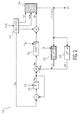
- FIG. 2 illustrates a first embodiment of an improved ADPLL 200.
- ADPLL 200 includes a digitally-controlled oscillator (DCO) model device 210, a ramp generator220, a filter 230, a TDC 240, a divider 250, and a DCO 260. These devices are described in further detail below.
- DCO digitally-controlled oscillator
- the DCO model device 210 receives a Frequency Control Word (FCW) signal as input. Based upon the FCW signal, it produces a Process-Voltage Temperature (PVT) signal and an Acquisition (ACQ) signal. The PVT and ACQ signals are subsequently used for calibration. The DCO model device 210 also forwards a copy of the FCW signal to an adder of ramp generator 220.
- FCW Frequency Control Word
- PVT Process-Voltage Temperature
- ACQ Acquisition
- the ramp generator 220 receives a combination of the FCW signal from the DCO model device 210 and a feedback phase signal as an input signal. Ramp generator 220 then samples this input signal with reference frequency f ref and, in this way, generates a reference phase, ⁇ ref .
- the FCW signal may be added to the content of the register each f ref cycle. In particular, ramp generator 220 may generate the reference phase ⁇ ref by integrating the FCW signal over time.
- each register may represent a number by a certain number of bits.
- Application of the FCW signal results in the content of the register increasing in a staircase shape. This value of the register may continue to increase until a maximum representable number, which is defined by the bit-width of the register, is reached. The register then will "flip over". After flipping over, the content of the register is the modulo value of the sum of the register content and the FCW signal, divided by a maximum number defined by the bit width of the register or any other set maximum number lower than the maximum count defined by the bit width of the register.
- a ramp may be applied to an adder.
- the adder then subtracts the feedback phase from the reference phase.
- the feedback phase is compared to the input phase.
- the difference between the reference and feedback phases is the control signal for the loop.
- a feedback loop then sends the reference phase, ⁇ ref , back to an adder so that it can be combined with the FCW signal to produce the input signal for ramp generator 220.
- Filter 230 receives, from an adder, a combination of the reference phase, ⁇ ref , and a feedback signal, ⁇ v , as an input signal. In the case of linear control, this may be a difference between reference and feedback phases. Other methods might be used to compare the signals. Filter 230 may generate a new TR for the DCO based upon the phase difference during each reference cycle.
- the time-to-digital converter (TDC) 240 receives a DCO output signal (LO) from the DCO 260 as input. This received signal may be a local oscillator (LO) signal. The TDC 240 then compares the phase of the input signal to the phase of the reference frequency f ref to produce output phf f . TDC 240 may provide a resolution enhancement of the phase measurement, e.g., by measuring the position of the reference edge within a DCO period.
- LO local oscillator
- the divider 250 receives the DCO output signal from the DCO 260 and produces phf i as output.
- the combination of phf f and phf i results in ⁇ v .
- the DCO 260 receives the PVT and ACQ signals from the DCO model device 210 as input.
- the DCO 260 receives a TR signal that combines signals from both the DCO model device 210 and the filter 230.
- the DCO 260 may be an inductive-capacitive (LC) oscillator that is controlled by a plurality of capacitor banks.
- the capacitor banks may include a PVT bank, an ACQ bank, and a TR bank. Based upon the PVT, ACQ, and TR signals, DCO 260 produces output, which may be the local oscillator (LO) signal.
- LO local oscillator
- Fig. 3 illustrates an exemplary schematic diagram for a DCO 300.
- the DCO 300 may include a power supply 310, a pair of inductors 320, a PVT capacitor bank 330, an ACQ capacitor bank 340, a TR capacitor bank 350, a pair of transistors 360, an inductor 370, and a ground 380.
- a power supply 310 may be coupled between two inductors 322 and 324 of the pair of inductors 320.
- the opposite ends of inductors 322 and 324 may be coupled to opposing ends of PVT capacitor bank 330, ACQ capacitor bank 340, and TR capacitor bank 350.
- a PVT capacitor bank 330 may include a first capacitor bank 332, a switch 334, and a second capacitor bank 336.
- An input PVT signal may be coupled to switch 334, which may be disposed between first capacitor bank 332 and second capacitor bank 336.
- Each least significant bit (LSB) in the input PVT signal may correspond to a step within a range of 5 MHz to 10 MHz. Each step may be a 5 fF capacitor.
- switch 334 may select from among multiple inputs of the capacitor banks to allow for various capacitance values based upon the selection.
- An ACQ capacitor bank 340 may include a first capacitor 342, a switch 344, and a second capacitor 346.
- An input ACQ signal may be coupled to switch 344 that is disposed between first capacitor 342 and second capacitor 346.
- Each LSB in the input ACQ signal may correspond to a step within a range of 500 KHz to 1.2 MHz. Each step may be a 500 aF capacitor.
- the first capacitor 342 and the second capacitor 346 may also be implemented by a capacitor bank, wherein switch 344 may select from among multiple inputs of the capacitor bank to allow for various capacitance values based upon the selection.
- a TR capacitor bank 350 may include a first capacitor 352, a switch 354, and a second capacitor 356.
- An input TR signal may be coupled to switch 354, which may be disposed between first capacitor 352 and second capacitor 356.
- Each LSB in the input TR signal may correspond to a step within a range of 15 KHz to 50 KHz. Each step may be a 10 aF capacitor.
- the first capacitor 352 and the second capacitor 356 may also be implemented by a capacitor bank, wherein switch 354 may select from among multiple inputs of the capacitor bank to allow for various capacitance values based upon the selection.
- the pair of transistors 360 may be Field-Effect Transistors (FETs).
- FETs Field-Effect Transistors
- the FETs 360 may be cross-coupled so that the source of transistor 362 is coupled to the gate of transistor 364 while the source of transistor 364 is coupled to the gate of transistor 362.
- the drain of transistor 362 may be coupled to the drain of transistor 364.
- the pair of FETs 360 may represent a gain cell.
- Inductor 370 may be coupled to the drains of both transistor 362 and transistor 364. An opposite end of inductor 370 may be coupled to ground 380.
- f DCO 1 + tempCoeff ⁇ T - T o T o x 1 f max 2 + 1 f max 2 - 1 f max 2 ⁇ pvt pvt max + 1 f acq , min 2 - 1 f max 2 ⁇ acq acq max + 1 f t r , min 2 - 1 f max 2 ⁇ tr tr max
- Respective frequency values f pvt,min , f acq,min , and f tr,min are minimum frequencies respectively associated with the PVT, ACQ, and TR capacitor banks.
- the value f max represents a maximum frequency.
- the values pvt max , acq max , and tr max are the maximum values that the variables pvt, acq, and tr may take and are based upon the parameters of the respective PVT, ACQ, and TR capacitor banks.
- a temperature coefficient, tempCoeff indicates the sensitivity of the output frequency versus temperatures. There is also a ratio of an ambient temperature T to a reference temperature To. Based upon all of these parameters, the equation produces a DCO frequency, F DCO .
- f DCO 1 + tempCoeff ⁇ T - T o T o x 1 f max 2 + ⁇ i 1 f pvt , min , i 2 - 1 f max 2 ⁇ pvt i + ⁇ i 1 f acq , min , j 2 - 1 f max 2 ⁇ acq j + ⁇ k 1 f t r , min , k 2 - 1 f max 2 ⁇ tr k
- This equation may also be expressed by ratios of the terms.
- the ratio between the terms 1 f pvt / acq / tr , min , i 2 - 1 f max 2 and 1 f pvt / acq / tr , min , i 2 - 1 f max 2 is 2. It is possible to either calculate the f dco frequency based on capacitor settings or find a configuration of capacitor settings for a certain f dco frequency.
- the values for oscillator models may be taken from simulations or measurements.
- Input signals can represent frequencies from measurements or simulations which express the frequencies in the oscillator models.
- the representations may be counter states, capacitor values, or other parameters.
- the values for f max and f pvt/acq/tr,min may be measured and stored during either a boot phase of the system or during a product test phase. These values may also be simulation results or estimations. The values would subsequently be stored in a non-volatile memory. If measurement is done during the boot phase, there may be a measuring circuit in the system. Otherwise, the measurement may be done outside the system.
- a certain f dco is selected so that the desired frequency is between two smallest possible steps of the TR bank.
- Any search algorithm may be used, such as a binary search algorithm.
- a binary search algorithm may fail, causing the ADPLL system to get out of lock. In such cases, a linear search algorithm may be a safer algorithm.
- the search algorithm starts with a coarse bank looking for a setting so that the desired frequency is between two settings of a first bank with the coarsest resolution. It then steps to the next bank with finer resolution and repeats the process.
- the search may start either at a minimum frequency or a maximum frequency of the DCO, provided that the stepping is done monotonously.
- Model values may be compensated to reflect a temperature offset between the ADPLL system at a reference temperature for the frequency at which the model values were determined and the actual temperature. Such compensation may be more accurate if a dependency between temperature and frequency is not expressed as a linear relationship.
- a second, third, or higher order polynomial function or another suitable approximation may be used.
- the implementation of the model may involve either a hardcoded design or a piece of software in a microprocessor. To ease implementation, it may be possible to use approximations like a Taylor series for the model.
- phase error of the phase detector and the TR value of the loop filter should be initially set to a neutral value.
- This neutral value may zero. This setting will discharge the loop filter, so that the loop only gets rid of a small phase or frequency offset. This may be done by the loop filter, which only has a TR bank output, thereby providing a difference between the calculated value and the necessary value.
- the model may also compensate for temperature drift of the ADPLL system. Capacitors may be exchanged between the TR bank and the ACQ bank if the TR bank is about to exceed a critical limit. If the temperature dependency of the oscillator is sufficiently large, the ACQ bank might also exceed a threshold. In that case, capacitors may be exchanged between the ACQ bank and the PVT bank. If the temperature of the system is known, new settings can be generated by the model and immediately applied.
- the model may also be used to sense temperatures. If the process spread is negligible and the frequency is only influenced by temperature, the model may measure the difference between the temperature at which the DCO was characterized and the actual temperature.
- this method may be used for varactor tuning.
- tuning voltages may be added to the model in addition to the capacitor bank settings.
- the model may compensate for the accuracy of the tuning voltages.
- Fig. 4 illustrates an improved tuning diagram for a ADPLL. Unlike the prior art tuning diagram illustrated in Fig. 1 , locking of the ADPLL may occur without any settling phase in Fig. 4 .
- FIG. 5 illustrates a second embodiment of an improved ADPLL 500.
- ADPLL 500 includes a digitally-controlled oscillator (DCO) model device 510, a ramp generator 520, a filter 530, a TDC 540, a divider 550, and a DCO 560. These units are described in further detail below.
- DCO digitally-controlled oscillator
- the DCO model device 510 receives a Frequency Control Word (FCW) signal as input. Based upon the received FCW signal, it produces PVT, ACQ, and TR calibration signals. The DCO model device 510 also forwards a copy of the FCW signal to an adder of the frequency to phase converter 520.
- the DCO model device 510 may be implemented using a processor running instructions.
- the ramp generator 520 receives a combination of the FCW signal from the DCO model device 510 and a feedback phase signal as an input signal. Ramp generator 520 then samples this input signal with reference frequency f ref and, in this way, generates a reference phase, ⁇ ref .In particular, ramp generator 520 may generate the reference phase ⁇ ref by integrating the FCW signal over time. This happens by adding the FCW signal to the content of the register during each f ref cycle.
- Filter 530 receives, at an adder, a combination of the reference phase, ⁇ ref , and a feedback signal, ⁇ v , as an input signal. It compares this input signal to the reference frequency f ref to produce PVT, ACQ, and TR signals as output.
- the time-to-digital converter (TDC) 540 receives a signal from the DCO 260 as input. This received signal may be a local oscillator (LO) signal. It then compares this input signal to the reference frequency f ref to produce output phf f .
- LO local oscillator
- the divider 550 receives the LO signal from the DCO 260 as input and produces phf i as output. The combination of phf f and phf i results in ⁇ v .
- the DCO 560 receives PVT, ACQ, and TR signals that combine the PVT, ACQ, and TR signals from filter 530 with the PVT, ACQ, and TR signals from DCO model device 510.
- DCO 560 is an inductive-capacitive (LC) oscillator that is controlled by a plurality of capacitor banks.
- the capacitor banks may include a PVT bank, an ACQ bank, and a TR bank. Based upon the PVT, ACQ, and TR signals, DCO 560 produces the LO signal as output.
- the DCO 560 may operate like the DCO 300 depicted in Fig. 3
- the filter compensates for differences between calculated and optimal values of the PVT, ACQ, and TR capacitor banks. Both the phase error and the loop filter content may be reset to zero, thereby providing a discharge function when applying the estimated values for each bank
- the accuracy of this method may be improved during operation by a learning procedure. If previously used values are stored in the model for subsequent use, the lock time can be reduced to zero. This method may also be improved by interpolation between known values. If the mismatch properties of the PVT, ACQ, and TR banks are known, calibration signals may also compensate for the known mismatches.
- a settling time When switching between a certain number of known frequencies, e.g., two known frequencies, a settling time will be used only once for determination of each setting.
- the determined settings may then be stored.
- the stored settings may subsequently be used to tune between these frequencies, eliminating any additional settling time.
- processor will be understood to encompass a variety of devices such as microprocessors, field-programmable gate arrays (FPGAs), application-specific integrated circuits (ASICs), and other similar processing and computing devices.
- FPGAs field-programmable gate arrays
- ASICs application-specific integrated circuits
Landscapes
- Stabilization Of Oscillater, Synchronisation, Frequency Synthesizers (AREA)
Abstract
Description
- Various exemplary embodiments disclosed herein relate generally to all-digital phase-locked loops (ADPLLs) having reduced settling times.
- Current solutions for ADPLLs may use a time interval to adjust various lock states. During this settling time, disturbances in both phase and frequency may occur. Because of these disturbances, the output signal of the PLL cannot be used during the settling time.
- A brief summary of various exemplary embodiments is presented below. Some simplifications and omissions may be made in the following summary, which is intended to highlight and introduce some aspects of the various exemplary embodiments, but not to limit the scope of the invention. Detailed descriptions of an exemplary embodiment adequate to allow those of ordinary skill in the art to make and use the inventive concepts will follow in later sections.
- Various exemplary embodiments relate to a non-transitory medium encoded with instructions for execution of a method of reducing a settling time of a Phase Locked Loop (ADPLL), the non-transitory medium including: instructions for calculating, in a processor, a frequency for a Digital Controlled Oscillator (DCO) by searching for the frequency based upon operational parameters of the DCO; instructions for comparing the calculated frequency to a measured frequency; and instructions for compensating, based upon the comparison, the ADPLL to decrease a settling time.
- In various exemplary embodiments, the DCO may be controlled by a plurality of capacitor banks. The plurality of capacitor banks may comprise a Process-Voltage-Temperature (PVT) bank, an Acquisition (ACQ) bank, and a Tracking (TR) bank. There may be instructions for setting a desired frequency between two smallest possible steps of the TR bank. There also may be instructions for setting a threshold for the TR bank; instructions for determining whether the TR bank will exceed the stored threshold; and instructions for exchanging capacitors between banks when the TR bank is about to exceed the stored threshold. There additionally may be instructions for exchanging capacitors between the TR bank and the ACQ bank and instructions for exchanging capacitors between the ACQ bank and the PVT bank. The instructions for calculating may use either binary or linear searching. There further may be instructions for measuring a difference between an ambient temperature and a standard temperature based upon the DCO frequency; instructions for storing the DCO frequency at the standard temperature; and instructions for comparing a DCO frequency at the ambient temperature to the stored DCO frequency.
- Further, various exemplary embodiments relate to a hardware device including: a network interface; a memory device; and a processor in communication with the interface memory device, the processor being configured to calculate a frequency for a Digital Controlled Oscillator (DCO) by searching for the frequency based upon operational parameters of the DCO, compare the calculated frequency to a measured frequency, and compensate, based upon the comparison, the ADPLL to decrease a settling time.
- In various exemplary embodiments, the DCO may be configured to be controlled by a plurality of capacitor banks. The plurality of capacitor banks may comprise a Process-Voltage-Temperature (PVT) bank, an Acquisition (ACQ) bank, and a Tracking (TR) bank. The processor may be configured to set a desired frequency between two smallest possible steps of the TR bank, set a threshold for the TR bank, determine whether the TR bank will exceed the stored threshold, and, when the TR bank is about to exceed the stored threshold, exchange capacitors between banks. The processor may also be configured to either exchange capacitors between the TR bank and the ACQ bank, or exchange capacitors between the ACQ bank and the PVT bank. The processor may additionally be configured to measure a difference between an ambient temperature and a standard temperature based upon the DCO frequency, store the DCO frequency at the standard temperature, and compare a DCO frequency at the ambient temperature to the stored DCO frequency.
- In order to better understand various exemplary embodiments, reference is made to the accompanying drawings, wherein:
-
FIG. 1 illustrates a tuning diagram for an ADPLL; -
FIG. 2 illustrates a first embodiment of an improved ADPLL; -
FIG. 3 illustrates an exemplary schematic diagram for a DCO. -
FIG. 4 illustrates an improved tuning diagram for a ADPLL; and -
FIG. 5 illustrates a second embodiment of an improved ADPLL. - To facilitate understanding, identical reference numerals have been used to designate elements having substantially the same or similar structure and/or substantially the same or similar function.
- The description and drawings illustrate the principles of the invention. It will thus be appreciated that those skilled in the art will be able to devise various arrangements that, although not explicitly described or shown herein, embody the principles of the invention and are included within its scope. Furthermore, all examples recited herein are principally intended expressly to be for pedagogical purposes to aid the reader in understanding the principles of the invention and the concepts contributed by the inventor(s) to furthering the art, and are to be construed as being without limitation to such specifically recited examples and conditions. Additionally, the term, "or," as used herein, refers to a non-exclusive or (i.e., and/or), unless otherwise indicated (e.g., "or else" or "or in the alternative"). Also, the various embodiments described herein are not necessarily mutually exclusive, as some embodiments can be combined with one or more other embodiments to form new embodiments. As used herein, the terms "context" and "context object" will be understood to be synonymous, unless otherwise indicated.
-
Fig. 1 illustrates a tuning diagram for an ADPLL. The time for locking is on the order of 60 µs. Because of disturbances in phase and frequency during the settling period before locking, the output signal of the ADPLL cannot be used for reception of a radio signal. For an analog PLL, the output of the receiver would be disturbed too much, while for a digital PLL, loss of data will occur. Thus, locking for ADPLLs may be disrupted. - Various exemplary embodiments are described below that may calculate the settling period settings for the ADPLL. Further, an iterative set of calculations may be made based upon the fact that a digitally controlled oscillator (DCO) may have various levels of control resolution.
-
Fig. 2 illustrates a first embodiment of an improved ADPLL 200. ADPLL 200 includes a digitally-controlled oscillator (DCO)model device 210, a ramp generator220, afilter 230, aTDC 240, adivider 250, and a DCO 260. These devices are described in further detail below. - The
DCO model device 210 receives a Frequency Control Word (FCW) signal as input. Based upon the FCW signal, it produces a Process-Voltage Temperature (PVT) signal and an Acquisition (ACQ) signal. The PVT and ACQ signals are subsequently used for calibration. TheDCO model device 210 also forwards a copy of the FCW signal to an adder oframp generator 220. - The
ramp generator 220 receives a combination of the FCW signal from theDCO model device 210 and a feedback phase signal as an input signal.Ramp generator 220 then samples this input signal with reference frequency fref and, in this way, generates a reference phase, ϕref. The FCW signal may be added to the content of the register each fref cycle. In particular,ramp generator 220 may generate the reference phase ϕref by integrating the FCW signal over time. - In an exemplary embodiment, each register may represent a number by a certain number of bits. Application of the FCW signal results in the content of the register increasing in a staircase shape. This value of the register may continue to increase until a maximum representable number, which is defined by the bit-width of the register, is reached. The register then will "flip over". After flipping over, the content of the register is the modulo value of the sum of the register content and the FCW signal, divided by a maximum number defined by the bit width of the register or any other set maximum number lower than the maximum count defined by the bit width of the register.
- For example, a ramp may be applied to an adder. The adder then subtracts the feedback phase from the reference phase. Thus, the feedback phase is compared to the input phase. The difference between the reference and feedback phases is the control signal for the loop. A feedback loop then sends the reference phase, ϕref, back to an adder so that it can be combined with the FCW signal to produce the input signal for
ramp generator 220. -
Filter 230 receives, from an adder, a combination of the reference phase, ϕref, and a feedback signal, ϕv, as an input signal. In the case of linear control, this may be a difference between reference and feedback phases. Other methods might be used to compare the signals.Filter 230 may generate a new TR for the DCO based upon the phase difference during each reference cycle. - The time-to-digital converter (TDC) 240 receives a DCO output signal (LO) from the
DCO 260 as input. This received signal may be a local oscillator (LO) signal. TheTDC 240 then compares the phase of the input signal to the phase of the reference frequency frefto produce output phff.TDC 240 may provide a resolution enhancement of the phase measurement, e.g., by measuring the position of the reference edge within a DCO period. - The
divider 250 receives the DCO output signal from theDCO 260 and produces phfi as output. The combination of phff and phfi results in ϕv. - The
DCO 260 receives the PVT and ACQ signals from theDCO model device 210 as input. TheDCO 260 receives a TR signal that combines signals from both theDCO model device 210 and thefilter 230. TheDCO 260 may be an inductive-capacitive (LC) oscillator that is controlled by a plurality of capacitor banks. The capacitor banks may include a PVT bank, an ACQ bank, and a TR bank. Based upon the PVT, ACQ, and TR signals,DCO 260 produces output, which may be the local oscillator (LO) signal. -
Fig. 3 illustrates an exemplary schematic diagram for aDCO 300. TheDCO 300 may include apower supply 310, a pair ofinductors 320, aPVT capacitor bank 330, anACQ capacitor bank 340, aTR capacitor bank 350, a pair oftransistors 360, aninductor 370, and aground 380. - A
power supply 310 may be coupled between twoinductors inductors 320. The opposite ends ofinductors PVT capacitor bank 330,ACQ capacitor bank 340, andTR capacitor bank 350. - A
PVT capacitor bank 330 may include afirst capacitor bank 332, aswitch 334, and asecond capacitor bank 336. An input PVT signal may be coupled to switch 334, which may be disposed betweenfirst capacitor bank 332 andsecond capacitor bank 336. Each least significant bit (LSB) in the input PVT signal may correspond to a step within a range of 5 MHz to 10 MHz. Each step may be a 5 fF capacitor. For bothfirst capacitor bank 332 andsecond capacitor bank 336,switch 334 may select from among multiple inputs of the capacitor banks to allow for various capacitance values based upon the selection. - An
ACQ capacitor bank 340 may include afirst capacitor 342, aswitch 344, and asecond capacitor 346. An input ACQ signal may be coupled to switch 344 that is disposed betweenfirst capacitor 342 andsecond capacitor 346. Each LSB in the input ACQ signal may correspond to a step within a range of 500 KHz to 1.2 MHz. Each step may be a 500 aF capacitor. Thefirst capacitor 342 and thesecond capacitor 346 may also be implemented by a capacitor bank, whereinswitch 344 may select from among multiple inputs of the capacitor bank to allow for various capacitance values based upon the selection. - A
TR capacitor bank 350 may include afirst capacitor 352, aswitch 354, and a second capacitor 356. An input TR signal may be coupled to switch 354, which may be disposed betweenfirst capacitor 352 and second capacitor 356. Each LSB in the input TR signal may correspond to a step within a range of 15 KHz to 50 KHz. Each step may be a 10 aF capacitor. Thefirst capacitor 352 and the second capacitor 356 may also be implemented by a capacitor bank, whereinswitch 354 may select from among multiple inputs of the capacitor bank to allow for various capacitance values based upon the selection. - The pair of
transistors 360 may be Field-Effect Transistors (FETs). TheFETs 360 may be cross-coupled so that the source oftransistor 362 is coupled to the gate oftransistor 364 while the source oftransistor 364 is coupled to the gate oftransistor 362. The drain oftransistor 362 may be coupled to the drain oftransistor 364. The pair ofFETs 360 may represent a gain cell. -
Inductor 370 may be coupled to the drains of bothtransistor 362 andtransistor 364. An opposite end ofinductor 370 may be coupled toground 380. - The model that describes the DCO for ideal capacitors can be described by an equation:

- The values pvt, acq, and tr are received as described above. Respective frequency values fpvt,min, facq,min, and ftr,min are minimum frequencies respectively associated with the PVT, ACQ, and TR capacitor banks. The value fmax represents a maximum frequency. The values pvtmax, acqmax, and trmax are the maximum values that the variables pvt, acq, and tr may take and are based upon the parameters of the respective PVT, ACQ, and TR capacitor banks. The x in the exponent represents the characteristic of the temperature dependency. In an exemplary embodiment, the capacitors may have a linear dependency from temperature where x = 2.
- A temperature coefficient, tempCoeff, indicates the sensitivity of the output frequency versus temperatures. There is also a ratio of an ambient temperature T to a reference temperature To. Based upon all of these parameters, the equation produces a DCO frequency, FDCO.
- This formula is a good description for the oscillator frequency when the capacitor banks provide good matching properties. If there is mismatch, then the contribution of each capacitor is expressed by the individual frequency change with reference to the maximum frequency. In this case, pvti, acqj, trk are the values of each bit, which may be either one or zero. In this case, the equation is modified as set forth below:

- This equation may also be expressed by ratios of the terms. In an ideal case the ratio between the terms


- The values for oscillator models may be taken from simulations or measurements. Input signals can represent frequencies from measurements or simulations which express the frequencies in the oscillator models. The representations may be counter states, capacitor values, or other parameters.
- The values for fmax and fpvt/acq/tr,min may be measured and stored during either a boot phase of the system or during a product test phase. These values may also be simulation results or estimations. The values would subsequently be stored in a non-volatile memory. If measurement is done during the boot phase, there may be a measuring circuit in the system. Otherwise, the measurement may be done outside the system.
- During a calculation procedure, a certain fdco is selected so that the desired frequency is between two smallest possible steps of the TR bank. Any search algorithm may be used, such as a binary search algorithm. However, in case of mismatch issues such as large Integral-NonLinearity (INL), a binary search algorithm may fail, causing the ADPLL system to get out of lock. In such cases, a linear search algorithm may be a safer algorithm.
- The search algorithm starts with a coarse bank looking for a setting so that the desired frequency is between two settings of a first bank with the coarsest resolution. It then steps to the next bank with finer resolution and repeats the process. The search may start either at a minimum frequency or a maximum frequency of the DCO, provided that the stepping is done monotonously.
- In pseudo-code, the algorithm can be written in the following manner:
       For pvt = 0:pvtmax
          if(fdco(pvt,0,0) >= fdcotarget and fdco(pvt+1,0,0) <= fdcotarget)
              pvtsel = pvt;
               break;
          end
       end
       For acq = 0:acqmax
           if(fdco(pvtsel,acq,0) >= fdcotarget and fdco(pvtsel,acq+1, 0) <= fdcotarget)
               acqsel = acq;
              break;
          end
       end
       For tr = 0:trmax
          if(fdco(pvtsel,acqsel,tr) >= fdcotarget and fdco(pvtsel,acqsel, tr+1) <= fdcotarget)
       trsel = tr;
              break;
          end
       end

Claims (15)
- A non-transitory medium encoded with instructions for execution of a method of reducing a settling time of an All Digital Phase Locked Loop (ADPLL), the non-transitory medium comprising:instructions for calculating, in a processor, a frequency for a Digital Controlled Oscillator (DCO) by searching for the frequency based upon operational parameters of the DCO;instructions for comparing the calculated frequency to a measured frequency; andinstructions for compensating, based upon the comparison, the ADPLL to decrease a settling time.
- The non-transitory medium of claim 1, wherein the DCO is controlled by a plurality of capacitor banks.
- The non-transitory medium of claim 2, wherein the plurality of capacitor banks comprise a Process-Voltage-Temperature (PVT) bank, an Acquisition (ACQ) bank, and a Tracking (TR) bank.
- The non-transitory medium of claim 3, further comprising:instructions for setting a desired frequency between two smallest possible steps of the TR bank.
- The non-transitory medium of claim 3, further comprising:instructions for setting a threshold for the TR bank;instructions for determining whether the TR bank will exceed the stored threshold; andinstructions for exchanging capacitors between banks when the TR bank is about to exceed the stored threshold.
- The non-transitory medium of claim 5, further comprising:instructions for exchanging capacitors between the TR bank and the ACQ bank.
- The non-transitory medium of claim 5, further comprising:instructions for exchanging capacitors between the ACQ bank and the PVT bank.
- The non-transitory medium of claim 1, wherein the instructions for_calculating use binary searching.
- The non-transitory medium of claim 1, wherein the instructions for_calculating use linear searching.
- The non-transitory medium of claim 1, further comprising:instructions for measuring a difference between an ambient temperature and a standard temperature based upon the DCO frequency.
- The non-transitory medium of claim 10, further comprising:instructions for storing the DCO frequency at the standard temperature; andinstructions for comparing a DCO frequency at the ambient temperature to the stored DCO frequency.
- A hardware device comprising:a Digital Controlled Oscillator (DCO); anda DCO model device further comprising a processor, wherein the processor is configured to calculate a frequency for the DCO by searching for the frequency based upon operational parameters of the DCO, compare the calculated frequency to a measured frequency, and compensate, based upon the comparison, a ADPLL to decrease a settling time.
- The hardware device of claim 12, wherein the DCO is configured to be controlled by a plurality of capacitor banks.
- The hardware device of claim 13, wherein the plurality of capacitor banks comprise a Process-Voltage-Temperature (PVT) bank, an Acquisition (ACQ) bank, and a Tracking (TR) bank.
- The hardware device of claim 14, wherein the processor is configured to set a desired frequency between two smallest possible steps of the TR bank.
Applications Claiming Priority (1)
| Application Number | Priority Date | Filing Date | Title |
|---|---|---|---|
| US14/446,568 US9337850B2 (en) | 2014-07-30 | 2014-07-30 | All-digital phase-locked loop (ADPLL) with reduced settling time |
Publications (1)
| Publication Number | Publication Date |
|---|---|
| EP2988421A1 true EP2988421A1 (en) | 2016-02-24 |
Family
ID=53761262
Family Applications (1)
| Application Number | Title | Priority Date | Filing Date |
|---|---|---|---|
| EP15178900.5A Withdrawn EP2988421A1 (en) | 2014-07-30 | 2015-07-29 | All-digital phase-locked loop (adpll) with reduced settling time |
Country Status (3)
| Country | Link |
|---|---|
| US (1) | US9337850B2 (en) |
| EP (1) | EP2988421A1 (en) |
| CN (1) | CN105610431A (en) |
Cited By (2)
| Publication number | Priority date | Publication date | Assignee | Title |
|---|---|---|---|---|
| US10862489B2 (en) | 2018-10-31 | 2020-12-08 | Stichting Imec Nederland | Signal generator |
| WO2022263348A1 (en) * | 2021-06-14 | 2022-12-22 | Nordic Semiconductor Asa | Fast-locking all-digital phase-locked loop and applications thereof |
Families Citing this family (24)
| Publication number | Priority date | Publication date | Assignee | Title |
|---|---|---|---|---|
| TWI558095B (en) * | 2014-05-05 | 2016-11-11 | 瑞昱半導體股份有限公司 | Clock generation circuit and method thereof |
| US10727848B2 (en) * | 2015-07-08 | 2020-07-28 | Analog Devices Global | Phase-locked loop having a multi-band oscillator and method for calibrating same |
| US9705516B1 (en) * | 2016-07-29 | 2017-07-11 | Movellus Circuits, Inc. | Reconfigurable phase-locked loop with optional LC oscillator capability |
| US9698798B1 (en) * | 2016-07-29 | 2017-07-04 | Movellus Circuits, Inc. | Digital controller for a phase-locked loop |
| US9762249B1 (en) | 2016-07-29 | 2017-09-12 | Movellus Circuits, Inc. | Reconfigurable phase-locked loop |
| US10158365B2 (en) | 2016-07-29 | 2018-12-18 | Movellus Circuits, Inc. | Digital, reconfigurable frequency and delay generator with phase measurement |
| US9680480B1 (en) | 2016-07-29 | 2017-06-13 | Movellus Circuits, Inc. | Fractional and reconfigurable digital phase-locked loop |
| US10295580B2 (en) | 2016-10-03 | 2019-05-21 | Analog Devices Global | On-chip measurement for phase-locked loop |
| US10614182B2 (en) | 2016-10-19 | 2020-04-07 | Movellus Circuits, Inc. | Timing analysis for electronic design automation of parallel multi-state driver circuits |
| US10340927B1 (en) | 2017-02-23 | 2019-07-02 | Marvell International Ltd. | Digital phase locked loop system |
| US10790746B2 (en) * | 2017-08-04 | 2020-09-29 | Dialog Semiconductor (Uk) Limited | Power dissipation regulated buck architecture |
| US10740526B2 (en) | 2017-08-11 | 2020-08-11 | Movellus Circuits, Inc. | Integrated circuit design system with automatic timing margin reduction |
| US11493950B2 (en) | 2018-06-13 | 2022-11-08 | Movellus Circuits, Inc. | Frequency counter circuit for detecting timing violations |
| US11070215B2 (en) | 2018-06-13 | 2021-07-20 | Movellus Circuits, Inc. | Locked loop circuit and method with digitally-controlled oscillator (DCO) gain normalization |
| US11496139B2 (en) | 2018-06-13 | 2022-11-08 | Movellus Circuits, Inc. | Frequency measurement circuit with adaptive accuracy |
| US10594323B2 (en) | 2018-06-13 | 2020-03-17 | Movellus Circuits, Inc. | Locked loop circuit and method with digitally-controlled oscillator (DCO) gain normalization |
| US10511312B1 (en) * | 2019-06-28 | 2019-12-17 | Silicon Laboratories Inc. | Metastable-free output synchronization for multiple-chip systems and the like |
| US11239849B2 (en) | 2020-04-06 | 2022-02-01 | Movellus Circuits Inc. | Locked loop circuit and method with multi-phase synchronization |
| US11689206B1 (en) * | 2022-03-04 | 2023-06-27 | Nxp B.V. | Clock frequency monitoring for a phase-locked loop based design |
| US11817869B2 (en) * | 2022-03-16 | 2023-11-14 | Nxp B.V. | System and method of controlling frequency of a digitally controlled oscillator with temperature compensation |
| US12368447B1 (en) | 2022-11-17 | 2025-07-22 | Movellus Circuits Inc. | Clock generator system with dynamic frequency crossover |
| US11831318B1 (en) | 2022-11-17 | 2023-11-28 | Movellus Circuits Inc. | Frequency multiplier system with multi-transition controller |
| US11979165B1 (en) | 2022-11-17 | 2024-05-07 | Movellus Circuits Inc. | Frequency multiplier circuit with programmable frequency transition controller |
| CN117811580B (en) * | 2024-02-26 | 2024-04-26 | 成都电科星拓科技有限公司 | Method for setting initial value of control word of capture capacitor array in full digital phase-locked loop |
Citations (1)
| Publication number | Priority date | Publication date | Assignee | Title |
|---|---|---|---|---|
| US20090070568A1 (en) * | 2007-09-11 | 2009-03-12 | Texas Instruments Incorporated | Computation parallelization in software reconfigurable all digital phase lock loop |
Family Cites Families (12)
| Publication number | Priority date | Publication date | Assignee | Title |
|---|---|---|---|---|
| US6734741B2 (en) | 2001-04-25 | 2004-05-11 | Texas Instruments Incorporated | Frequency synthesizer with digitally-controlled oscillator |
| KR101069231B1 (en) * | 2004-02-20 | 2011-10-04 | 지씨티 세미컨덕터 인코포레이티드 | System and method for tuning a frequency generator using an lc oscillator |
| US7142062B2 (en) * | 2004-12-30 | 2006-11-28 | Nokia Corporation | VCO center frequency tuning and limiting gain variation |
| US8045670B2 (en) * | 2007-06-22 | 2011-10-25 | Texas Instruments Incorporated | Interpolative all-digital phase locked loop |
| CN101594147B (en) * | 2008-05-29 | 2011-08-24 | 中芯国际集成电路制造(北京)有限公司 | Phase-locked loop circuit |
| EP2237418B1 (en) * | 2009-04-03 | 2017-10-04 | Nxp B.V. | Frequency synthesiser |
| CN101662281B (en) * | 2009-09-10 | 2012-09-05 | 上海交通大学 | Inductance-capacitance numerical control oscillator |
| US8384488B2 (en) * | 2009-10-07 | 2013-02-26 | Intel Mobile Communications GmbH | Phase-lock in all-digital phase-locked loops |
| US8669816B2 (en) * | 2010-09-27 | 2014-03-11 | Mediatek Singapore Pte. Ltd. | Integrated circuit device, electronic device and method therefor |
| US8634512B2 (en) * | 2011-02-08 | 2014-01-21 | Qualcomm Incorporated | Two point modulation digital phase locked loop |
| US8570079B2 (en) * | 2011-09-07 | 2013-10-29 | International Business Machines Corporation | Reducing phase locked loop phase lock time |
| JP6185741B2 (en) * | 2013-04-18 | 2017-08-23 | ルネサスエレクトロニクス株式会社 | Frequency-locked loop circuit and semiconductor integrated circuit |
-
2014
- 2014-07-30 US US14/446,568 patent/US9337850B2/en not_active Expired - Fee Related
-
2015
- 2015-07-09 CN CN201510401857.9A patent/CN105610431A/en active Pending
- 2015-07-29 EP EP15178900.5A patent/EP2988421A1/en not_active Withdrawn
Patent Citations (1)
| Publication number | Priority date | Publication date | Assignee | Title |
|---|---|---|---|---|
| US20090070568A1 (en) * | 2007-09-11 | 2009-03-12 | Texas Instruments Incorporated | Computation parallelization in software reconfigurable all digital phase lock loop |
Non-Patent Citations (3)
| Title |
|---|
| FREDRIK ANDERSON, ALFRED JOHNSON: "Modelling and Characterization of All-Digital Phase-Locked Loop (Thesis)", 17 February 2010 (2010-02-17), Linköpings universitet, pages FP - 81, XP002752509, Retrieved from the Internet <URL:http://www.diva-portal.org/smash/get/diva2:303870/fulltext02> [retrieved on 20151222] * |
| STEFAN MENDEL ET AL: "Improved lock-time in all-digital phase-locked loops due to binary search acquisition", ELECTRONICS, CIRCUITS AND SYSTEMS, 2008. ICECS 2008. 15TH IEEE INTERNATIONAL CONFERENCE ON, 31 August 2008 (2008-08-31), IEEE, PISCATAWAY, NJ, USA, pages 384 - 387, XP031362505, ISBN: 978-1-4244-2181-7 * |
| WEICHENG ZHANG ET AL: "A novel fast-settling ADPLL architecture with frequency tuning word presetting and calibration", ASIC, 2009. ASICON '09. IEEE 8TH INTERNATIONAL CONFERENCE ON, 20 October 2009 (2009-10-20), IEEE, PISCATAWAY, NJ, USA, pages 1161 - 1164, XP031578769, ISBN: 978-1-4244-3868-6 * |
Cited By (3)
| Publication number | Priority date | Publication date | Assignee | Title |
|---|---|---|---|---|
| US10862489B2 (en) | 2018-10-31 | 2020-12-08 | Stichting Imec Nederland | Signal generator |
| WO2022263348A1 (en) * | 2021-06-14 | 2022-12-22 | Nordic Semiconductor Asa | Fast-locking all-digital phase-locked loop and applications thereof |
| US12355452B2 (en) | 2021-06-14 | 2025-07-08 | Nordic Semiconductor Asa | Fast-locking all-digital phase-locked loop and applications thereof |
Also Published As
| Publication number | Publication date |
|---|---|
| US9337850B2 (en) | 2016-05-10 |
| CN105610431A (en) | 2016-05-25 |
| US20160036454A1 (en) | 2016-02-04 |
Similar Documents
| Publication | Publication Date | Title |
|---|---|---|
| US9337850B2 (en) | All-digital phase-locked loop (ADPLL) with reduced settling time | |
| US9071253B2 (en) | Compensation for digitally controlled oscillator apparatus and method | |
| US8515374B2 (en) | PLL circuit, and radio communication apparatus equipped with same | |
| US8836389B2 (en) | Apparatus, system, and method for controlling temperature and power supply voltage drift in a digital phase locked loop | |
| CN105959003A (en) | Digital frequency division phase-locked loop | |
| US10680619B2 (en) | Digital phase locked loop frequency estimation | |
| US20200244271A1 (en) | Compensation Technique for the Nonlinear Behavior of Digitally-Controlled Oscillator (DCO) Gain | |
| KR102248476B1 (en) | Method and device to calibrate an output frequency of an oscillator | |
| US11190194B2 (en) | Method and apparatus for improved DPLL settling and temperature compensation algorithms using second open loop oscillator tuning field | |
| CN107565958B (en) | Gain calibration of a digitally controlled oscillator in a fast locked phase locked loop | |
| US20140191810A1 (en) | Systems and methods for synthesizer locking using iterative numerical techniques | |
| US9191255B2 (en) | Method and apparatus for compensating for frequency errors between base station and mobile station | |
| US8564344B2 (en) | Phase-locked loop control voltage determination | |
| Huang et al. | A time-to-digital converter based AFC for wideband frequency synthesizer | |
| US9784770B2 (en) | Devices and methods of measuring gain of a voltage-controlled oscillator | |
| CN108259036B (en) | VCO, frequency calibration method thereof, electronic device, and computer storage medium | |
| CN108233923B (en) | VCO, frequency calibration method thereof, electronic device, and computer storage medium | |
| US20150358025A1 (en) | Phase locked loop circuit equipped with unity gain bandwidth adjustment | |
| KR101833163B1 (en) | Apparatus and method for injection-locked frequency multiply | |
| CN115333532A (en) | Full digital phase-locked loop and correction method thereof |
Legal Events
| Date | Code | Title | Description |
|---|---|---|---|
| PUAI | Public reference made under article 153(3) epc to a published international application that has entered the european phase |
Free format text: ORIGINAL CODE: 0009012 |
|
| AK | Designated contracting states |
Kind code of ref document: A1 Designated state(s): AL AT BE BG CH CY CZ DE DK EE ES FI FR GB GR HR HU IE IS IT LI LT LU LV MC MK MT NL NO PL PT RO RS SE SI SK SM TR |
|
| AX | Request for extension of the european patent |
Extension state: BA ME |
|
| 17P | Request for examination filed |
Effective date: 20160824 |
|
| RBV | Designated contracting states (corrected) |
Designated state(s): AL AT BE BG CH CY CZ DE DK EE ES FI FR GB GR HR HU IE IS IT LI LT LU LV MC MK MT NL NO PL PT RO RS SE SI SK SM TR |
|
| STAA | Information on the status of an ep patent application or granted ep patent |
Free format text: STATUS: THE APPLICATION IS DEEMED TO BE WITHDRAWN |
|
| 18D | Application deemed to be withdrawn |
Effective date: 20160825 |