EP2985616A2 - Double quadrature with adaptive phase shift for improved phase reference performance - Google Patents
Double quadrature with adaptive phase shift for improved phase reference performance Download PDFInfo
- Publication number
- EP2985616A2 EP2985616A2 EP15178826.2A EP15178826A EP2985616A2 EP 2985616 A2 EP2985616 A2 EP 2985616A2 EP 15178826 A EP15178826 A EP 15178826A EP 2985616 A2 EP2985616 A2 EP 2985616A2
- Authority
- EP
- European Patent Office
- Prior art keywords
- sampler
- clock signal
- phase
- samplers
- timing
- Prior art date
- Legal status (The legal status is an assumption and is not a legal conclusion. Google has not performed a legal analysis and makes no representation as to the accuracy of the status listed.)
- Withdrawn
Links
Images

Classifications
-
- G—PHYSICS
- G01—MEASURING; TESTING
- G01D—MEASURING NOT SPECIALLY ADAPTED FOR A SPECIFIC VARIABLE; ARRANGEMENTS FOR MEASURING TWO OR MORE VARIABLES NOT COVERED IN A SINGLE OTHER SUBCLASS; TARIFF METERING APPARATUS; MEASURING OR TESTING NOT OTHERWISE PROVIDED FOR
- G01D18/00—Testing or calibrating apparatus or arrangements provided for in groups G01D1/00 - G01D15/00
-
- G—PHYSICS
- G01—MEASURING; TESTING
- G01R—MEASURING ELECTRIC VARIABLES; MEASURING MAGNETIC VARIABLES
- G01R13/00—Arrangements for displaying electric variables or waveforms
- G01R13/02—Arrangements for displaying electric variables or waveforms for displaying measured electric variables in digital form
- G01R13/0218—Circuits therefor
- G01R13/0272—Circuits therefor for sampling
-
- G—PHYSICS
- G01—MEASURING; TESTING
- G01R—MEASURING ELECTRIC VARIABLES; MEASURING MAGNETIC VARIABLES
- G01R31/00—Arrangements for testing electric properties; Arrangements for locating electric faults; Arrangements for electrical testing characterised by what is being tested not provided for elsewhere
- G01R31/28—Testing of electronic circuits, e.g. by signal tracer
- G01R31/317—Testing of digital circuits
- G01R31/31708—Analysis of signal quality
- G01R31/31709—Jitter measurements; Jitter generators
Definitions
- This disclosure relates to an equivalent time system in a sampling test and measurement instrument to reduce the amount of jitter in a test and measurement instrument. Specifically, the disclosure relates to calculating a timing correction via a clock signal to reduce the amount of jitter in a test and measurement instrument.
- a phase reference module is used to compensate for jitter in the time base of the oscilloscope.
- Two signals are measured - a data signal and a clock signal.
- the clock signal is a sinusoid or a similar sine-like signal that is aligned to the data signal.
- the data signal can be almost any other type of signal.
- timing errors are calculated by the system shown in Fig. 1 .
- the timing correction is made to the data signal by measuring the phase of the clock signal and using the clock signal phase measurement to adjust the timing of the data signal based on the calculated error.
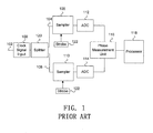
- Figure 1 depicts a traditional timing correction system traditionally used in time sampling oscilloscopes.
- a clock signal 102 synchronized to the data is input into the system 100 through the clock signal input 100.
- the clock signal 102 is split into two clock signals 104 and 106 via a splitter 120.
- Each clock signal 104 and 106 is sent to a respective sampler 108 and 110.
- Samplers 108 and 110 sample the clock signal at different phases that are ideally 90 degrees apart. That is, the samplers 108 and 110 are strobed by a strobe 122 at 90 degrees offset from each other. The samplers are set to strobe at times that are separated by 90 degrees so that the in-phase and quadrature components of the clock signal can be measured.
- the error made in estimating the phase of the clock signal is a function of only the amplitude noise of the clock and noise present in the samplers 108 and 110.
- the output signals from the samplers 108 and 110 are each input into respective analog-to-digital converters (ADC) 112 and 114.
- ADC analog-to-digital converters
- the digitized signals are then sent to the phase measurement unit 116 so the phases of the digitized signals can be calculated.
- a timing correction can be calculated in a processor 118.
- the in-phase and quadrature components of the digitized signal are used to estimate the phase of the clock, and from the phase of the clock the timing error of the sampling test and measurement instrument can be estimated.
- the jitter measured by the scope becomes a function of the phase of the signal. This leads to non-repeatable results where different values or jitter are measured depending on the phase difference between the clock and a measured data signal by the oscilloscope. This causes different parts of the measured data signal to have potentially different amounts of jitter depending on the phase of the clock at the point of the measurement. This is non-ideal and can lead to user confusion.
- Certain embodiments of the disclosed technology include a method for correcting a timing error in a test and measurement instrument.
- the method includes receiving a clock signal that is split into a first clock signal, a second clock signal, a third clock signal and a fourth clock signal.
- the first clock signal is routed to a first sampler
- the second clock signal is routed to a second sampler
- the third clock signal is routed to a third sampler
- the fourth clock signal is routed to the fourth sampler.
- the first clock signal is sampled at the first sampler at a first phase
- the second clock signal is sampled at the second sampler at a second phase that is 90 degrees offset from the first phase
- the third clock signal is sampled at the third sampler at a third phase that is 45 degrees offset from the first phase
- the fourth clock signal is sampled at the fourth sampler at a fourth phase that is 90 degrees offset from the third phase.
- Each of the outputs from the samplers are digitized and a timing correction is calculated based on the digitized outputs from the digitized outputs.
- Timing error correction system for use in a test and measurement instrument.
- the timing error correction system includes a clock input, a splitter configured to split the clock signal into four clock signals; four samplers, each sampler configured to receive one of the four clock signals and configured to output a sampled signal, at least two analog-to-digital converters configured to receive the output sampled signals from the four samplers, and a processor configured to calculate a timing correction error based on the digitized outputs of the four samplers.
- the disclosed technology reduces the amount of jitter in an equivalent time sampling test and measurement instrument.
- the equivalent time system reduces jitter by accurately measuring and then correcting the timing errors of a sampling test and measurement instrument.
- the disclosed technology reduces the amount of error in the time estimation and thereby reduces the total jitter present in a measurement of a data signal, as discussed in more detail below.
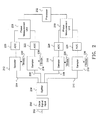
- FIG. 2 depicts some embodiments of the equivalent time system of the disclosed technology.
- the system includes an input 200 for a clock signal 202.
- the clock signal 202 is a sinusoid or similar sine like signal that is aligned to a data signal.
- the clock signal 202 is split into four clock signals 204, 206, 208 and 210.
- the clock signal may be split by using a splitter 234.
- Each of the clock signals 204, 206, 208, and 210 are received at a respective sampler 212, 214, 216, and 218.
- the first set of samplers 212 and 214 are strobed by a strobe 236 to be out of phase by 90 degrees, similar to samplers 108 and 110 in Fig. 1 discussed above.
- the phase delay is added not by delaying the incoming clock signal, but by adjusting the timing of the strobe.
- the phase delay is added by adjusting the timing of the strobe, rather than delaying the incoming clock signal.
- the strobe adjusts when the signal is measured. Because the timing of the strobe is not exact, a small amount of uncertainty is present in the timing of the strobe. The uncertainty causes a divergence from the ideal 90 degrees that is required for the optimal quadrature measurement.
- the second set of samplers 216 and 218 are also strobed by a strobe 236 to be out of phase by 90 degrees with each other.
- the second set of samplers 216 and 218 are strobed with a delay that is offset from the first set of samplers 212 and 214, so that a different portion of the clock signal can be measured. Therefore, sampler 216 is offset from sampler 212 by 45 degrees and sampler 218 is offset from sampler 214 by 45 degrees. Therefore each of the samplers are set to strobe at times separated by 45 degrees. This allows for greater accuracy in determining the timing error by measuring the signal at more phases. By adding the two additional samplers 216 and 218 that have an additional phase adjustment delay with reference to the first set of samplers 212 and 214, the total jitter as well as the variability can be reduced.
- the outputs from each of the samplers 212, 214, 216, and 218 are digitized through respective analog-to-digital converters (ADC) 220, 222, 224, and 226.
- ADC analog-to-digital converters
- the digitized outputs from the first set of samplers 212 and 214 are inputted to a phase measurement unit 228 and the digitized outputs from the second set of samplers 216 and 218 are inputted to a phase measurement unit 230.
- the phase measurement units 228 and 230 may be, for example, processors.
- the phase measurement units 228 and 230 determine the phase difference between samplers 212 and 214, and 216 and 218, respectively.
- phase differences are sent to processor 232 and processor 232 determines the average of the phase differences and calculates a timing correction based on the average.
- the phase measurement units 228 and 230 may be part of the processor 232.
- phase measurement units 228 and 230 can be located in a single processor separate from processor 232.
- the test and measurement instrument uses this correction to correct the timing of the measured data signal. This allows the measured data signal to be placed in the proper order of acquisition.
- Fig. 2 The advantage of the system shown in Fig. 2 is that when the delay is 45 degrees between each of the samplers, the jitter dependence on the phase of the clock is entirely removed. This eliminates the variation and reduces the total jitter by approximately 40%. Although the above system is preferred as it is the most accurate, it requires two additional analog-to-digital converters within the test and measurement instrument.
- Figure 3 depicts an alternative embodiment of the disclosed technology using only two ADCs.
- this system also includes an input 300 for a clock signal 302.
- the clock signal 302 is also split into four clock signals 304, 306, 308 and 310 using a splitter 332.
- Each clock signal 304, 306, 308, and 310 is received by a respective sampler 312, 314, 316, and 318, as discussed above with respect to Fig. 2 .
- each of the samplers are strobed to be out of phase by 45 degrees by a strobe 334.
- the analog output from sampler 312 and the analog output from sampler 316 are summed together by a summer 320, and the analog output from sampler 314 and the analog output from sampler 318 are summed together by a summer 322.
- Each of the outputs from the summers 320 and 322 are then digitally converted by ADCs 324 and 326, respectively.
- the output from the ADCs 324 and 326 are input to the phase measurement unit 328.
- the phase measurement unit 328 determines the phase difference between the output of the summer 320 and the output of the summer 322. Then, a timing correction can be calculated via processor 330. Again, the phase measurement unit 328 may be located within the processor 330.
- the timing error correction system includes a processor and a memory (not shown) to store executable instructions for implementing the above discussed processors of the test and measurement instrument.
- Computer readable code embodied on a computer readable medium, when executed, causes the computer to perform any of the above-described operations.
- a computer is any device that can execute code. Microprocessors, programmable logic devices, multiprocessor systems, digital signal processors, personal computers, or the like are all examples of such a computer.
- the computer readable medium can be a tangible computer readable medium that is configured to store the computer readable code in a non-transitory manner.
- Example embodiments may provide a method for correcting a timing error in a test and measurement instrument, comprising receiving a clock signal, splitting the clock signal into a first clock signal, a second clock signal, a third clock signal, and a fourth clock signal, routing the first clock signal to a first sampler, a second clock signal to a second sampler, a third clock signal to a third sampler, and a fourth clock signal to a fourth sampler, sampling the first clock signal at the first sampler at a first phase, sampling the second clock signal at the second sampler at a second phase that is 90 degrees offset from the first phase, sampling the third clock signal at the third sampler at a third phase that is 45 degrees offset from the first phase, and sampling the fourth clock signal at the fourth sampler at a fourth phase that is 90 degrees offset from the third phase, and digitizing each of the outputs from the samplers and calculating a timing correction based on the digitized outputs from the digitized outputs.
- the outputs from the first sampler and the third sampler are summed, and the outputs from the second sampler and the fourth sampler are summed prior to the digitizing.
- calculating a time correction includes calculating a first phase measurement between the first sampler and the second sampler, calculating a second phase measurement between the third sampler and the fourth sampler, and averaging the first and the second phase measurement.
- Some example embodiments may further include modifying timing of a data signal based on the calculated timing correction.
- Some example embodiments may provide a timing error correction system for use in a test and measurement instrument, comprising a clock signal input configured to receive a clock signal, a splitter configured to split the clock signal into four clock signals, four samplers, each sampler configured to receive one of the four clock signals and configured to output a sampled signal, at least two analog-to-digital converters configured to receive the output sampled signals from the four samplers, and a processor configured to calculate a timing correction error based on the digitized outputs of the four samplers.
- each sampler of the four samplers is strobed to be offset 45 degrees from at least one of the other samplers.
- Some example embodiments may further comprise four analog-to-digital converters, each analog-to-digital converter configured to receive one of the four outputs from the four samplers, wherein the processor is configured to calculate the timing correction error by calculating a first phase measurement between the first sampler and the second sampler, calculating a second phase measurement between the third sampler and the fourth sampler, and averaging the first and the second phase measurement.
- Some example embodiments may further comprise a first summer configured to sum the output from the first sampler and the output from the third sampler, and a second summer configured to sum the output from the second sampler and the output from the fourth sampler, wherein the outputs from the first summer and the second summer are each sent to the at least two analog-to-digital converters.
- the processor is further configured to correct a timing of a data signal based on the calculated timing correction.
Landscapes
- Physics & Mathematics (AREA)
- General Physics & Mathematics (AREA)
- Nonlinear Science (AREA)
- Engineering & Computer Science (AREA)
- General Engineering & Computer Science (AREA)
- Analogue/Digital Conversion (AREA)
- Digital Transmission Methods That Use Modulated Carrier Waves (AREA)
- Stabilization Of Oscillater, Synchronisation, Frequency Synthesizers (AREA)
Abstract
Description
- This disclosure relates to an equivalent time system in a sampling test and measurement instrument to reduce the amount of jitter in a test and measurement instrument. Specifically, the disclosure relates to calculating a timing correction via a clock signal to reduce the amount of jitter in a test and measurement instrument.
- In an equivalent time sampling oscilloscope, a phase reference module is used to compensate for jitter in the time base of the oscilloscope. Two signals are measured - a data signal and a clock signal. The clock signal is a sinusoid or a similar sine-like signal that is aligned to the data signal. The data signal, on the other hand, can be almost any other type of signal. Traditionally, timing errors are calculated by the system shown in
Fig. 1 . The timing correction is made to the data signal by measuring the phase of the clock signal and using the clock signal phase measurement to adjust the timing of the data signal based on the calculated error. -
Figure 1 depicts a traditional timing correction system traditionally used in time sampling oscilloscopes. Aclock signal 102 synchronized to the data is input into thesystem 100 through theclock signal input 100. Theclock signal 102 is split into twoclock signals splitter 120. - Each
clock signal respective sampler samplers strobe 122 at 90 degrees offset from each other. The samplers are set to strobe at times that are separated by 90 degrees so that the in-phase and quadrature components of the clock signal can be measured. When the phase between the two samples taken by thesamplers samplers - The output signals from the
samplers phase measurement unit 116 so the phases of the digitized signals can be calculated. Once the phases have been calculated, a timing correction can be calculated in aprocessor 118. The in-phase and quadrature components of the digitized signal are used to estimate the phase of the clock, and from the phase of the clock the timing error of the sampling test and measurement instrument can be estimated. - Because the actual difference between the two samples is not exactly 90 degrees, the jitter measured by the scope becomes a function of the phase of the signal. This leads to non-repeatable results where different values or jitter are measured depending on the phase difference between the clock and a measured data signal by the oscilloscope. This causes different parts of the measured data signal to have potentially different amounts of jitter depending on the phase of the clock at the point of the measurement. This is non-ideal and can lead to user confusion.
- Certain embodiments of the disclosed technology include a method for correcting a timing error in a test and measurement instrument. The method includes receiving a clock signal that is split into a first clock signal, a second clock signal, a third clock signal and a fourth clock signal. The first clock signal is routed to a first sampler, the second clock signal is routed to a second sampler, the third clock signal is routed to a third sampler; and the fourth clock signal is routed to the fourth sampler. The first clock signal is sampled at the first sampler at a first phase, the second clock signal is sampled at the second sampler at a second phase that is 90 degrees offset from the first phase, the third clock signal is sampled at the third sampler at a third phase that is 45 degrees offset from the first phase, and the fourth clock signal is sampled at the fourth sampler at a fourth phase that is 90 degrees offset from the third phase. Each of the outputs from the samplers are digitized and a timing correction is calculated based on the digitized outputs from the digitized outputs.
- Certain embodiments of the disclosed technology include a timing error correction system for use in a test and measurement instrument. The timing error correction system includes a clock input, a splitter configured to split the clock signal into four clock signals; four samplers, each sampler configured to receive one of the four clock signals and configured to output a sampled signal, at least two analog-to-digital converters configured to receive the output sampled signals from the four samplers, and a processor configured to calculate a timing correction error based on the digitized outputs of the four samplers.
-
-
FIG. 1 illustrates a block diagram of a traditional timing correction system used in a sampling test and measurement instrument. -
FIGS. 2 and3 illustrate block diagrams of embodiments of a timing correction system used in a sampling test and measurement instrument according to the disclosed technology. - In the drawings, which are not necessarily to scale, like or corresponding elements of the disclosed systems and methods are denoted by the same reference numerals.
- The disclosed technology reduces the amount of jitter in an equivalent time sampling test and measurement instrument. The equivalent time system reduces jitter by accurately measuring and then correcting the timing errors of a sampling test and measurement instrument. The disclosed technology reduces the amount of error in the time estimation and thereby reduces the total jitter present in a measurement of a data signal, as discussed in more detail below.
-
Figure 2 depicts some embodiments of the equivalent time system of the disclosed technology. The system includes aninput 200 for aclock signal 202. Theclock signal 202 is a sinusoid or similar sine like signal that is aligned to a data signal. Theclock signal 202 is split into fourclock signals splitter 234. Each of theclock signals respective sampler - The first set of
samplers strobe 236 to be out of phase by 90 degrees, similar tosamplers Fig. 1 discussed above. The phase delay is added not by delaying the incoming clock signal, but by adjusting the timing of the strobe. The phase delay is added by adjusting the timing of the strobe, rather than delaying the incoming clock signal. The strobe adjusts when the signal is measured. Because the timing of the strobe is not exact, a small amount of uncertainty is present in the timing of the strobe. The uncertainty causes a divergence from the ideal 90 degrees that is required for the optimal quadrature measurement. - Therefore, the second set of
samplers strobe 236 to be out of phase by 90 degrees with each other. However, the second set ofsamplers samplers sampler 216 is offset fromsampler 212 by 45 degrees andsampler 218 is offset fromsampler 214 by 45 degrees. Therefore each of the samplers are set to strobe at times separated by 45 degrees. This allows for greater accuracy in determining the timing error by measuring the signal at more phases. By adding the twoadditional samplers samplers - The outputs from each of the
samplers samplers phase measurement unit 228 and the digitized outputs from the second set ofsamplers phase measurement unit 230. Thephase measurement units phase measurement units samplers processor 232 andprocessor 232 determines the average of the phase differences and calculates a timing correction based on the average. Alternatively, thephase measurement units processor 232. Or,phase measurement units processor 232. - Once the timing correction has been determined, the test and measurement instrument uses this correction to correct the timing of the measured data signal. This allows the measured data signal to be placed in the proper order of acquisition.
- The advantage of the system shown in
Fig. 2 is that when the delay is 45 degrees between each of the samplers, the jitter dependence on the phase of the clock is entirely removed. This eliminates the variation and reduces the total jitter by approximately 40%. Although the above system is preferred as it is the most accurate, it requires two additional analog-to-digital converters within the test and measurement instrument. - It may be preferable to use two ADCs to avoid the need for additional analog to digital converters (ADCs).
Figure 3 depicts an alternative embodiment of the disclosed technology using only two ADCs. - As seen in
Fig. 3 , this system also includes aninput 300 for aclock signal 302. Theclock signal 302 is also split into fourclock signals splitter 332. Eachclock signal respective sampler Fig. 2 . Same as with the embodiment discussed with respect toFig. 2 , each of the samplers are strobed to be out of phase by 45 degrees by astrobe 334. - However, rather than the outputs of the
samplers Fig. 2 , the analog output fromsampler 312 and the analog output fromsampler 316 are summed together by asummer 320, and the analog output fromsampler 314 and the analog output fromsampler 318 are summed together by asummer 322. - Each of the outputs from the
summers ADCs ADCs phase measurement unit 328. Thephase measurement unit 328 determines the phase difference between the output of thesummer 320 and the output of thesummer 322. Then, a timing correction can be calculated viaprocessor 330. Again, thephase measurement unit 328 may be located within theprocessor 330. - As mentioned above, the timing error correction system includes a processor and a memory (not shown) to store executable instructions for implementing the above discussed processors of the test and measurement instrument. Computer readable code embodied on a computer readable medium, when executed, causes the computer to perform any of the above-described operations. As used here, a computer is any device that can execute code. Microprocessors, programmable logic devices, multiprocessor systems, digital signal processors, personal computers, or the like are all examples of such a computer. In some embodiments, the computer readable medium can be a tangible computer readable medium that is configured to store the computer readable code in a non-transitory manner.
- Example embodiments may provide a method for correcting a timing error in a test and measurement instrument, comprising receiving a clock signal, splitting the clock signal into a first clock signal, a second clock signal, a third clock signal, and a fourth clock signal, routing the first clock signal to a first sampler, a second clock signal to a second sampler, a third clock signal to a third sampler, and a fourth clock signal to a fourth sampler, sampling the first clock signal at the first sampler at a first phase, sampling the second clock signal at the second sampler at a second phase that is 90 degrees offset from the first phase, sampling the third clock signal at the third sampler at a third phase that is 45 degrees offset from the first phase, and sampling the fourth clock signal at the fourth sampler at a fourth phase that is 90 degrees offset from the third phase, and digitizing each of the outputs from the samplers and calculating a timing correction based on the digitized outputs from the digitized outputs.
- In some example embodiments the outputs from the first sampler and the third sampler are summed, and the outputs from the second sampler and the fourth sampler are summed prior to the digitizing.
- In some example embodiments, calculating a time correction includes calculating a first phase measurement between the first sampler and the second sampler, calculating a second phase measurement between the third sampler and the fourth sampler, and averaging the first and the second phase measurement.
- Some example embodiments may further include modifying timing of a data signal based on the calculated timing correction.
- Some example embodiments may provide a timing error correction system for use in a test and measurement instrument, comprising a clock signal input configured to receive a clock signal, a splitter configured to split the clock signal into four clock signals, four samplers, each sampler configured to receive one of the four clock signals and configured to output a sampled signal, at least two analog-to-digital converters configured to receive the output sampled signals from the four samplers, and a processor configured to calculate a timing correction error based on the digitized outputs of the four samplers.
- In some example embodiments, each sampler of the four samplers is strobed to be offset 45 degrees from at least one of the other samplers.
- Some example embodiments may further comprise four analog-to-digital converters, each analog-to-digital converter configured to receive one of the four outputs from the four samplers, wherein the processor is configured to calculate the timing correction error by calculating a first phase measurement between the first sampler and the second sampler, calculating a second phase measurement between the third sampler and the fourth sampler, and averaging the first and the second phase measurement.
- Some example embodiments may further comprise a first summer configured to sum the output from the first sampler and the output from the third sampler, and a second summer configured to sum the output from the second sampler and the output from the fourth sampler, wherein the outputs from the first summer and the second summer are each sent to the at least two analog-to-digital converters.
- In some example embodiments the processor is further configured to correct a timing of a data signal based on the calculated timing correction.
- Having described and illustrated the principles of the disclosed technology in a preferred embodiment thereof, it should be apparent that the disclosed technology can be modified in arrangement and detail without departing from such principles. We claim all modifications and variations coming within the scope of the following claims.
Claims (9)
- A method for correcting a timing error in a test and measurement instrument, comprising:receiving a clock signal;splitting the clock signal into a first clock signal, a second clock signal, a third clock signal, and a fourth clock signal;routing the first clock signal to a first sampler, a second clock signal to a second sampler, a third clock signal to a third sampler; and a fourth clock signal to a fourth sampler;sampling the first clock signal at the first sampler at a first phase, sampling the second clock signal at the second sampler at a second phase that is 90 degrees offset from the first phase, sampling the third clock signal at the third sampler at a third phase that is 45 degrees offset from the first phase, and sampling the fourth clock signal at the fourth sampler at a fourth phase that is 90 degrees offset from the third phase;digitizing each of the outputs from the samplers; andcalculating a timing correction based on the digitized outputs from the samplers.
- The method of claim 1, wherein the outputs from the first sampler and the third sampler are summed, and the outputs from the second sampler and the fourth sampler are summed prior to the digitizing.
- The method of claim 1 or 2, wherein the calculating a time correction includes:calculating a first phase measurement between the first sampler and the second sampler,calculating a second phase measurement between the third sampler and the fourth sampler, andaveraging the first and the second phase measurement.
- The method of any previous claim, further including modifying timing of a data signal based on the calculated timing correction.
- A timing error correction system for use in a test and measurement instrument, comprising:a clock signal input configured to receive a clock signal;a splitter configured to split the clock signal into four clock signals;four samplers, each sampler configured to receive one of the four clock signals and configured to output a sampled signal;at least two analog-to-digital converters configured to receive the output sampled signals from the four samplers; anda processor configured to calculate a timing correction error based on the digitized outputs of the four samplers.
- The timing error correction system of claim 5, wherein each sampler of the four samplers is strobed to be offset 45 degrees from at least one of the other samplers.
- The timing error correction system of claim 5 or 6, further comprising four analog-to-digital converters, each analog-to-digital converter configured to receive one of the four outputs from the four samplers, wherein the processor is configured to calculate the timing correction error by calculating a first phase measurement between the first sampler and the second sampler, calculating a second phase measurement between the third sampler and the fourth sampler, and averaging the first and the second phase measurement.
- The timing error correction system of any of claims 5 to 7, further comprising:a first summer configured to sum the output from the first sampler and the output from the third sampler;a second summer configured to sum the output from the second sampler and the output from the fourth sampler,wherein the outputs from the first summer and the second summer are each sent to the at least two analog-to-digital converters.
- The timing error correction system of any of claims 5 to 8, wherein the processor is further configured to correct a timing of a data signal based on the calculated timing correction.
Applications Claiming Priority (2)
| Application Number | Priority Date | Filing Date | Title |
|---|---|---|---|
| US201462030214P | 2014-07-29 | 2014-07-29 | |
| US14/519,370 US9909907B2 (en) | 2014-07-29 | 2014-10-21 | Double quadrature with adaptive phase shift for improved phase reference performance |
Publications (2)
| Publication Number | Publication Date |
|---|---|
| EP2985616A2 true EP2985616A2 (en) | 2016-02-17 |
| EP2985616A3 EP2985616A3 (en) | 2016-03-09 |
Family
ID=53762049
Family Applications (1)
| Application Number | Title | Priority Date | Filing Date |
|---|---|---|---|
| EP15178826.2A Withdrawn EP2985616A3 (en) | 2014-07-29 | 2015-07-29 | Double quadrature with adaptive phase shift for improved phase reference performance |
Country Status (4)
| Country | Link |
|---|---|
| US (1) | US9909907B2 (en) |
| EP (1) | EP2985616A3 (en) |
| JP (1) | JP2016031371A (en) |
| CN (1) | CN105319523A (en) |
Families Citing this family (6)
| Publication number | Priority date | Publication date | Assignee | Title |
|---|---|---|---|---|
| US10177778B2 (en) | 2016-12-12 | 2019-01-08 | Rambus Inc. | Phase adjustment for interleaved analog to digital converters |
| US10802074B2 (en) * | 2018-01-02 | 2020-10-13 | Jitterlabs Llc | Method and apparatus for analyzing phase noise in a signal from an electronic device |
| WO2020137657A1 (en) * | 2018-12-25 | 2020-07-02 | 京セラ株式会社 | Analogue/digital converter, wireless communication device, and analogue/digital conversion method |
| CN109581018B (en) * | 2019-01-08 | 2022-02-01 | 北京工业大学 | Time base error synchronous compensation method and device of broadband sampling oscilloscope |
| CN110426974B (en) * | 2019-08-08 | 2024-04-09 | 南京邮电大学 | An equivalent sampling control circuit based on quadrature phase gating |
| CN114460524B (en) * | 2022-02-09 | 2025-07-11 | 马来西亚明试国际有限公司 | Digital pin calibration method and system for automatic test equipment and automatic test equipment |
Family Cites Families (7)
| Publication number | Priority date | Publication date | Assignee | Title |
|---|---|---|---|---|
| US6384657B1 (en) | 2001-03-05 | 2002-05-07 | Tektronix, Inc. | Phase startable clock device having improved stability |
| US6865496B2 (en) * | 2001-11-01 | 2005-03-08 | Agilent Technologies, Inc. | Zero-crossing direction and time interval jitter measurement apparatus using offset sampling |
| US6573761B1 (en) | 2002-04-08 | 2003-06-03 | Agilent Technologies, Inc. | Timebase for sampling an applied signal having a synchronous trigger |
| CN100545919C (en) * | 2003-10-30 | 2009-09-30 | 汤姆森特许公司 | Differential phase detector |
| CN1910939A (en) * | 2004-01-23 | 2007-02-07 | 日出电讯公司 | Method and apparatus for measuring jitter |
| US20120112807A1 (en) * | 2010-11-04 | 2012-05-10 | Tektronix, Inc. | Test and measurement instrument with oscillator phase dejitter |
| CN103529293B (en) * | 2013-09-11 | 2015-09-30 | 西安电子科技大学 | Based on parallel frequency and the cyclical signal measurement method of parameters of rim effect |
-
2014
- 2014-10-21 US US14/519,370 patent/US9909907B2/en not_active Expired - Fee Related
-
2015
- 2015-07-29 EP EP15178826.2A patent/EP2985616A3/en not_active Withdrawn
- 2015-07-29 JP JP2015149994A patent/JP2016031371A/en not_active Abandoned
- 2015-07-29 CN CN201510453820.0A patent/CN105319523A/en active Pending
Non-Patent Citations (1)
| Title |
|---|
| None |
Also Published As
| Publication number | Publication date |
|---|---|
| JP2016031371A (en) | 2016-03-07 |
| EP2985616A3 (en) | 2016-03-09 |
| CN105319523A (en) | 2016-02-10 |
| US9909907B2 (en) | 2018-03-06 |
| US20160033309A1 (en) | 2016-02-04 |
Similar Documents
| Publication | Publication Date | Title |
|---|---|---|
| US9909907B2 (en) | Double quadrature with adaptive phase shift for improved phase reference performance | |
| US6269317B1 (en) | Self-calibration of an oscilloscope using a square-wave test signal | |
| US20060250288A1 (en) | System and method for timing calibration of time-interleaved data converters | |
| WO2020028314A1 (en) | Current sensor configuration and calibration | |
| CN108494402A (en) | A kind of TIADC systematic error estimations and compensation method based on Sine-Fitting | |
| US11874312B1 (en) | Phase noise measurement method and measurement system | |
| US7825839B2 (en) | Measuring device and measuring method for measuring the power of a high-frequency signal | |
| EP3121611A1 (en) | Time corrected time-domain reflectometer | |
| CN104467927A (en) | Method and device for compensating phases of receive channel | |
| US20160182076A1 (en) | Background Calibration for Digital-to-Analog Converters | |
| KR101423653B1 (en) | Measuring apparatus and measuring method | |
| KR100991938B1 (en) | Synchronous Phaser Measurement Modules, Devices, and Methods | |
| US10955441B2 (en) | Measurement system and method for operating a measurement system | |
| US10797624B2 (en) | Rotation angle correction device and motor control system | |
| US8482444B1 (en) | Calibration of analog-to-digital converter data capture | |
| RU2680091C1 (en) | Global navigation satellite systems signals simulators calibration method | |
| US7450043B2 (en) | Method of compensating for deterministic jitter due to interleave error | |
| EP2450714A2 (en) | Test and measurement instrument with oscillator phase dejitter | |
| GB2523225A (en) | Signal timing | |
| KR101191880B1 (en) | Signal measuring apparatus and method therof | |
| US8866517B2 (en) | Power system data acquisition systems | |
| US8843615B2 (en) | Method and device for measuring the temporal drift of an item of electronic equipment connected to a network | |
| KR101022358B1 (en) | Least Squares Digital Frequency Discrimination Device and Method for Phase Compensation Based Environment | |
| KR100860711B1 (en) | Line voltage measurement method using interpolation method | |
| CN106885932A (en) | A kind of oscillograph and its ADC uniformity compensation methods |
Legal Events
| Date | Code | Title | Description |
|---|---|---|---|
| PUAL | Search report despatched |
Free format text: ORIGINAL CODE: 0009013 |
|
| PUAI | Public reference made under article 153(3) epc to a published international application that has entered the european phase |
Free format text: ORIGINAL CODE: 0009012 |
|
| AK | Designated contracting states |
Kind code of ref document: A2 Designated state(s): AL AT BE BG CH CY CZ DE DK EE ES FI FR GB GR HR HU IE IS IT LI LT LU LV MC MK MT NL NO PL PT RO RS SE SI SK SM TR |
|
| AX | Request for extension of the european patent |
Extension state: BA ME |
|
| AK | Designated contracting states |
Kind code of ref document: A3 Designated state(s): AL AT BE BG CH CY CZ DE DK EE ES FI FR GB GR HR HU IE IS IT LI LT LU LV MC MK MT NL NO PL PT RO RS SE SI SK SM TR |
|
| AX | Request for extension of the european patent |
Extension state: BA ME |
|
| RIC1 | Information provided on ipc code assigned before grant |
Ipc: H03L 7/00 20060101ALI20160201BHEP Ipc: G01R 13/02 20060101ALI20160201BHEP Ipc: G01R 31/317 20060101AFI20160201BHEP |
|
| 17P | Request for examination filed |
Effective date: 20160902 |
|
| RBV | Designated contracting states (corrected) |
Designated state(s): AL AT BE BG CH CY CZ DE DK EE ES FI FR GB GR HR HU IE IS IT LI LT LU LV MC MK MT NL NO PL PT RO RS SE SI SK SM TR |
|
| GRAP | Despatch of communication of intention to grant a patent |
Free format text: ORIGINAL CODE: EPIDOSNIGR1 |
|
| RIC1 | Information provided on ipc code assigned before grant |
Ipc: G01R 31/317 20060101ALI20190214BHEP Ipc: G01D 18/00 20060101AFI20190214BHEP Ipc: G01R 13/02 20060101ALI20190214BHEP |
|
| INTG | Intention to grant announced |
Effective date: 20190304 |
|
| RIN1 | Information on inventor provided before grant (corrected) |
Inventor name: PEETERS WEEM, JAN Inventor name: ENGENHARDT, KLAUS Inventor name: DOBOS, LASZLO |
|
| STAA | Information on the status of an ep patent application or granted ep patent |
Free format text: STATUS: THE APPLICATION IS DEEMED TO BE WITHDRAWN |
|
| 18D | Application deemed to be withdrawn |
Effective date: 20190716 |