EP2984152B1 - Organic electroluminescent device - Google Patents
Organic electroluminescent device Download PDFInfo
- Publication number
- EP2984152B1 EP2984152B1 EP14711162.9A EP14711162A EP2984152B1 EP 2984152 B1 EP2984152 B1 EP 2984152B1 EP 14711162 A EP14711162 A EP 14711162A EP 2984152 B1 EP2984152 B1 EP 2984152B1
- Authority
- EP
- European Patent Office
- Prior art keywords
- group
- aromatic
- electron
- substituted
- atoms
- Prior art date
- Legal status (The legal status is an assumption and is not a legal conclusion. Google has not performed a legal analysis and makes no representation as to the accuracy of the status listed.)
- Active
Links
- 125000003118 aryl group Chemical group 0.000 claims description 130
- 150000001875 compounds Chemical class 0.000 claims description 92
- 239000000463 material Substances 0.000 claims description 62
- 150000003254 radicals Chemical class 0.000 claims description 56
- 238000004768 lowest unoccupied molecular orbital Methods 0.000 claims description 52
- 238000004770 highest occupied molecular orbital Methods 0.000 claims description 44
- 125000004432 carbon atom Chemical group C* 0.000 claims description 43
- -1 aromatic phosphine oxides Chemical class 0.000 claims description 35
- 229910052799 carbon Inorganic materials 0.000 claims description 32
- 125000001424 substituent group Chemical group 0.000 claims description 29
- 229910052760 oxygen Inorganic materials 0.000 claims description 27
- 229910052731 fluorine Inorganic materials 0.000 claims description 26
- 239000011159 matrix material Substances 0.000 claims description 24
- 229910052717 sulfur Inorganic materials 0.000 claims description 23
- 125000001072 heteroaryl group Chemical group 0.000 claims description 21
- 229910052751 metal Inorganic materials 0.000 claims description 21
- 239000002184 metal Substances 0.000 claims description 21
- 229910052801 chlorine Inorganic materials 0.000 claims description 20
- 229910052794 bromium Inorganic materials 0.000 claims description 19
- 238000000034 method Methods 0.000 claims description 19
- 125000000217 alkyl group Chemical group 0.000 claims description 17
- 229910052740 iodine Inorganic materials 0.000 claims description 17
- 238000002347 injection Methods 0.000 claims description 16
- 239000007924 injection Substances 0.000 claims description 16
- 229910052739 hydrogen Inorganic materials 0.000 claims description 14
- 229910052805 deuterium Inorganic materials 0.000 claims description 13
- UHOVQNZJYSORNB-UHFFFAOYSA-N Benzene Chemical compound C1=CC=CC=C1 UHOVQNZJYSORNB-UHFFFAOYSA-N 0.000 claims description 12
- 125000003545 alkoxy group Chemical group 0.000 claims description 12
- MWPLVEDNUUSJAV-UHFFFAOYSA-N anthracene Chemical compound C1=CC=CC2=CC3=CC=CC=C3C=C21 MWPLVEDNUUSJAV-UHFFFAOYSA-N 0.000 claims description 12
- 125000004435 hydrogen atom Chemical group [H]* 0.000 claims description 11
- JUJWROOIHBZHMG-UHFFFAOYSA-N Pyridine Chemical compound C1=CC=NC=C1 JUJWROOIHBZHMG-UHFFFAOYSA-N 0.000 claims description 10
- 229910052757 nitrogen Inorganic materials 0.000 claims description 10
- 125000006165 cyclic alkyl group Chemical group 0.000 claims description 9
- 125000004001 thioalkyl group Chemical group 0.000 claims description 9
- YTPLMLYBLZKORZ-UHFFFAOYSA-N Thiophene Chemical compound C=1C=CSC=1 YTPLMLYBLZKORZ-UHFFFAOYSA-N 0.000 claims description 8
- YNPNZTXNASCQKK-UHFFFAOYSA-N phenanthrene Chemical compound C1=CC=C2C3=CC=CC=C3C=CC2=C1 YNPNZTXNASCQKK-UHFFFAOYSA-N 0.000 claims description 8
- BBEAQIROQSPTKN-UHFFFAOYSA-N pyrene Chemical compound C1=CC=C2C=CC3=CC=CC4=CC=C1C2=C43 BBEAQIROQSPTKN-UHFFFAOYSA-N 0.000 claims description 8
- 125000001931 aliphatic group Chemical group 0.000 claims description 7
- 125000003342 alkenyl group Chemical group 0.000 claims description 7
- 239000000203 mixture Substances 0.000 claims description 7
- 125000002950 monocyclic group Chemical group 0.000 claims description 7
- 150000002894 organic compounds Chemical class 0.000 claims description 7
- 125000003367 polycyclic group Chemical group 0.000 claims description 7
- 229910052710 silicon Inorganic materials 0.000 claims description 7
- JYEUMXHLPRZUAT-UHFFFAOYSA-N 1,2,3-triazine Chemical compound C1=CN=NN=C1 JYEUMXHLPRZUAT-UHFFFAOYSA-N 0.000 claims description 6
- FCEHBMOGCRZNNI-UHFFFAOYSA-N 1-benzothiophene Chemical compound C1=CC=C2SC=CC2=C1 FCEHBMOGCRZNNI-UHFFFAOYSA-N 0.000 claims description 6
- YLQBMQCUIZJEEH-UHFFFAOYSA-N Furan Chemical compound C=1C=COC=1 YLQBMQCUIZJEEH-UHFFFAOYSA-N 0.000 claims description 6
- SIKJAQJRHWYJAI-UHFFFAOYSA-N Indole Chemical compound C1=CC=C2NC=CC2=C1 SIKJAQJRHWYJAI-UHFFFAOYSA-N 0.000 claims description 6
- KYQCOXFCLRTKLS-UHFFFAOYSA-N Pyrazine Chemical compound C1=CN=CC=N1 KYQCOXFCLRTKLS-UHFFFAOYSA-N 0.000 claims description 6
- KAESVJOAVNADME-UHFFFAOYSA-N Pyrrole Chemical compound C=1C=CNC=1 KAESVJOAVNADME-UHFFFAOYSA-N 0.000 claims description 6
- 150000008365 aromatic ketones Chemical class 0.000 claims description 6
- 125000002915 carbonyl group Chemical group [*:2]C([*:1])=O 0.000 claims description 6
- GVEPBJHOBDJJJI-UHFFFAOYSA-N fluoranthrene Natural products C1=CC(C2=CC=CC=C22)=C3C2=CC=CC3=C1 GVEPBJHOBDJJJI-UHFFFAOYSA-N 0.000 claims description 6
- IMKMFBIYHXBKRX-UHFFFAOYSA-M lithium;quinoline-2-carboxylate Chemical compound [Li+].C1=CC=CC2=NC(C(=O)[O-])=CC=C21 IMKMFBIYHXBKRX-UHFFFAOYSA-M 0.000 claims description 6
- 238000007639 printing Methods 0.000 claims description 6
- 239000000126 substance Substances 0.000 claims description 6
- YJTKZCDBKVTVBY-UHFFFAOYSA-N 1,3-Diphenylbenzene Chemical group C1=CC=CC=C1C1=CC=CC(C=2C=CC=CC=2)=C1 YJTKZCDBKVTVBY-UHFFFAOYSA-N 0.000 claims description 5
- LPHIYKWSEYTCLW-UHFFFAOYSA-N 1h-azaborole Chemical class N1B=CC=C1 LPHIYKWSEYTCLW-UHFFFAOYSA-N 0.000 claims description 5
- 229910052782 aluminium Inorganic materials 0.000 claims description 5
- 125000004104 aryloxy group Chemical group 0.000 claims description 5
- 239000004305 biphenyl Substances 0.000 claims description 5
- 150000001716 carbazoles Chemical class 0.000 claims description 5
- 125000005553 heteroaryloxy group Chemical group 0.000 claims description 5
- VVVPGLRKXQSQSZ-UHFFFAOYSA-N indolo[3,2-c]carbazole Chemical compound C1=CC=CC2=NC3=C4C5=CC=CC=C5N=C4C=CC3=C21 VVVPGLRKXQSQSZ-UHFFFAOYSA-N 0.000 claims description 5
- 150000002642 lithium compounds Chemical class 0.000 claims description 5
- 238000004519 manufacturing process Methods 0.000 claims description 5
- 125000004433 nitrogen atom Chemical group N* 0.000 claims description 5
- 239000000243 solution Substances 0.000 claims description 5
- 238000000859 sublimation Methods 0.000 claims description 5
- 230000008022 sublimation Effects 0.000 claims description 5
- DXBHBZVCASKNBY-UHFFFAOYSA-N 1,2-Benz(a)anthracene Chemical compound C1=CC=C2C3=CC4=CC=CC=C4C=C3C=CC2=C1 DXBHBZVCASKNBY-UHFFFAOYSA-N 0.000 claims description 4
- PCNDJXKNXGMECE-UHFFFAOYSA-N Phenazine Natural products C1=CC=CC2=NC3=CC=CC=C3N=C21 PCNDJXKNXGMECE-UHFFFAOYSA-N 0.000 claims description 4
- 150000001340 alkali metals Chemical class 0.000 claims description 4
- 125000000304 alkynyl group Chemical group 0.000 claims description 4
- 125000003710 aryl alkyl group Chemical group 0.000 claims description 4
- 125000004475 heteroaralkyl group Chemical group 0.000 claims description 4
- WUNJCKOTXFSWBK-UHFFFAOYSA-N indeno[2,1-a]carbazole Chemical compound C1=CC=C2C=C3C4=NC5=CC=CC=C5C4=CC=C3C2=C1 WUNJCKOTXFSWBK-UHFFFAOYSA-N 0.000 claims description 4
- 229960005544 indolocarbazole Drugs 0.000 claims description 4
- 229930192474 thiophene Natural products 0.000 claims description 4
- 229910052721 tungsten Inorganic materials 0.000 claims description 4
- 229910052720 vanadium Inorganic materials 0.000 claims description 4
- 125000001637 1-naphthyl group Chemical group [H]C1=C([H])C([H])=C2C(*)=C([H])C([H])=C([H])C2=C1[H] 0.000 claims description 3
- 125000001622 2-naphthyl group Chemical group [H]C1=C([H])C([H])=C2C([H])=C(*)C([H])=C([H])C2=C1[H] 0.000 claims description 3
- SLGBZMMZGDRARJ-UHFFFAOYSA-N Triphenylene Natural products C1=CC=C2C3=CC=CC=C3C3=CC=CC=C3C2=C1 SLGBZMMZGDRARJ-UHFFFAOYSA-N 0.000 claims description 3
- 150000001491 aromatic compounds Chemical class 0.000 claims description 3
- RFRXIWQYSOIBDI-UHFFFAOYSA-N benzarone Chemical compound CCC=1OC2=CC=CC=C2C=1C(=O)C1=CC=C(O)C=C1 RFRXIWQYSOIBDI-UHFFFAOYSA-N 0.000 claims description 3
- 229910052790 beryllium Inorganic materials 0.000 claims description 3
- 125000000609 carbazolyl group Chemical group C1(=CC=CC=2C3=CC=CC=C3NC12)* 0.000 claims description 3
- 239000012159 carrier gas Substances 0.000 claims description 3
- PZOUSPYUWWUPPK-UHFFFAOYSA-N indole Natural products CC1=CC=CC2=C1C=CN2 PZOUSPYUWWUPPK-UHFFFAOYSA-N 0.000 claims description 3
- RKJUIXBNRJVNHR-UHFFFAOYSA-N indolenine Natural products C1=CC=C2CC=NC2=C1 RKJUIXBNRJVNHR-UHFFFAOYSA-N 0.000 claims description 3
- 150000003951 lactams Chemical class 0.000 claims description 3
- 125000004437 phosphorous atom Chemical group 0.000 claims description 3
- PBMFSQRYOILNGV-UHFFFAOYSA-N pyridazine Chemical compound C1=CC=NN=C1 PBMFSQRYOILNGV-UHFFFAOYSA-N 0.000 claims description 3
- 150000003230 pyrimidines Chemical class 0.000 claims description 3
- 238000004528 spin coating Methods 0.000 claims description 3
- 150000003918 triazines Chemical class 0.000 claims description 3
- 125000005580 triphenylene group Chemical group 0.000 claims description 3
- 238000001947 vapour-phase growth Methods 0.000 claims description 3
- 229910052725 zinc Inorganic materials 0.000 claims description 3
- 125000000520 N-substituted aminocarbonyl group Chemical group [*]NC(=O)* 0.000 claims description 2
- 229910001515 alkali metal fluoride Inorganic materials 0.000 claims description 2
- 229910001618 alkaline earth metal fluoride Inorganic materials 0.000 claims description 2
- 150000007859 azaphosphole derivatives Chemical class 0.000 claims description 2
- 125000003785 benzimidazolyl group Chemical class N1=C(NC2=C1C=CC=C2)* 0.000 claims description 2
- 150000004649 carbonic acid derivatives Chemical class 0.000 claims description 2
- 125000004093 cyano group Chemical group *C#N 0.000 claims description 2
- 230000002950 deficient Effects 0.000 claims description 2
- 150000003252 quinoxalines Chemical class 0.000 claims description 2
- 238000005092 sublimation method Methods 0.000 claims description 2
- 238000000926 separation method Methods 0.000 claims 2
- 125000005240 diheteroarylamino group Chemical group 0.000 claims 1
- 239000010410 layer Substances 0.000 description 134
- 0 *c1nc(*)nc(*)n1 Chemical compound *c1nc(*)nc(*)n1 0.000 description 16
- 125000004122 cyclic group Chemical group 0.000 description 13
- 150000002739 metals Chemical class 0.000 description 12
- 101100533558 Mus musculus Sipa1 gene Proteins 0.000 description 11
- ZUOUZKKEUPVFJK-UHFFFAOYSA-N diphenyl Chemical compound C1=CC=CC=C1C1=CC=CC=C1 ZUOUZKKEUPVFJK-UHFFFAOYSA-N 0.000 description 8
- 230000005284 excitation Effects 0.000 description 8
- BASFCYQUMIYNBI-UHFFFAOYSA-N platinum Chemical compound [Pt] BASFCYQUMIYNBI-UHFFFAOYSA-N 0.000 description 8
- 238000003077 quantum chemistry computational method Methods 0.000 description 8
- 230000003111 delayed effect Effects 0.000 description 7
- 229910052741 iridium Inorganic materials 0.000 description 7
- GEQBRULPNIVQPP-UHFFFAOYSA-N 2-[3,5-bis(1-phenylbenzimidazol-2-yl)phenyl]-1-phenylbenzimidazole Chemical compound C1=CC=CC=C1N1C2=CC=CC=C2N=C1C1=CC(C=2N(C3=CC=CC=C3N=2)C=2C=CC=CC=2)=CC(C=2N(C3=CC=CC=C3N=2)C=2C=CC=CC=2)=C1 GEQBRULPNIVQPP-UHFFFAOYSA-N 0.000 description 6
- 125000005842 heteroatom Chemical group 0.000 description 6
- 230000005525 hole transport Effects 0.000 description 6
- GKOZUEZYRPOHIO-UHFFFAOYSA-N iridium atom Chemical compound [Ir] GKOZUEZYRPOHIO-UHFFFAOYSA-N 0.000 description 6
- 239000000758 substrate Substances 0.000 description 6
- 150000001556 benzimidazoles Chemical class 0.000 description 5
- 230000000903 blocking effect Effects 0.000 description 5
- 239000011368 organic material Substances 0.000 description 5
- MPQXHAGKBWFSNV-UHFFFAOYSA-N oxidophosphanium Chemical class [PH3]=O MPQXHAGKBWFSNV-UHFFFAOYSA-N 0.000 description 5
- 125000001997 phenyl group Chemical group [H]C1=C([H])C([H])=C(*)C([H])=C1[H] 0.000 description 5
- 229910052697 platinum Inorganic materials 0.000 description 5
- OWPJBAYCIXEHFA-UHFFFAOYSA-N 1-phenyl-3-(3-phenylphenyl)benzene Chemical compound C1=CC=CC=C1C1=CC=CC(C=2C=C(C=CC=2)C=2C=CC=CC=2)=C1 OWPJBAYCIXEHFA-UHFFFAOYSA-N 0.000 description 4
- UJOBWOGCFQCDNV-UHFFFAOYSA-N 9H-carbazole Chemical compound C1=CC=C2C3=CC=CC=C3NC2=C1 UJOBWOGCFQCDNV-UHFFFAOYSA-N 0.000 description 4
- UFWIBTONFRDIAS-UHFFFAOYSA-N Naphthalene Chemical compound C1=CC=CC2=CC=CC=C21 UFWIBTONFRDIAS-UHFFFAOYSA-N 0.000 description 4
- CZPWVGJYEJSRLH-UHFFFAOYSA-N Pyrimidine Chemical compound C1=CN=CN=C1 CZPWVGJYEJSRLH-UHFFFAOYSA-N 0.000 description 4
- SMWDFEZZVXVKRB-UHFFFAOYSA-N Quinoline Chemical compound N1=CC=CC2=CC=CC=C21 SMWDFEZZVXVKRB-UHFFFAOYSA-N 0.000 description 4
- 229910052784 alkaline earth metal Inorganic materials 0.000 description 4
- 235000010290 biphenyl Nutrition 0.000 description 4
- TXCDCPKCNAJMEE-UHFFFAOYSA-N dibenzofuran Chemical compound C1=CC=C2C3=CC=CC=C3OC2=C1 TXCDCPKCNAJMEE-UHFFFAOYSA-N 0.000 description 4
- IYYZUPMFVPLQIF-UHFFFAOYSA-N dibenzothiophene Chemical compound C1=CC=C2C3=CC=CC=C3SC2=C1 IYYZUPMFVPLQIF-UHFFFAOYSA-N 0.000 description 4
- 239000002019 doping agent Substances 0.000 description 4
- AWJUIBRHMBBTKR-UHFFFAOYSA-N isoquinoline Chemical compound C1=NC=CC2=CC=CC=C21 AWJUIBRHMBBTKR-UHFFFAOYSA-N 0.000 description 4
- 238000005259 measurement Methods 0.000 description 4
- 229910052709 silver Inorganic materials 0.000 description 4
- YAVCXSHORWKJQQ-UHFFFAOYSA-N 1-phenyl-2-(2-phenylphenyl)benzene Chemical compound C1=CC=CC=C1C1=CC=CC=C1C1=CC=CC=C1C1=CC=CC=C1 YAVCXSHORWKJQQ-UHFFFAOYSA-N 0.000 description 3
- 238000000862 absorption spectrum Methods 0.000 description 3
- 150000001342 alkaline earth metals Chemical class 0.000 description 3
- 229940058303 antinematodal benzimidazole derivative Drugs 0.000 description 3
- QVGXLLKOCUKJST-UHFFFAOYSA-N atomic oxygen Chemical compound [O] QVGXLLKOCUKJST-UHFFFAOYSA-N 0.000 description 3
- 239000011248 coating agent Substances 0.000 description 3
- 238000000576 coating method Methods 0.000 description 3
- 239000004020 conductor Substances 0.000 description 3
- RAXXELZNTBOGNW-UHFFFAOYSA-N imidazole Natural products C1=CNC=N1 RAXXELZNTBOGNW-UHFFFAOYSA-N 0.000 description 3
- 239000011229 interlayer Substances 0.000 description 3
- 150000002576 ketones Chemical class 0.000 description 3
- 238000004020 luminiscence type Methods 0.000 description 3
- 239000001301 oxygen Substances 0.000 description 3
- GPRIERYVMZVKTC-UHFFFAOYSA-N p-quaterphenyl Chemical compound C1=CC=CC=C1C1=CC=C(C=2C=CC(=CC=2)C=2C=CC=CC=2)C=C1 GPRIERYVMZVKTC-UHFFFAOYSA-N 0.000 description 3
- 150000003057 platinum Chemical class 0.000 description 3
- ICPSWZFVWAPUKF-UHFFFAOYSA-N 1,1'-spirobi[fluorene] Chemical compound C1=CC=C2C=C3C4(C=5C(C6=CC=CC=C6C=5)=CC=C4)C=CC=C3C2=C1 ICPSWZFVWAPUKF-UHFFFAOYSA-N 0.000 description 2
- JIHQDMXYYFUGFV-UHFFFAOYSA-N 1,3,5-triazine Chemical compound C1=NC=NC=N1 JIHQDMXYYFUGFV-UHFFFAOYSA-N 0.000 description 2
- WJFKNYWRSNBZNX-UHFFFAOYSA-N 10H-phenothiazine Chemical compound C1=CC=C2NC3=CC=CC=C3SC2=C1 WJFKNYWRSNBZNX-UHFFFAOYSA-N 0.000 description 2
- TZMSYXZUNZXBOL-UHFFFAOYSA-N 10H-phenoxazine Chemical compound C1=CC=C2NC3=CC=CC=C3OC2=C1 TZMSYXZUNZXBOL-UHFFFAOYSA-N 0.000 description 2
- KDCGOANMDULRCW-UHFFFAOYSA-N 7H-purine Chemical compound N1=CNC2=NC=NC2=C1 KDCGOANMDULRCW-UHFFFAOYSA-N 0.000 description 2
- DZBUGLKDJFMEHC-UHFFFAOYSA-N acridine Chemical compound C1=CC=CC2=CC3=CC=CC=C3N=C21 DZBUGLKDJFMEHC-UHFFFAOYSA-N 0.000 description 2
- 229910052783 alkali metal Inorganic materials 0.000 description 2
- 229910045601 alloy Inorganic materials 0.000 description 2
- 239000000956 alloy Substances 0.000 description 2
- 229910052788 barium Inorganic materials 0.000 description 2
- IOJUPLGTWVMSFF-UHFFFAOYSA-N benzothiazole Chemical compound C1=CC=C2SC=NC2=C1 IOJUPLGTWVMSFF-UHFFFAOYSA-N 0.000 description 2
- 230000015572 biosynthetic process Effects 0.000 description 2
- 238000004364 calculation method Methods 0.000 description 2
- 150000001721 carbon Chemical group 0.000 description 2
- WDECIBYCCFPHNR-UHFFFAOYSA-N chrysene Chemical compound C1=CC=CC2=CC=C3C4=CC=CC=C4C=CC3=C21 WDECIBYCCFPHNR-UHFFFAOYSA-N 0.000 description 2
- 230000007423 decrease Effects 0.000 description 2
- 238000001194 electroluminescence spectrum Methods 0.000 description 2
- 230000005281 excited state Effects 0.000 description 2
- 230000001747 exhibiting effect Effects 0.000 description 2
- RMBPEFMHABBEKP-UHFFFAOYSA-N fluorene Chemical compound C1=CC=C2C3=C[CH]C=CC3=CC2=C1 RMBPEFMHABBEKP-UHFFFAOYSA-N 0.000 description 2
- 239000011521 glass Substances 0.000 description 2
- 230000005283 ground state Effects 0.000 description 2
- AMGQUBHHOARCQH-UHFFFAOYSA-N indium;oxotin Chemical compound [In].[Sn]=O AMGQUBHHOARCQH-UHFFFAOYSA-N 0.000 description 2
- 238000007641 inkjet printing Methods 0.000 description 2
- 229910052749 magnesium Inorganic materials 0.000 description 2
- 229910001092 metal group alloy Inorganic materials 0.000 description 2
- 125000002496 methyl group Chemical group [H]C([H])([H])* 0.000 description 2
- 125000001624 naphthyl group Chemical group 0.000 description 2
- NIHNNTQXNPWCJQ-UHFFFAOYSA-N o-biphenylenemethane Natural products C1=CC=C2CC3=CC=CC=C3C2=C1 NIHNNTQXNPWCJQ-UHFFFAOYSA-N 0.000 description 2
- 125000002524 organometallic group Chemical group 0.000 description 2
- RDOWQLZANAYVLL-UHFFFAOYSA-N phenanthridine Chemical compound C1=CC=C2C3=CC=CC=C3C=NC2=C1 RDOWQLZANAYVLL-UHFFFAOYSA-N 0.000 description 2
- 229950000688 phenothiazine Drugs 0.000 description 2
- 229910052698 phosphorus Inorganic materials 0.000 description 2
- 238000005424 photoluminescence Methods 0.000 description 2
- 229920000642 polymer Polymers 0.000 description 2
- UMJSCPRVCHMLSP-UHFFFAOYSA-N pyridine Natural products COC1=CC=CN=C1 UMJSCPRVCHMLSP-UHFFFAOYSA-N 0.000 description 2
- XSCHRSMBECNVNS-UHFFFAOYSA-N quinoxaline Chemical compound N1=CC=NC2=CC=CC=C21 XSCHRSMBECNVNS-UHFFFAOYSA-N 0.000 description 2
- 230000005855 radiation Effects 0.000 description 2
- 239000004065 semiconductor Substances 0.000 description 2
- 101150073162 spa1 gene Proteins 0.000 description 2
- 238000001228 spectrum Methods 0.000 description 2
- 125000005259 triarylamine group Chemical group 0.000 description 2
- 239000011701 zinc Substances 0.000 description 2
- FIARMZDBEGVMLV-UHFFFAOYSA-N 1,1,2,2,2-pentafluoroethanolate Chemical group [O-]C(F)(F)C(F)(F)F FIARMZDBEGVMLV-UHFFFAOYSA-N 0.000 description 1
- HQDYNFWTFJFEPR-UHFFFAOYSA-N 1,2,3,3a-tetrahydropyrene Chemical compound C1=C2CCCC(C=C3)C2=C2C3=CC=CC2=C1 HQDYNFWTFJFEPR-UHFFFAOYSA-N 0.000 description 1
- ZFXBERJDEUDDMX-UHFFFAOYSA-N 1,2,3,5-tetrazine Chemical compound C1=NC=NN=N1 ZFXBERJDEUDDMX-UHFFFAOYSA-N 0.000 description 1
- FNQJDLTXOVEEFB-UHFFFAOYSA-N 1,2,3-benzothiadiazole Chemical compound C1=CC=C2SN=NC2=C1 FNQJDLTXOVEEFB-UHFFFAOYSA-N 0.000 description 1
- UGUHFDPGDQDVGX-UHFFFAOYSA-N 1,2,3-thiadiazole Chemical compound C1=CSN=N1 UGUHFDPGDQDVGX-UHFFFAOYSA-N 0.000 description 1
- HTJMXYRLEDBSLT-UHFFFAOYSA-N 1,2,4,5-tetrazine Chemical compound C1=NN=CN=N1 HTJMXYRLEDBSLT-UHFFFAOYSA-N 0.000 description 1
- BBVIDBNAYOIXOE-UHFFFAOYSA-N 1,2,4-oxadiazole Chemical compound C=1N=CON=1 BBVIDBNAYOIXOE-UHFFFAOYSA-N 0.000 description 1
- YGTAZGSLCXNBQL-UHFFFAOYSA-N 1,2,4-thiadiazole Chemical compound C=1N=CSN=1 YGTAZGSLCXNBQL-UHFFFAOYSA-N 0.000 description 1
- FYADHXFMURLYQI-UHFFFAOYSA-N 1,2,4-triazine Chemical compound C1=CN=NC=N1 FYADHXFMURLYQI-UHFFFAOYSA-N 0.000 description 1
- UDGKZGLPXCRRAM-UHFFFAOYSA-N 1,2,5-thiadiazole Chemical compound C=1C=NSN=1 UDGKZGLPXCRRAM-UHFFFAOYSA-N 0.000 description 1
- UUSUFQUCLACDTA-UHFFFAOYSA-N 1,2-dihydropyrene Chemical compound C1=CC=C2C=CC3=CCCC4=CC=C1C2=C43 UUSUFQUCLACDTA-UHFFFAOYSA-N 0.000 description 1
- FKASFBLJDCHBNZ-UHFFFAOYSA-N 1,3,4-oxadiazole Chemical compound C1=NN=CO1 FKASFBLJDCHBNZ-UHFFFAOYSA-N 0.000 description 1
- MBIZXFATKUQOOA-UHFFFAOYSA-N 1,3,4-thiadiazole Chemical compound C1=NN=CS1 MBIZXFATKUQOOA-UHFFFAOYSA-N 0.000 description 1
- BCMCBBGGLRIHSE-UHFFFAOYSA-N 1,3-benzoxazole Chemical compound C1=CC=C2OC=NC2=C1 BCMCBBGGLRIHSE-UHFFFAOYSA-N 0.000 description 1
- FLBAYUMRQUHISI-UHFFFAOYSA-N 1,8-naphthyridine Chemical compound N1=CC=CC2=CC=CN=C21 FLBAYUMRQUHISI-UHFFFAOYSA-N 0.000 description 1
- QWENRTYMTSOGBR-UHFFFAOYSA-N 1H-1,2,3-Triazole Chemical compound C=1C=NNN=1 QWENRTYMTSOGBR-UHFFFAOYSA-N 0.000 description 1
- HYZJCKYKOHLVJF-UHFFFAOYSA-N 1H-benzimidazole Chemical compound C1=CC=C2NC=NC2=C1 HYZJCKYKOHLVJF-UHFFFAOYSA-N 0.000 description 1
- BAXOFTOLAUCFNW-UHFFFAOYSA-N 1H-indazole Chemical compound C1=CC=C2C=NNC2=C1 BAXOFTOLAUCFNW-UHFFFAOYSA-N 0.000 description 1
- USYCQABRSUEURP-UHFFFAOYSA-N 1h-benzo[f]benzimidazole Chemical compound C1=CC=C2C=C(NC=N3)C3=CC2=C1 USYCQABRSUEURP-UHFFFAOYSA-N 0.000 description 1
- JUUZQMUWOVDZSD-UHFFFAOYSA-N 1h-imidazole;pyrazine Chemical compound C1=CNC=N1.C1=CN=CC=N1 JUUZQMUWOVDZSD-UHFFFAOYSA-N 0.000 description 1
- IGHOZKDBCCFNNC-UHFFFAOYSA-N 1h-imidazole;quinoxaline Chemical compound C1=CNC=N1.N1=CC=NC2=CC=CC=C21 IGHOZKDBCCFNNC-UHFFFAOYSA-N 0.000 description 1
- 125000004793 2,2,2-trifluoroethoxy group Chemical group FC(CO*)(F)F 0.000 description 1
- 125000004206 2,2,2-trifluoroethyl group Chemical group [H]C([H])(*)C(F)(F)F 0.000 description 1
- PFRPMHBYYJIARU-UHFFFAOYSA-N 2,3-diazatetracyclo[6.6.2.04,16.011,15]hexadeca-1(14),2,4,6,8(16),9,11(15),12-octaene Chemical compound C1=CC=C2N=NC3=CC=CC4=CC=C1C2=C43 PFRPMHBYYJIARU-UHFFFAOYSA-N 0.000 description 1
- VEPOHXYIFQMVHW-XOZOLZJESA-N 2,3-dihydroxybutanedioic acid (2S,3S)-3,4-dimethyl-2-phenylmorpholine Chemical compound OC(C(O)C(O)=O)C(O)=O.C[C@H]1[C@@H](OCCN1C)c1ccccc1 VEPOHXYIFQMVHW-XOZOLZJESA-N 0.000 description 1
- UXGVMFHEKMGWMA-UHFFFAOYSA-N 2-benzofuran Chemical compound C1=CC=CC2=COC=C21 UXGVMFHEKMGWMA-UHFFFAOYSA-N 0.000 description 1
- LYTMVABTDYMBQK-UHFFFAOYSA-N 2-benzothiophene Chemical compound C1=CC=CC2=CSC=C21 LYTMVABTDYMBQK-UHFFFAOYSA-N 0.000 description 1
- 125000004198 2-fluorophenyl group Chemical group [H]C1=C([H])C(F)=C(*)C([H])=C1[H] 0.000 description 1
- 125000004493 2-methylbut-1-yl group Chemical group CC(C*)CC 0.000 description 1
- 125000004105 2-pyridyl group Chemical group N1=C([*])C([H])=C([H])C([H])=C1[H] 0.000 description 1
- VHMICKWLTGFITH-UHFFFAOYSA-N 2H-isoindole Chemical compound C1=CC=CC2=CNC=C21 VHMICKWLTGFITH-UHFFFAOYSA-N 0.000 description 1
- VOIAXMKZWHLLBP-UHFFFAOYSA-N 2h-azaphosphole Chemical compound C=1C=NPC=1 VOIAXMKZWHLLBP-UHFFFAOYSA-N 0.000 description 1
- DMEVMYSQZPJFOK-UHFFFAOYSA-N 3,4,5,6,9,10-hexazatetracyclo[12.4.0.02,7.08,13]octadeca-1(18),2(7),3,5,8(13),9,11,14,16-nonaene Chemical group N1=NN=C2C3=CC=CC=C3C3=CC=NN=C3C2=N1 DMEVMYSQZPJFOK-UHFFFAOYSA-N 0.000 description 1
- 125000004180 3-fluorophenyl group Chemical group [H]C1=C([H])C(*)=C([H])C(F)=C1[H] 0.000 description 1
- OFDVABAUFQJWEZ-UHFFFAOYSA-N 3-pyridin-3-ylpyridine Chemical group C1=CN=CC(C=2C=NC=CC=2)=C1 OFDVABAUFQJWEZ-UHFFFAOYSA-N 0.000 description 1
- 125000003349 3-pyridyl group Chemical group N1=C([H])C([*])=C([H])C([H])=C1[H] 0.000 description 1
- MWVTWFVJZLCBMC-UHFFFAOYSA-N 4,4'-bipyridine Chemical group C1=NC=CC(C=2C=CN=CC=2)=C1 MWVTWFVJZLCBMC-UHFFFAOYSA-N 0.000 description 1
- CPDDXQJCPYHULE-UHFFFAOYSA-N 4,5,14,16-tetrazapentacyclo[9.7.1.12,6.015,19.010,20]icosa-1(18),2,4,6,8,10(20),11(19),12,14,16-decaene Chemical group C1=CC(C2=CC=CC=3C2=C2C=NN=3)=C3C2=CC=NC3=N1 CPDDXQJCPYHULE-UHFFFAOYSA-N 0.000 description 1
- 125000001255 4-fluorophenyl group Chemical group [H]C1=C([H])C(*)=C([H])C([H])=C1F 0.000 description 1
- 125000000339 4-pyridyl group Chemical group N1=C([H])C([H])=C([*])C([H])=C1[H] 0.000 description 1
- NSPMIYGKQJPBQR-UHFFFAOYSA-N 4H-1,2,4-triazole Chemical compound C=1N=CNN=1 NSPMIYGKQJPBQR-UHFFFAOYSA-N 0.000 description 1
- IUKNPBPXZUWMNO-UHFFFAOYSA-N 5,12-diazatetracyclo[6.6.2.04,16.011,15]hexadeca-1(15),2,4,6,8(16),9,11,13-octaene Chemical compound N1=CC=C2C=CC3=NC=CC4=CC=C1C2=C43 IUKNPBPXZUWMNO-UHFFFAOYSA-N 0.000 description 1
- NHWJSCHQRMCCAD-UHFFFAOYSA-N 5,14-diazatetracyclo[6.6.2.04,16.011,15]hexadeca-1(14),2,4,6,8(16),9,11(15),12-octaene Chemical compound C1=CN=C2C=CC3=NC=CC4=CC=C1C2=C43 NHWJSCHQRMCCAD-UHFFFAOYSA-N 0.000 description 1
- PODJSIAAYWCBDV-UHFFFAOYSA-N 5,6-diazatetracyclo[6.6.2.04,16.011,15]hexadeca-1(14),2,4(16),5,7,9,11(15),12-octaene Chemical compound C1=NN=C2C=CC3=CC=CC4=CC=C1C2=C43 PODJSIAAYWCBDV-UHFFFAOYSA-N 0.000 description 1
- 125000006164 6-membered heteroaryl group Chemical group 0.000 description 1
- KJCRNHQXMXUTEB-UHFFFAOYSA-N 69637-93-0 Chemical compound C1=CC=C2N=C(N=C3NC=4C(=CC=CC=4)NC3=N3)C3=NC2=C1 KJCRNHQXMXUTEB-UHFFFAOYSA-N 0.000 description 1
- SNFCXVRWFNAHQX-UHFFFAOYSA-N 9,9'-spirobi[fluorene] Chemical compound C12=CC=CC=C2C2=CC=CC=C2C21C1=CC=CC=C1C1=CC=CC=C21 SNFCXVRWFNAHQX-UHFFFAOYSA-N 0.000 description 1
- BPMFPOGUJAAYHL-UHFFFAOYSA-N 9H-Pyrido[2,3-b]indole Chemical compound C1=CC=C2C3=CC=CC=C3NC2=N1 BPMFPOGUJAAYHL-UHFFFAOYSA-N 0.000 description 1
- 239000005964 Acibenzolar-S-methyl Substances 0.000 description 1
- 229910016036 BaF 2 Inorganic materials 0.000 description 1
- FMMWHPNWAFZXNH-UHFFFAOYSA-N Benz[a]pyrene Chemical compound C1=C2C3=CC=CC=C3C=C(C=C3)C2=C2C3=CC=CC2=C1 FMMWHPNWAFZXNH-UHFFFAOYSA-N 0.000 description 1
- ROFVEXUMMXZLPA-UHFFFAOYSA-N Bipyridyl Chemical group N1=CC=CC=C1C1=CC=CC=N1 ROFVEXUMMXZLPA-UHFFFAOYSA-N 0.000 description 1
- ZPIPUFJBRZFYKJ-UHFFFAOYSA-N C1=NC=C2C=CC3=CN=CC4=CC=C1C2=C34 Chemical compound C1=NC=C2C=CC3=CN=CC4=CC=C1C2=C34 ZPIPUFJBRZFYKJ-UHFFFAOYSA-N 0.000 description 1
- BJXVTXBDGJYGKJ-UHFFFAOYSA-N CC(C)(c1c(CCC(C2)c3c-4ccc(/[O]=C(\c(cccc5)c5-c5cc(-c6cc(-c7ccccc7)ccc6)c6)/[n]7c5c6c5cc(-c6cccc(-c8ccccc8)c6)ccc75)c3)cccc1)c1c2c-4cc(-c(cc2c3c4cccc3)cc(-c3ccccc33)c2[n]4C3=O)c1 Chemical compound CC(C)(c1c(CCC(C2)c3c-4ccc(/[O]=C(\c(cccc5)c5-c5cc(-c6cc(-c7ccccc7)ccc6)c6)/[n]7c5c6c5cc(-c6cccc(-c8ccccc8)c6)ccc75)c3)cccc1)c1c2c-4cc(-c(cc2c3c4cccc3)cc(-c3ccccc33)c2[n]4C3=O)c1 BJXVTXBDGJYGKJ-UHFFFAOYSA-N 0.000 description 1
- CJVROCLAPGEFBY-UHFFFAOYSA-N CC(C)(c1ccccc1-c1c2)c1cc1c2c(cccc2)c2[n]1C1=NC(c2ccccc2)=[I][IH]C(c2ccccc2)=N1 Chemical compound CC(C)(c1ccccc1-c1c2)c1cc1c2c(cccc2)c2[n]1C1=NC(c2ccccc2)=[I][IH]C(c2ccccc2)=N1 CJVROCLAPGEFBY-UHFFFAOYSA-N 0.000 description 1
- OKTJSMMVPCPJKN-UHFFFAOYSA-N Carbon Chemical compound [C] OKTJSMMVPCPJKN-UHFFFAOYSA-N 0.000 description 1
- 229910018068 Li 2 O Inorganic materials 0.000 description 1
- UJVHBVKGKFLPKE-UHFFFAOYSA-N O=C(c(ccc(-c1ccccc1)c1)c1-c1cc(-c2ccccc2)c2)[n]3c1c2c1cc(-c2ccccc2)ccc31 Chemical compound O=C(c(ccc(-c1ccccc1)c1)c1-c1cc(-c2ccccc2)c2)[n]3c1c2c1cc(-c2ccccc2)ccc31 UJVHBVKGKFLPKE-UHFFFAOYSA-N 0.000 description 1
- XDFWNXKZQFNJTA-UHFFFAOYSA-N O=C(c(cccc1)c1-[n]1c2c3c4ccccc14)[n](c1c4cccc1)c2c4c(-c1ccccc1)c3-c1ccccc1 Chemical compound O=C(c(cccc1)c1-[n]1c2c3c4ccccc14)[n](c1c4cccc1)c2c4c(-c1ccccc1)c3-c1ccccc1 XDFWNXKZQFNJTA-UHFFFAOYSA-N 0.000 description 1
- CXRUJQGMPDAJTC-UHFFFAOYSA-N O=C(c(cccc1)c1-[n]1c2ccccc2cc1-c1c2)[n]1c1c2cccc1 Chemical compound O=C(c(cccc1)c1-[n]1c2ccccc2cc1-c1c2)[n]1c1c2cccc1 CXRUJQGMPDAJTC-UHFFFAOYSA-N 0.000 description 1
- KLLNXVWEIHREDO-UHFFFAOYSA-N O=C(c1c(C(CCc2ccccc22)c3c(cc4)C2=O)cccc1)[n]1c3c4c2ccccc12 Chemical compound O=C(c1c(C(CCc2ccccc22)c3c(cc4)C2=O)cccc1)[n]1c3c4c2ccccc12 KLLNXVWEIHREDO-UHFFFAOYSA-N 0.000 description 1
- ZVGRQGSUQFDNHR-UHFFFAOYSA-N O=C(c1cc(-c2ccccc2)c2)[n](c(c(c3cc(-c4ccccc4)c4)c5)ccc5-c5ccccc5)c3c4-[n]3c1c2c1c3ccc(-c2ccccc2)c1 Chemical compound O=C(c1cc(-c2ccccc2)c2)[n](c(c(c3cc(-c4ccccc4)c4)c5)ccc5-c5ccccc5)c3c4-[n]3c1c2c1c3ccc(-c2ccccc2)c1 ZVGRQGSUQFDNHR-UHFFFAOYSA-N 0.000 description 1
- GOWBPAYRYAQOBH-UHFFFAOYSA-N O=C1[n](c(c(c2cc(-c(cccc3)c3-c3ccccc3)c3)c4)ccc4-c(cccc4)c4-c4ccccc4)c2c3-c2c1ccc(-c1ccccc1)c2 Chemical compound O=C1[n](c(c(c2cc(-c(cccc3)c3-c3ccccc3)c3)c4)ccc4-c(cccc4)c4-c4ccccc4)c2c3-c2c1ccc(-c1ccccc1)c2 GOWBPAYRYAQOBH-UHFFFAOYSA-N 0.000 description 1
- NXOFKPVZORIUEA-UHFFFAOYSA-N O=C1[n](c(c(c2ccc3c4c5ccc(-[n]6c(cccc7)c7c7c6cccc7)c4)c4)ccc4-[n]4c(cccc6)c6c6ccccc46)c2c3[n]5-c2c1cccc2 Chemical compound O=C1[n](c(c(c2ccc3c4c5ccc(-[n]6c(cccc7)c7c7c6cccc7)c4)c4)ccc4-[n]4c(cccc6)c6c6ccccc46)c2c3[n]5-c2c1cccc2 NXOFKPVZORIUEA-UHFFFAOYSA-N 0.000 description 1
- FESLGXSPWQERFG-UHFFFAOYSA-N O=C1[n](c(ccc(-c2ccccc2)c2)c2c2cc(-c3ccccc3)c3)c2c3-c2cnccc12 Chemical compound O=C1[n](c(ccc(-c2ccccc2)c2)c2c2cc(-c3ccccc3)c3)c2c3-c2cnccc12 FESLGXSPWQERFG-UHFFFAOYSA-N 0.000 description 1
- ZSFRBMGPEDPACO-UHFFFAOYSA-N O=C1[n](c(ccc(-c2ccccc2)c2)c2c2ccc3c4cc(-c5ccccc5)ccc44)c2c3[n]4-c2c1cccc2 Chemical compound O=C1[n](c(ccc(-c2ccccc2)c2)c2c2ccc3c4cc(-c5ccccc5)ccc44)c2c3[n]4-c2c1cccc2 ZSFRBMGPEDPACO-UHFFFAOYSA-N 0.000 description 1
- JJGVPWGFGMQAPQ-UHFFFAOYSA-N O=C1[n](c(cccc2)c2c2cc(-[n]3c4ccccc4c4c3cccc4)c3)c2c3-c2ccccc12 Chemical compound O=C1[n](c(cccc2)c2c2cc(-[n]3c4ccccc4c4c3cccc4)c3)c2c3-c2ccccc12 JJGVPWGFGMQAPQ-UHFFFAOYSA-N 0.000 description 1
- GZZJQNMNSLLNKP-UHFFFAOYSA-N O=C1[n](c(cccc2)c2c2cc(-c(cc3)ccc3-c(cc3c4c5cccc4)cc(-c4c6cccc4)c3[n]5C6=O)c3)c2c3-c2ccccc12 Chemical compound O=C1[n](c(cccc2)c2c2cc(-c(cc3)ccc3-c(cc3c4c5cccc4)cc(-c4c6cccc4)c3[n]5C6=O)c3)c2c3-c2ccccc12 GZZJQNMNSLLNKP-UHFFFAOYSA-N 0.000 description 1
- JEHPSEYAHCXPBN-UHFFFAOYSA-N O=C1[n](c(cccc2)c2c2cc(-c3cc(-c4c(C(Cc5ccccc5)C5)cccc4)c5cc3)c3)c2c3-c2ccccc12 Chemical compound O=C1[n](c(cccc2)c2c2cc(-c3cc(-c4c(C(Cc5ccccc5)C5)cccc4)c5cc3)c3)c2c3-c2ccccc12 JEHPSEYAHCXPBN-UHFFFAOYSA-N 0.000 description 1
- FRIGJKBLLZSMCO-UHFFFAOYSA-N O=C1[n](c2ccccc2c2ncc3c4c5cccc4)c2c3[n]5-c2c1cccc2 Chemical compound O=C1[n](c2ccccc2c2ncc3c4c5cccc4)c2c3[n]5-c2c1cccc2 FRIGJKBLLZSMCO-UHFFFAOYSA-N 0.000 description 1
- QLKMVCKCOXSVGU-UHFFFAOYSA-N O=C1[n](cc2)c3c2c2ccccc2c(cc2)c3[n]2-c2c1cccc2 Chemical compound O=C1[n](cc2)c3c2c2ccccc2c(cc2)c3[n]2-c2c1cccc2 QLKMVCKCOXSVGU-UHFFFAOYSA-N 0.000 description 1
- ZCQWOFVYLHDMMC-UHFFFAOYSA-N Oxazole Chemical compound C1=COC=N1 ZCQWOFVYLHDMMC-UHFFFAOYSA-N 0.000 description 1
- WTKZEGDFNFYCGP-UHFFFAOYSA-N Pyrazole Chemical compound C=1C=NNC=1 WTKZEGDFNFYCGP-UHFFFAOYSA-N 0.000 description 1
- 229910052772 Samarium Inorganic materials 0.000 description 1
- BLRPTPMANUNPDV-UHFFFAOYSA-N Silane Chemical compound [SiH4] BLRPTPMANUNPDV-UHFFFAOYSA-N 0.000 description 1
- BQCADISMDOOEFD-UHFFFAOYSA-N Silver Chemical compound [Ag] BQCADISMDOOEFD-UHFFFAOYSA-N 0.000 description 1
- PJANXHGTPQOBST-VAWYXSNFSA-N Stilbene Natural products C=1C=CC=CC=1/C=C/C1=CC=CC=C1 PJANXHGTPQOBST-VAWYXSNFSA-N 0.000 description 1
- DPOPAJRDYZGTIR-UHFFFAOYSA-N Tetrazine Chemical compound C1=CN=NN=N1 DPOPAJRDYZGTIR-UHFFFAOYSA-N 0.000 description 1
- FZWLAAWBMGSTSO-UHFFFAOYSA-N Thiazole Chemical compound C1=CSC=N1 FZWLAAWBMGSTSO-UHFFFAOYSA-N 0.000 description 1
- DGEZNRSVGBDHLK-UHFFFAOYSA-N [1,10]phenanthroline Chemical compound C1=CN=C2C3=NC=CC=C3C=CC2=C1 DGEZNRSVGBDHLK-UHFFFAOYSA-N 0.000 description 1
- VGRJHHLDEYYRNF-UHFFFAOYSA-N ac1lasce Chemical compound C1C2=CC=CC=C2C(C=2C3=CC=CC=C3CC=22)=C1C1=C2CC2=CC=CC=C21 VGRJHHLDEYYRNF-UHFFFAOYSA-N 0.000 description 1
- 125000000641 acridinyl group Chemical group C1(=CC=CC2=NC3=CC=CC=C3C=C12)* 0.000 description 1
- 239000003513 alkali Substances 0.000 description 1
- HSFWRNGVRCDJHI-UHFFFAOYSA-N alpha-acetylene Natural products C#C HSFWRNGVRCDJHI-UHFFFAOYSA-N 0.000 description 1
- XAGFODPZIPBFFR-UHFFFAOYSA-N aluminium Chemical compound [Al] XAGFODPZIPBFFR-UHFFFAOYSA-N 0.000 description 1
- 239000010405 anode material Substances 0.000 description 1
- 150000001454 anthracenes Chemical class 0.000 description 1
- 125000004429 atom Chemical group 0.000 description 1
- 239000002585 base Substances 0.000 description 1
- 230000009286 beneficial effect Effects 0.000 description 1
- WMUIZUWOEIQJEH-UHFFFAOYSA-N benzo[e][1,3]benzoxazole Chemical compound C1=CC=C2C(N=CO3)=C3C=CC2=C1 WMUIZUWOEIQJEH-UHFFFAOYSA-N 0.000 description 1
- BMWYMEQOMFGKSN-UHFFFAOYSA-N benzo[g]cinnoline Chemical compound N1=NC=CC2=CC3=CC=CC=C3C=C21 BMWYMEQOMFGKSN-UHFFFAOYSA-N 0.000 description 1
- RWCCWEUUXYIKHB-UHFFFAOYSA-N benzophenone Chemical compound C=1C=CC=CC=1C(=O)C1=CC=CC=C1 RWCCWEUUXYIKHB-UHFFFAOYSA-N 0.000 description 1
- 239000012965 benzophenone Substances 0.000 description 1
- 150000008366 benzophenones Chemical class 0.000 description 1
- QRUDEWIWKLJBPS-UHFFFAOYSA-N benzotriazole Chemical compound C1=CC=C2N[N][N]C2=C1 QRUDEWIWKLJBPS-UHFFFAOYSA-N 0.000 description 1
- 239000012964 benzotriazole Substances 0.000 description 1
- 125000006269 biphenyl-2-yl group Chemical group [H]C1=C([H])C([H])=C(C([H])=C1[H])C1=C(*)C([H])=C([H])C([H])=C1[H] 0.000 description 1
- 125000006268 biphenyl-3-yl group Chemical group [H]C1=C([H])C([H])=C(C([H])=C1[H])C1=C([H])C(*)=C([H])C([H])=C1[H] 0.000 description 1
- 125000000319 biphenyl-4-yl group Chemical group [H]C1=C([H])C([H])=C([H])C([H])=C1C1=C([H])C([H])=C([*])C([H])=C1[H] 0.000 description 1
- 125000002529 biphenylenyl group Chemical group C1(=CC=CC=2C3=CC=CC=C3C12)* 0.000 description 1
- 229910052796 boron Inorganic materials 0.000 description 1
- 125000004369 butenyl group Chemical group C(=CCC)* 0.000 description 1
- 125000000480 butynyl group Chemical group [*]C#CC([H])([H])C([H])([H])[H] 0.000 description 1
- MLFKIGGPNUEZGY-UHFFFAOYSA-N c1c[nH]c2c1nnnn2 Chemical compound c1c[nH]c2c1nnnn2 MLFKIGGPNUEZGY-UHFFFAOYSA-N 0.000 description 1
- 229910052791 calcium Inorganic materials 0.000 description 1
- 238000006243 chemical reaction Methods 0.000 description 1
- WCZVZNOTHYJIEI-UHFFFAOYSA-N cinnoline Chemical compound N1=NC=CC2=CC=CC=C21 WCZVZNOTHYJIEI-UHFFFAOYSA-N 0.000 description 1
- 238000010549 co-Evaporation Methods 0.000 description 1
- 230000000052 comparative effect Effects 0.000 description 1
- 238000010276 construction Methods 0.000 description 1
- 238000002484 cyclic voltammetry Methods 0.000 description 1
- 125000001162 cycloheptenyl group Chemical group C1(=CCCCCC1)* 0.000 description 1
- 125000000582 cycloheptyl group Chemical group [H]C1([H])C([H])([H])C([H])([H])C([H])([H])C([H])(*)C([H])([H])C1([H])[H] 0.000 description 1
- 125000000596 cyclohexenyl group Chemical group C1(=CCCCC1)* 0.000 description 1
- 125000000113 cyclohexyl group Chemical group [H]C1([H])C([H])([H])C([H])([H])C([H])(*)C([H])([H])C1([H])[H] 0.000 description 1
- 125000000522 cyclooctenyl group Chemical group C1(=CCCCCCC1)* 0.000 description 1
- 125000000640 cyclooctyl group Chemical group [H]C1([H])C([H])([H])C([H])([H])C([H])([H])C([H])(*)C([H])([H])C([H])([H])C1([H])[H] 0.000 description 1
- 125000002433 cyclopentenyl group Chemical group C1(=CCCC1)* 0.000 description 1
- 125000001511 cyclopentyl group Chemical group [H]C1([H])C([H])([H])C([H])([H])C([H])(*)C1([H])[H] 0.000 description 1
- 239000000412 dendrimer Substances 0.000 description 1
- 229920000736 dendritic polymer Polymers 0.000 description 1
- 230000006866 deterioration Effects 0.000 description 1
- 238000011161 development Methods 0.000 description 1
- 125000004986 diarylamino group Chemical group 0.000 description 1
- 150000001987 diarylethers Chemical class 0.000 description 1
- XXPBFNVKTVJZKF-UHFFFAOYSA-N dihydrophenanthrene Natural products C1=CC=C2CCC3=CC=CC=C3C2=C1 XXPBFNVKTVJZKF-UHFFFAOYSA-N 0.000 description 1
- 125000001495 ethyl group Chemical group [H]C([H])([H])C([H])([H])* 0.000 description 1
- 125000002534 ethynyl group Chemical group [H]C#C* 0.000 description 1
- 238000011156 evaluation Methods 0.000 description 1
- 238000000605 extraction Methods 0.000 description 1
- JKFAIQOWCVVSKC-UHFFFAOYSA-N furazan Chemical compound C=1C=NON=1 JKFAIQOWCVVSKC-UHFFFAOYSA-N 0.000 description 1
- 229910052737 gold Inorganic materials 0.000 description 1
- 150000002390 heteroarenes Chemical class 0.000 description 1
- 125000005241 heteroarylamino group Chemical group 0.000 description 1
- 125000006038 hexenyl group Chemical group 0.000 description 1
- 125000005980 hexynyl group Chemical group 0.000 description 1
- 229910052738 indium Inorganic materials 0.000 description 1
- HOBCFUWDNJPFHB-UHFFFAOYSA-N indolizine Chemical compound C1=CC=CN2C=CC=C21 HOBCFUWDNJPFHB-UHFFFAOYSA-N 0.000 description 1
- 125000000959 isobutyl group Chemical group [H]C([H])([H])C([H])(C([H])([H])[H])C([H])([H])* 0.000 description 1
- 125000001449 isopropyl group Chemical group [H]C([H])([H])C([H])(*)C([H])([H])[H] 0.000 description 1
- ZLTPDFXIESTBQG-UHFFFAOYSA-N isothiazole Chemical compound C=1C=NSC=1 ZLTPDFXIESTBQG-UHFFFAOYSA-N 0.000 description 1
- CTAPFRYPJLPFDF-UHFFFAOYSA-N isoxazole Chemical compound C=1C=NOC=1 CTAPFRYPJLPFDF-UHFFFAOYSA-N 0.000 description 1
- 229910052747 lanthanoid Inorganic materials 0.000 description 1
- 150000002602 lanthanoids Chemical class 0.000 description 1
- 239000003446 ligand Substances 0.000 description 1
- 125000000040 m-tolyl group Chemical group [H]C1=C([H])C(*)=C([H])C(=C1[H])C([H])([H])[H] 0.000 description 1
- 239000008204 material by function Substances 0.000 description 1
- 229910044991 metal oxide Inorganic materials 0.000 description 1
- 150000004706 metal oxides Chemical class 0.000 description 1
- 229910003455 mixed metal oxide Inorganic materials 0.000 description 1
- 125000004108 n-butyl group Chemical group [H]C([H])([H])C([H])([H])C([H])([H])C([H])([H])* 0.000 description 1
- 125000003136 n-heptyl group Chemical group [H]C([H])([H])C([H])([H])C([H])([H])C([H])([H])C([H])([H])C([H])([H])C([H])([H])* 0.000 description 1
- 125000001280 n-hexyl group Chemical group C(CCCCC)* 0.000 description 1
- 125000000740 n-pentyl group Chemical group [H]C([H])([H])C([H])([H])C([H])([H])C([H])([H])C([H])([H])* 0.000 description 1
- 125000004123 n-propyl group Chemical group [H]C([H])([H])C([H])([H])C([H])([H])* 0.000 description 1
- 125000005244 neohexyl group Chemical group [H]C([H])([H])C(C([H])([H])[H])(C([H])([H])[H])C([H])([H])C([H])([H])* 0.000 description 1
- 125000001971 neopentyl group Chemical group [H]C([*])([H])C(C([H])([H])[H])(C([H])([H])[H])C([H])([H])[H] 0.000 description 1
- 125000003261 o-tolyl group Chemical group [H]C1=C([H])C(*)=C(C([H])=C1[H])C([H])([H])[H] 0.000 description 1
- 125000004365 octenyl group Chemical group C(=CCCCCCC)* 0.000 description 1
- 125000005069 octynyl group Chemical group [H]C([H])([H])C([H])([H])C([H])([H])C([H])([H])C([H])([H])C([H])([H])C#C* 0.000 description 1
- 238000007645 offset printing Methods 0.000 description 1
- 230000003287 optical effect Effects 0.000 description 1
- 238000005457 optimization Methods 0.000 description 1
- 239000012044 organic layer Substances 0.000 description 1
- 150000002902 organometallic compounds Chemical class 0.000 description 1
- WCPAKWJPBJAGKN-UHFFFAOYSA-N oxadiazole Chemical compound C1=CON=N1 WCPAKWJPBJAGKN-UHFFFAOYSA-N 0.000 description 1
- 230000003647 oxidation Effects 0.000 description 1
- 238000007254 oxidation reaction Methods 0.000 description 1
- AUONHKJOIZSQGR-UHFFFAOYSA-N oxophosphane Chemical compound P=O AUONHKJOIZSQGR-UHFFFAOYSA-N 0.000 description 1
- 125000004430 oxygen atom Chemical group O* 0.000 description 1
- 125000001037 p-tolyl group Chemical group [H]C1=C([H])C(=C([H])C([H])=C1*)C([H])([H])[H] 0.000 description 1
- SLIUAWYAILUBJU-UHFFFAOYSA-N pentacene Chemical compound C1=CC=CC2=CC3=CC4=CC5=CC=CC=C5C=C4C=C3C=C21 SLIUAWYAILUBJU-UHFFFAOYSA-N 0.000 description 1
- 125000006340 pentafluoro ethyl group Chemical group FC(F)(F)C(F)(F)* 0.000 description 1
- 125000002255 pentenyl group Chemical group C(=CCCC)* 0.000 description 1
- 125000005981 pentynyl group Chemical group 0.000 description 1
- 125000002080 perylenyl group Chemical group C1(=CC=C2C=CC=C3C4=CC=CC5=CC=CC(C1=C23)=C45)* 0.000 description 1
- CSHWQDPOILHKBI-UHFFFAOYSA-N peryrene Natural products C1=CC(C2=CC=CC=3C2=C2C=CC=3)=C3C2=CC=CC3=C1 CSHWQDPOILHKBI-UHFFFAOYSA-N 0.000 description 1
- 150000005041 phenanthrolines Chemical class 0.000 description 1
- 238000009832 plasma treatment Methods 0.000 description 1
- 125000004368 propenyl group Chemical group C(=CC)* 0.000 description 1
- 125000002568 propynyl group Chemical group [*]C#CC([H])([H])[H] 0.000 description 1
- CPNGPNLZQNNVQM-UHFFFAOYSA-N pteridine Chemical compound N1=CN=CC2=NC=CN=C21 CPNGPNLZQNNVQM-UHFFFAOYSA-N 0.000 description 1
- 125000004307 pyrazin-2-yl group Chemical group [H]C1=C([H])N=C(*)C([H])=N1 0.000 description 1
- 125000004944 pyrazin-3-yl group Chemical group [H]C1=C([H])N=C(*)C([H])=N1 0.000 description 1
- 150000003222 pyridines Chemical class 0.000 description 1
- 125000000246 pyrimidin-2-yl group Chemical group [H]C1=NC(*)=NC([H])=C1[H] 0.000 description 1
- 125000004527 pyrimidin-4-yl group Chemical group N1=CN=C(C=C1)* 0.000 description 1
- 125000004528 pyrimidin-5-yl group Chemical group N1=CN=CC(=C1)* 0.000 description 1
- 238000006862 quantum yield reaction Methods 0.000 description 1
- 239000010453 quartz Substances 0.000 description 1
- 238000010791 quenching Methods 0.000 description 1
- JWVCLYRUEFBMGU-UHFFFAOYSA-N quinazoline Chemical compound N1=CN=CC2=CC=CC=C21 JWVCLYRUEFBMGU-UHFFFAOYSA-N 0.000 description 1
- 125000002943 quinolinyl group Chemical group N1=C(C=CC2=CC=CC=C12)* 0.000 description 1
- 238000007650 screen-printing Methods 0.000 description 1
- 125000002914 sec-butyl group Chemical group [H]C([H])([H])C([H])([H])C([H])(*)C([H])([H])[H] 0.000 description 1
- 229910000077 silane Inorganic materials 0.000 description 1
- VYPSYNLAJGMNEJ-UHFFFAOYSA-N silicon dioxide Inorganic materials O=[Si]=O VYPSYNLAJGMNEJ-UHFFFAOYSA-N 0.000 description 1
- 239000004332 silver Substances 0.000 description 1
- PJANXHGTPQOBST-UHFFFAOYSA-N stilbene Chemical compound C=1C=CC=CC=1C=CC1=CC=CC=C1 PJANXHGTPQOBST-UHFFFAOYSA-N 0.000 description 1
- 235000021286 stilbenes Nutrition 0.000 description 1
- 238000006467 substitution reaction Methods 0.000 description 1
- 150000003457 sulfones Chemical class 0.000 description 1
- 150000003462 sulfoxides Chemical class 0.000 description 1
- 238000003786 synthesis reaction Methods 0.000 description 1
- 125000000999 tert-butyl group Chemical group [H]C([H])([H])C(*)(C([H])([H])[H])C([H])([H])[H] 0.000 description 1
- MDDUHVRJJAFRAU-YZNNVMRBSA-N tert-butyl-[(1r,3s,5z)-3-[tert-butyl(dimethyl)silyl]oxy-5-(2-diphenylphosphorylethylidene)-4-methylidenecyclohexyl]oxy-dimethylsilane Chemical compound C1[C@@H](O[Si](C)(C)C(C)(C)C)C[C@H](O[Si](C)(C)C(C)(C)C)C(=C)\C1=C/CP(=O)(C=1C=CC=CC=1)C1=CC=CC=C1 MDDUHVRJJAFRAU-YZNNVMRBSA-N 0.000 description 1
- IFLREYGFSNHWGE-UHFFFAOYSA-N tetracene Chemical compound C1=CC=CC2=CC3=CC4=CC=CC=C4C=C3C=C21 IFLREYGFSNHWGE-UHFFFAOYSA-N 0.000 description 1
- 150000003536 tetrazoles Chemical class 0.000 description 1
- 238000001931 thermography Methods 0.000 description 1
- 238000010023 transfer printing Methods 0.000 description 1
- 238000000411 transmission spectrum Methods 0.000 description 1
- 125000002023 trifluoromethyl group Chemical group FC(F)(F)* 0.000 description 1
- YGPLLMPPZRUGTJ-UHFFFAOYSA-N truxene Chemical compound C1C2=CC=CC=C2C(C2=C3C4=CC=CC=C4C2)=C1C1=C3CC2=CC=CC=C21 YGPLLMPPZRUGTJ-UHFFFAOYSA-N 0.000 description 1
- 238000007738 vacuum evaporation Methods 0.000 description 1
- 238000002061 vacuum sublimation Methods 0.000 description 1
- 125000000391 vinyl group Chemical group [H]C([*])=C([H])[H] 0.000 description 1
- XLYOFNOQVPJJNP-UHFFFAOYSA-N water Substances O XLYOFNOQVPJJNP-UHFFFAOYSA-N 0.000 description 1
- 150000003751 zinc Chemical class 0.000 description 1
- YVTHLONGBIQYBO-UHFFFAOYSA-N zinc indium(3+) oxygen(2-) Chemical compound [O--].[Zn++].[In+3] YVTHLONGBIQYBO-UHFFFAOYSA-N 0.000 description 1
Classifications
-
- H—ELECTRICITY
- H10—SEMICONDUCTOR DEVICES; ELECTRIC SOLID-STATE DEVICES NOT OTHERWISE PROVIDED FOR
- H10K—ORGANIC ELECTRIC SOLID-STATE DEVICES
- H10K85/00—Organic materials used in the body or electrodes of devices covered by this subclass
- H10K85/60—Organic compounds having low molecular weight
- H10K85/649—Aromatic compounds comprising a hetero atom
- H10K85/657—Polycyclic condensed heteroaromatic hydrocarbons
- H10K85/6572—Polycyclic condensed heteroaromatic hydrocarbons comprising only nitrogen in the heteroaromatic polycondensed ring system, e.g. phenanthroline or carbazole
-
- C—CHEMISTRY; METALLURGY
- C09—DYES; PAINTS; POLISHES; NATURAL RESINS; ADHESIVES; COMPOSITIONS NOT OTHERWISE PROVIDED FOR; APPLICATIONS OF MATERIALS NOT OTHERWISE PROVIDED FOR
- C09K—MATERIALS FOR MISCELLANEOUS APPLICATIONS, NOT PROVIDED FOR ELSEWHERE
- C09K11/00—Luminescent, e.g. electroluminescent, chemiluminescent materials
- C09K11/06—Luminescent, e.g. electroluminescent, chemiluminescent materials containing organic luminescent materials
-
- H—ELECTRICITY
- H10—SEMICONDUCTOR DEVICES; ELECTRIC SOLID-STATE DEVICES NOT OTHERWISE PROVIDED FOR
- H10K—ORGANIC ELECTRIC SOLID-STATE DEVICES
- H10K85/00—Organic materials used in the body or electrodes of devices covered by this subclass
- H10K85/30—Coordination compounds
-
- H—ELECTRICITY
- H10—SEMICONDUCTOR DEVICES; ELECTRIC SOLID-STATE DEVICES NOT OTHERWISE PROVIDED FOR
- H10K—ORGANIC ELECTRIC SOLID-STATE DEVICES
- H10K85/00—Organic materials used in the body or electrodes of devices covered by this subclass
- H10K85/60—Organic compounds having low molecular weight
- H10K85/615—Polycyclic condensed aromatic hydrocarbons, e.g. anthracene
- H10K85/624—Polycyclic condensed aromatic hydrocarbons, e.g. anthracene containing six or more rings
-
- H—ELECTRICITY
- H10—SEMICONDUCTOR DEVICES; ELECTRIC SOLID-STATE DEVICES NOT OTHERWISE PROVIDED FOR
- H10K—ORGANIC ELECTRIC SOLID-STATE DEVICES
- H10K85/00—Organic materials used in the body or electrodes of devices covered by this subclass
- H10K85/60—Organic compounds having low molecular weight
- H10K85/649—Aromatic compounds comprising a hetero atom
- H10K85/654—Aromatic compounds comprising a hetero atom comprising only nitrogen as heteroatom
-
- C—CHEMISTRY; METALLURGY
- C09—DYES; PAINTS; POLISHES; NATURAL RESINS; ADHESIVES; COMPOSITIONS NOT OTHERWISE PROVIDED FOR; APPLICATIONS OF MATERIALS NOT OTHERWISE PROVIDED FOR
- C09K—MATERIALS FOR MISCELLANEOUS APPLICATIONS, NOT PROVIDED FOR ELSEWHERE
- C09K2211/00—Chemical nature of organic luminescent or tenebrescent compounds
- C09K2211/10—Non-macromolecular compounds
- C09K2211/1003—Carbocyclic compounds
- C09K2211/1007—Non-condensed systems
-
- C—CHEMISTRY; METALLURGY
- C09—DYES; PAINTS; POLISHES; NATURAL RESINS; ADHESIVES; COMPOSITIONS NOT OTHERWISE PROVIDED FOR; APPLICATIONS OF MATERIALS NOT OTHERWISE PROVIDED FOR
- C09K—MATERIALS FOR MISCELLANEOUS APPLICATIONS, NOT PROVIDED FOR ELSEWHERE
- C09K2211/00—Chemical nature of organic luminescent or tenebrescent compounds
- C09K2211/10—Non-macromolecular compounds
- C09K2211/1003—Carbocyclic compounds
- C09K2211/1011—Condensed systems
-
- C—CHEMISTRY; METALLURGY
- C09—DYES; PAINTS; POLISHES; NATURAL RESINS; ADHESIVES; COMPOSITIONS NOT OTHERWISE PROVIDED FOR; APPLICATIONS OF MATERIALS NOT OTHERWISE PROVIDED FOR
- C09K—MATERIALS FOR MISCELLANEOUS APPLICATIONS, NOT PROVIDED FOR ELSEWHERE
- C09K2211/00—Chemical nature of organic luminescent or tenebrescent compounds
- C09K2211/10—Non-macromolecular compounds
- C09K2211/1018—Heterocyclic compounds
- C09K2211/1025—Heterocyclic compounds characterised by ligands
- C09K2211/1029—Heterocyclic compounds characterised by ligands containing one nitrogen atom as the heteroatom
- C09K2211/1033—Heterocyclic compounds characterised by ligands containing one nitrogen atom as the heteroatom with oxygen
-
- C—CHEMISTRY; METALLURGY
- C09—DYES; PAINTS; POLISHES; NATURAL RESINS; ADHESIVES; COMPOSITIONS NOT OTHERWISE PROVIDED FOR; APPLICATIONS OF MATERIALS NOT OTHERWISE PROVIDED FOR
- C09K—MATERIALS FOR MISCELLANEOUS APPLICATIONS, NOT PROVIDED FOR ELSEWHERE
- C09K2211/00—Chemical nature of organic luminescent or tenebrescent compounds
- C09K2211/10—Non-macromolecular compounds
- C09K2211/1018—Heterocyclic compounds
- C09K2211/1025—Heterocyclic compounds characterised by ligands
- C09K2211/1044—Heterocyclic compounds characterised by ligands containing two nitrogen atoms as heteroatoms
-
- C—CHEMISTRY; METALLURGY
- C09—DYES; PAINTS; POLISHES; NATURAL RESINS; ADHESIVES; COMPOSITIONS NOT OTHERWISE PROVIDED FOR; APPLICATIONS OF MATERIALS NOT OTHERWISE PROVIDED FOR
- C09K—MATERIALS FOR MISCELLANEOUS APPLICATIONS, NOT PROVIDED FOR ELSEWHERE
- C09K2211/00—Chemical nature of organic luminescent or tenebrescent compounds
- C09K2211/10—Non-macromolecular compounds
- C09K2211/1018—Heterocyclic compounds
- C09K2211/1025—Heterocyclic compounds characterised by ligands
- C09K2211/1059—Heterocyclic compounds characterised by ligands containing three nitrogen atoms as heteroatoms
-
- H—ELECTRICITY
- H10—SEMICONDUCTOR DEVICES; ELECTRIC SOLID-STATE DEVICES NOT OTHERWISE PROVIDED FOR
- H10K—ORGANIC ELECTRIC SOLID-STATE DEVICES
- H10K2101/00—Properties of the organic materials covered by group H10K85/00
- H10K2101/10—Triplet emission
-
- H—ELECTRICITY
- H10—SEMICONDUCTOR DEVICES; ELECTRIC SOLID-STATE DEVICES NOT OTHERWISE PROVIDED FOR
- H10K—ORGANIC ELECTRIC SOLID-STATE DEVICES
- H10K2101/00—Properties of the organic materials covered by group H10K85/00
- H10K2101/20—Delayed fluorescence emission
-
- H—ELECTRICITY
- H10—SEMICONDUCTOR DEVICES; ELECTRIC SOLID-STATE DEVICES NOT OTHERWISE PROVIDED FOR
- H10K—ORGANIC ELECTRIC SOLID-STATE DEVICES
- H10K2101/00—Properties of the organic materials covered by group H10K85/00
- H10K2101/30—Highest occupied molecular orbital [HOMO], lowest unoccupied molecular orbital [LUMO] or Fermi energy values
-
- H—ELECTRICITY
- H10—SEMICONDUCTOR DEVICES; ELECTRIC SOLID-STATE DEVICES NOT OTHERWISE PROVIDED FOR
- H10K—ORGANIC ELECTRIC SOLID-STATE DEVICES
- H10K2101/00—Properties of the organic materials covered by group H10K85/00
- H10K2101/40—Interrelation of parameters between multiple constituent active layers or sublayers, e.g. HOMO values in adjacent layers
-
- H—ELECTRICITY
- H10—SEMICONDUCTOR DEVICES; ELECTRIC SOLID-STATE DEVICES NOT OTHERWISE PROVIDED FOR
- H10K—ORGANIC ELECTRIC SOLID-STATE DEVICES
- H10K2102/00—Constructional details relating to the organic devices covered by this subclass
- H10K2102/301—Details of OLEDs
- H10K2102/351—Thickness
-
- H—ELECTRICITY
- H10—SEMICONDUCTOR DEVICES; ELECTRIC SOLID-STATE DEVICES NOT OTHERWISE PROVIDED FOR
- H10K—ORGANIC ELECTRIC SOLID-STATE DEVICES
- H10K50/00—Organic light-emitting devices
- H10K50/10—OLEDs or polymer light-emitting diodes [PLED]
- H10K50/11—OLEDs or polymer light-emitting diodes [PLED] characterised by the electroluminescent [EL] layers
-
- H—ELECTRICITY
- H10—SEMICONDUCTOR DEVICES; ELECTRIC SOLID-STATE DEVICES NOT OTHERWISE PROVIDED FOR
- H10K—ORGANIC ELECTRIC SOLID-STATE DEVICES
- H10K50/00—Organic light-emitting devices
- H10K50/10—OLEDs or polymer light-emitting diodes [PLED]
- H10K50/14—Carrier transporting layers
- H10K50/16—Electron transporting layers
- H10K50/166—Electron transporting layers comprising a multilayered structure
-
- H—ELECTRICITY
- H10—SEMICONDUCTOR DEVICES; ELECTRIC SOLID-STATE DEVICES NOT OTHERWISE PROVIDED FOR
- H10K—ORGANIC ELECTRIC SOLID-STATE DEVICES
- H10K50/00—Organic light-emitting devices
- H10K50/10—OLEDs or polymer light-emitting diodes [PLED]
- H10K50/17—Carrier injection layers
- H10K50/171—Electron injection layers
-
- H—ELECTRICITY
- H10—SEMICONDUCTOR DEVICES; ELECTRIC SOLID-STATE DEVICES NOT OTHERWISE PROVIDED FOR
- H10K—ORGANIC ELECTRIC SOLID-STATE DEVICES
- H10K71/00—Manufacture or treatment specially adapted for the organic devices covered by this subclass
-
- H—ELECTRICITY
- H10—SEMICONDUCTOR DEVICES; ELECTRIC SOLID-STATE DEVICES NOT OTHERWISE PROVIDED FOR
- H10K—ORGANIC ELECTRIC SOLID-STATE DEVICES
- H10K71/00—Manufacture or treatment specially adapted for the organic devices covered by this subclass
- H10K71/10—Deposition of organic active material
- H10K71/12—Deposition of organic active material using liquid deposition, e.g. spin coating
- H10K71/13—Deposition of organic active material using liquid deposition, e.g. spin coating using printing techniques, e.g. ink-jet printing or screen printing
-
- H—ELECTRICITY
- H10—SEMICONDUCTOR DEVICES; ELECTRIC SOLID-STATE DEVICES NOT OTHERWISE PROVIDED FOR
- H10K—ORGANIC ELECTRIC SOLID-STATE DEVICES
- H10K85/00—Organic materials used in the body or electrodes of devices covered by this subclass
- H10K85/60—Organic compounds having low molecular weight
- H10K85/649—Aromatic compounds comprising a hetero atom
- H10K85/657—Polycyclic condensed heteroaromatic hydrocarbons
Definitions
- the present invention relates to organic electroluminescent devices which contain a luminescent material with a small singlet-triplet distance in the emitting layer and a material having a LUMO ⁇ -2.55 eV in the electron transport layer.
- OLEDs organic electroluminescent devices
- OLEDs organic electroluminescent devices
- emissive materials MA Baldo et al., Appl. Phys. Lett. 1999, 75, 4-6 .
- organometallic compounds for quantum mechanical reasons, up to four times energy and power efficiency is possible using organometallic compounds as phosphorescence emitters.
- iridium and platinum are rare and expensive metals. It would therefore be desirable to conserve resources to avoid the use of these rare metals.
- metal complexes sometimes have a lower thermal stability than purely organic compounds, especially in the sublimation, so that for this reason the use of purely organic compounds would be advantageous, provided that they lead to comparably good efficiencies.
- thermoly activated delayed fluorescence e.g. BH Uoyama et al., Nature 2012, Vol. 492, 234 and WO2013 / 011954 A1 & EP2 733762 A1 ).
- this singlet state is an emissive state from which fluorescence is possible, this state can be used to generate light.
- the conversion of up to 100% of the electrical energy in light is possible when using purely organic materials as an emitter.
- the prior art describes an external quantum efficiency of more than 19%, which is of the same order of magnitude as for phosphorescent OLEDs.
- rare metals such as iridium or platinum.
- organic electroluminescent devices which exhibit emission by the TADF mechanism still require further improvement, in particular with regard to efficiency, voltage and service life.
- the technical problem underlying the present invention is therefore to provide OLEDs whose emission is based on TADF and which have improved properties, in particular with respect to one or more of the abovementioned properties.
- organic electroluminescent devices according to claim 1 which have an organic TADF molecule in the emitting layer and have one or more layers on the cathode side adjacent to this layer which contain an electron-conducting material with a LUMO of ⁇ -2.55 eV Solve the problem and lead to improvements of the organic electroluminescent device.
- organic electroluminescent devices are therefore the subject of the present invention.
- the present invention is an organic electroluminescent device according to claim 1, comprising cathode, anode and emitting layer containing at least one luminescent organic compound having a distance between the lowest triplet state T 1 and the first excited singlet state S 1 of ⁇ 0.15 eV, characterized in that the electroluminescent device on the cathode side of the emitting layer contains one or more electron transport layers, each containing at least one compound having a LUMO ⁇ -2.55 eV.
- An organic electroluminescent device comprises anode, cathode, emitting layer, which is arranged between the anode and cathode, and at least one electron-transport layer.
- An electron transport layer in the sense of the present invention is a layer which is between the cathode or the electron injection layer and the emitting layer is arranged.
- An electron injection layer in the sense of the present invention is a layer which directly adjoins the cathode and which has a layer thickness of not more than 5 nm, preferably 0.5 to 5 nm.
- all electron transport layers ie all layers present between the cathode or, if present, the electron injection layer and the emitting layer, contain at least one compound having a LUMO ⁇ -2.55 eV.
- An organic compound in the sense of the present invention is a carbon-containing compound which contains no metals.
- a luminescent compound in the sense of the present invention is a compound which is capable of emitting light at room temperature under optical excitation in an environment as present in the organic electroluminescent device.
- the compound preferably has a luminescence quantum efficiency of at least 40%, particularly preferably of at least 50%, very particularly preferably of at least 60% and particularly preferably of at least 70%.
- the luminescence quantum efficiency is determined in a layer in admixture with the matrix material as it is to be used in the organic electroluminescent device. How the determination of the luminescence quantum yield in the sense of the present invention is carried out is described in detail in the examples section in general terms.
- the decay time is preferably ⁇ 50 ⁇ s. How the determination of the decay time is carried out in the sense of the present invention is described in detail in the example section in general terms.
- the energy of the lowest excited singlet state (S 1 ) and the lowest triplet state (T 1 ) are determined by quantum chemical calculation. How this determination is carried out in the sense of the present invention is described in detail in the example section in detail.
- the distance between S 1 and T 1 must not exceed 0.15 eV, so that the connection is a TADF connection in the sense of the present invention.
- the distance between S 1 and T 1 ⁇ 0.10 eV, more preferably ⁇ 0.08 eV, most preferably ⁇ 0.05 eV.
- the TADF compound is preferably an aromatic compound having both donor and acceptor substituents, with the LUMO and the HOMO of the compound overlapping only slightly in space.
- donor or acceptor substituents are known in principle to the person skilled in the art.
- Suitable donor substituents are, in particular, diaryl or heteroarylamino groups as well as carbazole groups or carbazole derivatives, which are each preferably linked via N to the aromatic compound. These groups may also be further substituted.
- Suitable acceptor substituents are in particular cyano groups, but also, for example, electron-deficient heteroaryl groups, which may also be further substituted.
- Suitable molecules that exhibit TADF are the structures listed in the following table.
- the TADF compound is preferably present in the emissive layer in a matrix.
- the matrix material does not or not significantly contribute to the emission of the mixture.
- LUMO LUMO
- HOMO matrix
- LUMO TADF - HOMO matrix > S 1 TADF - 0.4 eV
- LUMO TADF - HOMO matrix > S 1 TADF - 0.3 eV
- LUMO TADF - HOMO matrix > S 1 TADF - 0.2 eV
- S 1 (TADF) is the first excited singlet state S 1 of the TADF compound.
- the lowest triplet energy of the matrix be at most 0.1 eV lower than the triplet energy of the molecule exhibiting TADF.
- T 1 (matrix) ⁇ T 1 (TADF) is preferred.
- T 1 (matrix) is the lowest triplet energy of the matrix compound
- T 1 (TADF) is the lowest triplet energy of the compound showing TADF.
- the triplet energy of the matrix is determined by quantum-chemical calculation, as described in the back of the example section in general for the compounds which show TADF.
- Suitable matrix materials are ketones, phosphine oxides, sulfoxides and sulfones, e.g. B. according to WO 2004/013080 . WO 2004/093207 . WO 2006/005627 or WO 2010/006680 , Triarylamines, carbazole derivatives, e.g. B. CBP (N, N-Biscarbazolylbiphenyl), m-CBP or in WO 2005/039246 . US 2005/0069729 . JP 2004/288381 .
- EP 1205527 . WO 2008/086851 or US 2009/0134784 disclosed carbazole derivatives, indolocarbazole derivatives, e.g. B.
- Indenocarbazole derivatives e.g. B. according to WO 2010/136109 or WO 2011/000455
- Azacarbazoles e.g. B. according to EP 1617710 .
- EP 1617711 e.g. EP 1731584 .
- JP 2005/347160 bipolar matrix materials, e.g. B. according to WO 2007/137725 , Silane, z. B. according to WO 2005/111172 , Azaborole or Boronester, z. B. according to WO 2006/117052 , Diazasilolderivete, z. B.
- WO 2010/054729 Diazaphospholderivate, z. B. according to WO 2010/054730 , Triazine derivatives, e.g. B. according to WO 2010/015306 . WO 2007/063754 or WO 2008/056746 , Zinc complexes, e.g. B. according to EP 652273 or WO 2009/062578 , or bridged carbazole derivatives, e.g. B. according to US 2009/0136779 . WO 2010/050778 . WO 2011/042107 or WO 2011/088877 ,
- one or more electron transport layers are present, each of these layers containing at least one material having a LUMO ⁇ -2.55 eV.
- the layer thickness of the electron transport layers is preferably in total between 10 and 100 nm, particularly preferably between 15 and 90 nm, very particularly preferably between 20 and 70 nm.
- the electron transport layer contains at least one electron transporting compound having a LUMO ⁇ -2.55 eV.
- the LUMO is the lowest unoccupied molecular orbital. The value of the LUMO of the compound is determined by quantum chemical calculation, as generally described in the back of the examples section.
- the lowest triplet energy of this electron transport layer be at most 0.1 eV lower than the triplet energy of the molecule exhibiting TADF.
- T 1 (ETL) ⁇ T 1 (TADF) is preferred.
- T 1 (ETL) is the lowest triplet energy of the electron transport layer directly adjacent to the emitting layer
- T 1 (TADF) is the lowest triplet energy of the TADF compound.
- the triplet energy of the materials of the electron transport layer is determined by quantum chemical calculation, as is generally described in the back of the example section.
- the condition for the triplet energy is preferably for each of the compounds.
- triplet energy is preferred only for the electron transport layer directly adjacent to the emitting layer. If further electron transport layers are present, which are arranged on the cathode side of the electron transport layer directly adjacent to the emitting layer, the triplet energy is not important for these further electron transport layers, so that electron transport materials with a lower triplet energy can also be selected here, for example anthracene derivatives.
- the electron transport layer according to the invention which is directly adjacent to the emitting layer on the cathode side, can also act as a hole blocking layer, and can therefore also have hole-blocking properties in addition to electron-transporting properties. This depends on the location of the HOMO level of the layer.
- the layer acts as a hole blocking layer if the following applies for the HOMO of the layer: HOMO (EML) - HOMO (ETL)> 0.2 eV, preferably HOMO (EML) - HOMO (ETL)> 0.3 eV.
- HOMO (ETL) is the HOMO of the material of the electron transport layer. If this layer consists of several materials, then HOMO (ETL) is the highest HOMO of these materials.
- HOMO is the HOMO of the material of the emitting layer. If this layer consists of several materials, so HOMO (EML) is the highest HOMO of these materials. In each case, the HOMO (highest occupied molecular orbital) is determined by quantum-chemical calculations, as generally explained in the back of the example section.
- HOMO and LUMO are negative numerical values.
- the highest lying HOMO or the highest HOMO is therefore the smallest HOMO in terms of absolute value, and the lowest lying LUMO or the deepest LUMO is the largest LUMO in terms of amount.
- the electron transport layer according to the invention may be present as a pure layer, i. H. consist only of a compound, which then has a LUMO ⁇ -2.55 eV.
- the layer may also be in the form of a mixture, in which case at least one of the compounds has a LUMO ⁇ -2.55 eV.
- This compound is present in the layer in a proportion of preferably at least 30% by volume, more preferably at least 50% by volume, most preferably at least 70% by volume.
- the layer is present as a pure layer, d. H. it only consists of a compound that has a LUMO ⁇ -2.55 eV.
- the electron transport layer contains a mixture of two or more materials, it is preferable that each of these materials has a LUMO ⁇ -2.55 eV.
- Suitable electron transport materials for use in the electron transport layer according to the invention are selected from the classes of the triazines, the pyrimidines, the lactams, the metal complexes, in particular the Be, Zn or Al complexes, the aromatic ketones, the aromatic phosphine oxides, the azaphosphole, the Azaboroles which are substituted with at least one electron-conducting substituent, the benzimidazoles and the quinoxalines. It is essential to the invention that these materials have a LUMO of ⁇ -2.55 eV.
- adjacent substituents are substituents that are either bonded to the same carbon atom or that are bonded to carbon atoms, which in turn are directly bonded to one another.
- An aryl group in the sense of this invention contains 6 to 60 C atoms;
- a heteroaryl group contains 2 to 60 C atoms and at least one heteroatom, with the proviso that the sum of C atoms and heteroatoms gives at least 5.
- the heteroatoms are preferably selected from N, O and / or S.
- aryl group or heteroaryl either a simple aromatic cycle, ie benzene, or a simple heteroaromatic cycle, for example pyridine, pyrimidine, thiophene, etc., or a fused (fused) aryl or heteroaryl group, for example naphthalene, anthracene, phenanthrene, quinoline, isoquinoline, etc., understood.
- aromatics linked to one another by single bond such as, for example, biphenyl, are not designated as aryl or heteroaryl group but as aromatic ring system.
- An aromatic ring system in the sense of this invention contains 6 to 80 carbon atoms in the ring system.
- a heteroaromatic ring system in the sense of this invention contains 2 to 60 C atoms and at least one heteroatom in the ring system, with the proviso that the sum of C atoms and heteroatoms gives at least 5.
- the heteroatoms are preferably selected from N, O and / or S.
- an aromatic or heteroaromatic ring system in the context of this invention is a system be understood that does not necessarily contain only aryl or heteroaryl, but in which also several aryl or heteroaryl groups by a non-aromatic moiety, such as. As a C, N or O atom can be connected.
- systems such as fluorene, 9,9'-spirobifluorene, 9,9-diarylfluorene, triarylamine, diaryl ether, stilbene, etc. are to be understood as aromatic ring systems in the context of this invention, and also systems in which two or more aryl groups, for example are linked by a short alkyl group.
- an aliphatic hydrocarbon radical or an alkyl group or an alkenyl or alkynyl group which may contain 1 to 40 C atoms, and in which also individual H atoms or CH 2 groups, may be represented by the abovementioned groups
- the radicals are methyl, ethyl, n-propyl, i-propyl, n-butyl, i-butyl, s-butyl, t-butyl, 2-methylbutyl, n-pentyl, s-pentyl, neo-pentyl , Cyclopentyl, n-hexyl, neo -hexyl, cyclohexyl, n-heptyl, cycloheptyl, n-octyl, cyclooctyl, 2-ethylhexyl, trifluoromethyl, pentafluoroeth radical or n-propyl,
- alkoxy group having 1 to 40 carbon atoms methoxy, trifluoromethoxy, ethoxy, n-propoxy, i-propoxy, n-butoxy, i-butoxy, s-butoxy, t-butoxy, n-pentoxy, s-pentoxy, 2-methylbutoxy, n-hexoxy, cyclohexyloxy, n-heptoxy, cycloheptyloxy, n-octyloxy, cyclooctyloxy, 2-ethylhexyloxy, pentafluoroethoxy and 2,2,2-trifluoroethoxy understood.
- alkyl, alkoxy or thioalkyl groups according to the present invention may be straight-chain, branched or cyclic, wherein a or several non-adjacent CH 2 groups may be replaced by the above-mentioned groups;
- one or more H atoms can also be replaced by D, F, Cl, Br, I, CN or NO 2 , preferably F, Cl or CN, more preferably F or CN, particularly preferably CN.
- An aromatic or heteroaromatic ring system having 5 to 30 or 5 to 60 aromatic ring atoms, which may be substituted in each case by the abovementioned radicals R, R 1 or R 2 , is understood in particular to mean groups which are derived from benzene, naphthalene, Anthracene, benzanthracene, phenanthrene, pyrene, chrysene, perylene, fluoranthene, naphthacene, pentacene, benzpyrene, biphenyl, biphenylene, terphenyl, triphenylene, fluorene, spirobifluorene, dihydrophenanthrene, dihydropyrene, tetrahydropyrene, cis- or trans-indenofluorene, cis- or trans- Indenocarbazole, cis or trans indolocarbazole, truxene, isotruxene, spir
- At least one of the substituents R is a aromatic or heteroaromatic ring system.
- all three substituents R are particularly preferably an aromatic or heteroaromatic ring system which may each be substituted by one or more radicals R 1 .
- formula (2) are particularly preferably one, two or three substituents R is an aromatic or heteroaromatic ring system, which may be substituted by one or more radicals R 1 , and the other substituents R are H.
- Particularly preferred embodiments are thus the Compounds of the following formulas (1a) or (2a) to (2d), where R is the same or different and represents an aromatic or heteroaromatic ring system having 5 to 60 aromatic ring atoms, each of which may be substituted by one or more radicals R 1 , and R 1 has the abovementioned meaning.
- the compounds of the formulas (2a) and (2d) are preferred, in particular compounds of the formula (2d).
- Preferred aromatic or heteroaromatic ring systems contain 5 to 30 aromatic ring atoms, in particular 6 to 24 aromatic ring atoms, and may be substituted by one or more radicals R 1 .
- the aromatic or heteroaromatic ring systems preferably contain no condensed aryl or heteroaryl groups in which more than two aromatic six-membered rings are directly fused to one another. With particular preference, they contain no aryl or heteroaryl groups at all, in which aromatic six-membered rings are directly fused to one another. This preference is due to the higher triplet energy of such substituents.
- R has, for example, no naphthyl groups or higher condensed aryl groups and also no quinoline groups, acridine groups, etc.
- R it is possible for R to have carbazole groups, dibenzofuran weakness, etc., because in these structures no 6-ring aromatics or heteroaromatics are directly fused to one another.
- Preferred substituents R are selected from the group consisting of benzene, ortho, meta or para biphenyl, ortho, meta, para or branched terphenyl, ortho, meta, para or branched quaterphenyl, 1, 2 -, 3- or 4-fluorenyl, 1-, 2-, 3- or 4-spirobifluorenyl, 1- or 2-naphthyl, pyrrole, furan, thiophene, indole, benzofuran, benzothiophene, 1-, 2- or 3-carbazole , 1-, 2- or 3-dibenzofuran, 1-, 2- or 3-dibenzothiophene, indenocarbazole, indolocarbazole, 2-, 3- or 4-pyridine, 2-, 4- or 5-pyrimidine, pyrazine, pyridazine, triazine , Anthracene, phenanthrene, triphenylene, pyrene, benzanthracene, or combinations of
- per cycle refers to each individual ring contained in the compound, ie to each individual 5 or 5-membered ring. 6-membered ring.
- At most one symbol X per cycle represents N. More preferably, the symbol X is the same or different at each occurrence as CR 1 , in particular CH.
- groups of the formulas (3) to (44) have several groups Y, then all combinations from the definition of Y are suitable for this purpose. Preference is given to groups of the formulas (3) to (44) in which one group Y is NR 1 and the other group Y is C (R 1 ) 2 or in which both groups Y are NR 1 or in which both groups Y are stand for O
- At least one group Y in the formulas (3) to (44) is identical or different at each occurrence for C (R 1 ) 2 or for NR 1 .
- substituent R 1 which is bonded directly to a nitrogen atom, for an aromatic or heteroaromatic ring system having 5 to 24 aromatic ring atoms, which may also be substituted by one or more radicals R 2 .
- this substituent R 1 is identical or different at each occurrence for an aromatic or heteroaromatic ring system having 6 to 24 aromatic ring atoms, which has no condensed aryl groups and which does not have fused heteroaryl groups in which two or more aromatic or heteroaromatic Ring groups are fused directly to each other, and which in each case by one or more radicals R 2 may be substituted.
- R 1 is preferably the same or different each occurrence of a linear alkyl group having 1 to 10 C atoms or a branched or cyclic alkyl group having 3 to 10 C atoms or an aromatic or heteroaromatic ring system having 5 to 24 aromatic ring atoms, which is also replaced by one or more radicals R 2 may be substituted. Most preferably, R 1 is a methyl group or a phenyl group.
- the group of the abovementioned formulas (3) to (44) does not bind directly to the triazine in formula (1) or the pyrimidine in formula (2) but via a bridging group.
- This bridging group is then preferably selected from an aromatic or heteroaromatic ring system having 5 to 24 aromatic ring atoms, in particular having 6 to 12 aromatic ring atoms, each of which may be substituted by one or more radicals R 1 .
- Examples of preferred compounds according to formula (1) or (2) are the following compounds.
- the group Ar 2 is a group according to one of the following formulas (53), (54) or (55), where the dashed bond indicates the linkage with N, # indicates the position of the linkage with E or Ar 3 , * indicates the linkage with E or Ar 1, and W and V have the abovementioned meanings.
- the group Ar 3 is a group according to one of the following formulas (56), (57), (58) or (59), wherein the dashed bond indicates the linkage with N, * indicates the linkage with E or Ar 2 and W and V have the meanings mentioned above.
- At least one group E is a single bond.
- Ar 1 , Ar 2 and Ar 3 are a 6-membered aryl or a 6-membered heteroaryl group.
- Ar 1 is particularly preferably a group of the formula (47) and at the same time Ar 2 is a group of the formula (53) or Ar 1 is a group of the formula (47) and at the same time Ar 3 is a group of the formula (56), or Ar 2 represents a group of the formula (53) and at the same time Ar 3 represents a group of the formula (59).
- W is CR or N and not a group of formula (51) or (52).
- W is CR or N and not a group of formula (51) or (52).
- all symbols W stand for CR. Therefore, particularly preferred are the compounds according to the following formulas (60a) to (69a), wherein the symbols used have the meanings given above.
- the bridging group L in the compounds of the formula (46a) is preferably selected from a single bond or an aromatic or heteroaromatic ring system having 5 to 30 aromatic ring atoms, which may be substituted by one or more radicals R.
- the aromatic or heteroaromatic ring systems preferably contain no condensed aryl or heteroaryl groups in which more than two aromatic six-membered rings are directly fused to one another. With particular preference, they contain no aryl or heteroaryl groups at all, in which aromatic six-membered rings are directly fused to one another.
- the index m in compounds of the formula (46) 2 or 3, in particular equal to 2.
- R in the abovementioned formulas is the same or different at each occurrence selected from the group consisting of H, D, F, Cl, Br, CN, a straight-chain alkyl group having 1 to 10 C atoms or a a branched or cyclic alkyl group having 3 to 10 carbon atoms, each of which may be substituted by one or more R 1 radicals, wherein one or more H atoms may be replaced by D or F, an aromatic or heteroaromatic ring system having 5 to 18 aromatic Ring atoms, which may each be substituted by one or more radicals R 1 , or a combination of these systems.
- radicals R when they contain aromatic or heteroaromatic ring systems, preferably contain no fused aryl or heteroaryl groups in which more than two aromatic six-membered rings are directly fused to one another. With particular preference, they contain no aryl or heteroaryl groups at all, in which aromatic six-membered rings are directly fused to one another. Particular preference is given here to phenyl, biphenyl, terphenyl, quaterphenyl, carbazole, dibenzothiophene, dibenzofuran, indenocarbazole, indolocarbazole, triazine or pyrimidine, which in each case may also be substituted by one or more radicals R 1 .
- the alkyl groups preferably have not more than five carbon atoms, more preferably not more than 4 carbon atoms, most preferably not more than 1 carbon atom.
- compounds which are substituted by alkyl groups having up to 10 carbon atoms or are substituted by oligoarylene groups, for example ortho, meta, para or branched terphenyl groups, are also suitable.
- aromatic ketones or aromatic phosphine oxides are suitable as electron transport material in the electron transport layer according to the invention.
- an aromatic ketone is understood as meaning a carbonyl group to which two aromatic or heteroaromatic groups or aromatic or heteroaromatic ring systems are directly bonded.
- Suitable compounds according to formula (70) and (71) are in particular those described in WO 2004/093207 and WO 2010/006680 revealed ketones and those in WO 2005/003253 disclosed phosphine oxides. These are via quote part of the present invention.
- the group Ar 4 in compounds of the formula (70) or (71) is preferably an aromatic ring system having 6 to 40 aromatic ring atoms, ie it contains no heteroaryl groups.
- the aromatic ring system need not necessarily have only aromatic groups, but also two aryl groups may be interrupted by a non-aromatic group, for example by another carbonyl group or phosphine oxide group.
- the group Ar 4 has no more than two condensed rings. It is therefore preferably composed only of phenyl and / or naphthyl groups, particularly preferably only of phenyl groups, but does not contain any larger condensed aromatics, such as, for example, anthracene.
- Preferred groups Ar 4 which are bonded to the carbonyl group are phenyl, 2-, 3- or 4-tolyl, 3- or 4-o-xylyl, 2- or 4-m-xylyl, 2-p-xylyl, o -, m- or p-tert-butylphenyl, o-, m- or p-fluorophenyl, benzophenone, 1-, 2- or 3-phenylmethanone, 2-, 3- or 4-biphenyl, 2-, 3- or 4 -o-terphenyl, 2-, 3- or 4-m-terphenyl, 2-, 3- or 4-p-terphenyl, 2'-p-terphenyl, 2'-, 4'- or 5'-m-terphenyl , 3'- or 4'-o-terphenyl, p-, m, p-, o, p-, m, m-, o, m- or o, o-quaterphenyl, quinque
- the groups Ar 4 may be substituted by one or more radicals R.
- the group Ar is the same or different at each occurrence, an aromatic ring system having 6 to 24 aromatic ring atoms, which may be substituted by one or more radicals R 1 .
- Ar identical or different at each occurrence, an aromatic ring system having 6 to 12 aromatic ring atoms.
- benzophenone derivatives each substituted at the 3,5,3 ', 5' positions by an aromatic or heteroaromatic ring system having from 5 to 30 aromatic ring atoms which in turn are substituted by one or more Rs as defined above can be.
- Preference is furthermore given to ketones which are substituted by at least one spirobifluorene group.
- Ar 4 in the abovementioned formula (72) and (75) preferably represents an aromatic or heteroaromatic ring system having 5 to 30 aromatic ring atoms which is substituted by one or more radicals R 1 can be. Particularly preferred are the abovementioned groups Ar.
- Examples of suitable compounds according to formulas (70) and (71) are the compounds depicted in the following table.
- Suitable metal complexes which are used as electron transport material in the electron transport layer according to the invention are Be, Zn or Al complexes, provided the LUMO of these compounds is ⁇ -2.55 eV.
- Suitable metal complexes are the compounds depicted in the following table.
- the electron transport materials having a LUMO ⁇ -2.55 eV in the electron transport layers according to the invention are purely organic materials, ie materials which contain no metal.
- Suitable azaphospholes which can be used as the electron-conducting matrix material in the organic electroluminescent device according to the invention are those compounds as described in US Pat WO 2010/054730 are disclosed, provided that the LUMO of these compounds ⁇ -2.55 eV. This application is via quotation part of the present invention.
- Suitable azaboroles which can be used as electron-conducting matrix material in the organic electroluminescent device according to the invention are azaborol derivatives which are substituted by at least one electron-conducting substituent, provided that the LUMO of these compounds is ⁇ -2.55 eV.
- Such compounds are in the not yet disclosed application EP 11010103.7 disclosed. This application is via quotation part of the present invention.
- benzimidazole derivatives are also suitable.
- a fused aryl group is attached to the benzimidazole directly or via an optionally substituted bivalent aromatic or heteroaromatic group, in particular an anthracene, benzanthracene or pyrene.
- an optionally substituted bivalent aromatic or heteroaromatic group in particular an anthracene, benzanthracene or pyrene.
- both the benzimidazole and the condensed aryl group may be optionally substituted.
- Suitable substituents for the benzimidazole derivatives are the radicals R. described above.
- the organic electroluminescent device includes cathode, anode, emissive layer and, on the cathode side thereof, at least one electron transport layer adjacent thereto.
- they may also contain further layers, for example one or more hole injection layers, hole transport layers, further electron transport layers, electron injection layers, exciton blocking layers, electron blocking layers and / or charge generation layers (charge generation layers). It should be noted, however, that not necessarily each of these layers must be present.
- the hole transport layers may also be p-doped or the electron transport layers may also be n-doped.
- a p-doped layer is understood as meaning a layer in which free holes have been produced and whose conductivity is thereby increased.
- the p-dopant is able to oxidize the hole transport material in the hole transport layer, thus has a sufficiently high redox potential, in particular a higher redox potential than the hole transport material.
- dopants in principle, all compounds are suitable which represent electron acceptor compounds and can increase the conductivity of the organic layer by oxidation of the host.
- dopants are those in WO 2011/073149 . EP 1968131 . EP 2276085 . EP 2213662 . EP 1722602 . EP 2045848 . DE 102007031220 . US 8044390 . US 8057712 . WO 2009/003455 . WO 2010/094378 . WO 2011/120709 and US 2010/0096600 disclosed compounds.
- the further electron transport layer and / or electron injection layer contains a lithium compound, for example LiQ (lithium quinolinate).
- LiQ lithium quinolinate
- Other suitable lithium compounds may be the WO 2010/072300 be removed.
- the electron transport layer adjacent to the cathode or, if present, the electron injection layer contains a mixture of an electron transport material having a LUMO ⁇ -2.55 eV and a lithium compound, in particular lithium quinolinate or a lithium quinolinate derivative.
- Preferred as the cathode of the electroluminescent device according to the invention are low work function metals, metal alloys or multilayer structures of different metals, such as alkaline earth metals, alkali metals, main group metals or lanthanides (eg Ca, Ba, Mg, Al, In, Mg, Yb, Sm, Etc.).
- alkaline earth metals alkali metals
- main group metals or lanthanides eg Ca, Ba, Mg, Al, In, Mg, Yb, Sm, Etc.
- further metals which have a relatively high work function, such as, for example, B. Ag, which then usually combinations of metals, such as Mg / Ag, Ca / Ag or Ba / Ag are used.
- metal alloys in particular alloys of an alkali metal or alkaline earth metal and silver, particularly preferably an alloy of Mg and Ag. It may also be preferred to introduce between a metallic cathode and the organic semiconductor a thin intermediate layer of a material with a high dielectric constant. Suitable examples of these are alkali metal or alkaline earth metal fluorides, but also the corresponding oxides or carbonates (eg LiF, Li 2 O, CsF, Cs 2 CO 3 , BaF 2 , MgO, NaF, etc.). Likewise, organic alkali or alkaline earth metal complexes in question, such as. For example, lithium quinolinate (LiQ).
- the layer thickness of this layer which is to be regarded as an electron injection layer, is preferably between 0.5 and 5 nm.
- the anode of the electroluminescent device materials having a high work function are preferred.
- the anode has a work function greater than 4.5 eV. Vacuum up.
- metals with a high redox potential such as Ag, Pt or Au, are suitable for this purpose.
- metal / metal oxide electrodes for example Al / Ni / NiO x , Al / PtO x ) may also be preferred. At least one of the electrodes must be transparent or partially transparent in order to enable the extraction of light.
- Preferred transparent or partially transparent Anode materials are conductive mixed metal oxides. Particularly preferred are indium tin oxide (ITO) or indium zinc oxide (IZO). Preference is furthermore given to conductive, doped organic materials, in particular conductive doped polymers.
- the device is structured accordingly (depending on the application), contacted and finally hermetically sealed because the life of such devices drastically shortened in the presence of water and / or air.
- an organic electroluminescent device characterized in that one or more layers are coated with a sublimation process.
- the materials are vapor-deposited in vacuum sublimation systems at an initial pressure of less than 10 -5 mbar, preferably less than 10 -6 mbar. But it is also possible that the initial pressure is even lower, for example less than 10 -7 mbar.
- an organic electroluminescent device characterized in that one or more layers are coated with the OVPD (Organic Vapor Phase Deposition) method or with the aid of a carrier gas sublimation.
- the materials are applied at a pressure between 10 -5 mbar and 1 bar.
- OVJP Organic Vapor Jet Printing
- OVJP Organic Vapor Jet Printing
- an organic electroluminescent device characterized in that one or more layers of solution, such. B. by spin coating, or with any printing process, such.
- any printing process such as screen printing, flexographic printing, offset printing, LITI (Light Induced Thermal Imaging, thermal transfer printing), ink-jet printing (ink jet printing) or Nozzle Printing, are produced.
- soluble compounds are necessary, which are obtained for example by suitable substitution become.
- Another object of the present invention is therefore a method for producing an organic electroluminescent device according to the invention, characterized in that at least one layer is applied by a sublimation and / or that at least one layer with an OVPD (Organic Vapor Phase Deposition) method or by means of a Carrier gas sublimation is applied and / or that at least one layer of solution, by spin coating or by a printing process is applied.
- OVPD Organic Vapor Phase Deposition
- the HOMO and LUMO energy levels as well as the energy of the lowest triplet state T 1 and the lowest excited singlet state S 1 of the materials are determined by quantum-chemical calculations.
- the program package "Gaussian09W” (Gaussian Inc.) is used.
- a geometry optimization with the method “Ground State / Semi-empirical / Default Spin / AM1 / Batch 0 / Spin Singlet” is carried out first. This is followed by an energy bill based on the optimized geometry.
- the method “TD-SFC / DFT / Default Spin / B3PW91” with the basic set “6-31G (d)” is used (batch 0, spin singlet).
- M-org metal-containing compounds
- Table 4 For metal-containing compounds (referred to as "M-org.”
- the geometry is optimized using the "Ground State / Hartree-Fock / Default Spin / LanL2MB / Batch 0 / Spin Singlet” method.
- the energy calculation is analogous to the organic substances, as described above, with the difference that for the metal atom, the base set “LanL2DZ” and for the ligands of the basic set “6-31G (d)” is used.
- the energy bill gives the HOMO energy level HEh or LUMO energy level LEh in Hartree units.
- these values are to be regarded as HOMO or LUMO energy levels of the materials.
- the lowest triplet state T 1 is defined as the energy of the triplet state with the lowest energy, which results from the described quantum chemical calculation.
- the lowest excited singlet state S 1 is defined as the energy of the excited singlet state to the lowest energy, resulting from the described quantum chemical calculation.
- Table 4 shows the HOMO and LUMO energy levels as well as S 1 and T 1 of the various materials.
- a 50 nm thick film is applied to a suitable transparent substrate, preferably quartz, i. E. H. the layer contains the same materials in the same concentration as in the OLED.
- the same manufacturing conditions as in the production of the emission layer for the OLEDs are used.
- an absorption spectrum in the wavelength range of 350-500 nm is measured.
- the reflection spectrum R ( ⁇ ) and the transmission spectrum T ( ⁇ ) of the sample is determined at an angle of incidence of 6 ° (ie, almost vertical incidence).
- a ( ⁇ ) ⁇ 0.3 is in the range 350-500 nm, then the wavelength belonging to the maximum of the absorption spectrum in the range 350-500 nm is defined as ⁇ exc . If, for any wavelength A ( ⁇ )> 0.3, ⁇ exc is the maximum wavelength at which A ( ⁇ ) changes from a value smaller than 0.3 to a value greater than 0.3 or from a value greater than 0.3 to a value smaller than 0.3.
- a measuring station Hamamatsu C9920-02 is used for the determination of the PLQE.
- the principle is based on the excitation of the sample with light of defined wavelength and the measurement of the absorbed and emitted radiation.
- the sample is in an integrating sphere during the measurement.
- the spectrum of the excitation light is defined approximately Gaussian with a half-width of ⁇ 10 nm and the peak wavelength ⁇ exc above.
- the PLQE is determined according to the usual evaluation procedure for the named measuring station. It is very important to ensure that the sample does not come into contact with oxygen at any time, since the PLQE of materials with a small energetic distance between S 1 and T 1 is greatly reduced by oxygen ( H. Uoyama et al., Nature 2012, Vol. 492, 234 ).
- Table 2 shows the PLQE for the emission layers of the OLEDs as defined above together with the excitation wavelength used.
- a sample prepared as described above under “Determining the PL Quantum Efficiency (PLQE)" is used.
- the sample is excited by a laser pulse at a temperature of 295 K (wavelength 266 nm, pulse duration 1.5 ns, pulse energy 200 ⁇ J, beam diameter 4 mm).
- the sample is in a vacuum ( ⁇ 10 -5 mbar).
- t 0
- Photoluminescence initially shows a steep drop due to the prompt fluorescence of the TADF compound. In the further course of time, a slower drop is observed, the delayed fluorescence (see, eg H. Uoyama et al., Nature, vol.
- Table 2 shows the values of t a and t d , which are determined for the emission layers of the OLEDs according to the invention.
- Glass plates coated with structured ITO Indium Tin Oxide of thickness 50 nm form the substrates for the OLEDs.
- the substrates are wet-cleaned (dishwasher, Merck Extran cleaner), then baked at 250 ° C. for 15 minutes and treated with an oxygen plasma for 130 seconds before coating. These plasma-treated glass slides form the substrates to which the OLEDs are applied.
- the substrates remain in vacuum before coating. The coating begins no later than 10 minutes after the plasma treatment.
- the OLEDs have in principle the following layer structure: Substrate / optional hole injection layer (HIL) / optional hole transport layer (HTL) / optional interlayer (IL) / electron blocker layer (EBL) / emission layer (EML) / optional hole blocking layer (HBL) / electron transport layer (ETL) / optional electron injection layer (EIL) and finally a cathode.
- the cathode is formed by a 100 nm thick aluminum layer.
- the exact structure of the OLEDs is shown in Table 1.
- the materials needed to make the OLEDs are shown in Table 3.
- the emission layer always consists of a matrix material (host material, host material) and the emitting TADF compound, ie the material that shows a small energetic distance between S 1 and T 1 . This is added to the matrix material by co-evaporation in a certain volume fraction.
- An indication such as IC1: D1 (95%: 5%) here means that the material IC1 is present in a volume fraction of 95% and D1 in a proportion of 5% in the layer.
- the electron transport layer may consist of a mixture of two materials.
- the OLEDs are characterized by default.
- the electroluminescence spectra are determined at a luminance of 1000 cd / m 2 and from this the CIE 1931 x and y color coordinates are calculated.
- the indication U1000 in Table 2 indicates the voltage required for a luminance of 1000 cd / m 2 .
- SE1000 and LE1000 indicate the power efficiency achieved at 1000 cd / m 2 .
- EQE1000 refers to external quantum efficiency at an operating luminance of 1000 cd / m 2 .
- the roll-off is defined as EQE at 5000 cd / m 2 divided by EQE at 500 cd / m 2 , ie a high value corresponds to a small decrease in efficiency at high luminance, which is beneficial.
- the lifetime LD is defined as the time after which the luminance decreases from the start luminance to a certain proportion L1 when operating with a constant current.
- the compound D1 As the emitting dopant in the emission layer, the compound D1 is used, which has an energetic distance between S 1 and T 1 of 0.09 eV or the compound D2, for the difference between S 1 and T 1 0.06eV
- Examples V1-V11 are comparative examples according to the prior art, examples E1-E16 show data of inventive OLEDs.
Landscapes
- Chemical & Material Sciences (AREA)
- Engineering & Computer Science (AREA)
- Materials Engineering (AREA)
- Physics & Mathematics (AREA)
- Spectroscopy & Molecular Physics (AREA)
- Organic Chemistry (AREA)
- Inorganic Chemistry (AREA)
- Electroluminescent Light Sources (AREA)
Description
Die vorliegende Erfindung betrifft organische Elektrolumineszenzvorrichtungen, welche in der emittierenden Schicht ein lumineszentes Material mit einem geringen Singulett-Triplett-Abstand und in der Elektronentransportschicht ein Material mit einem LUMO ≤ -2.55 eV enthalten.The present invention relates to organic electroluminescent devices which contain a luminescent material with a small singlet-triplet distance in the emitting layer and a material having a LUMO ≦ -2.55 eV in the electron transport layer.
Der Aufbau organischer Elektrolumineszenzvorrichtungen (OLEDs), in denen organische Halbleiter als funktionelle Materialien eingesetzt werden, ist beispielsweise in
Trotz der guten Ergebisse, die mit metallorganischen Iridum- und Platinkomplexen erzielt werden, weisen diese jedoch auch eine Reihe von Nachteilen auf: So handelt es sich bei Iridium und Platin um seltene und teure Metalle. Es wäre daher zur Ressourcenschonung wünschenswert, die Verwendung dieser seltenen Metalle vermeiden zu können. Weiterhin weisen derartige Metallkomplexe teilweise eine geringere thermische Stabilität auf als rein organische Verbindungen, insbesondere bei der Sublimation, so dass auch aus diesem Grund die Verwendung rein organischer Verbindungen vorteilhaft wäre, sofern diese zu vergleichbar guten Effizienzen führen. Weiterhin sind blau, insbesondere tiefblau phosphoreszierende Iridium- bzw. Platinemitter mit hoher Effizienz und Lebensdauer technisch nur schwierig zu verwirklichen, so dass es auch hier Verbesserungsbedarf gibt. Weiterhin gibt es insbesondere bei der Lebensdauer phosphoreszierender OLEDs, welche Ir- oder Pt-Emitter enthalten, Verbesserungsbedarf, wenn die OLED bei höherer Temperatur betrieben wird, wie dies für einige Anwendungen erforderlich ist.However, despite the good results achieved with organometallic iridium and platinum complexes, they also have a number of disadvantages: iridium and platinum are rare and expensive metals. It would therefore be desirable to conserve resources to avoid the use of these rare metals. Furthermore, such metal complexes sometimes have a lower thermal stability than purely organic compounds, especially in the sublimation, so that for this reason the use of purely organic compounds would be advantageous, provided that they lead to comparably good efficiencies. Furthermore, blue, especially deep blue phosphorescent iridium or platinum mesh with high efficiency and lifetime technically difficult to implement, so there is room for improvement. Furthermore, there is room for improvement in the lifetime of phosphorescent OLEDs containing Ir or Pt emitters when the OLED is operated at a higher temperature, as required for some applications.
Eine alternative Entwicklung ist die Verwendung von Emittern, die thermisch aktivierte verzögerte Fluoreszenz (thermally activated delayed fluorescence, TADF) zeigen (z.
Hier handelt es sich um organische Materialien, bei denen der energetische Abstand zwischen dem niedrigsten Triplettzustand T1 und dem ersten angeregten Singulettzustand S1 so klein ist, dass dieser Energieabstand kleiner oder im Bereich der thermischen Energie liegt. Aus quantenstatistischen Gründen entstehen bei elektronischer Anregung in der OLED die angeregten Zustände zu 75 % im Triplettzustand und zu 25 % im Singulettzustand. Da rein organische Moleküle üblicherweise nicht aus dem Triplettzustand emittieren können, können 75 % der angeregten Zustände nicht für die Emission genutzt werden, wodurch prinzipiell nur 25 % der Anregungsenergie in Licht umgewandelt werden können. Ist nun jedoch der energetische Abstand zwischen dem niedrigsten Triplettzustand und dem niedrigsten angeregten Singulettzustand nicht oder nicht wesentlich größer als die thermische Energie, die durch kT beschrieben wird, so ist aus dem Triplettzustand durch thermische Anregung der erste angeregte Singulettzustand des Moleküls zugänglich und kann thermisch besetzt werden. Da dieser Singulettzustand ein emissiver Zustand ist, aus dem Fluoreszenz möglich ist, kann dieser Zustand zur Erzeugung von Licht verwendet werden. Somit ist prinzipiell die Umwandlung von bis zu 100 % der elektrischen Energie in Licht möglich bei der Verwendung rein organischer Materialien als Emitter. So wird im Stand der Technik eine externe Quanteneffizienz von mehr als 19 % beschrieben, was in derselben Größenordnung wie für phosphoreszierende OLEDs liegt. Somit ist es mit derartigen rein organischen Materialien möglich, sehr gute Effizienzen zu erreichen und gleichzeitig die Verwendung seltener Metalle wie Iridium oder Platin zu vermeiden. Weiterhin ist es mit solchen Materialien auch möglich, hocheffiziente blau emittierende OLEDs zu erzielen.
Im Stand der Technik wird angrenzend an die emittierende Schicht, die thermisch aktivierte verzögerte Fluoreszenz zeigt, die Verwendung verschiedener elektronenleitender Verbindungen beschrieben, beispielsweise Benzimidazolderivate, wie TPBi (
In the prior art, adjacent to the emitting layer which exhibits thermally activated delayed fluorescence, the use of various electron-conducting compounds is described, for example benzimidazole derivatives such as TPBi (
Generell gibt es bei organischen Elektrolumineszenzvorrichtungen, die Emission nach dem TADF-Mechanismus zeigen, noch weiteren Verbesserungsbedarf, insbesondere im Hinblick auf Effizienz, Spannung und Lebensdauer. Die der vorliegenden Erfindung zugrunde liegende technische Aufgabe ist somit die Bereitstellung von OLEDs, deren Emission auf TADF basiert und die verbesserte Eigenschaften aufweisen, insbesondere in Bezug auf eine oder mehrere der oben genannten Eigenschaften.In general, organic electroluminescent devices which exhibit emission by the TADF mechanism still require further improvement, in particular with regard to efficiency, voltage and service life. The technical problem underlying the present invention is therefore to provide OLEDs whose emission is based on TADF and which have improved properties, in particular with respect to one or more of the abovementioned properties.
Überraschend wurde gefunden, dass organische Elektrolumineszenzvorrichtungen gemäss Anspruch 1, die in der emittierenden Schicht ein organisches TADF-Molekül aufweisen und auf Kathodenseite angrenzend an diese Schicht eine oder mehrere Schichten aufweisen, die ein elektronenleitenden Material mit einem LUMO von ≤ -2.55 eV enthalten, diese Aufgabe lösen und zu Verbesserungen der organischen Elektrolumineszenzvorrichtung führen. Derartige organische Elektrolumineszenzvorrichtungen sind daher der Gegenstand der vorliegenden Erfindung.It has surprisingly been found that organic electroluminescent devices according to claim 1, which have an organic TADF molecule in the emitting layer and have one or more layers on the cathode side adjacent to this layer which contain an electron-conducting material with a LUMO of ≦ -2.55 eV Solve the problem and lead to improvements of the organic electroluminescent device. Such organic electroluminescent devices are therefore the subject of the present invention.
Gegenstand der vorliegenden Erfindung ist eine organische Elektrolumineszenzvorrichtung gemäss Anspruch 1, enthaltend Kathode, Anode und emittierende Schicht, die mindestens eine lumineszente organische Verbindung enthält, die einen Abstand zwischen dem niedrigsten Triplettzustand T1 und dem ersten angeregten Singulettzustand S1 von ≤ 0.15 eV aufweist, dadurch gekennzeichnet, dass die Elektrolumineszenzvorrichtung kathodenseitig der emittierenden Schicht eine oder mehrere Elektronentransportschichten enthält, die jeweils mindestens eine Verbindung mit einem LUMO ≤ -2.55 eV enthalten.The present invention is an organic electroluminescent device according to claim 1, comprising cathode, anode and emitting layer containing at least one luminescent organic compound having a distance between the lowest triplet state T 1 and the first excited singlet state S 1 of ≤ 0.15 eV, characterized in that the electroluminescent device on the cathode side of the emitting layer contains one or more electron transport layers, each containing at least one compound having a LUMO ≤ -2.55 eV.
Eine organische Elektrolumineszenzvorrichtung im Sinne der vorliegenden Erfindung enthält Anode, Kathode, emittierende Schicht, die zwischen Anode und Kathode angeordnet ist, und mindestens eine Elektronentransportschicht. Eine Elektronentransportschicht im Sinne der vorliegenden Erfindung ist eine Schicht, die zwischen der Kathode oder der Elektroneninjektionsschicht und der emittierenden Schicht angeordnet ist. Eine Elektroneninjektionsschicht im Sinne der vorliegenden Erfindung ist eine Schicht, die direkt an die Kathode angrenzt und die eine Schichtdicke von nicht mehr als 5 nm, bevorzugt 0.5 bis 5 nm, aufweist.An organic electroluminescent device according to the present invention comprises anode, cathode, emitting layer, which is arranged between the anode and cathode, and at least one electron-transport layer. An electron transport layer in the sense of the present invention is a layer which is between the cathode or the electron injection layer and the emitting layer is arranged. An electron injection layer in the sense of the present invention is a layer which directly adjoins the cathode and which has a layer thickness of not more than 5 nm, preferably 0.5 to 5 nm.
Dabei enthalten erfindungsgemäß alle Elektronentransportschichten, also alle Schichten, die zwischen der Kathode bzw., wenn vorhanden, der Elektroneninjektionsschicht und der emittierenden Schicht vorliegen, mindestens eine Verbindung mit einem LUMO ≤ -2.55 eV.According to the invention, all electron transport layers, ie all layers present between the cathode or, if present, the electron injection layer and the emitting layer, contain at least one compound having a LUMO ≦ -2.55 eV.
Im Folgenden wird die lumineszente organische Verbindung, die einen Abstand zwischen dem niedrigsten Triplettzustand T1 und dem ersten angeregten Singulettzustand S1 von ≤ 0.15 eV aufweist, näher beschrieben. Hierbei handelt es sich um eine Verbindung, die TADF (thermally activated delayed fluorescence) zeigt. Diese Verbindung wird in der folgenden Beschreibung mit "TADF-Verbindung" abgekürzt.In the following, the luminescent organic compound having a distance between the lowest triplet state T 1 and the first excited singlet state S 1 of ≦ 0.15 eV will be described in more detail. This is a compound showing TADF (thermally activated delayed fluorescence). This connection will be abbreviated to "TADF connection" in the following description.
Eine organische Verbindung im Sinne der vorliegenden Erfindung ist eine kohlenstoffhaltige Verbindung, die keine Metalle enthält. Insbesondere ist die organische Verbindung aus den Elementen C, H, D, B, Si, N, P, O, S, F, Cl, Br und I ausgebaut.An organic compound in the sense of the present invention is a carbon-containing compound which contains no metals. In particular, the organic compound of the elements C, H, D, B, Si, N, P, O, S, F, Cl, Br and I removed.
Eine lumineszente Verbindung im Sinne der vorliegenden Erfindung ist eine Verbindung, die in der Lage ist, unter optischer Anregung in einer Umgebung, wie sie in der organischen Elektrolumineszenzvorrichtung vorliegt, bei Raumtemperatur Licht zu emittieren. Dabei weist die Verbindung bevorzugt eine Lumineszenzquanteneffizienz von mindestens 40 % auf, besonders bevorzugt von mindestens 50 %, ganz besonders bevorzugt von mindestens 60 % und insbesondere bevorzugt von mindestens 70 %. Dabei wird die Lumineszenzquanteneffizienz bestimmt in einer Schicht in Mischung mit dem Matrixmaterial, wie sie in der organischen Elektrolumineszenzvorrichtung verwendet werden soll. Wie die Bestimmung der Lumineszenzquantenausbeute im Sinne der vorliegenden Erfindung durchgeführt wird, ist im Beispielteil ausführlich allgemein beschrieben.A luminescent compound in the sense of the present invention is a compound which is capable of emitting light at room temperature under optical excitation in an environment as present in the organic electroluminescent device. In this case, the compound preferably has a luminescence quantum efficiency of at least 40%, particularly preferably of at least 50%, very particularly preferably of at least 60% and particularly preferably of at least 70%. In this case, the luminescence quantum efficiency is determined in a layer in admixture with the matrix material as it is to be used in the organic electroluminescent device. How the determination of the luminescence quantum yield in the sense of the present invention is carried out is described in detail in the examples section in general terms.
Weiterhin ist es bevorzugt, wenn die TADF-Verbindung eine kurze Abklingzeit aufweist. Dabei ist die Abklingzeit bevorzugt ≤ 50 µs. Wie die Bestimmung der Abklingzeit im Sinne der vorliegenden Erfindung durchgeführt wird, ist im Beispielteil ausführlich allgemein beschrieben.Furthermore, it is preferred if the TADF connection has a short cooldown. The decay time is preferably ≤ 50 μs. How the determination of the decay time is carried out in the sense of the present invention is described in detail in the example section in general terms.
Die Energie des niedrigsten angeregten Singulettzustands (S1) und des niedrigsten Triplettzustands (T1) werden durch quantenchemische Rechnung bestimmt. Wie diese Bestimmung im Sinne der vorliegenden Erfindung durchgeführt wird, ist im Beispielteil ausführlich allgemein beschrieben.The energy of the lowest excited singlet state (S 1 ) and the lowest triplet state (T 1 ) are determined by quantum chemical calculation. How this determination is carried out in the sense of the present invention is described in detail in the example section in detail.
Wie oben beschrieben, darf der Abstand zwischen S1 und T1 maximal 0.15 eV betragen, damit es sich bei der Verbindung um eine TADF-Verbindung im Sinne der vorliegenden Erfindung handelt. Bevorzugt ist der Abstand zwischen S1 und T1 ≤ 0.10 eV, besonders bevorzugt ≤ 0.08 eV, ganz besonders bevorzugt ≤ 0.05 eV.As described above, the distance between S 1 and T 1 must not exceed 0.15 eV, so that the connection is a TADF connection in the sense of the present invention. Preferably, the distance between S 1 and T 1 ≤ 0.10 eV, more preferably ≤ 0.08 eV, most preferably ≤ 0.05 eV.
Bei der TADF-Verbindung handelt es sich bevorzugt um eine aromatische Verbindung, die sowohl Donor- wie auch Akzeptorsubstituenten aufweist, wobei das LUMO und das HOMO der Verbindung räumlich nur schwach überlappen. Was unter Donor- bzw. Akzeptorsubstituenten verstanden wird, ist dem Fachmann prinzipiell bekannt. Geeignete Donorsubstituenten sind insbesondere Diaryl- bzw. -heteroarylaminogruppen sowie Carbazolgruppen bzw. Carbazolderivate, die jeweils bevorzugt über N an die aromatische Verbindung gebunden sind. Dabei können diese Gruppen auch weiter substituiert sein. Geeignete Akzeptorsubstituenten sind insbesondere Cyanogruppen, aber auch beispielsweise elektronenarme Heteroarylgruppen, die auch weiter substituiert sein können.The TADF compound is preferably an aromatic compound having both donor and acceptor substituents, with the LUMO and the HOMO of the compound overlapping only slightly in space. What is understood by donor or acceptor substituents is known in principle to the person skilled in the art. Suitable donor substituents are, in particular, diaryl or heteroarylamino groups as well as carbazole groups or carbazole derivatives, which are each preferably linked via N to the aromatic compound. These groups may also be further substituted. Suitable acceptor substituents are in particular cyano groups, but also, for example, electron-deficient heteroaryl groups, which may also be further substituted.
Beispiele für geeignete Moleküle, die TADF zeigen, sind die in der folgenden Tabelle aufgeführten Strukturen.

Die TADF-Verbindung liegt in der emittierenden Schicht bevorzugt in einer Matrix vor. Dabei trägt das Matrixmaterial nicht oder nicht wesentlich zur Emission der Mischung bei.The TADF compound is preferably present in the emissive layer in a matrix. The matrix material does not or not significantly contribute to the emission of the mixture.
Um Exziplexbildung in der emittierenden Schicht zu vermeiden, ist es bevorzugt, wenn für LUMO(TADF), also das LUMO der TADF-Verbindung, und das HOMO(Matrix) gilt: ![]()
![]()
![]()
![]()
![]()
![]()
Dabei ist S1(TADF) der erste angeregte Singulettzustand S1 der TADF-Verbindung.Here, S 1 (TADF) is the first excited singlet state S 1 of the TADF compound.
Damit die TADF-Verbindung die emittierende Verbindung in der Mischung der emittierenden Schicht ist, ist es bevorzugt, dass die niedrigste Triplettenergie der Matrix maximal 0.1 eV niedriger ist als die Triplettenergie des Moleküls, welches TADF zeigt. Insbesondere bevozugt ist T1 (Matrix) ≥ T1 (TADF). Besonders bevorzugt gilt: T1 (Matrix) - T1 (TADF) ≥ 0.1 eV, ganz besonders bevorzugt T1 (Matrix) - T1 (TADF) ≥ 0.2 eV. Dabei steht T1 (Matrix) für die niedrigste Triplettenergie der Matrixverbindung und T1 (TADF) für die niedrigste Triplettenergie der Verbindung, die TADF zeigt. Dabei wird die Triplettenergie der Matrix durch quantenchemische Rechnung bestimmt, so wie das hinten im Beispielteil allgemein für die Verbindungen, die TADF zeigen, beschrieben ist.In order for the TADF compound to be the emissive compound in the emissive layer mixture, it is preferred that the lowest triplet energy of the matrix be at most 0.1 eV lower than the triplet energy of the molecule exhibiting TADF. In particular, T 1 (matrix) ≥ T 1 (TADF) is preferred. Particularly preferred is: T 1 (matrix) - T 1 (TADF) ≥ 0.1 eV, most preferably T 1 (matrix) - T 1 (TADF) ≥ 0.2 eV. Where T 1 (matrix) is the lowest triplet energy of the matrix compound and T 1 (TADF) is the lowest triplet energy of the compound showing TADF. The triplet energy of the matrix is determined by quantum-chemical calculation, as described in the back of the example section in general for the compounds which show TADF.
Beispiele für geeignete Matrixmaterialien sind Ketone, Phosphinoxide, Sulfoxide und Sulfone, z. B. gemäß
Im Folgenden wird die erfindungsgemäße Elektronentransportschicht genauer beschrieben.In the following, the electron transport layer according to the invention will be described in more detail.
Wie oben bereits beschrieben, liegen eine oder mehrere Elektronentransportschichten vor, wobei jede dieser Schichten mindestens ein Material mit einem LUMO ≤ -2.55 eV enthält.As described above, one or more electron transport layers are present, each of these layers containing at least one material having a LUMO ≤ -2.55 eV.
In einer bevorzugten Ausführungsform der Erfindung liegen eine, zwei oder drei solcher Elektronentransportschichten vor, besonders bevorzugt eine oder zwei Elektronentransportschichten.In a preferred embodiment of the invention, there are one, two or three such electron transport layers, more preferably one or two electron transport layers.
Dabei beträgt die Schichtdicke der Elektronentransportschichten bevorzugt insgesamt zwischen 10 und 100 nm, besonders bevorzugt zwischen 15 und 90 nm, ganz besonders bevorzugt zwischen 20 und 70 nm.The layer thickness of the electron transport layers is preferably in total between 10 and 100 nm, particularly preferably between 15 and 90 nm, very particularly preferably between 20 and 70 nm.
Wie oben beschrieben, enthält die Elektronentransportschicht mindestens eine elektronentransportierende Verbindung, die ein LUMO ≤ -2.55 eV aufweist. Bevorzugt ist das LUMO ≤ -2.60 eV, besonders bevorzugt ≤ -2.65 eV, ganz besonders bevorzugt ≤ -2.70 eV. Dabei ist das LUMO das niedrigste unbesetzte Molekülorbital (lowest unoccupied molecular orbital). Der Wert des LUMO der Verbindung wird durch quantenchemische Rechnung bestimmt, wie hinten im Beispielteil allgemein beschrieben.As described above, the electron transport layer contains at least one electron transporting compound having a LUMO ≦ -2.55 eV. Preferably, the LUMO ≤ -2.60 eV, more preferably ≤ -2.65 eV, most preferably ≤ -2.70 eV. The LUMO is the lowest unoccupied molecular orbital. The value of the LUMO of the compound is determined by quantum chemical calculation, as generally described in the back of the examples section.
Damit die Emission der TADF-Verbindung nicht an der direkt angrenzenden Elektronentransportschicht gelöscht wird, ist es bevorzugt, dass die niedrigste Triplettenergie dieser Elektronentransportschicht maximal 0.1 eV niedriger ist als die Triplettenergie des Moleküls, welches TADF zeigt. Insbesondere bevozugt ist T1(ETL) ≥ T1(TADF). Besonders bevorzugt gilt: T1(ETL) - T1(TADF) ≥ 0.1 eV, ganz besonders bevorzugt T1(ETL) - T1(TADF) ≥ 0.2 eV. Dabei steht T1(ETL) für die niedrigste Triplettenergie der Elektronentransportschicht, die direkt an die emittierende Schicht angrenzt, und T1(TADF) für die niedrigste Triplettenergie der TADF-Verbindung. Dabei wird die Triplettenergie der Materialien der Elektronentransportschicht durch quantenchemische Rechnung bestimmt, so wie das hinten im Beispielteil allgemein beschrieben ist. Wenn die Elektronentransportschicht mehr als eine Verbindung enthält, gilt die Bedingung für die Triplettenergie bevorzugt für jede der Verbindungen.In order not to quench the emission of the TADF compound at the directly adjacent electron transport layer, it is preferred that the lowest triplet energy of this electron transport layer be at most 0.1 eV lower than the triplet energy of the molecule exhibiting TADF. In particular, T 1 (ETL) ≥ T 1 (TADF) is preferred. Particularly preferred is: T 1 (ETL) - T 1 (TADF) ≥ 0.1 eV, most preferably T 1 (ETL) - T 1 (TADF) ≥ 0.2 eV. Where T 1 (ETL) is the lowest triplet energy of the electron transport layer directly adjacent to the emitting layer, and T 1 (TADF) is the lowest triplet energy of the TADF compound. In this case, the triplet energy of the materials of the electron transport layer is determined by quantum chemical calculation, as is generally described in the back of the example section. When the electron transport layer contains more than one compound, the condition for the triplet energy is preferably for each of the compounds.
Die oben genannten Bedingungen für die Triplettenergie sind nur für die direkt an die emittierende Schicht angrenzende Elektronentransportschicht bevorzugt. Sind weitere Elektronentransportschichten vorhanden, die kathodenseitig der direkt an die emittierende Schicht angrenzende Elektronentransportschicht angeordnet sind, so ist für diese weiteren Elektronentransportschichten die Triplettenergie nicht von Bedeutung, so dass hier auch Elektronentransportmaterialien mit einer geringeren Triplettenergie gewählt werden können, beispielsweise Anthracenderivate.The abovementioned conditions for the triplet energy are preferred only for the electron transport layer directly adjacent to the emitting layer. If further electron transport layers are present, which are arranged on the cathode side of the electron transport layer directly adjacent to the emitting layer, the triplet energy is not important for these further electron transport layers, so that electron transport materials with a lower triplet energy can also be selected here, for example anthracene derivatives.
Die erfindungsgemäße auf Kathodenseite direkt an die emittierende Schicht angrenzende Elektronentransportschicht kann auch als Lochblockierschicht wirken, kann also außer elektronentransportierenden Eigenschaften auch gleichzeitig lochblockierende Eigenschaften aufweisen. Dies ist abhängig von der Lage des HOMO-Niveaus der Schicht. Insbesondere wirkt die Schicht dann als Lochblockierschicht, wenn für das HOMO der Schicht gilt: HOMO(EML) - HOMO(ETL) > 0.2 eV, bevorzugt HOMO(EML) - HOMO(ETL) > 0.3 eV. HOMO(ETL) ist das HOMO des Materials der Elektronentransportschicht. Besteht diese Schicht aus mehreren Materialien, so ist HOMO(ETL) das am höchsten liegende HOMO dieser Materialien. HOMO(EML) ist das HOMO des Materials der emittierenden Schicht. Besteht diese Schicht aus mehreren Materialien, so ist HOMO(EML) das am höchsten liegende HOMO dieser Materialien. Dabei wird das HOMO (highest occupied molecular orbital) jeweils durch quantenchemische Rechnungen bestimmt, wie hinten im Beispielteil allgemein erläutert.The electron transport layer according to the invention, which is directly adjacent to the emitting layer on the cathode side, can also act as a hole blocking layer, and can therefore also have hole-blocking properties in addition to electron-transporting properties. This depends on the location of the HOMO level of the layer. In particular, the layer acts as a hole blocking layer if the following applies for the HOMO of the layer: HOMO (EML) - HOMO (ETL)> 0.2 eV, preferably HOMO (EML) - HOMO (ETL)> 0.3 eV. HOMO (ETL) is the HOMO of the material of the electron transport layer. If this layer consists of several materials, then HOMO (ETL) is the highest HOMO of these materials. HOMO (EML) is the HOMO of the material of the emitting layer. If this layer consists of several materials, so HOMO (EML) is the highest HOMO of these materials. In each case, the HOMO (highest occupied molecular orbital) is determined by quantum-chemical calculations, as generally explained in the back of the example section.
Zur Klarstellung wird hier nochmals betont, dass es sich bei den Werten für HOMO und LUMO definitionsgemäß um negative Zahlenwerte handelt. Bei dem am höchsten liegenden HOMO bzw. dem höchsten HOMO handelt es sich daher um das betragsmäßig kleinste HOMO, und bei dem am tiefsten liegenden LUMO bzw. dem tiefsten LUMO handelt es sich um das betragsmäßig größte LUMO.For the sake of clarity, it is emphasized once again that by definition the values for HOMO and LUMO are negative numerical values. The highest lying HOMO or the highest HOMO is therefore the smallest HOMO in terms of absolute value, and the lowest lying LUMO or the deepest LUMO is the largest LUMO in terms of amount.
Die erfindungsgemäße Elektronentransportschicht kann als Reinschicht vorliegen, d. h. nur aus einer Verbindung bestehen, die dann ein LUMO ≤ -2.55 eV aufweist. Die Schicht kann auch als Mischung vorliegen, wobei dann mindestens eine der Verbindungen ein LUMO ≤ -2.55 eV aufweist. Diese Verbindung liegt in der Schicht in einem Anteil von bevorzugt mindestens 30 Vol.-%, besonders bevorzugt mindestens 50 Vol.-%, ganz besonders bevorzugt mindestens 70 Vol.-% vor. Insbesondere bevorzugt liegt die Schicht als Reinschicht vor, d. h. sie besteht nur aus einer Verbindung, die ein LUMO ≤ -2.55 eV aufweist. Wenn die Elektronentransportschicht eine Mischung aus zwei oder mehr Materialien enthält, ist es bevorzugt, wenn jedes dieser Materialien ein LUMO ≤ -2.55 eV aufweist.The electron transport layer according to the invention may be present as a pure layer, i. H. consist only of a compound, which then has a LUMO ≤ -2.55 eV. The layer may also be in the form of a mixture, in which case at least one of the compounds has a LUMO ≦ -2.55 eV. This compound is present in the layer in a proportion of preferably at least 30% by volume, more preferably at least 50% by volume, most preferably at least 70% by volume. Particularly preferably, the layer is present as a pure layer, d. H. it only consists of a compound that has a LUMO ≤ -2.55 eV. When the electron transport layer contains a mixture of two or more materials, it is preferable that each of these materials has a LUMO ≦ -2.55 eV.
Geeignete Elektronentransportmaterialien zur Verwendung in der erfindungsgemäßen Elektronentransportschicht sind ausgewählt aus den Stoffklassen der Triazine, der Pyrimidine, der Lactame, der Metallkomplexe, insbesondere der Be-, Zn- bzw. Al-Komplexe, der aromatischen Ketone, der aromatischen Phosphinoxide, der Azaphosphole, der Azaborole, welche mit mindestens einem elektronenleitenden Substituenten substituiert sind, der Benzimidazole und der Chinoxaline. Dabei ist es erfindungswesentlich, dass diese Materialien ein LUMO von ≤ -2.55 eV aufweisen. Viele Derivate der oben genannten Stoffklassen weisen ein solches LUMO auf, so dass diese Stoffklassen generell als geeignet gelten können, auch wenn einzelne Verbindungen dieser Stoffklassen möglicherweise ein LUMO > -2.55 eV aufweisen. Erfindungsgemäß werden jedoch nur solche elektronenleitenden Materialien eingesetzt, die ein LUMO ≤ -2.55 eV aufweisen. Es ist dem Fachmann ohne erfinderisches Zutun möglich, geeignete Materialien für die erfindungsgemäße Elektronentransportschicht auszuwählen.Suitable electron transport materials for use in the electron transport layer according to the invention are selected from the classes of the triazines, the pyrimidines, the lactams, the metal complexes, in particular the Be, Zn or Al complexes, the aromatic ketones, the aromatic phosphine oxides, the azaphosphole, the Azaboroles which are substituted with at least one electron-conducting substituent, the benzimidazoles and the quinoxalines. It is essential to the invention that these materials have a LUMO of ≤ -2.55 eV. Many derivatives of the abovementioned substance classes have such a LUMO, so that these substance classes can generally be considered suitable, even if individual compounds of these substance classes possibly have a LUMO> -2.55 eV. According to the invention, however, only such used electron-conducting materials having a LUMO ≤ -2.55 eV. It is possible for the person skilled in the art without inventive step to select suitable materials for the electron transport layer according to the invention.
Wenn das Elektronentransportmaterial in der erfindungsgemäßen Elektronentransportschicht eine Triazin- oder Pyrimidinverbindung ist, dann ist diese Verbindung bevorzugt ausgewählt aus den Verbindungen der folgenden Formeln (1) bzw. (2),

- R
- ist bei jedem Auftreten gleich oder verschieden ausgewählt aus der Gruppe bestehend aus H, D, F, Cl, Br, I, CN, NO2, N(Ar)2, N(R1)2, C(=O)Ar, C(=O)R1, P(=O)(Ar)2, einer geradkettigen Alkyl-, Alkoxy- oder Thioalkylgruppe mit 1 bis 40 C-Atomen oder einer verzweigten oder cyclischen Alkyl-, Alkoxy- oder Thioalkylgruppe mit 3 bis 40 C-Atomen oder einer Alkenyl- oder Alkinylgruppe mit 2 bis 40 C-Atomen, die jeweils mit einem oder mehreren Resten R1 substituiert sein kann, wobei eine oder mehrere nicht-benachbarte CH2-Gruppen durch R1C=CR1, C≡C, Si(R1)2, C=O, C=S, C=NR1, P(=O)(R1), SO, SO2, NR1, O, S oder CONR1 ersetzt sein können und wobei ein oder mehrere H-Atome durch D, F, Cl, Br, I, CN oder NO2 ersetzt sein können, einem aromatischen oder heteroaromatischen Ringsystem mit 5 bis 80, bevorzugt 5 bis 60, aromatischen Ringatomen, das jeweils mit einem oder mehreren Resten R1 substituiert sein kann, einer Aryloxy- oder Heteroaryloxygruppe mit 5 bis 60 aromatischen Ringatomen, die mit einem oder mehreren Resten R1 substituiert sein kann, oder einer Aralkyl- oder Heteroaralkylgruppe mit 5 bis 60 aromatischen Ringatomen, die mit einem oder mehreren Resten R1 substituiert sein kann, wobei optional zwei oder mehr benachbarte Substituenten R ein monocyclisches oder polycyclisches, aliphatisches, aromatisches oder heteroaromatisches Ringsystem bilden können, das mit einem oder mehreren Resten R1 substituiert sein kann;
- R1
- ist bei jedem Auftreten gleich oder verschieden ausgewählt aus der Gruppe bestehend aus H, D, F, Cl, Br, I, CN, NO2, N(Ar)2, N(R2)2, C(=O)Ar, C(=O)R2, P(=O)(Ar)2, einer geradkettigen Alkyl-, Alkoxy- oder Thioalkylgruppe mit 1 bis 40 C-Atomen oder einer verzweigten oder cyclischen Alkyl-, Alkoxy- oder Thioalkylgruppe mit 3 bis 40 C-Atomen oder einer Alkenyl- oder Alkenylgruppe mit 2 bis 40 C-Atomen, die jeweils mit einem oder mehreren Resten R2 substituiert sein kann, wobei eine oder mehrere nicht-benachbarte CH2-Gruppen durch R2C=CR2, C≡C, Si(R2)2, C=O, C=S, C=NR2, P(=O)(R2), SO, SO2, NR2, O, S oder CONR2 ersetzt sein können und wobei ein oder mehrere H-Atome durch D, F, Cl, Br, I, CN oder NO2 ersetzt sein können, einem aromatischen oder heteroaromatischen Ringsystem mit 5 bis 60 aromatischen Ringatomen, das jeweils mit einem oder mehreren Resten R2 substituiert sein kann, einer Aryloxy- oder Heteroaryloxygruppe mit 5 bis 60 aromatischen Ringatomen, die mit einem oder mehreren Resten R2 substituiert sein kann, oder eine Aralkyl- oder Heteroaralkylgruppe mit 5 bis 60 aromatischen Ringatomen, wobei optional zwei oder mehr benachbarte Substituenten R1 ein monocyclisches oder polycyclisches, aliphatisches, aromatisches oder heteroaromatisches Ringsystem bilden können, das mit einem oder mehreren Resten R2 substituiert sein kann;
- Ar
- ist bei jedem Auftreten gleich oder verschieden ein aromatisches oder heteroaromatisches Ringsystem mit 5-30 aromatischen Ringatomen, das mit einem oder mehreren nicht-aromatischen Resten R2 substituiert sein kann; dabei können zwei Reste Ar, welche an dasselbe N-Atom oder P-Atom binden, auch durch eine Einfachbindung oder eine Brücke, ausgewählt aus N(R2), C(R2)2, O oder S, miteinander verbrückt sein;
- R2
- ist ausgewählt aus der Gruppe bestehend aus H, D, F, CN, einem aliphatischem Kohlenwasserstoffrest mit 1 bis 20 C-Atomen, einem aromatischem oder heteroaromatischem Ringsystem mit 5 bis 30 aromatischen Ringatomen, in dem ein oder mehrere H-Atome durch D, F, Cl, Br, I oder CN ersetzt sein können, wobei zwei oder mehr benachbarte Substituenten R2 miteinander ein mono- oder polycyclisches, aliphatisches, aromatisches oder heteroaromatisches Ringsystem bilden können.
- R
- is the same or different on each occurrence selected from the group consisting of H, D, F, Cl, Br, I, CN, NO 2 , N (Ar) 2 , N (R 1 ) 2 , C (= O) Ar, C (= O) R 1 , P (= O) (Ar) 2 , a straight-chain alkyl, alkoxy or thioalkyl group having 1 to 40 C atoms or a branched or cyclic alkyl, alkoxy or thioalkyl group having 3 to 40 C atoms or an alkenyl or alkynyl group having 2 to 40 carbon atoms, each of which may be substituted by one or more radicals R 1 , wherein one or more non-adjacent CH 2 groups by R 1 C = CR 1 , C ≡C, Si (R 1 ) 2 , C = O, C = S, C = NR 1 , P (= O) (R 1 ), SO, SO 2 , NR 1 , O, S or CONR 1 may be replaced and wherein one or more H atoms may be replaced by D, F, Cl, Br, I, CN or NO 2 , an aromatic or heteroaromatic ring system having 5 to 80, preferably 5 to 60, aromatic ring atoms, each with one or more a plurality of radicals R 1 may be substituted, an aryloxy or heteroaryloxy group having 5 to 60 a aromatic ring atoms, which may be substituted by one or more radicals R 1 , or an aralkyl or heteroaralkyl group having 5 to 60 aromatic ring atoms, which may be substituted with one or more radicals R 1 , optionally two or more adjacent substituents R may form a monocyclic or polycyclic, aliphatic, aromatic or heteroaromatic ring system which may be substituted by one or more radicals R 1 ;
- R 1
- is the same or different at each occurrence selected from the group consisting of H, D, F, Cl, Br, I, CN, NO 2 , N (Ar) 2 , N (R 2 ) 2 , C (= O) Ar, C (= O) R 2, P (= O) (Ar) 2, a straight-chain alkyl, alkoxy or thioalkyl group having 1 to 40 carbon atoms or a branched or cyclic alkyl, alkoxy or thioalkyl group having 3 to 40 C atoms or an alkenyl or alkenyl group having 2 to 40 carbon atoms, each of which may be substituted by one or more radicals R 2 , wherein one or more non-adjacent CH 2 groups by R 2 C = CR 2 , C ≡C, Si (R 2 ) 2 , C =O, C =S, C =NR 2 , P (OO) (R 2 ), SO, SO 2 , NR 2 , O, S or CONR 2 may be replaced and wherein one or more H atoms may be replaced by D, F, Cl, Br, I, CN or NO 2 , an aromatic or heteroaromatic ring system having from 5 to 60 aromatic ring atoms each substituted with one or more R 2 groups can, an aryloxy or heteroaryloxy group having 5 to 60 aromatic ring atoms n, which may be substituted by one or more radicals R 2 , or an aralkyl or heteroaralkyl group having 5 to 60 aromatic ring atoms, optionally two or more adjacent substituents R 1 may form a monocyclic or polycyclic, aliphatic, aromatic or heteroaromatic ring system, which may be substituted by one or more radicals R 2 ;
- Ar
- is the same or different at each occurrence, an aromatic or heteroaromatic ring system having 5-30 aromatic ring atoms, which may be substituted with one or more non-aromatic radicals R 2 ; in this case, two radicals Ar which bind to the same N atom or P atom can also be bridged together by a single bond or a bridge selected from N (R 2 ), C (R 2 ) 2 , O or S;
- R 2
- is selected from the group consisting of H, D, F, CN, an aliphatic hydrocarbon radical having 1 to 20 carbon atoms, an aromatic or heteroaromatic ring system having 5 to 30 aromatic ring atoms in which one or more H atoms is replaced by D, F , Cl, Br, I or CN may be replaced, wherein two or more adjacent substituents R 2 may together form a mono- or polycyclic, aliphatic, aromatic or heteroaromatic ring system.
Benachbarte Substituenten im Sinne der vorliegenden Anmeldung sind Substituenten, die entweder an dasselbe Kohlenstoffatom gebunden sind oder die an Kohlenstoffatome gebunden sind, die wiederum direkt aneinander gebunden sind.For the purposes of the present application, adjacent substituents are substituents that are either bonded to the same carbon atom or that are bonded to carbon atoms, which in turn are directly bonded to one another.
Eine Arylgruppe im Sinne dieser Erfindung enthält 6 bis 60 C-Atome; eine Heteroarylgruppe im Sinne dieser Erfindung enthält 2 bis 60 C-Atome und mindestens ein Heteroatom, mit der Maßgabe, dass die Summe aus C-Atomen und Heteroatomen mindestens 5 ergibt. Die Heteroatome sind bevorzugt ausgewählt aus N, O und/oder S. Dabei wird unter einer Arylgruppe bzw. Heteroarylgruppe entweder ein einfacher aromatischer Cyclus, also Benzol, bzw. ein einfacher heteroaromatischer Cyclus, beispielsweise Pyridin, Pyrimidin, Thiophen, etc., oder eine kondensierte (anellierte) Aryl- oder Heteroarylgruppe, beispielsweise Naphthalin, Anthracen, Phenanthren, Chinolin, Isochinolin, etc., verstanden. Miteinander durch Einfachbindung verknüpfte Aromaten, wie zum Beispiel Biphenyl, werden dagegen nicht als Aryl- oder Heteroarylgruppe, sondern als aromatisches Ringsystem bezeichnet.An aryl group in the sense of this invention contains 6 to 60 C atoms; For the purposes of this invention, a heteroaryl group contains 2 to 60 C atoms and at least one heteroatom, with the proviso that the sum of C atoms and heteroatoms gives at least 5. The heteroatoms are preferably selected from N, O and / or S. Here, under an aryl group or heteroaryl either a simple aromatic cycle, ie benzene, or a simple heteroaromatic cycle, for example pyridine, pyrimidine, thiophene, etc., or a fused (fused) aryl or heteroaryl group, for example naphthalene, anthracene, phenanthrene, quinoline, isoquinoline, etc., understood. By contrast, aromatics linked to one another by single bond, such as, for example, biphenyl, are not designated as aryl or heteroaryl group but as aromatic ring system.
Ein aromatisches Ringsystem im Sinne dieser Erfindung enthält 6 bis 80 C-Atome im Ringsystem. Ein heteroaromatisches Ringsystem im Sinne dieser Erfindung enthält 2 bis 60 C-Atome und mindestens ein Heteroatom im Ringsystem, mit der Maßgabe, dass die Summe aus C-Atomen und Heteroatomen mindestens 5 ergibt. Die Heteroatome sind bevorzugt ausgewählt aus N, O und/oder S. Unter einem aromatischen oder heteroaromatischen Ringsystem im Sinne dieser Erfindung soll ein System verstanden werden, das nicht notwendigerweise nur Aryl- oder Heteroarylgruppen enthält, sondern in dem auch mehrere Aryl- oder Heteroarylgruppen durch eine nicht-aromatische Einheit, wie z. B. ein C-, N- oder O-Atom, verbunden sein können. So sollen beispielsweise auch Systeme wie Fluoren, 9,9'-Spirobifluoren, 9,9-Diarylfluoren, Triarylamin, Diarylether, Stilben, etc. als aromatische Ringsysteme im Sinne dieser Erfindung verstanden werden, und ebenso Systeme, in denen zwei oder mehrere Arylgruppen beispielsweise durch eine kurze Alkylgruppe verbunden sind.An aromatic ring system in the sense of this invention contains 6 to 80 carbon atoms in the ring system. A heteroaromatic ring system in the sense of this invention contains 2 to 60 C atoms and at least one heteroatom in the ring system, with the proviso that the sum of C atoms and heteroatoms gives at least 5. The heteroatoms are preferably selected from N, O and / or S. Among an aromatic or heteroaromatic ring system in the context of this invention is a system be understood that does not necessarily contain only aryl or heteroaryl, but in which also several aryl or heteroaryl groups by a non-aromatic moiety, such as. As a C, N or O atom can be connected. For example, systems such as fluorene, 9,9'-spirobifluorene, 9,9-diarylfluorene, triarylamine, diaryl ether, stilbene, etc. are to be understood as aromatic ring systems in the context of this invention, and also systems in which two or more aryl groups, for example are linked by a short alkyl group.
Im Rahmen der vorliegenden Erfindung werden unter einem aliphatischen Kohlenwasserstoffrest bzw. einer Alkylgruppe bzw. einer Alkenyl- oder Alkinylgruppe, die 1 bis 40 C-Atome enthalten kann, und in der auch einzelne H-Atome oder CH2-Gruppen durch die oben genannten Gruppen substituiert sein können, bevorzugt die Reste Methyl, Ethyl, n-Propyl, i-Propyl, n-Butyl, i-Butyl, s-Butyl, t-Butyl, 2-Methylbutyl, n-Pentyl, s-Pentyl, neo-Pentyl, Cyclopentyl, n-Hexyl, neo-Hexyl, Cyclohexyl, n-Heptyl, Cycloheptyl, n-Octyl, Cyclooctyl, 2-Ethylhexyl, Trifluormethyl, Pentafluorethyl, 2,2,2-Trifluorethyl, Ethenyl, Propenyl, Butenyl, Pentenyl, Cyclopentenyl, Hexenyl, Cyclohexenyl, Heptenyl, Cycloheptenyl, Octenyl, Cyclooctenyl, Ethinyl, Propinyl, Butinyl, Pentinyl, Hexinyl, Heptinyl oder Octinyl verstanden. Unter einer Alkoxygruppe mit 1 bis 40 C-Atomen werden bevorzugt Methoxy, Trifluormethoxy, Ethoxy, n-Propoxy, i-Propoxy, n-Butoxy, i-Butoxy, s-Butoxy, t-Butoxy, n-Pentoxy, s-Pentoxy, 2-Methylbutoxy, n-Hexoxy, Cyclohexyloxy, n-Heptoxy, Cycloheptyloxy, n-Octyloxy, Cyclooctyloxy, 2-Ethylhexyloxy, Pentafluorethoxy und 2,2,2-Trifluorethoxy verstanden. Unter einer Thioalkylgruppe mit 1 bis 40 C-Atomen werden insbesondere Methylthio, Ethylthio, n-Propylthio, i-Propylthio, n-Butylthio, i-Butylthio, s-Butylthio, t-Butylthio, n-Pentylthio, s-Pentylthio, n-Hexylthio, Cyclohexylthio, n-Heptylthio, Cycloheptylthio, n-Octylthio, Cyclooctylthio, 2-Ethylhexylthio, Trifluormethylthio, Pentafluorethylthio, 2,2,2-Trifluorethylthio, Ethenylthio, Propenylthio, Butenylthio, Pentenylthio, Cyclopentenylthio, Hexenylthio, Cyclohexenylthio, Heptenylthio, Cycloheptenylthio, Octenylthio, Cyclooctenylthio, Ethinylthio, Propinylthio, Butinylthio, Pentinylthio, Hexinylthio, Heptinylthio oder Octinylthio verstanden. Allgemein können Alkyl-, Alkoxy- oder Thioalkylgruppen gemäß der vorliegenden Erfindung geradkettig, verzweigt oder cyclisch sein, wobei eine oder mehrere nicht-benachbarte CH2-Gruppen durch die oben genannten Gruppen ersetzt sein können; weiterhin können auch ein oder mehrere H-Atome durch D, F, Cl, Br, I, CN oder NO2, bevorzugt F, Cl oder CN, weiter bevorzugt F oder CN, besonders bevorzugt CN ersetzt sein.In the context of the present invention, an aliphatic hydrocarbon radical or an alkyl group or an alkenyl or alkynyl group which may contain 1 to 40 C atoms, and in which also individual H atoms or CH 2 groups, may be represented by the abovementioned groups Preferably, the radicals are methyl, ethyl, n-propyl, i-propyl, n-butyl, i-butyl, s-butyl, t-butyl, 2-methylbutyl, n-pentyl, s-pentyl, neo-pentyl , Cyclopentyl, n-hexyl, neo -hexyl, cyclohexyl, n-heptyl, cycloheptyl, n-octyl, cyclooctyl, 2-ethylhexyl, trifluoromethyl, pentafluoroethyl, 2,2,2-trifluoroethyl, ethenyl, propenyl, butenyl, pentenyl, cyclopentenyl , Hexenyl, cyclohexenyl, heptenyl, cycloheptenyl, octenyl, cyclooctenyl, ethynyl, propynyl, butynyl, pentynyl, hexynyl, heptynyl or octynyl. Among an alkoxy group having 1 to 40 carbon atoms, methoxy, trifluoromethoxy, ethoxy, n-propoxy, i-propoxy, n-butoxy, i-butoxy, s-butoxy, t-butoxy, n-pentoxy, s-pentoxy, 2-methylbutoxy, n-hexoxy, cyclohexyloxy, n-heptoxy, cycloheptyloxy, n-octyloxy, cyclooctyloxy, 2-ethylhexyloxy, pentafluoroethoxy and 2,2,2-trifluoroethoxy understood. In particular, methylthio, ethylthio, n-propylthio, isopropylthio, n-butylthio, isobutylthio, s-butylthio, t-butylthio, n-pentylthio, s-pentylthio, n-butylthio, n-butylthio, n-butylthio, n-butylthio Hexylthio, cyclohexylthio, n-heptylthio, cycloheptylthio, n-octylthio, cyclooctylthio, 2-ethylhexylthio, trifluoromethylthio, pentafluoroethylthio, 2,2,2-trifluoroethylthio, ethenylthio, propenylthio, butenylthio, pentenylthio, cyclopentenylthio, hexenylthio, cyclohexenylthio, heptenylthio, cycloheptenylthio, Octenylthio, cyclooctenylthio, ethynylthio, propynylthio, butynylthio, pentynylthio, hexynylthio, heptynylthio or octynylthio understood. In general, alkyl, alkoxy or thioalkyl groups according to the present invention may be straight-chain, branched or cyclic, wherein a or several non-adjacent CH 2 groups may be replaced by the above-mentioned groups; Furthermore, one or more H atoms can also be replaced by D, F, Cl, Br, I, CN or NO 2 , preferably F, Cl or CN, more preferably F or CN, particularly preferably CN.
Unter einem aromatischen oder heteroaromatischen Ringsystem mit 5 - 30 bzw. 5 - 60 aromatischen Ringatomen, welches noch jeweils mit den oben genannten Resten R, R1 oder R2 substituiert sein kann, werden insbesondere Gruppen verstanden, die abgeleitet sind von Benzol, Naphthalin, Anthracen, Benzanthracen, Phenanthren, Pyren, Chrysen, Perylen, Fluoranthen, Naphthacen, Pentacen, Benzpyren, Biphenyl, Biphenylen, Terphenyl, Triphenylen, Fluoren, Spirobifluoren, Dihydrophenanthren, Dihydropyren, Tetrahydropyren, cis- oder trans-Indenofluoren, cis- oder trans-Indenocarbazol, cis- oder trans-Indolocarbazol, Truxen, Isotruxen, Spirotruxen, Spiroisotruxen, Furan, Benzofuran, Isobenzofuran, Dibenzofuran, Thiophen, Benzothiophen, Isobenzothiophen, Dibenzothiophen, Pyrrol, Indol, Isoindol, Carbazol, Pyridin, Chinolin, Isochinolin, Acridin, Phenanthridin, Benzo-5,6-chinolin, Benzo-6,7-chinolin, Benzo-7,8-chinolin, Phenothiazin, Phenoxazin, Pyrazol, Indazol, Imidazol, Benzimidazole, Naphthimidazol, Phenanthrimidazol, Pyridimidazol, Pyrazinimidazol, Chinoxalinimidazol, Oxazol, Benzoxazol, Naphthoxazol, Anthroxazol, Phenanthroxazol, Isoxazol, 1,2-Thiazol, 1,3-Thiazol, Benzothiazol, Pyridazin, Hexaazatriphenylen, Benzopyridazin, Pyrimidin, Benzpyrimidin, Chinoxalin, 1,5-Diazaanthracen, 2,7-Diazapyren, 2,3-Diazapyren, 1,6-Diazapyren, 1,8-Diazapyren, 4,5-Diazapyren, 4,5,9,10-Tetraazaperylen, Pyrazin, Phenazin, Phenoxazin, Phenothiazin, Fluorubin, Naphthyridin, Azacarbazol, Benzocarbolin, Phenanthrolin, 1,2,3-Triazol, 1,2,4-Triazol, Benzotriazol, 1,2,3-Oxadiazol, 1,2,4-Oxadiazol, 1,2,5-Oxadiazol, 1,3,4-Oxadiazol, 1,2,3-Thiadiazol, 1,2,4-Thiadiazol, 1,2,5-Thiadiazol, 1,3,4-Thiadiazol, 1,3,5-Triazin, 1,2,4-Triazin, 1,2,3-Triazin, Tetrazol, 1,2,4,5-Tetrazin, 1,2,3,4-Tetrazin, 1,2,3,5-Tetrazin, Purin, Pteridin, Indolizin und Benzothiadiazol oder Gruppen, die abgeleitet sind von Kombinationen dieser Systeme.An aromatic or heteroaromatic ring system having 5 to 30 or 5 to 60 aromatic ring atoms, which may be substituted in each case by the abovementioned radicals R, R 1 or R 2 , is understood in particular to mean groups which are derived from benzene, naphthalene, Anthracene, benzanthracene, phenanthrene, pyrene, chrysene, perylene, fluoranthene, naphthacene, pentacene, benzpyrene, biphenyl, biphenylene, terphenyl, triphenylene, fluorene, spirobifluorene, dihydrophenanthrene, dihydropyrene, tetrahydropyrene, cis- or trans-indenofluorene, cis- or trans- Indenocarbazole, cis or trans indolocarbazole, truxene, isotruxene, spirotruxene, spiroisotruxene, furan, benzofuran, isobenzofuran, dibenzofuran, thiophene, benzothiophene, isobenzothiophene, dibenzothiophene, pyrrole, indole, isoindole, carbazole, pyridine, quinoline, isoquinoline, acridine, phenanthridine , Benzo-5,6-quinoline, benzo-6,7-quinoline, benzo-7,8-quinoline, phenothiazine, phenoxazine, pyrazole, indazole, imidazole, benzimidazoles, naphthimidazole , Phenanthrimidazole, pyridimidazole, pyrazine imidazole, quinoxaline imidazole, oxazole, benzoxazole, naphthoxazole, anthroxazole, phenanthroxazole, isoxazole, 1,2-thiazole, 1,3-thiazole, benzothiazole, pyridazine, hexaazatriphenylene, benzopyridazine, pyrimidine, benzpyrimidine, quinoxaline, 1.5 Diazaanthracene, 2,7-diazapyrene, 2,3-diazapyrene, 1,6-diazapyrene, 1,8-diazapyrene, 4,5-diazapyrene, 4,5,9,10-tetraazaperylene, pyrazine, phenazine, phenoxazine, phenothiazine , Fluorubin, naphthyridine, azacarbazole, benzocarboline, phenanthroline, 1,2,3-triazole, 1,2,4-triazole, benzotriazole, 1,2,3-oxadiazole, 1,2,4-oxadiazole, 1,2,5 Oxadiazole, 1,3,4-oxadiazole, 1,2,3-thiadiazole, 1,2,4-thiadiazole, 1,2,5-thiadiazole, 1,3,4-thiadiazole, 1,3,5-triazine , 1,2,4-triazine, 1,2,3-triazine, tetrazole, 1,2,4,5-tetrazine, 1,2,3,4-tetrazine, 1,2,3,5-tetrazine, purine , Pteridine, indolizine and benzothiadiazole or groups derived from combinations of these systems.
In einer bevorzugten Ausführungsform der Verbindungen gemäß Formel (1) bzw. Formel (2) steht mindestens einer der Substituenten R für ein aromatisches oder heteroaromatisches Ringsystem. In Formel (1) stehen besonders bevorzugt alle drei Substituenten R für ein aromatisches oder heteroaromatisches Ringsystem, das jeweils durch einen oder mehrere Reste R1 substituiert sein kann. In Formel (2) stehen besonders bevorzugt ein, zwei oder drei Substituenten R für ein aromatisches oder heteroaromatisches Ringsystem, das jeweils durch einen oder mehrere Reste R1 substituiert sein kann, und die anderen Substituenten R stehen für H. Besonders bevorzugte Ausführungsformen sind somit die Verbindungen der folgenden Formeln (1a) bzw. (2a) bis (2d),

Dabei sind bei Pyrimidin-Verbindungen die Verbindungen der Formeln (2a) und (2d) bevorzugt, insbesondere Verbindungen der Formel (2d).In the case of pyrimidine compounds, the compounds of the formulas (2a) and (2d) are preferred, in particular compounds of the formula (2d).
Bevorzugte aromatische oder heteroaromatische Ringsysteme enthalten 5 bis 30 aromatische Ringatome, insbesondere 6 bis 24 aromatische Ringatome, und können durch einen oder mehrere Reste R1 substituiert sein. Dabei enthalten die aromatischen bzw. heteroaromatischen Ringsysteme bevorzugt keine kondensierten Aryl- bzw. Heteroarylgruppen, in denen mehr als zwei aromatische Sechsringe direkt aneinander ankondensiert sind. Besonders bevorzugt enthalten sie überhaupt keine Aryl- bzw. Heteroarylgruppen, in denen aromatische Sechsringe direkt aneinander ankondensiert sind. Diese Bevorzugung ist mit der höheren Triplettenergie derartiger Substituenten zu begründen. So ist es bevorzugt, wenn R beispielsweise keine Naphthylgruppen oder höhere kondensierte Arylgruppen aufweist und ebenso keine Chinolingruppen, Acridingruppen, etc.. Dagegen ist es möglich, dass R beispielsweise Carbazolgruppen, Dibenzofurangruppen, etc. aufweist, weil in diesen Strukturen keine 6-Ring-Aromaten bzw. -Heteroaromaten direkt aneinander ankondensiert sind.Preferred aromatic or heteroaromatic ring systems contain 5 to 30 aromatic ring atoms, in particular 6 to 24 aromatic ring atoms, and may be substituted by one or more radicals R 1 . The aromatic or heteroaromatic ring systems preferably contain no condensed aryl or heteroaryl groups in which more than two aromatic six-membered rings are directly fused to one another. With particular preference, they contain no aryl or heteroaryl groups at all, in which aromatic six-membered rings are directly fused to one another. This preference is due to the higher triplet energy of such substituents. Thus, it is preferable that R has, for example, no naphthyl groups or higher condensed aryl groups and also no quinoline groups, acridine groups, etc. On the contrary For example, it is possible for R to have carbazole groups, dibenzofurangruppen, etc., because in these structures no 6-ring aromatics or heteroaromatics are directly fused to one another.
Bevorzugte Substituenten R sind ausgewählt aus der Gruppe bestehend aus Benzol, ortho-, meta- oder para-Biphenyl, ortho-, meta-, para- oder verzweigtem Terphenyl, ortho-, meta-, para- oder verzweigtem Quaterphenyl, 1-, 2-, 3- oder 4-Fluorenyl, 1-, 2-, 3- oder 4-Spirobifluorenyl, 1-oder 2-Naphthyl, Pyrrol, Furan, Thiophen, Indol, Benzofuran, Benzothiophen, 1-, 2- oder 3-Carbazol, 1-, 2- oder 3-Dibenzofuran, 1-, 2- oder 3-Dibenzothiophen, Indenocarbazol, Indolocarbazol, 2-, 3- oder 4-Pyridin, 2-, 4- oder 5-Pyrimidin, Pyrazin, Pyridazin, Triazin, Anthracen, Phenanthren, Triphenylen, Pyren, Benzanthracen oder Kombinationen aus zwei oder drei dieser Gruppen, welche jeweils mit einem oder mehreren Resten R1 substituiert sein können.Preferred substituents R are selected from the group consisting of benzene, ortho, meta or para biphenyl, ortho, meta, para or branched terphenyl, ortho, meta, para or branched quaterphenyl, 1, 2 -, 3- or 4-fluorenyl, 1-, 2-, 3- or 4-spirobifluorenyl, 1- or 2-naphthyl, pyrrole, furan, thiophene, indole, benzofuran, benzothiophene, 1-, 2- or 3-carbazole , 1-, 2- or 3-dibenzofuran, 1-, 2- or 3-dibenzothiophene, indenocarbazole, indolocarbazole, 2-, 3- or 4-pyridine, 2-, 4- or 5-pyrimidine, pyrazine, pyridazine, triazine , Anthracene, phenanthrene, triphenylene, pyrene, benzanthracene, or combinations of two or three of these groups, each of which may be substituted with one or more R 1 .
Insbesondere bevorzugt ist es, wenn mindestens eine Gruppe R ausgewählt ist aus den Strukturen der folgenden Formeln (3) bis (44),


- X
- ist bei jedem Auftreten gleich oder verschieden CR1 oder N, wobei bevorzugt maximal 2 Symbole X pro Cyclus für N stehen;
- Y
- ist bei jedem Auftreten gleich oder verschieden C(R1)2, NR1, O oder S;
- n
- ist 0 oder 1, wobei n gleich 0 bedeutet, dass an dieser Position keine Gruppe Y gebunden ist und an den entsprechenden Kohlenstoffatomen statt dessen Reste R1 gebunden sind.
- X
- is the same or different CR 1 or N at each occurrence, with preferably at most 2 symbols X per cycle for N;
- Y
- is the same or different at each occurrence C (R 1 ) 2 , NR 1 , O or S;
- n
- is 0 or 1, where n is 0, that at this position no group Y is bonded and are bonded to the corresponding carbon atoms instead of R 1 radicals.
Der oben genannte und auch im Folgenden verwendete Begriff "pro Cyclus" bezieht sich im Sinne der vorliegenden Anmeldung auf jeden einzelnen in der Verbindung enthaltenen Ring, also auf jeden einzelnen 5-bzw. 6-Ring.The term "per cycle" used above and also referred to below in the context of the present application refers to each individual ring contained in the compound, ie to each individual 5 or 5-membered ring. 6-membered ring.
In bevorzugten Gruppen der oben genannten Formeln (3) bis (44) steht maximal ein Symbol X pro Cyclus für N. Besonders bevorzugt steht das Symbol X gleich oder verschieden bei jedem Auftreten für CR1, insbesondere für CH.In preferred groups of the abovementioned formulas (3) to (44), at most one symbol X per cycle represents N. More preferably, the symbol X is the same or different at each occurrence as CR 1 , in particular CH.
Wenn die Gruppen der Formeln (3) bis (44) mehrere Gruppen Y aufweisen, so kommen hierfür alle Kombinationen aus der Definition von Y in Frage. Bevorzugt sind Gruppen der Formeln (3) bis (44), in denen eine Gruppe Y für NR1 und die andere Gruppe Y für C(R1)2 steht oder in denen beide Gruppen Y für NR1 stehen oder in denen beide Gruppen Y für O stehen.If the groups of the formulas (3) to (44) have several groups Y, then all combinations from the definition of Y are suitable for this purpose. Preference is given to groups of the formulas (3) to (44) in which one group Y is NR 1 and the other group Y is C (R 1 ) 2 or in which both groups Y are NR 1 or in which both groups Y are stand for O
In einer weiteren bevorzugten Ausführungsform der Erfindung steht mindestens eine Gruppe Y in den Formeln (3) bis (44) gleich oder verschieden bei jedem Auftreten für C(R1)2 oder für NR1.In a further preferred embodiment of the invention, at least one group Y in the formulas (3) to (44) is identical or different at each occurrence for C (R 1 ) 2 or for NR 1 .
Weiterhin bevorzugt steht in diesen Gruppen der Substituent R1, der direkt an ein Stickstoffatom gebunden ist, für ein aromatisches oder heteroaromatisches Ringsystem mit 5 bis 24 aromatischen Ringatomen, welches auch durch einen oder mehrere Reste R2 substituiert sein kann. In einer besonders bevorzugten Ausführungsform steht dieser Substituent R1 gleich oder verschieden bei jedem Auftreten für ein aromatisches oder heteroaromatisches Ringsystem mit 6 bis 24 aromatischen Ringatomen, welches keine kondensierten Arylgruppen aufweist und welches keine kondensierten Heteroarylgruppen, in welchen zwei oder mehr aromatische bzw. heteroaromatische 6-Ring-Gruppen direkt aneinander ankondensiert sind, aufweist und welches jeweils auch durch einen oder mehrere Reste R2 substituiert sein kann.Further preferred in these groups is the substituent R 1 , which is bonded directly to a nitrogen atom, for an aromatic or heteroaromatic ring system having 5 to 24 aromatic ring atoms, which may also be substituted by one or more radicals R 2 . In a particularly preferred embodiment, this substituent R 1 is identical or different at each occurrence for an aromatic or heteroaromatic ring system having 6 to 24 aromatic ring atoms, which has no condensed aryl groups and which does not have fused heteroaryl groups in which two or more aromatic or heteroaromatic Ring groups are fused directly to each other, and which in each case by one or more radicals R 2 may be substituted.
Wenn Y für C(R1)2 steht, steht R1 bevorzugt gleich oder verschieden bei jedem Auftreten für eine lineare Alkylgruppe mit 1 bis 10 C-Atomen oder für eine verzweigte oder cyclische Alkylgruppe mit 3 bis 10 C-Atomen oder für ein aromatisches oder heteroaromatisches Ringsystem mit 5 bis 24 aromatischen Ringatomen, welches auch durch einen oder mehrere Reste R2 substituiert sein kann. Ganz besonders bevorzugt steht R1 für eine Methylgruppe oder für eine Phenylgruppe.When Y is C (R 1 ) 2 , R 1 is preferably the same or different each occurrence of a linear alkyl group having 1 to 10 C atoms or a branched or cyclic alkyl group having 3 to 10 C atoms or an aromatic or heteroaromatic ring system having 5 to 24 aromatic ring atoms, which is also replaced by one or more radicals R 2 may be substituted. Most preferably, R 1 is a methyl group or a phenyl group.
Weiterhin kann es bevorzugt sein, wenn die Gruppe der oben genannten Formeln (3) bis (44) nicht direkt an das Triazin in Formel (1) bzw. das Pyrimidin in Formel (2) binden, sondern über eine verbrückende Gruppe. Diese verbrückende Gruppe ist dann bevorzugt ausgewählt aus einem aromatischen oder heteroaromatischen Ringsystem mit 5 bis 24 aromatischen Ringatomen, insbesondere mit 6 bis 12 aromatischen Ringatomen, welches jeweils mit einem oder mehreren Resten R1 substituiert sein kann.Furthermore, it may be preferred if the group of the abovementioned formulas (3) to (44) does not bind directly to the triazine in formula (1) or the pyrimidine in formula (2) but via a bridging group. This bridging group is then preferably selected from an aromatic or heteroaromatic ring system having 5 to 24 aromatic ring atoms, in particular having 6 to 12 aromatic ring atoms, each of which may be substituted by one or more radicals R 1 .
Beispiele für bevorzugte Verbindungen gemäß Formel (1) bzw. (2) sind die folgenden Verbindungen.


Wenn das Elektronentransportmaterial in der erfindungsgemäßen Elektronentransportschicht ein Lactam ist, dann ist diese Verbindung bevorzugt ausgewählt aus den Verbindungen der folgenden Formeln (45) bzw. (46),

- E
- ist gleich oder verschieden bei jedem Auftreten eine Einfachbindung, NR, CR2, O oder S;
- Ar1
- ist zusammen mit den explizit dargestellten Kohlenstoffatomen ein aromatisches oder heteroaromatisches Ringsystem mit 5 bis 30 aromatischen Ringatomen, welches durch einen oder mehrere Reste R substituiert sein kann;
- Ar2, Ar3
- ist gleich oder verschieden bei jedem Auftreten zusammen mit den explizit dargestellten Kohlenstoffatomen ein aromatisches oder heteroaromatisches Ringsystem mit 5 bis 30 aromatischen Ringatomen, welches durch einen oder mehrere Reste R substituiert sein kann;
- L
- ist für m = 2 eine Einfachbindung oder eine bivalente Gruppe, bzw. für m = 3 eine trivalente Gruppe bzw. für m = 4 eine tetravalente Gruppe, welche jeweils an eine beliebige Position an Ar1, Ar2 oder Ar3 oder statt einer Gruppe R an E gebunden ist;
- m
- ist 2, 3 oder 4.
- e
- is the same or different at each occurrence, a single bond, NR, CR 2 , O or S;
- Ar 1
- together with the explicitly illustrated carbon atoms is an aromatic or heteroaromatic ring system having 5 to 30 aromatic ring atoms, which may be substituted by one or more radicals R;
- Ar 2 , Ar 3
- is identical or different at each occurrence together with the explicitly illustrated carbon atoms, an aromatic or heteroaromatic ring system having 5 to 30 aromatic ring atoms, which may be substituted by one or more radicals R;
- L
- for m = 2 is a single bond or a bivalent group, or for m = 3 a trivalent group or for m = 4 a tetravalent group, which in each case to an arbitrary position on Ar 1 , Ar 2 or Ar 3 or instead of a group R is attached to E;
- m
- is 2, 3 or 4.
In einer bevorzugten Ausführungsform der Verbindung gemäß Formel (45) bzw. (46) steht die Gruppe Ar1 für eine Gruppe der folgenden Formel (47), (48), (49) oder (50),

- W
- ist gleich oder verschieden bei jedem Auftreten CR oder N; oder zwei benachbarte Gruppen W stehen für eine Gruppe der folgenden Formel (51) oder (52),

- V
- ist NR, O oder S.
- W
- is the same or different at each occurrence CR or N; or two adjacent groups W stand for a group of the following formula (51) or (52),
- V
- is NR, O or S.
In einer weiteren bevorzugten Ausführungsform der Erfindung steht die Gruppe Ar2 für eine Gruppe gemäß einer der folgenden Formeln (53), (54) oder (55),

In einer weiteren bevorzugten Ausführungsform der Erfindung steht die Gruppe Ar3 für eine Gruppe gemäß einer der folgenden Formeln (56), (57), (58) oder (59),
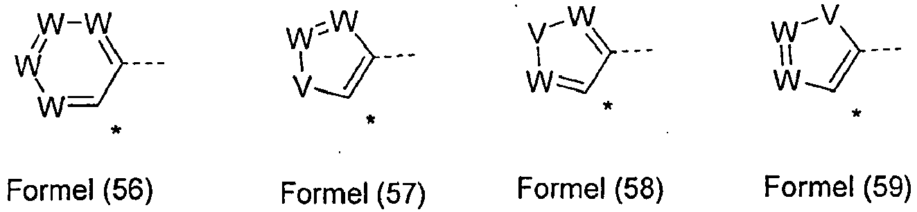
Dabei können die oben genannten bevorzugten Gruppen Ar1, Ar2 und Ar3 beliebig miteinander kombiniert werden.In this case, the above-mentioned preferred groups Ar 1 , Ar 2 and Ar 3 can be combined with each other as desired.
In einer weiteren bevorzugten Ausführungsform der Erfindung steht mindestens eine Gruppe E für eine Einfachbindung.In a further preferred embodiment of the invention, at least one group E is a single bond.
In einer bevorzugten Ausführungsform der Erfindung treten die oben genannten Bevorzugungen gleichzeitig auf. Besonders bevorzugt sind daher Verbindungen gemäß Formel (45) bzw. (46), für die gilt:
- Ar1
- ist ausgewählt aus den Gruppen der oben genannten Formeln (47), (48), (49) oder (50);
- Ar2
- ist ausgewählt aus den Gruppen der oben genannten Formeln (53), (54) oder (55);
- Ar3
- ist ausgewählt aus den Gruppen der oben genannten Formeln (56), (57), (58) oder (59).
- Ar 1
- is selected from the groups of the above formulas (47), (48), (49) or (50);
- Ar 2
- is selected from the groups of the above formulas (53), (54) or (55);
- Ar 3
- is selected from the groups of the above-mentioned formulas (56), (57), (58) or (59).
Besonders bevorzugt stehen mindestens zwei der Gruppen Ar1, Ar2 und Ar3 für eine 6-Ring-Aryl- oder eine 6-Ring-Heteroarylgruppe. Besonders bevorzugt steht also Ar1 für eine Gruppe der Formel (47) und gleichzeitig steht Ar2 für eine Gruppe der Formel (53), oder Ar1 steht für eine Gruppe der Formel (47) und gleichzeitig steht Ar3 für eine Gruppe der Formel (56), oder Ar2 steht für eine Gruppe der Formel (53) und gleichzeitig steht Ar3 für eine Gruppe der Formel (59).Particularly preferably, at least two of the groups Ar 1 , Ar 2 and Ar 3 are a 6-membered aryl or a 6-membered heteroaryl group. Thus Ar 1 is particularly preferably a group of the formula (47) and at the same time Ar 2 is a group of the formula (53) or Ar 1 is a group of the formula (47) and at the same time Ar 3 is a group of the formula (56), or Ar 2 represents a group of the formula (53) and at the same time Ar 3 represents a group of the formula (59).
Besonders bevorzugte Ausführungsformen der Formel (45) sind daher die Verbindungen der folgenden Formeln (60) bis (69),


Es ist weiterhin bevorzugt, wenn W für CR oder N steht und nicht für eine Gruppe der Formel (51) oder (52). In einer bevorzugten Ausführungsform der Verbindungen gemäß Formel (60) bis (69) steht pro Cyclus insgesamt maximal ein Symbol W für N, und die verbleibenden Symbole W stehen für CR. In einer besonders bevorzugten Ausführungsform der Erfindung stehen alle Symbole W für CR. Besonders bevorzugt sind daher die Verbindungen gemäß den folgenden Formeln (60a) bis (69a),


Ganz besonders bevorzugt sind die Strukturen der Formeln (60b) bis (69b),


Ganz besonders bevorzugt sind die Verbindungen der Formel (60) bzw. (60a) bzw. (60b).Very particular preference is given to the compounds of the formula (60) or (60a) or (60b).
Die verbrückende Gruppe L in den Verbindungen der Formeln (46a) ist bevorzugt ausgewählt aus einer Einfachbindung oder einem aromatischen oder heteroaromatischen Ringsystem mit 5 bis 30 aromatischen Ringatomen, welches durch einen oder mehrere Reste R substituiert sein kann. Dabei enthalten die aromatischen bzw. heteroaromatischen Ringsysteme bevorzugt keine kondensierten Aryl- bzw. Heteroarylgruppen, in denen mehr als zwei aromatische Sechsringe direkt aneinander ankondensiert sind. Besonders bevorzugt enthalten sie überhaupt keine Aryl- bzw. Heteroarylgruppen, in denen aromatische Sechsringe direkt aneinander ankondensiert sind.The bridging group L in the compounds of the formula (46a) is preferably selected from a single bond or an aromatic or heteroaromatic ring system having 5 to 30 aromatic ring atoms, which may be substituted by one or more radicals R. The aromatic or heteroaromatic ring systems preferably contain no condensed aryl or heteroaryl groups in which more than two aromatic six-membered rings are directly fused to one another. With particular preference, they contain no aryl or heteroaryl groups at all, in which aromatic six-membered rings are directly fused to one another.
In einer weiteren bevorzugten Ausführungsform der Erfindung ist der Index m in Verbindungen der Formel (46) = 2 oder 3, insbesondere gleich 2.In a further preferred embodiment of the invention, the index m in compounds of the formula (46) = 2 or 3, in particular equal to 2.
In einer bevorzugten Ausführungsform der Erfindung ist R in den oben genannten Formeln gleich oder verschieden bei jedem Auftreten ausgewählt aus der Gruppe bestehend aus H, D, F, Cl, Br, CN, N(Ar)2, C(=O)Ar, einer geradkettigen Alkyl- oder Alkoxygruppe mit 1 bis 10 C-Atomen oder einer verzweigten oder cyclischen Alkyl- oder Alkoxygruppe mit 3 bis 10 C-Atomen oder einer Alkenylgruppe mit 2 bis 10 C-Atomen, die jeweils mit einem oder mehreren Resten R1 substituiert sein kann, wobei eine oder mehrere nicht-benachbarte CH2-Gruppen durch O ersetzt sein können und wobei ein oder mehrere H-Atome durch D oder F ersetzt sein können, einem aromatischen oder heteroaromatischen Ringsystem mit 5 bis 30 aromatischen Ringatomen, das jeweils mit einem oder mehreren Resten R1 substituiert sein kann, einer Aryloxy- oder Heteroaryloxygruppe mit 5 bis 30 aromatischen Ringatomen, die mit einem oder mehreren Resten R1 substituiert sein kann, oder einer Kombination dieser Systeme.In a preferred embodiment of the invention, R in the abovementioned formulas is the same or different at each occurrence selected from the group consisting of H, D, F, Cl, Br, CN, N (Ar) 2 , C (= O) Ar, a straight-chain alkyl or alkoxy group having 1 to 10 C atoms or a branched or cyclic alkyl or alkoxy group having 3 to 10 C atoms or an alkenyl group having 2 to 10 C atoms, each substituted by one or more radicals R 1 may be replaced, wherein one or more non-adjacent CH 2 groups may be replaced by O and wherein one or more H atoms may be replaced by D or F, an aromatic or heteroaromatic ring system having 5 to 30 aromatic ring atoms, each with one or more radicals R 1 may be substituted, an aryloxy or heteroaryloxy group having 5 to 30 aromatic ring atoms which may be substituted by one or more radicals R 1 , or a combination of these systems.
In einer besonders bevorzugten Ausführungsform der Erfindung ist R in den oben genannten Formeln gleich oder verschieden bei jedem Auftreten ausgewählt aus der Gruppe bestehend aus H, D, F, Cl, Br, CN, einer geradkettigen Alkylgruppe mit 1 bis 10 C-Atomen oder einer verzweigten oder cyclischen Alkylgruppe mit 3 bis 10 C-Atomen, die jeweils mit einem oder mehreren Resten R1 substituiert sein kann, wobei ein oder mehrere H-Atome durch D oder F ersetzt sein können, einem aromatischen oder heteroaromatischen Ringsystem mit 5 bis 18 aromatischen Ringatomen, das jeweils mit einem oder mehreren Resten R1 substituiert sein kann, oder einer Kombination dieser Systeme.In a particularly preferred embodiment of the invention, R in the abovementioned formulas is the same or different at each occurrence selected from the group consisting of H, D, F, Cl, Br, CN, a straight-chain alkyl group having 1 to 10 C atoms or a a branched or cyclic alkyl group having 3 to 10 carbon atoms, each of which may be substituted by one or more R 1 radicals, wherein one or more H atoms may be replaced by D or F, an aromatic or heteroaromatic ring system having 5 to 18 aromatic Ring atoms, which may each be substituted by one or more radicals R 1 , or a combination of these systems.
Dabei enthalten die Reste R, wenn diese aromatische oder heteroaromatischen Ringsysteme enthalten, bevorzugt keine kondensierten Aryl- bzw. Heteroarylgruppen, in denen mehr als zwei aromatische Sechsringe direkt aneinander ankondensiert sind. Besonders bevorzugt enthalten sie überhaupt keine Aryl- bzw. Heteroarylgruppen, in denen aromatische Sechsringe direkt aneinander ankondensiert sind. Insbesondere bevorzugt sind hier Phenyl, Biphenyl, Terphenyl, Quaterphenyl, Carbazol, Dibenzothiophen, Dibenzofuran, Indenocarbazol, Indolocarbazol, Triazin oder Pyrimidin, welches jeweils auch durch einen oder mehrere Reste R1 substituiert sein kann.The radicals R, when they contain aromatic or heteroaromatic ring systems, preferably contain no fused aryl or heteroaryl groups in which more than two aromatic six-membered rings are directly fused to one another. With particular preference, they contain no aryl or heteroaryl groups at all, in which aromatic six-membered rings are directly fused to one another. Particular preference is given here to phenyl, biphenyl, terphenyl, quaterphenyl, carbazole, dibenzothiophene, dibenzofuran, indenocarbazole, indolocarbazole, triazine or pyrimidine, which in each case may also be substituted by one or more radicals R 1 .
Dabei haben für Verbindungen, die durch Vakuumverdampfung verarbeitet werden, die Alkylgruppen bevorzugt nicht mehr als fünf C-Atome, besonders bevorzugt nicht mehr als 4 C-Atome, ganz besonders bevorzugt nicht mehr als 1 C-Atom. Für Verbindungen, die aus Lösung verarbeitet werden, eignen sich auch Verbindungen, die mit Alkylgruppen mit bis zu 10 C-Atomen substituiert sind oder die mit Oligoarylengruppen, beispielsweise ortho-, meta-, para- oder verzweigten Terphenylgruppen, substituiert sind.In this case, for compounds which are processed by vacuum evaporation, the alkyl groups preferably have not more than five carbon atoms, more preferably not more than 4 carbon atoms, most preferably not more than 1 carbon atom. For compounds which are processed from solution, compounds which are substituted by alkyl groups having up to 10 carbon atoms or are substituted by oligoarylene groups, for example ortho, meta, para or branched terphenyl groups, are also suitable.
Die Verbindungen der Formeln (45) und (46) sind prinzipiell bekannt. Die Synthese dieser Verbindungen kann gemäß den in der
Beispiele für bevorzugte Verbindungen gemäß den oben aufgeführten Ausführungsformen sind die in der folgenden Tabelle aufgeführten Verbindungen.


Weiterhin eignen sich aromatische Ketone oder aromatische Phosphinoxide als Elektronentransportmaterial in der erfindungsgemäßen Elektronentransportschicht. Unter einem aromatischen Keton im Sinne dieser Anmeldung wird eine Carbonylgruppe verstanden, an die zwei aromatische oder heteroaromatische Gruppen bzw. aromatische oder heteroaromatische Ringsysteme direkt gebunden sind. Unter einem aromatischen Phosphinoxid im Sinne dieser Anmeldung wird eine P=O Gruppe verstanden, an die drei aromatische oder heteroaromatische Gruppen bzw. aromatische oder heteroaromatische Ringsysteme direkt gebunden sindFurthermore, aromatic ketones or aromatic phosphine oxides are suitable as electron transport material in the electron transport layer according to the invention. For the purposes of this application, an aromatic ketone is understood as meaning a carbonyl group to which two aromatic or heteroaromatic groups or aromatic or heteroaromatic ring systems are directly bonded. In the context of this application, an aromatic phosphine oxide is understood as meaning a P =O group to which three aromatic or heteroaromatic groups or aromatic or heteroaromatic ring systems are directly bonded
Wenn das Elektronentransportmaterial in der erfindungsgemäßen Elektronentransportschicht ein aromatisches Keton oder ein aromatisches Phosphinoxid ist, dann ist diese Verbindung bevorzugt ausgewählt aus den Verbindungen der folgenden Formeln (70) bzw. (71),

- Ar4
- ist bei jedem Auftreten gleich oder verschieden ein aromatisches oder heteroaromatisches Ringsystem mit 5 bis 80 aromatischen Ringatomen, bevorzugt bis 60 aromatischen Ringatomen, welches jeweils mit einer oder mehreren Gruppen R substituiert sein kann.
- Ar 4
- is identical or different at each occurrence an aromatic or heteroaromatic ring system having 5 to 80 aromatic ring atoms, preferably up to 60 aromatic ring atoms, which may be substituted in each case with one or more groups R.
Geeignete Verbindungen gemäß Formel (70) und (71) sind insbesondere die in
Aus der Definition der Verbindung gemäß Formel (70) und (70) geht hervor, dass diese nicht nur eine Carbonylgruppe bzw. Phosphinoxidgruppe enthalten muss, sondern auch mehrere dieser Gruppen enthalten kann.From the definition of the compound according to formulas (70) and (70), it is clear that not only does it have to contain one carbonyl group or phosphine oxide group, but it can also contain several of these groups.
Bevorzugt ist die Gruppe Ar4 in Verbindungen gemäß Formel (70) bzw. (71) ein aromatisches Ringsystem mit 6 bis 40 aromatischen Ringatomen, d. h. sie enthält keine Heteroarylgruppen. Wie oben definiert, muss das aromatische Ringsystem nicht notwendigerweise nur aromatische Gruppen aufweisen, sondern es können auch zwei Arylgruppen durch eine nicht-aromatische Gruppe, beispielsweise durch eine weitere Carbonylgruppe bzw. Phosphinoxidgruppe unterbrochen sein.The group Ar 4 in compounds of the formula (70) or (71) is preferably an aromatic ring system having 6 to 40 aromatic ring atoms, ie it contains no heteroaryl groups. As defined above, the aromatic ring system need not necessarily have only aromatic groups, but also two aryl groups may be interrupted by a non-aromatic group, for example by another carbonyl group or phosphine oxide group.
In einer weiteren bevorzugten Ausführungsform der Erfindung weist die Gruppe Ar4 nicht mehr als zwei kondensierte Ringe auf. Sie ist also bevorzugt nur aus Phenyl- und/oder Naphthylgruppen, besonders bevorzugt nur aus Phenylgruppen, aufgebaut, enthält aber keine größeren kondensierten Aromaten, wie beispielsweise Anthracen.In a further preferred embodiment of the invention, the group Ar 4 has no more than two condensed rings. It is therefore preferably composed only of phenyl and / or naphthyl groups, particularly preferably only of phenyl groups, but does not contain any larger condensed aromatics, such as, for example, anthracene.
Bevorzugte Gruppen Ar4, die an die Carbonylgruppe gebunden sind, sind Phenyl, 2-, 3- oder 4-Tolyl, 3- oder 4-o-Xylyl, 2- oder 4-m-Xylyl, 2-p-Xylyl, o-, m- oder p-tert-Butylphenyl, o-, m- oder p-Fluorphenyl, Benzophenon, 1-, 2- oder 3-Phenylmethanon, 2-, 3- oder 4-Biphenyl, 2-, 3- oder 4-o-Terphenyl, 2-, 3- oder 4-m-Terphenyl, 2-, 3- oder 4-p-Terphenyl, 2'-p-Terphenyl, 2'-, 4'- oder 5'-m-Terphenyl, 3'- oder 4'-o-Terphenyl, p-, m,p-, o,p-, m,m-, o,m- oder o,o-Quaterphenyl, Quinquephenyl, Sexiphenyl, 1-, 2-, 3- oder 4-Fluorenyl, 2-, 3- oder 4-Spiro-9,9'-bifluorenyl, 1-, 2-, 3- oder 4-(9,10-Dihydro)phenanthrenyl, 1- oder 2-Naphthyl, 2-, 3-, 4-, 5-, 6-, 7-oder 8-Chinolinyl, 1-, 3-, 4-, 5-, 6-, 7- oder 8-iso-Chinolinyl, 1- oder 2-(4-Methylnaphthyl), 1- oder 2-(4-Phenylnaphthyl), 1- oder 2-(4-Naphthyl-naphthyl), 1-, 2- oder 3-(4-naphthyl-phenyl), 2-, 3- oder 4-Pyridyl, 2-, 4-oder 5-Pyrimidinyl, 2- oder 3-Pyrazinyl, 3- oder 4-Pyridanzinyl, 2-(1,3,5-Triazin)yl-, 2-, 3- oder 4-(Phenylpyridyl), 3-, 4-, 5- oder 6-(2,2'-Bipyridyl), 2-, 4-, 5- oder 6-(3,3'-Bipyridyl), 2- oder 3-(4,4'-Bipyridyl) und Kombinationen eines oder mehrerer dieser Reste.Preferred groups Ar 4 which are bonded to the carbonyl group are phenyl, 2-, 3- or 4-tolyl, 3- or 4-o-xylyl, 2- or 4-m-xylyl, 2-p-xylyl, o -, m- or p-tert-butylphenyl, o-, m- or p-fluorophenyl, benzophenone, 1-, 2- or 3-phenylmethanone, 2-, 3- or 4-biphenyl, 2-, 3- or 4 -o-terphenyl, 2-, 3- or 4-m-terphenyl, 2-, 3- or 4-p-terphenyl, 2'-p-terphenyl, 2'-, 4'- or 5'-m-terphenyl , 3'- or 4'-o-terphenyl, p-, m, p-, o, p-, m, m-, o, m- or o, o-quaterphenyl, quinquephenyl, sexiphenyl, 1-, 2-, 3- or 4-fluorenyl, 2-, 3- or 4-spiro-9, 9'-bifluorenyl, 1-, 2-, 3- or 4- (9,10-dihydro) -phenanthrenyl, 1- or 2-naphthyl, 2-, 3-, 4-, 5-, 6-, 7-or 8-quinolinyl, 1-, 3-, 4-, 5-, 6-, 7- or 8-iso-quinolinyl, 1- or 2- (4-methylnaphthyl), 1- or 2- (4-phenylnaphthyl), 1- or 2- (4-naphthyl-naphthyl), 1-, 2- or 3- (4-naphthyl-phenyl), 2-, 3- or 4-pyridyl, 2-, 4- or 5-pyrimidinyl, 2 or 3-pyrazinyl, 3- or 4-pyridanzinyl, 2- (1,3,5-triazine) yl, 2-, 3- or 4- (phenylpyridyl), 3-, 4-, 5- or 6- (2,2'-bipyridyl), 2-, 4-, 5- or 6- (3,3'-bipyridyl), 2- or 3- (4,4'-bipyridyl) and combinations of one or more of these radicals.
Die Gruppen Ar4 können durch einen oder mehrere Reste R substituiert sein. Diese Reste R1 sind bevorzugt gleich oder verschieden bei jedem Auftreten gewählt aus der Gruppe bestehend aus H, D, F, C(=O)Ar, P(=O)(Ar)2, S(=O)Ar, S(=O)2Ar, einer geradkettigen Alkylgruppe mit 1 bis 4 C-Atomen oder einer verzweigten oder cyclischen Alkylgruppe mit 3 bis 5 C-Atomen, die jeweils mit einem oder mehreren Resten R1 substituiert sein kann, wobei ein oder mehrere H-Atome durch F ersetzt sein können, oder einem aromatischen Ringsystem mit 6 bis 24 aromatischen Ringatomen, das durch einen oder mehrere Reste R1 substituiert sein kann, oder eine Kombination dieser Systeme; dabei können zwei oder mehrere benachbarte Substituenten R auch miteinander ein mono- oder polycyclisches, aliphatisches oder aromatisches Ringsystem bilden. Wenn die organische Elektrolumineszenzvorrichtung aus Lösung aufgebracht wird, sind auch geradkettige, verzweigte oder cyclische Alkylgruppen mit bis zu 10 C-Atomen als Substituenten R bevorzugt. Die Reste R sind besonders bevorzugt gleich oder verschieden bei jedem Auftreten gewählt aus der Gruppe bestehend aus H, C(=O)Ar oder einem aromatischen Ringsystem mit 6 bis 24 aromatischen Ringatomen, das durch einen oder mehrere Reste R1 substituiert sein kann, bevorzugt aber unsubstituiert ist.The groups Ar 4 may be substituted by one or more radicals R. These radicals R 1 are preferably identical or different in each occurrence selected from the group consisting of H, D, F, C (OO) Ar, P (OO) (Ar) 2 , S (OO) Ar, S ( = O) 2 Ar, a straight-chain alkyl group having 1 to 4 C atoms or a branched or cyclic alkyl group having 3 to 5 C atoms, each of which may be substituted by one or more R 1 radicals, one or more H atoms be replaced by F, or an aromatic ring system having 6 to 24 aromatic ring atoms, which may be substituted by one or more radicals R 1 , or a combination of these systems; two or more adjacent substituents R may also together form a mono- or polycyclic, aliphatic or aromatic ring system. When the organic electroluminescent device is applied from solution, straight-chain, branched or cyclic alkyl groups having up to 10 C atoms are also preferred as substituents R. The radicals R are particularly preferably identical or different at each occurrence selected from the group consisting of H, C (= O) Ar or an aromatic ring system having 6 to 24 aromatic ring atoms, which may be substituted by one or more radicals R 1 , preferably but is unsubstituted.
In nochmals einer bevorzugten Ausführungsform der Erfindung ist die Gruppe Ar gleich oder verschieden bei jedem Auftreten ein aromatisches Ringsystem mit 6 bis 24 aromatischen Ringatomen, das mit einem oder mehreren Resten R1 substituiert sein kann. Besonders bevorzugt ist Ar gleich oder verschieden bei jedem Auftreten ein aromatisches Ringsystem mit 6 bis 12 aromatischen Ringatomen.In yet a further preferred embodiment of the invention, the group Ar is the same or different at each occurrence, an aromatic ring system having 6 to 24 aromatic ring atoms, which may be substituted by one or more radicals R 1 . Particularly preferred is Ar identical or different at each occurrence, an aromatic ring system having 6 to 12 aromatic ring atoms.
Besonders bevorzugt sind Benzophenon-Derivate, die jeweils an den 3,5,3',5'-Positionen durch ein aromatisches oder heteroaromatisches Ringsystem mit 5 bis 30 aromatischen Ringatomen substituiert sind, welche wiederum durch einen oder mehrere Reste R gemäß der obigen Definition substituiert sein kann. Weiterhin bevorzugt sind Ketone, welche mit mindestens einer Spirobifluorengruppe substituiert sind.Particularly preferred are benzophenone derivatives each substituted at the 3,5,3 ', 5' positions by an aromatic or heteroaromatic ring system having from 5 to 30 aromatic ring atoms which in turn are substituted by one or more Rs as defined above can be. Preference is furthermore given to ketones which are substituted by at least one spirobifluorene group.
Bevorzugte aromatische Ketone und Phosphinoxide sind daher die Verbindungen der folgenden Formel (72) bis (75),


- T
- ist gleich oder verschieden bei jedem Auftreten C oder P(Ar4);
- n
- ist gleich oder verschieden bei jedem Auftreten 0 oder 1.
- T
- is the same or different at each occurrence, C or P (Ar 4 );
- n
- is the same or different at every occurrence 0 or 1.
Bevorzugt steht Ar4 in der oben genannten Formel (72) und (75) für ein aromatisches oder heteroaromatisches Ringsystem mit 5 bis 30 aromatischen Ringatomen, welches mit einem oder mehreren Resten R1 substituiert sein kann. Besonders bevorzugt sind die oben genannten Gruppen Ar.Ar 4 in the abovementioned formula (72) and (75) preferably represents an aromatic or heteroaromatic ring system having 5 to 30 aromatic ring atoms which is substituted by one or more radicals R 1 can be. Particularly preferred are the abovementioned groups Ar.
Beispiele für geeignete Verbindungen gemäß Formel (70) und (71) sind die in der folgenden Tabelle abgebildeten Verbindungen.


Geeignete Metallkomplexe, die als Elektronentransportmaterial in der erfindungsgemäßen Elektronentransportschicht eingesetzt werden können, sind Be-, Zn- bzw. Al-Komplexe, sofern das LUMO dieser Verbindungen ≤ -2.55 eV beträgt.Suitable metal complexes which are used as electron transport material in the electron transport layer according to the invention are Be, Zn or Al complexes, provided the LUMO of these compounds is ≤ -2.55 eV.
Beispiele für geeignete Metallkomplexe sind die in der folgenden Tabelle abgebildeten Verbindungen.

In einer bevorzugten Ausführungsform der Erfindung handelt es sich bei den Elektronentransportmaterialien mit einem LUMO ≤ -2.55 eV in der erfindungsgemäßen Elektronentransportschichten jedoch um rein organische Materialien, also um Materialien, die kein Metall enthalten.In a preferred embodiment of the invention, however, the electron transport materials having a LUMO ≦ -2.55 eV in the electron transport layers according to the invention are purely organic materials, ie materials which contain no metal.
Geeignete Azaphosphole, die als elektronenleitendes Matrixmaterial in der erfindungsgemäßen organischen Elektrolumineszenzvorrichtung eingesetzt werden können, sind solche Verbindungen, wie sie in
Geeignete Azaborole, die als elektronenleitendes Matrixmaterial in der erfindungsgemäßen organischen Elektrolumineszenzvorrichtung eingesetzt werden können, sind Azaborolderivate, welche mit mindestens einem elektronenleitenden Substituenten substituiert sind, sofern das LUMO dieser Verbindungen ≤ -2.55 eV beträgt. Solche Verbindungen sind in der noch nicht offen gelegten Anmeldung
Weiterhin geeignet sind Benzimidazolderivate. Damit diese ein LUMO ≤ -2.55 eV aufweisen, ist es bevorzugt, dass an das Benzimidazol direkt oder über eine gegebenenfalls substituierte bivalente aromatische oder heteroaromatische Gruppe eine kondensierte Arylgruppe gebunden ist, insbesondere ein Anthacen, Benzanthracen oder Pyren. Dabei kann sowohl das Benzimidazol wie auch die kondensierte Arylgruppe optional substituiert sein. Geeignete Substituenten sind für die Benzimidazolderivate die oben beschriebenen Reste R.Also suitable are benzimidazole derivatives. In order for them to have a LUMO ≤ -2.55 eV, it is preferred that a fused aryl group is attached to the benzimidazole directly or via an optionally substituted bivalent aromatic or heteroaromatic group, in particular an anthracene, benzanthracene or pyrene. In this case, both the benzimidazole and the condensed aryl group may be optionally substituted. Suitable substituents for the benzimidazole derivatives are the radicals R. described above.
Im Folgenden wird die organische Elektrolumineszenzvorrichtung näher beschrieben.In the following, the organic electroluminescent device will be described in detail.
Die organische Elektrolumineszenzvorrichtung enthält Kathode, Anode, emittierende Schicht und auf Kathodenseite daran angrenzend mindestens eine Elektronentransportschicht. Außer diesen Schichten kann sie noch weitere Schichten enthalten, beispielsweise jeweils eine oder mehrere Lochinjektionsschichten, Lochtransportschichten, weitere Elektronentransportschichten, Elektroneninjektionsschichten, Exzitonenblockierschichten, Elektronenblockierschichten und/oder Ladungserzeugungsschichten (Charge-Generation Layers). Es sei aber darauf hingewiesen, dass nicht notwendigerweise jede dieser Schichten vorhanden sein muss.The organic electroluminescent device includes cathode, anode, emissive layer and, on the cathode side thereof, at least one electron transport layer adjacent thereto. In addition to these layers, they may also contain further layers, for example one or more hole injection layers, hole transport layers, further electron transport layers, electron injection layers, exciton blocking layers, electron blocking layers and / or charge generation layers (charge generation layers). It should be noted, however, that not necessarily each of these layers must be present.
In den weiteren Schichten der erfindungsgemäßen organischen Elektrolumineszenzvorrichtung, insbesondere in den Lochinjektions- und -transportschichten und in den Elektroneninjektions- und -transportschichten, können alle Materialien verwendet werden, wie sie üblicherweise gemäß dem Stand der Technik eingesetzt werden. Dabein können die Lochtransportschichten auch p-dotiert bzw. die Elektronentransportschichten auch n-dotiert sein. Dabei wird unter einer p-dotierten Schicht eine Schicht verstanden, in der freie Löcher erzeugt wurden und deren Leitfähigkeit dadurch erhöht ist. Eine umfassende Diskussion von dotierten Transportschichten in OLEDs findet sich in
Der Fachmann kann daher ohne erfinderisches Zutun alle für organische Elektrolumineszenzvorrichtungen bekannten Materialien in Kombination mit der erfindungsgemäßen emittierenden Schicht einsetzen.The person skilled in the art can therefore use all materials known for organic electroluminescent devices in combination with the emitting layer according to the invention without inventive step.
Insbesondere kann es bevorzugt sein, wenn zwischen der erfindungsgemäßen Elektronentransportschicht und der Kathode weitere Elektronentransportschichten und/oder Elektroneninjektionsschichten vorliegen. In einer bevorzugten Ausführungsform der Erfindung enthält die weitere Elektronentransportschicht und/oder Elektroneninjektionsschicht eine Lithiumverbindung, beispielsweise LiQ (Lithiumchinolinat). Weitere geeignete Lithiumverbindungen können der
Weiterhin kann es bevorzugt sein, wenn die Elektronentransportschicht, die an die Kathode oder, falls vorhanden, an die Elektroneninjektionsschicht angrenzt, eine Mischung enthält aus einem Elektronentransportmaterial mit einem LUMO ≤ -2.55 eV und einer Lithiumverbindung, insbesondere Lithiumchinolinat oder einem Lithiumchinolinatderivat.Furthermore, it may be preferable if the electron transport layer adjacent to the cathode or, if present, the electron injection layer contains a mixture of an electron transport material having a LUMO ≦ -2.55 eV and a lithium compound, in particular lithium quinolinate or a lithium quinolinate derivative.
Als Kathode der erfindungsgemäßen Elektrolumineszenzvorrichtung sind Metalle mit geringer Austrittsarbeit, Metalllegierungen oder mehrlagige Strukturen aus verschiedenen Metallen bevorzugt, wie beispielsweise Erdalkalimetalle, Alkalimetalte, Hauptgruppenmetalle oder Lanthanoide (z. B. Ca, Ba, Mg, Al, In, Mg, Yb, Sm, etc.). Bei mehrlagigen Strukturen können auch zusätzlich zu den genannten Metallen weitere Metalle verwendet werden, die eine relativ hohe Austrittsarbeit aufweisen, wie z. B. Ag, wobei dann in der Regel Kombinationen der Metalle, wie beispielsweise Mg/Ag, Ca/Ag oder Ba/Ag verwendet werden. Ebenso bevorzugt sind Metalllegierungen, insbesondere Legierungen aus einem Alkalimetall oder Erdalkalimetall und Silber, besonders bevorzugt eine Legierung aus Mg und Ag. Es kann auch bevorzugt sein, zwischen einer metallischen Kathode und dem organischen Halbleiter eine dünne Zwischenschicht eines Materials mit einer hohen Dielektrizitätskonstante einzubringen. Hierfür kommen beispielsweise Alkalimetall- oder Erdalkalimetallfluoride, aber auch die entsprechenden Oxide oder Carbonate in Frage (z. B. LiF, Li2O, CsF, Cs2CO3, BaF2, MgO, NaF, etc.). Ebenso kommen organische Alkali- oder Erdalkalikomplexe in Frage, wie z. B. Lithiumchinolinat (LiQ). Die Schichtdicke dieser Schicht, die als Elektroneninjektionsschicht anzusehen ist, beträgt bevorzugt zwischen 0.5 und 5 nm.Preferred as the cathode of the electroluminescent device according to the invention are low work function metals, metal alloys or multilayer structures of different metals, such as alkaline earth metals, alkali metals, main group metals or lanthanides (eg Ca, Ba, Mg, Al, In, Mg, Yb, Sm, Etc.). In multilayer structures, it is also possible, in addition to the metals mentioned, to use further metals which have a relatively high work function, such as, for example, B. Ag, which then usually combinations of metals, such as Mg / Ag, Ca / Ag or Ba / Ag are used. Likewise preferred are metal alloys, in particular alloys of an alkali metal or alkaline earth metal and silver, particularly preferably an alloy of Mg and Ag. It may also be preferred to introduce between a metallic cathode and the organic semiconductor a thin intermediate layer of a material with a high dielectric constant. Suitable examples of these are alkali metal or alkaline earth metal fluorides, but also the corresponding oxides or carbonates (eg LiF, Li 2 O, CsF, Cs 2 CO 3 , BaF 2 , MgO, NaF, etc.). Likewise, organic alkali or alkaline earth metal complexes in question, such as. For example, lithium quinolinate (LiQ). The layer thickness of this layer, which is to be regarded as an electron injection layer, is preferably between 0.5 and 5 nm.
Als Anode der erfindungsgemäßen Elektrolumineszenzvorrichtung sind Materialien mit hoher Austrittsarbeit bevorzugt. Bevorzugt weist die Anode eine Austrittsarbeit größer 4.5 eV vs. Vakuum auf. Hierfür sind einerseits Metalle mit hohem Redoxpotential geeignet, wie beispielsweise Ag, Pt oder Au. Es können andererseits auch Metall/Metalloxid-Elektroden (z. B. Al/Ni/NiOx, Al/PtOx) bevorzugt sein. Dabei muss mindestens eine der Elektroden transparent oder teiltransparent sein, um die Auskopplung von Licht zu ermöglichen. Bevorzugte transparente oder teiltransparente Anodenmaterialien sind leitfähige gemischte Metalloxide. Besonders bevorzugt sind Indium-Zinn-Oxid (ITO) oder Indium-Zink-Oxid (IZO). Bevorzugt sind weiterhin leitfähige, dotierte organische Materialien, insbesondere leitfähige dotierte Polymere.As the anode of the electroluminescent device according to the invention, materials having a high work function are preferred. Preferably, the anode has a work function greater than 4.5 eV. Vacuum up. On the one hand, metals with a high redox potential, such as Ag, Pt or Au, are suitable for this purpose. On the other hand, metal / metal oxide electrodes (for example Al / Ni / NiO x , Al / PtO x ) may also be preferred. At least one of the electrodes must be transparent or partially transparent in order to enable the extraction of light. Preferred transparent or partially transparent Anode materials are conductive mixed metal oxides. Particularly preferred are indium tin oxide (ITO) or indium zinc oxide (IZO). Preference is furthermore given to conductive, doped organic materials, in particular conductive doped polymers.
Die Vorrichtung wird entsprechend (je nach Anwendung) strukturiert, kontaktiert und schließlich hermetisch versiegelt, da sich die Lebensdauer derartiger Vorrichtungen bei Anwesenheit von Wasser und/oder Luft drastisch verkürzt.The device is structured accordingly (depending on the application), contacted and finally hermetically sealed because the life of such devices drastically shortened in the presence of water and / or air.
Weiterhin bevorzugt ist eine organische Elektrolumineszenzvorrichtung, dadurch gekennzeichnet, dass eine oder mehrere Schichten mit einem Sublimationsverfahren beschichtet werden. Dabei werden die Materialien in Vakuum-Sublimationsanlagen bei einem Anfangsdruck kleiner 10-5 mbar, bevorzugt kleiner 10-6 mbar aufgedampft. Es ist aber auch möglich, dass der Anfangsdruck noch geringer ist, beispielsweise kleiner 10-7 mbar.Further preferred is an organic electroluminescent device, characterized in that one or more layers are coated with a sublimation process. The materials are vapor-deposited in vacuum sublimation systems at an initial pressure of less than 10 -5 mbar, preferably less than 10 -6 mbar. But it is also possible that the initial pressure is even lower, for example less than 10 -7 mbar.
Bevorzugt ist ebenfalls eine organische Elektrolumineszenzvorrichtung, dadurch gekennzeichnet, dass eine oder mehrere Schichten mit dem OVPD (Organic Vapour Phase Deposition) Verfahren oder mit Hilfe einer Trägergassublimation beschichtet werden. Dabei werden die Materialien bei einem Druck zwischen 10-5 mbar und 1 bar aufgebracht. Ein Spezialfall dieses Verfahrens ist das OVJP (Organic Vapour Jet Printing) Verfahren, bei dem die Materialien direkt durch eine Düse aufgebracht und so strukturiert werden (z.
Weiterhin bevorzugt ist eine organische Elektrolumineszenzvorrichtung, dadurch gekennzeichnet, dass eine oder mehrere Schichten aus Lösung, wie z. B. durch Spincoating, oder mit einem beliebigen Druckverfahren, wie z. B. Siebdruck, Flexodruck, Offsetdruck, LITI (Light Induced Thermal Imaging, Thermotransferdruck), Ink-Jet Druck (Tintenstrahldruck) oder Nozzle Printing, hergestellt werden. Hierfür sind lösliche Verbindungen nötig, welche beispielsweise durch geeignete Substitution erhalten werden. Diese Verfahren eignen sich insbesondere auch für Oligomere, Dendrimere und Polymere.Further preferred is an organic electroluminescent device, characterized in that one or more layers of solution, such. B. by spin coating, or with any printing process, such. As screen printing, flexographic printing, offset printing, LITI (Light Induced Thermal Imaging, thermal transfer printing), ink-jet printing (ink jet printing) or Nozzle Printing, are produced. For this purpose, soluble compounds are necessary, which are obtained for example by suitable substitution become. These methods are particularly suitable for oligomers, dendrimers and polymers.
Diese Verfahren sind dem Fachmann generell bekannt und können von ihm ohne erfinderisches Zutun auf organische Elektrolumineszenzvorrichtungen enthaltend die erfindungsgemäßen Verbindungen angewandt werden.These methods are generally known to the person skilled in the art and can be applied by him without inventive step to organic electroluminescent devices comprising the compounds according to the invention.
Ein weiterer Gegenstand der vorliegenden Erfindung ist daher ein Verfahren zur Herstellung einer erfindungsgemäßen organischen Elektrolumineszenzvorrichtung, dadurch gekennzeichnet, dass mindestens eine Schicht mit einem Sublimationsverfahren aufgebracht wird und/oder dass mindestens eine Schicht mit einem OVPD (Organic Vapour Phase Deposition) Verfahren oder mit Hilfe einer Trägergassublimation aufgebracht wird und/oder dass mindestens eine Schicht aus Lösung, durch Spincoating oder mit einem Druckverfahren aufgebracht wird.Another object of the present invention is therefore a method for producing an organic electroluminescent device according to the invention, characterized in that at least one layer is applied by a sublimation and / or that at least one layer with an OVPD (Organic Vapor Phase Deposition) method or by means of a Carrier gas sublimation is applied and / or that at least one layer of solution, by spin coating or by a printing process is applied.
Die erfindungsgemäßen organischen Elektrolumineszenzvorrichtungen zeichnen sich durch einen oder mehrere der folgenden überraschenden Vorteile gegenüber dem Stand der Technik aus:
- 1. Die erfindungsgemäßen organischen Elektrolumineszenzvorrichtungen weisen eine sehr gute und gegenüber Vorrichtungen gemäß dem Stand der Technik, die ebenfalls TADF zeigen, eine verbesserte Effizienz auf.
- 2. Die erfindungsgemäßen organischen Elektrolumineszenzvorrichtungen weisen eine sehr geringe Spannung auf.
- 3. Die erfindungsgemäßen organischen Elektrolumineszenzvorrichtungen weisen eine sehr gute und gegenüber Vorrichtungen gemäß dem Stand der Technik, die ebenfalls TADF zeigen, eine verbesserte Lebensdauer auf.
- 4. Im Vergleich zu organischen Elektrolumineszenzvorrichtungen gemäß dem Stand der Technik, die Iridium- oder Platinkomplexe als emittierende Verbindungen enthalten, weisen die erfindungsgemäßen Elektrolumineszenzvorrichtungen eine verbesserte Lebensdauer bei erhöhter Temperatur auf.
- 1. The organic electroluminescent devices according to the invention have a very good and compared to devices according to the prior art, which also show TADF, improved efficiency.
- 2. The organic electroluminescent devices according to the invention have a very low voltage.
- 3. The organic electroluminescent devices according to the invention have a very good and compared to devices according to the prior art, which also show TADF, an improved lifetime.
- 4. In comparison to organic electroluminescent devices according to the prior art, the iridium or platinum complexes as containing emitting compounds, the electroluminescent devices according to the invention have an improved lifetime at elevated temperature.
Diese oben genannten Vorteile gehen nicht mit einer Verschlechterung der weiteren elektronischen Eigenschaften einher.These advantages mentioned above are not accompanied by a deterioration of the other electronic properties.
Die Erfindung wird durch die nachfolgenden Beispiele näher erläutert, ohne sie dadurch einschränken zu wollen. Der Fachmann kann aus den Schilderungen die Erfindung im gesamten offenbarten Bereich ausführen und ohne erfinderisches Zutun weitere erfindungsgemäße organische Elektrolumineszenzvorrichtungen herstellen.The invention is explained in more detail by the following examples without wishing to restrict them thereby. The person skilled in the art can, from the descriptions, carry out the invention in the entire disclosed area and produce inventive organic electroluminescent devices without inventive step.
Die HOMO- und LUMO-Energieniveaus sowie die Energie des niedrigsten Triplettzustands T1 bzw. des niedrigsten angeregten Singulettzustands S1 der Materialien werden über quantenchemische Rechnungen bestimmt. Hierzu wird das Programmpaket "Gaussian09W" (Gaussian Inc.) verwendet. Zur Berechnung organischer Substanzen ohne Metalle (in Tabelle 4 mit Methode "org." bezeichnet) wird zuerst eine Geometrieoptimierung mit der Methode "Ground State/Semi-empirical/Default Spin/AM1/Charge 0/Spin Singlet" durchgeführt. Im Anschluss erfolgt auf Grundlage der optimierten Geometrie eine Energierechnung. Hierbei wird die Methode "TD-SFC/DFT/Default Spin/B3PW91" mit dem Basissatz "6-31G(d)" verwendet (Charge 0, Spin Singlet). Für metallhaltige Verbindungen (in Tabelle 4 mit Methode "M-org." bezeichnet) wird die Geometrie über die Methode "Ground State/Hartree-Fock/Default Spin/LanL2MB/Charge 0/Spin Singlet" optimiert. Die Energierechnung erfolgt analog zu den organischen Substanzen, wie oben beschrieben, mit dem Unterschied, dass für das Metallatom der Basissatz "LanL2DZ" und für die Liganden der Basissatz "6-31G(d)" verwendet wird. Aus der Energierechnung erhält man das HOMO-Energieniveau HEh bzw. LUMO-Energieniveau LEh in Hartree-Einheiten. Daraus werden die anhand von Cyclovoltammetriemessungen kalibrierten HOMO- und LUMO-Energieniveaus in Elektronenvolt wie folgt bestimmt: ![]()
![]()
![]()
![]()
Diese Werte sind im Sinne dieser Anmeldung als HOMO- bzw. LUMO-Energieniveaus der Materialien anzusehen.For the purposes of this application, these values are to be regarded as HOMO or LUMO energy levels of the materials.
Der niedrigste Triplettzustand T1 ist definiert als die Energie des Triplettzustands mit der niedrigsten Energie, der sich aus der beschriebenen quantenchemischen Rechnung ergibt.The lowest triplet state T 1 is defined as the energy of the triplet state with the lowest energy, which results from the described quantum chemical calculation.
Der niedrigste angeregte Singulettzustand S1 ist definiert als die Energie des angeregten Singulettzustands mit der niedrigsten Energie, der sich aus der beschriebenen quantenchemischen Rechnung ergibt.The lowest excited singlet state S 1 is defined as the energy of the excited singlet state to the lowest energy, resulting from the described quantum chemical calculation.
In Tabelle 4 sind die HOMO- und LUMO-Energieniveaus sowie S1 und T1 der verschiedenen Materialien angegeben.Table 4 shows the HOMO and LUMO energy levels as well as S 1 and T 1 of the various materials.
Von den in den verschiedenen OLEDs verwendeten Emissionsschichten wird ein 50 nm dicker Film auf ein geeignetes transparentes Substrat, vorzugsweise Quarz, aufgebracht, d. h. die Schicht enthält dieselben Materialien in derselben Konzentration wie in der OLED. Hierbei werden die gleichen Herstellungsbedingungen wie bei der Herstellung der Emissionsschicht für die OLEDs verwendet. Von diesem Film wird ein Absorptionsspektrum im Wellenlängenbereich von 350-500 nm gemessen. Hierzu wird das Reflexionsspektrum R(λ) sowie das Transmissionsspektrum T(λ) der Probe unter einem Einfallswinkel von 6° (also nahezu senkrechter Einfall) bestimmt. Als Absorptionsspektrum im Sinne dieser Anmeldung wird A(λ)=1-R(λ)-T(λ) definiert.Of the emission layers used in the various OLEDs, a 50 nm thick film is applied to a suitable transparent substrate, preferably quartz, i. E. H. the layer contains the same materials in the same concentration as in the OLED. Here, the same manufacturing conditions as in the production of the emission layer for the OLEDs are used. From this film, an absorption spectrum in the wavelength range of 350-500 nm is measured. For this purpose, the reflection spectrum R (λ) and the transmission spectrum T (λ) of the sample is determined at an angle of incidence of 6 ° (ie, almost vertical incidence). For the purpose of this application, the absorption spectrum is defined as A (λ) = 1-R (λ) -T (λ).
Gilt A(λ) ≤ 0.3 im Bereich 350-500nm, so wird die zum Maximum des Absorptionsspektrums gehörige Wellenlänge im Bereich 350-500 nm als λexc definiert. Gilt für irgendeine Wellenlänge A(λ) > 0.3, so wird als λexc die größte Wellenlänge definiert, bei der A(λ) von einem Wert kleiner 0.3 zu einem Wert größer 0.3 oder von einem Wert größer 0.3 zu einem Wert kleiner 0.3 wechselt.If A (λ) ≦ 0.3 is in the range 350-500 nm, then the wavelength belonging to the maximum of the absorption spectrum in the range 350-500 nm is defined as λ exc . If, for any wavelength A (λ)> 0.3, λ exc is the maximum wavelength at which A (λ) changes from a value smaller than 0.3 to a value greater than 0.3 or from a value greater than 0.3 to a value smaller than 0.3.
Zur Bestimmung der PLQE wird ein Messplatz Hamamatsu C9920-02 verwendet. Das Prinzip beruht auf der Anregung der Probe mit Licht definierter Wellenlänge und der Messung der absorbierten und emittierten Strahlung. Die Probe befindet sich während der Messung in einer Ulbrichtkugel ("integrating sphere"). Das Spektrum des Anregungslichts ist in etwa gaußförmig mit einer Halbwertsbreite < 10 nm und Peakwellenlänge λexc wie oben definiert.For the determination of the PLQE a measuring station Hamamatsu C9920-02 is used. The principle is based on the excitation of the sample with light of defined wavelength and the measurement of the absorbed and emitted radiation. The sample is in an integrating sphere during the measurement. The spectrum of the excitation light is defined approximately Gaussian with a half-width of <10 nm and the peak wavelength λ exc above.
Die PLQE wird nach dem für den genannten Messplatz üblichen Auswerteverfahren bestimmt. Es ist strengstens darauf zu achten, dass die Probe zu keinem Zeitpunkt mit Sauerstoff in Berührung kommt, da die PLQE von Materialien mit kleinem energetischen Abstand zwischen S1 und T1 durch Sauerstoff sehr stark reduziert wird (
In Tabelle 2 ist die PLQE für die Emissionsschichten der OLEDs wie oben definiert zusammen mit der verwendeten Anregungswellenlänge angegeben.Table 2 shows the PLQE for the emission layers of the OLEDs as defined above together with the excitation wavelength used.
Zur Bestimmung der Abklingzeit wird eine Probe verwendet, die wie oben unter "Bestimmung der PL-Quanteneffizienz (PLQE)" beschrieben hergestellt wird. Die Probe wird bei einer Temperatur von 295 K durch einen Laserpuls angeregt (Wellenlänge 266 nm, Pulsdauer 1.5 ns, Pulsenergie 200 µJ, Strahldurchmesser 4 mm). Die Probe befindet sich hierbei im Vakuum (<10-5 mbar). Nach der Anregung (definiert als t = 0) wird der zeitliche Verlauf der Intensität der emittierten Photolumineszenz gemessen. Die Photolumineszenz zeigt am Anfang einen steilen Abfall, der auf die prompte Fluoreszenz der TADF-Verbindung zurückzuführen ist. Im weiteren zeitlichen Verlauf ist ein langsamerer Abfall zu beobachten, die verzögerte Fluoreszenz (siehe z.B.
Tabelle 2 zeigt die Werte von ta und td, die für die Emissionsschichten der erfindungsgemäßen OLEDs ermittelt werden.Table 2 shows the values of t a and t d , which are determined for the emission layers of the OLEDs according to the invention.
In den folgenden Beispielen V1 bis E16 (siehe Tabellen 1 und 2) werden die Daten verschiedener OLEDs vorgestellt.In the following examples V1 to E16 (see Tables 1 and 2) the data of different OLEDs are presented.
Glasplättchen, die mit strukturiertem ITO (Indium Zinn Oxid) der Dicke 50 nm beschichtet sind, bilden die Substrate für die OLEDs. Die Substrate werden nass gereinigt (Spülmaschine, Reiniger Merck Extran), anschließend 15 min lang bei 250 °C ausgeheizt und vor der Beschichtung 130s lang mit einem Sauerstoffplasma behandelt. Diese mit Plasma behandelten Glasplättchen bilden die Substrate, auf welche die OLEDs aufgebracht werden. Die Substrate verbleiben vor der Beschichtung im Vakuum. Die Beschichtung beginnt spätestens 10 min nach der Plasmabehandlung.Glass plates coated with structured ITO (Indium Tin Oxide) of thickness 50 nm form the substrates for the OLEDs. The substrates are wet-cleaned (dishwasher, Merck Extran cleaner), then baked at 250 ° C. for 15 minutes and treated with an oxygen plasma for 130 seconds before coating. These plasma-treated glass slides form the substrates to which the OLEDs are applied. The substrates remain in vacuum before coating. The coating begins no later than 10 minutes after the plasma treatment.
Die OLEDs haben prinzipiell folgenden Schichtaufbau: Substrat / optionale Lochinjektionsschicht (HIL) / optionale Lochtransportschicht (HTL) / optionale Zwischenschicht (IL) / Elektronenblockerschicht (EBL) / Emissionsschicht (EML) / optionale Lochblockierschicht (HBL) / Elektronentransportschicht (ETL) / optionale Elektroneninjektionsschicht (EIL) und abschließend eine Kathode. Die Kathode wird durch eine 100 nm dicke Aluminiumschicht gebildet. Der genaue Aufbau der OLEDs ist Tabelle 1 zu entnehmen. Die zur Herstellung der OLEDs benötigten Materialien sind in Tabelle 3 gezeigt.The OLEDs have in principle the following layer structure: Substrate / optional hole injection layer (HIL) / optional hole transport layer (HTL) / optional interlayer (IL) / electron blocker layer (EBL) / emission layer (EML) / optional hole blocking layer (HBL) / electron transport layer (ETL) / optional electron injection layer (EIL) and finally a cathode. The cathode is formed by a 100 nm thick aluminum layer. The exact structure of the OLEDs is shown in Table 1. The materials needed to make the OLEDs are shown in Table 3.
Alle Materialien werden in einer Vakuumkammer thermisch aufgedampft. Dabei besteht die Emissionsschicht immer aus einem Matrixmaterial (Hostmaterial, Wirtsmaterial) und der emittierenden TADF-Verbindung, also dem Material, das einen kleinen energetischen Abstand zwischen S1 und T1 zeigt. Dieses wird dem Matrixmaterial durch Coverdampfung in einem bestimmten Volumenanteil beigemischt. Eine Angabe wie IC1:D1 (95%:5%) bedeutet hierbei, dass das Material IC1 in einem Volumenanteil von 95% und D1 in einem Anteil von 5% in der Schicht vorliegt. Analog kann auch die Elektronentransportschicht aus einer Mischung von zwei Materialien bestehen.All materials are thermally evaporated in a vacuum chamber. In this case, the emission layer always consists of a matrix material (host material, host material) and the emitting TADF compound, ie the material that shows a small energetic distance between S 1 and T 1 . This is added to the matrix material by co-evaporation in a certain volume fraction. An indication such as IC1: D1 (95%: 5%) here means that the material IC1 is present in a volume fraction of 95% and D1 in a proportion of 5% in the layer. Similarly, the electron transport layer may consist of a mixture of two materials.
Die OLEDs werden standardmäßig charakterisiert. Hierfür werden die Elektrolumineszenzspektren, die Stromeffizienz (gemessen in cd/A), die Leistungseffizienz (gemessen in Im/W) und die externe Quanteneffizienz (EQE, gemessen in Prozent) in Abhängigkeit der Leuchtdichte, berechnet aus Strom-Spannungs-Leuchtdichte-Kennlinien (IUL-Kennlinien) unter Annahme einer lambertschen Abstrahlcharakteristik sowie die Lebensdauer bestimmt. Die Elektrolumineszenzspektren werden bei einer Leuchtdichte von 1000 cd/m2 bestimmt und daraus die CIE 1931 x und y Farbkoordinaten berechnet. Die Angabe U1000 in Tabelle 2 bezeichnet die Spannung, die für eine Leuchtdichte von 1000 cd/m2 benötigt wird. SE1000 und LE1000 bezeichnen die Strom- bzw. Leistungseffizienz, die bei 1000 cd/m2 erreicht werden. EQE1000 schließlich bezeichnet die externe Quanteneffizienz bei einer Betriebsleuchtdichte von 1000 cd/m2.The OLEDs are characterized by default. For this purpose, the electroluminescence spectra, the current efficiency (measured in cd / A), the power efficiency (measured in Im / W) and the external quantum efficiency (EQE, measured in percent) as a function of the luminance, calculated from current-voltage-luminance characteristics ( IUL characteristics) assuming a Lambertian radiation characteristic and the lifetime determined. The electroluminescence spectra are determined at a luminance of 1000 cd / m 2 and from this the CIE 1931 x and y color coordinates are calculated. The indication U1000 in Table 2 indicates the voltage required for a luminance of 1000 cd / m 2 . SE1000 and LE1000 indicate the power efficiency achieved at 1000 cd / m 2 . Finally, EQE1000 refers to external quantum efficiency at an operating luminance of 1000 cd / m 2 .
Der Roll-off wird definiert als EQE bei 5000 cd/m2 geteilt durch EQE bei 500 cd/m2, d.h. ein hoher Wert entspricht einem geringen Abfall der Effizienz bei hohen Leuchtdichten, was vorteilhaft ist.The roll-off is defined as EQE at 5000 cd / m 2 divided by EQE at 500 cd / m 2 , ie a high value corresponds to a small decrease in efficiency at high luminance, which is beneficial.
Als Lebensdauer LD wird die Zeit definiert, nach der die Leuchtdichte bei Betrieb mit konstantem Strom von der Startleuchtdichte auf einen gewissen Anteil L1 absinkt. Eine Angabe von j0 = 10mA/cm2, L1 = 80% in Tabelle 2 bedeutet, dass die Leuchtdichte bei Betrieb mit 10 mA/cm2 nach der Zeit LD auf 80% ihres Anfangswertes absinkt.The lifetime LD is defined as the time after which the luminance decreases from the start luminance to a certain proportion L1 when operating with a constant current. An indication of j0 = 10mA / cm 2 , L1 = 80% in Table 2 means that the luminance when operating at 10 mA / cm 2 after the time LD drops to 80% of its initial value.
Als emittierender Dotand in der Emissionsschicht wird die Verbindung D1 eingesetzt, die einen energetischen Abstand zwischen S1 und T1 von 0.09 eV aufweist oder die Verbindung D2, für die Differenz zwischen S1 und T1 0.06eV beträgtAs the emitting dopant in the emission layer, the compound D1 is used, which has an energetic distance between S 1 and T 1 of 0.09 eV or the compound D2, for the difference between S 1 and T 1 0.06eV
Die Daten der verschiedenen OLEDs sind in Tabelle 2 zusammengefasst. Die Beispiele V1-V11 sind Vergleichsbeispiele gemäß dem Stand der Technik, die Beispiele E1-E16 zeigen Daten von erfindungsgemäßen OLEDs.The data of the different OLEDs are summarized in Table 2. Examples V1-V11 are comparative examples according to the prior art, examples E1-E16 show data of inventive OLEDs.
Wie sich der Tabelle entnehmen lässt, erhält man mit erfindungsgemäßen Elektronentransportschichten deutliche Verbesserungen bezüglich Spannung und Effizienz, was zu einer deutlichen Verbesserung der Leistungseffizienz führt. Weiterhin erhält man bessere Lebensdauer und in vielen Fällen zusätzlich eine Verbesserung des Roll-off Verhaltens. Diese Vorteile gelten sowohl, wenn nur eine Schicht zwischen EML und Kathode angeordnet ist (Beispiele V1, V2 und E7-E10), aber auch, wenn mehrere Schichten zwischen EML und Kathode angeordnet sind und alle Schichten ein solches niedriges LUMO aufweisen (Beispiele V3-V11, E1-E6, E11-E16).


Claims (18)
- Organic electroluminescent device, comprising cathode, anode and emitting layer, which comprises at least one luminescent organic compound which is an aromatic compound which has both donor and also acceptor substituents, where the donor substituents are selected from the group consisting of diaryl- or diheteroarylamino groups, carbazole groups and carbazole derivatives, which may in each case also be substituted, and where the acceptor substituents are selected from the group consisting of cyano groups and electron-deficient heteroaryl groups, which may also be substituted, and which has a separation between the lowest triplet state T1 and the first excited singlet state S1 of ≤ 0.15 eV (TADF compound),
characterised in that the electroluminescent device comprises one or more electron-transport layers, each of which comprises at least one compound having an LUMO ≤ -2.55 eV, on the cathode side of the emitting layer. - Organic electroluminescent device according to Claim 1, characterised in that all electron-transport layers which are present between the cathode or, if present, the electron-injection layer and the emitting layer comprise at least one compound having an LUMO ≤ -2.55 eV.
- Organic electroluminescent device according to Claim 1 or 2, characterised in that the separation between S1 and T1 of the TADF compound is ≤ 0.10 eV, preferably ≤ 0.08 eV and particularly preferably ≤ 0.05 eV.
- Organic electroluminescent device according to one or more of Claims 1 to 3, characterised in that the TADF compound is present in a matrix, and the following applies to the LUMO of the TADF compound LUMO(TADF) and the HOMO of the matrix HOMO(matrix):

- Organic electroluminescent device according to one or more of Claims 1 to 4, characterised in that the electron-transport material in the electron-transport layer has an LUMO ≤ -2.60 eV, preferably ≤ -2.65 eV.
- Organic electroluminescent device according to one or more of Claims 1 to 5, characterised in that one, two or three electron-transport layers are present.
- Organic electroluminescent device according to one or more of Claims 1 to 6, characterised in that the layer thickness of the electron-transport layers is in total between 10 and 100 nm, preferably between 15 and 90 nm, particularly preferably between 20 and 70 nm.
- Organic electroluminescent device according to one or more of Claims 1 to 7, characterised in that the lowest triplet energy of the electron-transport layer directly adjacent to the emitting layer is a maximum of 0.1 eV lower than the triplet energy of the TADF compound.
- Organic electroluminescent device according to one or more of Claims 1 to 8, characterised in that the following applies to the electron-transport material of the electron-transport layer directly adjacent to the emitting layer:

- Organic electroluminescent device according to one or more of Claims 1 to 9, characterised in that at least one electron-injection layer, which is preferably selected from lithium compounds and/or alkali-metal or alkaline-earth metal fluorides, oxides or carbonates, is present between the electron-transport layer comprising the electron-transport material having an LUMO ≤ -2.55 eV and the cathode.
- Organic electroluminescent device according to one or more of Claims 1 to 10, characterised in that the electron-transport layer which is adjacent to the cathode or, if present, to the electron-injection layer comprises a mixture of an electron-transport material having an LUMO ≤ -2.55 eV and a lithium compound, in particular lithium quinolinate or a lithium quinolinate derivative.
- Organic electroluminescent device according to one or more of Claims 1 to 11, characterised in that the electron-transport material is selected from the substance classes of the triazines, the pyrimidines, the lactams, the metal complexes, in particular the Be, Zn and Al complexes, the aromatic ketones, the aromatic phosphine oxides, the azaphospholes, the azaboroles, which are substituted by at least one electron-conducting substituent, the benzimidazoles and the quinoxalines.
- Organic electroluminescent device according to one or more of Claims 1 to 12, characterised in that the electron-transport material is selected from the compounds of the following formulae (1) and (2),
 R is selected on each occurrence, identically or differently, from the group consisting of H, D, F, Cl, Br, I, CN, NO2, N(Ar)2, N(R1)2, C(=O)Ar, C(=O)R1, P(=O)(Ar)2, a straight-chain alkyl, alkoxy or thioalkyl group having 1 to 40 C atoms or a branched or cyclic alkyl, alkoxy or thioalkyl group having 3 to 40 C atoms or an alkenyl or alkynyl group having 2 to 40 C atoms, which may in each case be substituted by one or more radicals R1, where one or more non-adjacent CH2 groups may be replaced by R1C=CR1, C=C, Si(R1)2, C=O, C=S, C=NR1, P(=O)(R1), SO, SO2 NR1, O, S or CONR1 and where one or more H atoms may be replaced by D, F, Cl, Br, I, CN or NO2, an aromatic or heteroaromatic ring system having 5 to 80, preferably 5 to 60, aromatic ring atoms, which may in each case be substituted by one or more radicals R1, an aryloxy or heteroaryloxy group having 5 to 60 aromatic ring atoms, which may be substituted by one or more radicals R1, or an aralkyl or heteroaralkyl group having 5 to 60 aromatic ring atoms, which may be substituted by one or more radicals R1, where two or more adjacent substituents R may optionally form a monocyclic or polycyclic, aliphatic, aromatic or heteroaromatic ring system, which may be substituted by one or more radicals R1;R1 is selected on each occurrence, identically or differently, from the group consisting of H, D, F, Cl, Br, I, CN, NO2, N(Ar)2, N(R2)2, C(=O)Ar, C(=O)R2, P(=O)(Ar)2, a straight-chain alkyl, alkoxy or thioalkyl group having 1 to 40 C atoms or a branched or cyclic alkyl, alkoxy or thioalkyl group having 3 to 40 C atoms or an alkenyl or alkynyl group having 2 to 40 C atoms, which may in each case be substituted by one or more radicals R2, where one or more non-adjacent CH2 groups may be replaced by R2C=CR2, C≡C, Si(R2)2, C=O, C=S, C=NR2, P(=O)(R2), SO, SO2, NR2, O, S or CONR2 and where one or more H atoms may be replaced by D, F, Cl, Br, I, CN or NO2, an aromatic or heteroaromatic ring system having 5 to 60 aromatic ring atoms, which may in each case be substituted by one or more radicals R2, an aryloxy or heteroaryloxy group having 5 to 60 aromatic ring atoms, which may be substituted by one or more radicals R2, or an aralkyl or heteroaralkyl group having 5 to 60 aromatic ring atoms, where two or more adjacent substituents R1 may optionally form a monocyclic or polycyclic, aliphatic, aromatic or heteroaromatic ring system, which may be substituted by one or more radicals R2;Ar is on each occurrence, identically or differently, an aromatic or heteroaromatic ring system having 5-30 aromatic ring atoms, which may be substituted by one or more non-aromatic radicals R2; two radicals Ar which are bonded to the same N atom or P atom may also be bridged to one another by a single bond or a bridge selected from N(R2), C(R2)2, O or S;R2 is selected from the group consisting of H, D, F, CN, an aliphatic hydrocarbon radical having 1 to 20 C atoms, an aromatic or heteroaromatic ring system having 5 to 30 aromatic ring atoms, in which one or more H atoms may be replaced by D, F, Cl, Br, I or CN, where two or more adjacent substituents R2 may form a mono- or polycyclic, aliphatic, aromatic or heteroaromatic ring system with one another.
 - Organic electroluminescent device according to Claim 13, characterised in that at least one radical R is selected, identically or differently on each occurrence, from the group consisting of benzene, ortho-, meta- or para-biphenyl, ortho-, meta-, para- or branched terphenyl, ortho-, meta-, para- or branched quaterphenyl, 1-, 2-, 3- or 4-fluorenyl, 1-, 2-, 3- or 4-spirobifluorenyl, 1- or 2-naphthyl, pyrrole, furan, thiophene, indole, benzofuran, benzothiophene, 1-, 2- or 3-carbazole, 1-, 2- or 3-dibenzofuran, 1-, 2- or 3-dibenzothiophene, indenocarbazole, indolocarbazole, 2-, 3- or 4-pyridine, 2-, 4- or 5-pyrimidine, pyrazine, pyridazine, triazine, anthracene, phenanthrene, triphenylene, pyrene, benzanthracene or combinations of two or three of these groups, which may in each case be substituted by one or more radicals R1, or from the structures of the following formulae (3) to (44),


 X is on each occurrence, identically or differently, CR1 or N, where preferably a maximum of 2 symbols X per ring stand for N;Y is on each occurrence, identically or differently, C(R1)2, NR1, O or S;n is 0 or 1, where n equals 0 means that no group Y is bonded at this position and instead radicals R1 are bonded to the corresponding carbon atoms.
 - Organic electroluminescent device according to Claim 12, characterised in that the electron-transport material is selected from the compounds of the formulae (45) or (46),
 E is, identically or differently on each occurrence, a single bond, NR, CR2, O or S;Ar1 is, together with the carbon atoms explicitly depicted, an aromatic or heteroaromatic ring system having 5 to 30 aromatic ring atoms, which may be substituted by one or more radicals R;Ar2, Ar3 are, identically or differently on each occurrence, together with the carbon atoms explicitly depicted, an aromatic or heteroaromatic ring system having 5 to 30 aromatic ring atoms, which may be substituted by one or more radicals R;L is for m = 2 a single bond or a divalent group, or for m = 3 a trivalent group or for m = 4 a tetravalent group, which is in each case bonded to Ar1, Ar2 or Ar3 at any desired position or is bonded to E in place of a radical R;m is 2, 3 or 4.
 - Organic electroluminescent device according to Claim 15, characterised in that the group Ar1 stands for a group of the following formula (47), (48), (49) or (50),
 W is, identically or differently on each occurrence, CR or N; or two adjacent groups W stand for a group of the formula (51) or (52),
 V is NR, O or S;and/or in that the group Ar2 stands for a group of one of the formulae (53), (54) or (55),

- Organic electroluminescent device according to Claim 12, characterised in that the electron-transport material is selected from the compounds of the formulae (70) and (71),
 Ar4 is on each occurrence, identically or differently, an aromatic or heteroaromatic ring system having 5 to 80 aromatic ring atoms, preferably up to 60 aromatic ring atoms, which may in each case be substituted by one or more groups R.
 - Process for the production of an organic electroluminescent device according to one or more of Claims 1 to 17, characterised in that at least one layer is applied by means of a sublimation process and/or in that at least one layer is applied by means of an OVPD (organic vapour phase deposition) process or with the aid of carrier-gas sublimation and/or in that at least one layer is applied from solution, by spin coating or by means of a printing process.
Priority Applications (1)
| Application Number | Priority Date | Filing Date | Title |
|---|---|---|---|
| EP14711162.9A EP2984152B2 (en) | 2013-04-08 | 2014-03-18 | Organic electroluminescent device |
Applications Claiming Priority (3)
| Application Number | Priority Date | Filing Date | Title |
|---|---|---|---|
| EP13001796 | 2013-04-08 | ||
| PCT/EP2014/000742 WO2014166586A1 (en) | 2013-04-08 | 2014-03-18 | Organic electroluminescent device |
| EP14711162.9A EP2984152B2 (en) | 2013-04-08 | 2014-03-18 | Organic electroluminescent device |
Publications (3)
| Publication Number | Publication Date |
|---|---|
| EP2984152A1 EP2984152A1 (en) | 2016-02-17 |
| EP2984152B1 true EP2984152B1 (en) | 2018-04-25 |
| EP2984152B2 EP2984152B2 (en) | 2022-01-05 |
Family
ID=48128050
Family Applications (1)
| Application Number | Title | Priority Date | Filing Date |
|---|---|---|---|
| EP14711162.9A Active EP2984152B2 (en) | 2013-04-08 | 2014-03-18 | Organic electroluminescent device |
Country Status (7)
| Country | Link |
|---|---|
| US (1) | US20160093812A1 (en) |
| EP (1) | EP2984152B2 (en) |
| JP (1) | JP6553022B2 (en) |
| KR (1) | KR102177883B1 (en) |
| CN (2) | CN105102581A (en) |
| TW (1) | TWI661028B (en) |
| WO (1) | WO2014166586A1 (en) |
Families Citing this family (41)
| Publication number | Priority date | Publication date | Assignee | Title |
|---|---|---|---|---|
| JP6088979B2 (en) | 2011-11-22 | 2017-03-01 | 出光興産株式会社 | Aromatic heterocyclic derivative, material for organic electroluminescence device, and organic electroluminescence device |
| US10217954B2 (en) | 2013-11-13 | 2019-02-26 | Idemitsu Kosan Co., Ltd. | Compound, material for organic electroluminescent element, organic electroluminescent element, and electronic device |
| KR102357442B1 (en) * | 2013-11-15 | 2022-01-28 | 메르크 파텐트 게엠베하 | Compound with novel six-membered ring structure for use in organic electronic devices |
| US10734587B2 (en) * | 2014-03-13 | 2020-08-04 | Merck Patent Gmbh | Formulations of luminescent compounds |
| US10784446B2 (en) | 2014-11-28 | 2020-09-22 | Idemitsu Kosan Co., Ltd. | Compound, organic electroluminescence element material, organic electroluminescence element and electronic device |
| US9806269B2 (en) * | 2014-12-05 | 2017-10-31 | Lg Display Co., Ltd. | Delayed fluorescence compound, and organic light emitting diode and display device using the same |
| CN115838341A (en) * | 2014-12-12 | 2023-03-24 | 默克专利有限公司 | Organic compounds having soluble groups |
| KR102343572B1 (en) * | 2015-03-06 | 2021-12-28 | 삼성디스플레이 주식회사 | Organic light emitting device |
| GB201507340D0 (en) | 2015-04-29 | 2015-06-10 | Univ St Andrews | Light emitting devices and compounds |
| TWI612036B (en) * | 2015-06-03 | 2018-01-21 | Lg化學股份有限公司 | Hetero-cyclic compound and organic light emitting device comprising the same |
| KR102417039B1 (en) * | 2015-08-20 | 2022-07-05 | 덕산네오룩스 주식회사 | Compound for organic electronic element, organic electronic element comprising the same, and electronic device thereof |
| CN105418617B (en) * | 2015-12-25 | 2018-03-06 | 上海天马有机发光显示技术有限公司 | Organic electroluminescent compounds and its organic photoelectric device |
| CN105418486A (en) | 2015-12-25 | 2016-03-23 | 上海天马有机发光显示技术有限公司 | Organic electroluminescent compound and organic photoelectric device thereof |
| JP6788314B2 (en) * | 2016-01-06 | 2020-11-25 | コニカミノルタ株式会社 | Organic electroluminescence element, manufacturing method of organic electroluminescence element, display device and lighting device |
| CN107056748B (en) * | 2016-04-25 | 2020-12-11 | 中节能万润股份有限公司 | Compound with triazine and ketone as cores and application thereof in organic electroluminescent device |
| WO2017196076A2 (en) * | 2016-05-10 | 2017-11-16 | 주식회사 엘지화학 | Organic electroluminescent device and manufacturing method therefor |
| KR102651014B1 (en) | 2016-05-26 | 2024-03-26 | 삼성디스플레이 주식회사 | Compound including nitrogen and organic electroluminescence device including the same |
| EP3266772B1 (en) * | 2016-07-06 | 2019-04-24 | Cynora Gmbh | Organic molecules, in particular for use in optoelectronic devices |
| JP6691848B2 (en) * | 2016-07-21 | 2020-05-13 | 株式会社デンソー | Light emitting element, display device and electronic device |
| CN106206974B (en) * | 2016-09-06 | 2018-03-23 | 苏州大学 | Thermally induced delayed fluorescence organic electroluminescent system and light emitting diode using the same |
| CN108023022B (en) * | 2016-11-03 | 2020-07-14 | 上海和辉光电有限公司 | Organic electroluminescent device and electronic equipment |
| KR20180062561A (en) | 2016-11-30 | 2018-06-11 | 삼성디스플레이 주식회사 | Polycyclic compound and organic electroluminescence device including the same |
| KR20180063426A (en) | 2016-12-01 | 2018-06-12 | 삼성디스플레이 주식회사 | Aromatic compound and organic electroluminescence device including the same |
| KR102138823B1 (en) * | 2017-12-27 | 2020-07-28 | 삼성에스디아이 주식회사 | Organic optoelectric device and display device |
| CN109705126A (en) * | 2018-06-29 | 2019-05-03 | 赛洛普(武汉)科技有限公司 | A kind of compound and application for organic electroluminescence device |
| US20200017508A1 (en) * | 2018-07-13 | 2020-01-16 | Universal Display Corporation | Organic electroluminescent materials and devices |
| WO2020022378A1 (en) | 2018-07-27 | 2020-01-30 | 出光興産株式会社 | Compound, material for organic electroluminescence element, organic electroluminescence element, and electronic device |
| SG11202102679QA (en) | 2018-09-18 | 2021-04-29 | Nikang Therapeutics Inc | Fused tricyclic ring derivatives as src homology-2 phosphatase inhibitors |
| TWI767148B (en) | 2018-10-10 | 2022-06-11 | 美商弗瑪治療公司 | Inhibiting fatty acid synthase (fasn) |
| KR102622078B1 (en) * | 2018-12-13 | 2024-01-05 | 엘지디스플레이 주식회사 | Organic light emitting diode and organic light emitting device haivng the diode |
| KR20200091979A (en) | 2019-01-23 | 2020-08-03 | 삼성디스플레이 주식회사 | Organic light emitting device |
| KR20210051998A (en) * | 2019-10-31 | 2021-05-10 | 삼성전자주식회사 | Light emitting device, production method thereof, and display device including the same |
| CN110878062A (en) * | 2019-11-27 | 2020-03-13 | 武汉华星光电半导体显示技术有限公司 | Thermal activation delayed fluorescent material, preparation method thereof and electroluminescent device |
| US20230337537A1 (en) * | 2020-03-23 | 2023-10-19 | Merck Patent Gmbh | Materials for organic electroluminescent devices |
| CN111635409B (en) * | 2020-06-12 | 2021-10-12 | 欧洛德(武汉)光电科技有限公司 | Compound for introducing cyclic amide structure to organic electroluminescent device and application |
| CN111620883B (en) * | 2020-06-12 | 2021-09-28 | 欧洛德(武汉)光电科技有限公司 | Novel compound for organic electroluminescent device |
| CN111620882B (en) * | 2020-06-12 | 2021-08-31 | 欧洛德(武汉)光电科技有限公司 | Novel compound for organic electroluminescent device and application |
| KR102493132B1 (en) * | 2020-09-11 | 2023-01-31 | 삼성디스플레이 주식회사 | Light-emitting device and electronic apparatus including the same |
| KR20230104066A (en) * | 2020-11-05 | 2023-07-07 | 이데미쓰 고산 가부시키가이샤 | Chemical compounds, materials for organic electroluminescent devices, organic electroluminescent devices and electronic devices |
| US20220367826A1 (en) * | 2020-11-19 | 2022-11-17 | Boe Technology Group Co., Ltd. | Organic light-emitting diode and display panel |
| WO2023140710A1 (en) * | 2022-01-21 | 2023-07-27 | Samsung Display Co., Ltd. | Organic molecules for optoelectronic devices |
Citations (5)
| Publication number | Priority date | Publication date | Assignee | Title |
|---|---|---|---|---|
| US20120068170A1 (en) | 2009-05-29 | 2012-03-22 | Merck Patent Gmbh | Materials for organic electroluminescent devices |
| EP2511360A1 (en) | 2009-12-07 | 2012-10-17 | Nippon Steel Chemical Co., Ltd. | Organic light-emitting material and organic light-emitting element |
| WO2013011954A1 (en) * | 2011-07-15 | 2013-01-24 | 国立大学法人九州大学 | Organic electroluminescence element and compound used therein |
| WO2013011955A1 (en) | 2011-07-15 | 2013-01-24 | 国立大学法人九州大学 | Delayed-fluorescence material and organic electroluminescence element using same |
| WO2013026515A1 (en) | 2011-08-22 | 2013-02-28 | Merck Patent Gmbh | Organic electroluminescence device |
Family Cites Families (14)
| Publication number | Priority date | Publication date | Assignee | Title |
|---|---|---|---|---|
| DE10357315A1 (en) * | 2003-12-05 | 2005-07-07 | Covion Organic Semiconductors Gmbh | Organic electroluminescent element |
| US20070013451A1 (en) * | 2004-04-21 | 2007-01-18 | Motorola, Inc. | Circuits for use in radio communications |
| US7993760B2 (en) * | 2005-12-01 | 2011-08-09 | Nippon Steel Chemical Co., Ltd. | Compound for use in organic electroluminescent device and organic electroluminescent device |
| EP2080762B1 (en) * | 2006-11-09 | 2016-09-14 | Nippon Steel & Sumikin Chemical Co., Ltd. | Compound for organic electroluminescent device and organic electroluminescent device |
| JP2009004491A (en) * | 2007-06-20 | 2009-01-08 | Fujifilm Corp | Organic electroluminescent element |
| DE102008033943A1 (en) * | 2008-07-18 | 2010-01-21 | Merck Patent Gmbh | New materials for organic electroluminescent devices |
| DE102009009277B4 (en) * | 2009-02-17 | 2023-12-07 | Merck Patent Gmbh | Organic electronic device, process for its production and use of compounds |
| JP5523060B2 (en) * | 2009-03-16 | 2014-06-18 | キヤノン株式会社 | Novel biclicene compound and organic light emitting device having the same |
| DE102009031021A1 (en) * | 2009-06-30 | 2011-01-05 | Merck Patent Gmbh | Materials for organic electroluminescent devices |
| CN102668157B (en) * | 2009-11-27 | 2014-11-26 | 夏普株式会社 | Organic electroluminescence element, manufacturing method thereof, and organic electroluminescence display device |
| JP5882223B2 (en) * | 2009-12-14 | 2016-03-09 | ビーエーエスエフ ソシエタス・ヨーロピアBasf Se | Metal complexes containing diazabenzimidazole carbene ligands and uses of the complexes in OLEDs |
| DE102010019306B4 (en) * | 2010-05-04 | 2021-05-20 | Merck Patent Gmbh | Organic electroluminescent devices |
| DE102010027317A1 (en) * | 2010-07-16 | 2012-01-19 | Merck Patent Gmbh | metal complexes |
| CN103229323B (en) * | 2010-11-11 | 2016-08-31 | 日东电工株式会社 | Mix composite emitting structural and use the light-emitting device of this emitting structural |
-
2014
- 2014-03-18 WO PCT/EP2014/000742 patent/WO2014166586A1/en active Application Filing
- 2014-03-18 JP JP2016506801A patent/JP6553022B2/en active Active
- 2014-03-18 CN CN201480018014.4A patent/CN105102581A/en active Pending
- 2014-03-18 US US14/782,621 patent/US20160093812A1/en active Pending
- 2014-03-18 KR KR1020157031343A patent/KR102177883B1/en active IP Right Grant
- 2014-03-18 CN CN202010151199.3A patent/CN111430557A/en active Pending
- 2014-03-18 EP EP14711162.9A patent/EP2984152B2/en active Active
- 2014-04-03 TW TW103112539A patent/TWI661028B/en active
Patent Citations (7)
| Publication number | Priority date | Publication date | Assignee | Title |
|---|---|---|---|---|
| US20120068170A1 (en) | 2009-05-29 | 2012-03-22 | Merck Patent Gmbh | Materials for organic electroluminescent devices |
| EP2511360A1 (en) | 2009-12-07 | 2012-10-17 | Nippon Steel Chemical Co., Ltd. | Organic light-emitting material and organic light-emitting element |
| WO2013011954A1 (en) * | 2011-07-15 | 2013-01-24 | 国立大学法人九州大学 | Organic electroluminescence element and compound used therein |
| WO2013011955A1 (en) | 2011-07-15 | 2013-01-24 | 国立大学法人九州大学 | Delayed-fluorescence material and organic electroluminescence element using same |
| EP2733761A1 (en) | 2011-07-15 | 2014-05-21 | Kyushu University, National University Corporation | Delayed-fluorescence material and organic electroluminescence element using same |
| EP2733762A1 (en) * | 2011-07-15 | 2014-05-21 | Kyushu University, National University Corporation | Organic electroluminescence element and compound used therein |
| WO2013026515A1 (en) | 2011-08-22 | 2013-02-28 | Merck Patent Gmbh | Organic electroluminescence device |
Non-Patent Citations (1)
| Title |
|---|
| HIROKI UOYAMA; GOUSHI KENICHI; SHIZU KATSUYUKI; NOMURA HIROKO; ADACHI CHIHAYA: "Highly efficient organic light-emitting diodes from delayed fluorescence", NATURE, vol. 492, 13 December 2012 (2012-12-13), pages 234 - 238, XP055048388 |
Also Published As
| Publication number | Publication date |
|---|---|
| CN111430557A (en) | 2020-07-17 |
| TW201506125A (en) | 2015-02-16 |
| EP2984152B2 (en) | 2022-01-05 |
| JP2016514908A (en) | 2016-05-23 |
| EP2984152A1 (en) | 2016-02-17 |
| US20160093812A1 (en) | 2016-03-31 |
| WO2014166586A1 (en) | 2014-10-16 |
| TWI661028B (en) | 2019-06-01 |
| KR20150143552A (en) | 2015-12-23 |
| JP6553022B2 (en) | 2019-07-31 |
| CN105102581A (en) | 2015-11-25 |
| KR102177883B1 (en) | 2020-11-12 |
Similar Documents
| Publication | Publication Date | Title |
|---|---|---|
| EP2984152B1 (en) | Organic electroluminescent device | |
| EP2984692B1 (en) | Organic electroluminescence device with thermally activated delayed fluorescence (tadf) material | |
| EP2984151B1 (en) | Organic electroluminescent device | |
| EP3005433B1 (en) | Organic electroluminescent device | |
| EP2907173B1 (en) | Electronic device | |
| EP3117470B1 (en) | Organic electroluminescent device | |
| EP2695213B1 (en) | Organic electroluminescent device | |
| EP3044286B1 (en) | Organic electroluminescent device | |
| EP2984691B1 (en) | Organic light-emitting device having delayed fluorescence | |
| DE112011102558B4 (en) | Organic electroluminescent device | |
| EP2898042B1 (en) | Materials for electronic devices | |
| EP3120396B1 (en) | Organic electroluminescent device | |
| EP3210248B2 (en) | Materials for electronic devices | |
| EP2764558B1 (en) | Organic electroluminescent device | |
| DE102009014513A1 (en) | Organic electroluminescent device | |
| EP4369378A2 (en) | Electronic devices | |
| EP3963642A1 (en) | Electronic device | |
| EP3209746B1 (en) | Organic electroluminescent device | |
| EP3887378A1 (en) | Electronic device | |
| EP3887479B1 (en) | Electronic device | |
| WO2021028513A1 (en) | Electronic device | |
| WO2020225069A1 (en) | Electronic device | |
| WO2011035835A1 (en) | Organic electroluminescent device | |
| EP4399952A1 (en) | Electronic device |
Legal Events
| Date | Code | Title | Description |
|---|---|---|---|
| PUAI | Public reference made under article 153(3) epc to a published international application that has entered the european phase |
Free format text: ORIGINAL CODE: 0009012 |
|
| 17P | Request for examination filed |
Effective date: 20150810 |
|
| AK | Designated contracting states |
Kind code of ref document: A1 Designated state(s): AL AT BE BG CH CY CZ DE DK EE ES FI FR GB GR HR HU IE IS IT LI LT LU LV MC MK MT NL NO PL PT RO RS SE SI SK SM TR |
|
| AX | Request for extension of the european patent |
Extension state: BA ME |
|
| DAX | Request for extension of the european patent (deleted) | ||
| 17Q | First examination report despatched |
Effective date: 20161007 |
|
| STAA | Information on the status of an ep patent application or granted ep patent |
Free format text: STATUS: EXAMINATION IS IN PROGRESS |
|
| RIC1 | Information provided on ipc code assigned before grant |
Ipc: C09K 11/06 20060101AFI20170412BHEP Ipc: H01L 51/56 20060101ALI20170412BHEP Ipc: H01L 33/00 20100101ALI20170412BHEP Ipc: H01L 27/32 20060101ALI20170412BHEP Ipc: H01L 51/00 20060101ALI20170412BHEP Ipc: H01L 51/50 20060101ALI20170412BHEP |
|
| GRAP | Despatch of communication of intention to grant a patent |
Free format text: ORIGINAL CODE: EPIDOSNIGR1 |
|
| STAA | Information on the status of an ep patent application or granted ep patent |
Free format text: STATUS: GRANT OF PATENT IS INTENDED |
|
| INTG | Intention to grant announced |
Effective date: 20171207 |
|
| GRAS | Grant fee paid |
Free format text: ORIGINAL CODE: EPIDOSNIGR3 |
|
| GRAA | (expected) grant |
Free format text: ORIGINAL CODE: 0009210 |
|
| STAA | Information on the status of an ep patent application or granted ep patent |
Free format text: STATUS: THE PATENT HAS BEEN GRANTED |
|
| AK | Designated contracting states |
Kind code of ref document: B1 Designated state(s): AL AT BE BG CH CY CZ DE DK EE ES FI FR GB GR HR HU IE IS IT LI LT LU LV MC MK MT NL NO PL PT RO RS SE SI SK SM TR |
|
| REG | Reference to a national code |
Ref country code: GB Ref legal event code: FG4D Free format text: NOT ENGLISH |
|
| REG | Reference to a national code |
Ref country code: CH Ref legal event code: EP |
|
| REG | Reference to a national code |
Ref country code: AT Ref legal event code: REF Ref document number: 992893 Country of ref document: AT Kind code of ref document: T Effective date: 20180515 |
|
| REG | Reference to a national code |
Ref country code: IE Ref legal event code: FG4D Free format text: LANGUAGE OF EP DOCUMENT: GERMAN |
|
| REG | Reference to a national code |
Ref country code: DE Ref legal event code: R096 Ref document number: 502014008070 Country of ref document: DE |
|
| REG | Reference to a national code |
Ref country code: NL Ref legal event code: MP Effective date: 20180425 |
|
| REG | Reference to a national code |
Ref country code: LT Ref legal event code: MG4D |
|
| PG25 | Lapsed in a contracting state [announced via postgrant information from national office to epo] |
Ref country code: NL Free format text: LAPSE BECAUSE OF FAILURE TO SUBMIT A TRANSLATION OF THE DESCRIPTION OR TO PAY THE FEE WITHIN THE PRESCRIBED TIME-LIMIT Effective date: 20180425 |
|
| PG25 | Lapsed in a contracting state [announced via postgrant information from national office to epo] |
Ref country code: FI Free format text: LAPSE BECAUSE OF FAILURE TO SUBMIT A TRANSLATION OF THE DESCRIPTION OR TO PAY THE FEE WITHIN THE PRESCRIBED TIME-LIMIT Effective date: 20180425 Ref country code: BG Free format text: LAPSE BECAUSE OF FAILURE TO SUBMIT A TRANSLATION OF THE DESCRIPTION OR TO PAY THE FEE WITHIN THE PRESCRIBED TIME-LIMIT Effective date: 20180725 Ref country code: NO Free format text: LAPSE BECAUSE OF FAILURE TO SUBMIT A TRANSLATION OF THE DESCRIPTION OR TO PAY THE FEE WITHIN THE PRESCRIBED TIME-LIMIT Effective date: 20180725 Ref country code: LT Free format text: LAPSE BECAUSE OF FAILURE TO SUBMIT A TRANSLATION OF THE DESCRIPTION OR TO PAY THE FEE WITHIN THE PRESCRIBED TIME-LIMIT Effective date: 20180425 Ref country code: SE Free format text: LAPSE BECAUSE OF FAILURE TO SUBMIT A TRANSLATION OF THE DESCRIPTION OR TO PAY THE FEE WITHIN THE PRESCRIBED TIME-LIMIT Effective date: 20180425 Ref country code: PL Free format text: LAPSE BECAUSE OF FAILURE TO SUBMIT A TRANSLATION OF THE DESCRIPTION OR TO PAY THE FEE WITHIN THE PRESCRIBED TIME-LIMIT Effective date: 20180425 Ref country code: ES Free format text: LAPSE BECAUSE OF FAILURE TO SUBMIT A TRANSLATION OF THE DESCRIPTION OR TO PAY THE FEE WITHIN THE PRESCRIBED TIME-LIMIT Effective date: 20180425 |
|
| PG25 | Lapsed in a contracting state [announced via postgrant information from national office to epo] |
Ref country code: LV Free format text: LAPSE BECAUSE OF FAILURE TO SUBMIT A TRANSLATION OF THE DESCRIPTION OR TO PAY THE FEE WITHIN THE PRESCRIBED TIME-LIMIT Effective date: 20180425 Ref country code: RS Free format text: LAPSE BECAUSE OF FAILURE TO SUBMIT A TRANSLATION OF THE DESCRIPTION OR TO PAY THE FEE WITHIN THE PRESCRIBED TIME-LIMIT Effective date: 20180425 Ref country code: HR Free format text: LAPSE BECAUSE OF FAILURE TO SUBMIT A TRANSLATION OF THE DESCRIPTION OR TO PAY THE FEE WITHIN THE PRESCRIBED TIME-LIMIT Effective date: 20180425 Ref country code: GR Free format text: LAPSE BECAUSE OF FAILURE TO SUBMIT A TRANSLATION OF THE DESCRIPTION OR TO PAY THE FEE WITHIN THE PRESCRIBED TIME-LIMIT Effective date: 20180726 |
|
| PG25 | Lapsed in a contracting state [announced via postgrant information from national office to epo] |
Ref country code: PT Free format text: LAPSE BECAUSE OF FAILURE TO SUBMIT A TRANSLATION OF THE DESCRIPTION OR TO PAY THE FEE WITHIN THE PRESCRIBED TIME-LIMIT Effective date: 20180827 |
|
| REG | Reference to a national code |
Ref country code: DE Ref legal event code: R026 Ref document number: 502014008070 Country of ref document: DE |
|
| PG25 | Lapsed in a contracting state [announced via postgrant information from national office to epo] |
Ref country code: EE Free format text: LAPSE BECAUSE OF FAILURE TO SUBMIT A TRANSLATION OF THE DESCRIPTION OR TO PAY THE FEE WITHIN THE PRESCRIBED TIME-LIMIT Effective date: 20180425 Ref country code: SK Free format text: LAPSE BECAUSE OF FAILURE TO SUBMIT A TRANSLATION OF THE DESCRIPTION OR TO PAY THE FEE WITHIN THE PRESCRIBED TIME-LIMIT Effective date: 20180425 Ref country code: DK Free format text: LAPSE BECAUSE OF FAILURE TO SUBMIT A TRANSLATION OF THE DESCRIPTION OR TO PAY THE FEE WITHIN THE PRESCRIBED TIME-LIMIT Effective date: 20180425 Ref country code: CZ Free format text: LAPSE BECAUSE OF FAILURE TO SUBMIT A TRANSLATION OF THE DESCRIPTION OR TO PAY THE FEE WITHIN THE PRESCRIBED TIME-LIMIT Effective date: 20180425 Ref country code: RO Free format text: LAPSE BECAUSE OF FAILURE TO SUBMIT A TRANSLATION OF THE DESCRIPTION OR TO PAY THE FEE WITHIN THE PRESCRIBED TIME-LIMIT Effective date: 20180425 |
|
| PLBI | Opposition filed |
Free format text: ORIGINAL CODE: 0009260 |
|
| PLAX | Notice of opposition and request to file observation + time limit sent |
Free format text: ORIGINAL CODE: EPIDOSNOBS2 |
|
| PG25 | Lapsed in a contracting state [announced via postgrant information from national office to epo] |
Ref country code: SM Free format text: LAPSE BECAUSE OF FAILURE TO SUBMIT A TRANSLATION OF THE DESCRIPTION OR TO PAY THE FEE WITHIN THE PRESCRIBED TIME-LIMIT Effective date: 20180425 Ref country code: IT Free format text: LAPSE BECAUSE OF FAILURE TO SUBMIT A TRANSLATION OF THE DESCRIPTION OR TO PAY THE FEE WITHIN THE PRESCRIBED TIME-LIMIT Effective date: 20180425 |
|
| 26 | Opposition filed |
Opponent name: NIPPON STEEL CHEMICAL & MATERIAL CO., LTD. Effective date: 20190125 |
|
| PG25 | Lapsed in a contracting state [announced via postgrant information from national office to epo] |
Ref country code: SI Free format text: LAPSE BECAUSE OF FAILURE TO SUBMIT A TRANSLATION OF THE DESCRIPTION OR TO PAY THE FEE WITHIN THE PRESCRIBED TIME-LIMIT Effective date: 20180425 |
|
| PLAF | Information modified related to communication of a notice of opposition and request to file observations + time limit |
Free format text: ORIGINAL CODE: EPIDOSCOBS2 |
|
| PLBB | Reply of patent proprietor to notice(s) of opposition received |
Free format text: ORIGINAL CODE: EPIDOSNOBS3 |
|
| PG25 | Lapsed in a contracting state [announced via postgrant information from national office to epo] |
Ref country code: MC Free format text: LAPSE BECAUSE OF FAILURE TO SUBMIT A TRANSLATION OF THE DESCRIPTION OR TO PAY THE FEE WITHIN THE PRESCRIBED TIME-LIMIT Effective date: 20180425 |
|
| REG | Reference to a national code |
Ref country code: CH Ref legal event code: PL |
|
| GBPC | Gb: european patent ceased through non-payment of renewal fee |
Effective date: 20190318 |
|
| PG25 | Lapsed in a contracting state [announced via postgrant information from national office to epo] |
Ref country code: LU Free format text: LAPSE BECAUSE OF NON-PAYMENT OF DUE FEES Effective date: 20190318 Ref country code: AL Free format text: LAPSE BECAUSE OF FAILURE TO SUBMIT A TRANSLATION OF THE DESCRIPTION OR TO PAY THE FEE WITHIN THE PRESCRIBED TIME-LIMIT Effective date: 20180425 |
|
| REG | Reference to a national code |
Ref country code: BE Ref legal event code: MM Effective date: 20190331 |
|
| PG25 | Lapsed in a contracting state [announced via postgrant information from national office to epo] |
Ref country code: GB Free format text: LAPSE BECAUSE OF NON-PAYMENT OF DUE FEES Effective date: 20190318 Ref country code: CH Free format text: LAPSE BECAUSE OF NON-PAYMENT OF DUE FEES Effective date: 20190331 Ref country code: LI Free format text: LAPSE BECAUSE OF NON-PAYMENT OF DUE FEES Effective date: 20190331 Ref country code: IE Free format text: LAPSE BECAUSE OF NON-PAYMENT OF DUE FEES Effective date: 20190318 |
|
| PG25 | Lapsed in a contracting state [announced via postgrant information from national office to epo] |
Ref country code: FR Free format text: LAPSE BECAUSE OF NON-PAYMENT OF DUE FEES Effective date: 20190331 Ref country code: BE Free format text: LAPSE BECAUSE OF NON-PAYMENT OF DUE FEES Effective date: 20190331 |
|
| PG25 | Lapsed in a contracting state [announced via postgrant information from national office to epo] |
Ref country code: TR Free format text: LAPSE BECAUSE OF FAILURE TO SUBMIT A TRANSLATION OF THE DESCRIPTION OR TO PAY THE FEE WITHIN THE PRESCRIBED TIME-LIMIT Effective date: 20180425 |
|
| PG25 | Lapsed in a contracting state [announced via postgrant information from national office to epo] |
Ref country code: MT Free format text: LAPSE BECAUSE OF FAILURE TO SUBMIT A TRANSLATION OF THE DESCRIPTION OR TO PAY THE FEE WITHIN THE PRESCRIBED TIME-LIMIT Effective date: 20180425 |
|
| PLAY | Examination report in opposition despatched + time limit |
Free format text: ORIGINAL CODE: EPIDOSNORE2 |
|
| REG | Reference to a national code |
Ref country code: AT Ref legal event code: MM01 Ref document number: 992893 Country of ref document: AT Kind code of ref document: T Effective date: 20190318 |
|
| PLBC | Reply to examination report in opposition received |
Free format text: ORIGINAL CODE: EPIDOSNORE3 |
|
| PG25 | Lapsed in a contracting state [announced via postgrant information from national office to epo] |
Ref country code: AT Free format text: LAPSE BECAUSE OF NON-PAYMENT OF DUE FEES Effective date: 20190318 |
|
| PG25 | Lapsed in a contracting state [announced via postgrant information from national office to epo] |
Ref country code: CY Free format text: LAPSE BECAUSE OF FAILURE TO SUBMIT A TRANSLATION OF THE DESCRIPTION OR TO PAY THE FEE WITHIN THE PRESCRIBED TIME-LIMIT Effective date: 20180425 |
|
| PG25 | Lapsed in a contracting state [announced via postgrant information from national office to epo] |
Ref country code: IS Free format text: LAPSE BECAUSE OF FAILURE TO SUBMIT A TRANSLATION OF THE DESCRIPTION OR TO PAY THE FEE WITHIN THE PRESCRIBED TIME-LIMIT Effective date: 20180825 |
|
| PG25 | Lapsed in a contracting state [announced via postgrant information from national office to epo] |
Ref country code: HU Free format text: LAPSE BECAUSE OF FAILURE TO SUBMIT A TRANSLATION OF THE DESCRIPTION OR TO PAY THE FEE WITHIN THE PRESCRIBED TIME-LIMIT; INVALID AB INITIO Effective date: 20140318 |
|
| PUAH | Patent maintained in amended form |
Free format text: ORIGINAL CODE: 0009272 |
|
| STAA | Information on the status of an ep patent application or granted ep patent |
Free format text: STATUS: PATENT MAINTAINED AS AMENDED |
|
| 27A | Patent maintained in amended form |
Effective date: 20220105 |
|
| AK | Designated contracting states |
Kind code of ref document: B2 Designated state(s): AL AT BE BG CH CY CZ DE DK EE ES FI FR GB GR HR HU IE IS IT LI LT LU LV MC MK MT NL NO PL PT RO RS SE SI SK SM TR |
|
| REG | Reference to a national code |
Ref country code: DE Ref legal event code: R102 Ref document number: 502014008070 Country of ref document: DE |
|
| PG25 | Lapsed in a contracting state [announced via postgrant information from national office to epo] |
Ref country code: MK Free format text: LAPSE BECAUSE OF FAILURE TO SUBMIT A TRANSLATION OF THE DESCRIPTION OR TO PAY THE FEE WITHIN THE PRESCRIBED TIME-LIMIT Effective date: 20180425 |
|
| P01 | Opt-out of the competence of the unified patent court (upc) registered |
Effective date: 20230518 |
|
| PGFP | Annual fee paid to national office [announced via postgrant information from national office to epo] |
Ref country code: DE Payment date: 20231229 Year of fee payment: 11 |