EP2983201A1 - Integrated circuit with stress releasing structure - Google Patents
Integrated circuit with stress releasing structure Download PDFInfo
- Publication number
- EP2983201A1 EP2983201A1 EP15178842.9A EP15178842A EP2983201A1 EP 2983201 A1 EP2983201 A1 EP 2983201A1 EP 15178842 A EP15178842 A EP 15178842A EP 2983201 A1 EP2983201 A1 EP 2983201A1
- Authority
- EP
- European Patent Office
- Prior art keywords
- package
- substrate
- metal plane
- fill layer
- chip
- Prior art date
- Legal status (The legal status is an assumption and is not a legal conclusion. Google has not performed a legal analysis and makes no representation as to the accuracy of the status listed.)
- Granted
Links
Images




Classifications
-
- H—ELECTRICITY
- H10—SEMICONDUCTOR DEVICES; ELECTRIC SOLID-STATE DEVICES NOT OTHERWISE PROVIDED FOR
- H10W—GENERIC PACKAGES, INTERCONNECTIONS, CONNECTORS OR OTHER CONSTRUCTIONAL DETAILS OF DEVICES COVERED BY CLASS H10
- H10W42/00—Arrangements for protection of devices
- H10W42/121—Arrangements for protection of devices protecting against mechanical damage
-
- H—ELECTRICITY
- H10—SEMICONDUCTOR DEVICES; ELECTRIC SOLID-STATE DEVICES NOT OTHERWISE PROVIDED FOR
- H10W—GENERIC PACKAGES, INTERCONNECTIONS, CONNECTORS OR OTHER CONSTRUCTIONAL DETAILS OF DEVICES COVERED BY CLASS H10
- H10W70/00—Package substrates; Interposers; Redistribution layers [RDL]
- H10W70/60—Insulating or insulated package substrates; Interposers; Redistribution layers
- H10W70/62—Insulating or insulated package substrates; Interposers; Redistribution layers characterised by their interconnections
- H10W70/65—Shapes or dispositions of interconnections
-
- H—ELECTRICITY
- H10—SEMICONDUCTOR DEVICES; ELECTRIC SOLID-STATE DEVICES NOT OTHERWISE PROVIDED FOR
- H10W—GENERIC PACKAGES, INTERCONNECTIONS, CONNECTORS OR OTHER CONSTRUCTIONAL DETAILS OF DEVICES COVERED BY CLASS H10
- H10W70/00—Package substrates; Interposers; Redistribution layers [RDL]
- H10W70/60—Insulating or insulated package substrates; Interposers; Redistribution layers
- H10W70/67—Insulating or insulated package substrates; Interposers; Redistribution layers characterised by their insulating layers or insulating parts
- H10W70/68—Shapes or dispositions thereof
-
- H—ELECTRICITY
- H10—SEMICONDUCTOR DEVICES; ELECTRIC SOLID-STATE DEVICES NOT OTHERWISE PROVIDED FOR
- H10W—GENERIC PACKAGES, INTERCONNECTIONS, CONNECTORS OR OTHER CONSTRUCTIONAL DETAILS OF DEVICES COVERED BY CLASS H10
- H10W74/00—Encapsulations, e.g. protective coatings
- H10W74/10—Encapsulations, e.g. protective coatings characterised by their shape or disposition
- H10W74/111—Encapsulations, e.g. protective coatings characterised by their shape or disposition the semiconductor body being completely enclosed
-
- H—ELECTRICITY
- H10—SEMICONDUCTOR DEVICES; ELECTRIC SOLID-STATE DEVICES NOT OTHERWISE PROVIDED FOR
- H10W—GENERIC PACKAGES, INTERCONNECTIONS, CONNECTORS OR OTHER CONSTRUCTIONAL DETAILS OF DEVICES COVERED BY CLASS H10
- H10W74/00—Encapsulations, e.g. protective coatings
- H10W74/10—Encapsulations, e.g. protective coatings characterised by their shape or disposition
- H10W74/111—Encapsulations, e.g. protective coatings characterised by their shape or disposition the semiconductor body being completely enclosed
- H10W74/114—Encapsulations, e.g. protective coatings characterised by their shape or disposition the semiconductor body being completely enclosed by a substrate and the encapsulations
Definitions
- the present invention relates to IC packages with stress releasing structure according to the pre-characterizing clauses of claims 1 and 7.
- Fig. 1 is a conventional IC package 100 during a reflow process.
- the conventional IC package 100 comprises: a copper plane 102, a substrate 104, an IC chip 106, and an IC fill layer 108.
- a delamination problem happens due to a large stress between the copper plane 102, the substrate 104, and the IC chip 106, and the IC package 100 will fail due to the delamination problem.
- the present invention aims at providing an IC package with stress releasing structure.
- one claimed IC package includes: a metal plane, a substrate, an IC chip, and an IC fill layer.
- the metal plane has at least one first etching line for separating the metal plane into a plurality of areas.
- the substrate is formed on metal layer.
- the IC chip is formed on the substrate, and the IC fill layer is formed around the IC chip.
- the at least one first etching line forms at least one half cut line in the metal plane and the substrate.
- one claimed IC package includes: a metal plane, a substrate, at least one bonding wire, an IC chip, and an IC fill layer.
- the metal plane has at least one first etching line for separating the metal plane into a plurality of areas.
- the substrate is formed on metal layer, wherein the at least one first etching line separates the substrate into a plurality of substrate areas.
- the IC chip is formed on the substrate, and the IC fill layer is formed around the IC chip.
- the at least one first etching line forms at least one full cut line in the metal plane and the substrate.
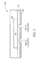
- Fig. 2 is a simplified cross-sectional diagram of an integrated circuit (IC) package 200 with stress releasing structure in accordance with a first embodiment of the present invention
- Fig. 3 is a simplified bottom view diagram of the IC package 200.
- the IC package 200 comprises: a metal plane 202, a substrate 204, an IC chip 206, and an IC fill layer 208.
- the metal plane 202 has 4 etching lines 210 for separating the metal plane 202 into 9 small metal plane areas 212 as shown in Fig. 3 , wherein the metal plane 202 can be a copper plane.
- the 4 etching lines 210 form 4 half cut lines in the metal plane 202 and the substrate 204 as shown in Fig. 2 .
- the substrate 204 is formed on metal layer 202.
- the IC chip 206 is formed on the substrate 204, and the IC fill layer 208 is formed around the IC chip 206.
- the above embodiment is only for an illustrative purpose and is not meant to be a limitation of the present invention.
- the number of the etching lines 210 can be changed according to different design requirements.
- Fig. 4 is a simplified cross-sectional diagram of an IC package 300 with stress releasing structure in accordance with a second embodiment of the present invention
- Fig. 5 is a simplified bottom view diagram of the IC package 300.
- the IC package 300 comprises: a metal plane 302, a substrate 304, an IC chip 306, an IC fill layer 308, and 2 bonding wires 309.
- the metal plane 302 has 4 etching lines 310 for separating the metal plane 302 into 9 small metal plane areas 312 as shown in Fig. 5 , wherein the metal plane 302 can be a copper plane.
- the substrate 304 is formed on metal layer 302, and the 4 etching lines 310 also separate the substrate 304 into 9 small substrate areas.
- the 4 etching lines 310 form 4 full cut lines in the metal plane 302 and the substrate 304 as shown in Fig. 4 .
- the IC chip 306 is formed on the substrate 304, and the IC fill layer 308 is formed around the IC chip 306.
- the above embodiment is only for an illustrative purpose and is not meant to be a limitation of the present invention.
- the number of the etching lines 310 can be changed according to different design requirements.
- Fig. 6 is a simplified cross-sectional diagram of an IC package 400 with stress releasing structure in accordance with a third embodiment of the present invention
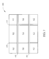
- Fig. 7 is a simplified bottom view diagram of the IC package 400
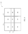
- Fig. 8 is a simplified top view diagram of the IC package 400.
- the IC package 400 comprises: a metal plane 402, a substrate 404, an IC chip 406, and an IC fill layer 408.
- the metal plane 402 has 4 first etching lines 410 for separating the metal plane 402 into 9 small metal plane areas 412 as shown in Fig. 7 , wherein the metal plane 402 can be a copper plane.
- the 4 first etching lines 410 form 4 half cut lines in the metal plane 402 and the substrate 404 as shown in Fig. 4 .
- the substrate 404 is formed on metal layer 404, and the IC chip 406 is formed on the substrate 404.
- the IC fill layer 408 is formed around the IC chip 406, and the IC fill layer 408 has 4 second etching lines 414 for separating the IC fill layer 408 into a plurality of areas as shown in Fig. 8 .
- the 4 second etching lines 414 form 4 half cut lines in the IC fill layer 408 as shown in Fig. 6 .
- the above embodiment is only for an illustrative purpose and is not meant to be a limitation of the present invention.
- the numbers of the first etching lines 410 and the second etching lines 414 can be changed according to different design requirements.
- Fig. 9 is a simplified cross-sectional diagram of an IC package 500 with stress releasing structure in accordance with a fourth embodiment of the present invention
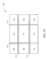
- Fig. 10 is a simplified bottom view diagram of the IC package 500
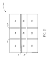
- Fig. 11 is a simplified top view diagram of the IC package 500.
- the IC package 500 comprises: a metal plane 502, a substrate 504, an IC chip 506, an IC fill layer 508, and 2 bonding wires 509.
- the metal plane 502 has 4 etching lines 510 for separating the metal plane 502 into 9 small metal plane areas 512 as shown in Fig.
- the metal plane 502 can be a copper plane.
- the substrate 504 is formed on metal layer 502, and the 4 etching lines 510 also separate the substrate 504 into 9 small substrate areas. In other words, the 4 etching lines 510 form 4 full cut lines in the metal plane 502 and the substrate 504 as shown in Fig. 9 .
- the IC chip 506 is formed on the substrate 504, and the IC fill layer 508 is formed around the IC chip 506.
- the IC fill layer 508 has 4 second etching lines 414 for separating the IC fill layer 408 into a plurality of areas as shown in Fig. 11 .
- the 4 second etching lines 414 form 4 half cut lines in the IC fill layer 408 as shown in Fig. 9 .
- the above embodiment is only for an illustrative purpose and is not meant to be a limitation of the present invention.
- the numbers of the first etching lines 510 and the second etching lines 514 can be changed according to different design requirements.
- the IC package with stress releasing structure disclosed by the present invention can separate the metal plane into a plurality of small metal planes in order to release stress, so as to solve the delamination problem of the IC package during a reflow process. All combinations and sub-combinations of the above-described features also belong to the invention.
Landscapes
- Internal Circuitry In Semiconductor Integrated Circuit Devices (AREA)
- Physics & Mathematics (AREA)
- Geometry (AREA)
- Semiconductor Integrated Circuits (AREA)
- Engineering & Computer Science (AREA)
- Microelectronics & Electronic Packaging (AREA)
- Lead Frames For Integrated Circuits (AREA)
Abstract
Description
- The present invention relates to IC packages with stress releasing structure according to the pre-characterizing clauses of claims 1 and 7.
- Please refer to
Fig. 1. Fig. 1 is aconventional IC package 100 during a reflow process. As shown inFig. 1 , theconventional IC package 100 comprises: acopper plane 102, asubstrate 104, anIC chip 106, and anIC fill layer 108. As shown inFig. 1 , after the reflow process, a delamination problem happens due to a large stress between thecopper plane 102, thesubstrate 104, and theIC chip 106, and theIC package 100 will fail due to the delamination problem. - This in mind, the present invention aims at providing an IC package with stress releasing structure.
- This is achieved by IC packages according to the independent claims 1 and 7. The respective dependent claims pertain to corresponding further developments and improvements.
- As will be seen more clearly from the detailed description following below, one claimed IC package includes: a metal plane, a substrate, an IC chip, and an IC fill layer. The metal plane has at least one first etching line for separating the metal plane into a plurality of areas. The substrate is formed on metal layer. The IC chip is formed on the substrate, and the IC fill layer is formed around the IC chip. The at least one first etching line forms at least one half cut line in the metal plane and the substrate.
- As will be seen more clearly from the detailed description following below, one claimed IC package includes: a metal plane, a substrate, at least one bonding wire, an IC chip, and an IC fill layer. The metal plane has at least one first etching line for separating the metal plane into a plurality of areas. The substrate is formed on metal layer, wherein the at least one first etching line separates the substrate into a plurality of substrate areas. The IC chip is formed on the substrate, and the IC fill layer is formed around the IC chip. The at least one first etching line forms at least one full cut line in the metal plane and the substrate.
- In the following, the invention is further illustrated by way of example, taking reference to the accompanying drawings. Thereof
-
Fig. 1 is a conventional IC package during a reflow process. -
Fig. 2 is a simplified cross-sectional diagram of an IC package with stress releasing structure in accordance with a first embodiment of the present invention. -
Fig. 3 is a simplified bottom view diagram of the IC package with stress releasing structure in accordance with a first embodiment of the present invention. -
Fig. 4 is a simplified cross-sectional diagram of an IC package with stress releasing structure in accordance with a second embodiment of the present invention. -
Fig. 5 is a simplified bottom view diagram of the IC package with stress releasing structure in accordance with a second embodiment of the present invention. -
Fig. 6 is a simplified cross-sectional diagram of an IC package with stress releasing structure in accordance with a third embodiment of the present invention. -
Fig. 7 is a simplified bottom view diagram of the IC package with stress releasing structure in accordance with a third embodiment of the present invention. -
Fig. 8 is a simplified top view diagram of the IC package with stress releasing structure in accordance with a third embodiment of the present invention. -
Fig. 9 is a simplified cross-sectional diagram of an IC package with stress releasing structure in accordance with a fourth embodiment of the present invention. -
Fig. 10 is a simplified bottom view diagram of the IC package with stress releasing structure in accordance with a fourth embodiment of the present invention. -
Fig. 11 is a simplified top view diagram of the IC package with stress releasing structure in accordance with a fourth embodiment of the present invention. - Certain terms are used throughout the description and following claims to refer to particular components. As one skilled in the art will appreciate, manufacturers may refer to a component by different names. This document does not intend to distinguish between components that differ in name but not function. In the following description and in the claims, the terms "include" and "comprise" are used in an open-ended fashion, and thus should be interpreted to mean "include, but not limited to ...". Also, the term "couple" is intended to mean either an indirect or direct electrical connection. Accordingly, if one device is coupled to another device, that connection may be through a direct electrical connection, or through an indirect electrical connection via other devices and connections.
- Please refer to
Fig. 2 andFig. 3 together.Fig. 2 is a simplified cross-sectional diagram of an integrated circuit (IC)package 200 with stress releasing structure in accordance with a first embodiment of the present invention, andFig. 3 is a simplified bottom view diagram of theIC package 200. As shown inFig. 2 , theIC package 200 comprises: ametal plane 202, asubstrate 204, anIC chip 206, and anIC fill layer 208. Themetal plane 202 has 4etching lines 210 for separating themetal plane 202 into 9 smallmetal plane areas 212 as shown inFig. 3 , wherein themetal plane 202 can be a copper plane. In other words, the 4etching lines 210 form 4 half cut lines in themetal plane 202 and thesubstrate 204 as shown inFig. 2 . Thesubstrate 204 is formed onmetal layer 202. TheIC chip 206 is formed on thesubstrate 204, and theIC fill layer 208 is formed around theIC chip 206. Please note that the above embodiment is only for an illustrative purpose and is not meant to be a limitation of the present invention. For example, the number of theetching lines 210 can be changed according to different design requirements. - Please refer to
Fig. 4 andFig. 5 together.Fig. 4 is a simplified cross-sectional diagram of anIC package 300 with stress releasing structure in accordance with a second embodiment of the present invention, andFig. 5 is a simplified bottom view diagram of theIC package 300. As shown inFig. 4 , theIC package 300 comprises: ametal plane 302, asubstrate 304, anIC chip 306, anIC fill layer 308, and 2bonding wires 309. Themetal plane 302 has 4etching lines 310 for separating themetal plane 302 into 9 smallmetal plane areas 312 as shown inFig. 5 , wherein themetal plane 302 can be a copper plane. Thesubstrate 304 is formed onmetal layer 302, and the 4etching lines 310 also separate thesubstrate 304 into 9 small substrate areas. In other words, the 4etching lines 310 form 4 full cut lines in themetal plane 302 and thesubstrate 304 as shown inFig. 4 . TheIC chip 306 is formed on thesubstrate 304, and theIC fill layer 308 is formed around theIC chip 306. Please note that the above embodiment is only for an illustrative purpose and is not meant to be a limitation of the present invention. For example, the number of theetching lines 310 can be changed according to different design requirements. - Please refer to
Fig. 6 ,Fig. 7 , andFig. 8 together.Fig. 6 is a simplified cross-sectional diagram of anIC package 400 with stress releasing structure in accordance with a third embodiment of the present invention, andFig. 7 is a simplified bottom view diagram of theIC package 400, andFig. 8 is a simplified top view diagram of theIC package 400. As shown inFig. 4 , theIC package 400 comprises: ametal plane 402, asubstrate 404, anIC chip 406, and anIC fill layer 408. - The
metal plane 402 has 4first etching lines 410 for separating themetal plane 402 into 9 smallmetal plane areas 412 as shown inFig. 7 , wherein themetal plane 402 can be a copper plane. In other words, the 4first etching lines 410 form 4 half cut lines in themetal plane 402 and thesubstrate 404 as shown inFig. 4 . Thesubstrate 404 is formed onmetal layer 404, and theIC chip 406 is formed on thesubstrate 404. TheIC fill layer 408 is formed around theIC chip 406, and theIC fill layer 408 has 4second etching lines 414 for separating theIC fill layer 408 into a plurality of areas as shown inFig. 8 . In other words, the 4second etching lines 414 form 4 half cut lines in theIC fill layer 408 as shown inFig. 6 . - Please note that the above embodiment is only for an illustrative purpose and is not meant to be a limitation of the present invention. For example, the numbers of the
first etching lines 410 and thesecond etching lines 414 can be changed according to different design requirements. - Please refer to
Fig. 9 ,Fig. 10 , andFig. 11 together.Fig. 9 is a simplified cross-sectional diagram of anIC package 500 with stress releasing structure in accordance with a fourth embodiment of the present invention, andFig. 10 is a simplified bottom view diagram of theIC package 500, andFig. 11 is a simplified top view diagram of theIC package 500. As shown inFig. 9 , theIC package 500 comprises: ametal plane 502, asubstrate 504, anIC chip 506, anIC fill layer 508, and 2bonding wires 509. Themetal plane 502 has 4etching lines 510 for separating themetal plane 502 into 9 smallmetal plane areas 512 as shown inFig. 10 , wherein themetal plane 502 can be a copper plane. Thesubstrate 504 is formed onmetal layer 502, and the 4etching lines 510 also separate thesubstrate 504 into 9 small substrate areas. In other words, the 4etching lines 510 form 4 full cut lines in themetal plane 502 and thesubstrate 504 as shown inFig. 9 . TheIC chip 506 is formed on thesubstrate 504, and theIC fill layer 508 is formed around theIC chip 506. - The
IC fill layer 508 has 4second etching lines 414 for separating theIC fill layer 408 into a plurality of areas as shown inFig. 11 . In other words, the 4second etching lines 414 form 4 half cut lines in theIC fill layer 408 as shown inFig. 9 . Please note that the above embodiment is only for an illustrative purpose and is not meant to be a limitation of the present invention. For example, the numbers of thefirst etching lines 510 and thesecond etching lines 514 can be changed according to different design requirements. - Briefly summarized, the IC package with stress releasing structure disclosed by the present invention can separate the metal plane into a plurality of small metal planes in order to release stress, so as to solve the delamination problem of the IC package during a reflow process. All combinations and sub-combinations of the above-described features also belong to the invention.
Claims (13)
- An integrated circuit (IC) package (200, 400) with stress releasing structure, comprising:a metal plane (202, 402), having at least one first etching line (210, 410) for separating the metal plane (202, 402) into a plurality of metal plane areas (212, 412);a substrate (204, 404), formed on metal layer;an IC chip (206, 406), formed on the substrate (204, 404); andan IC fill layer (208, 408), formed around the IC chip (206, 406);wherein the at least one first etching line (210, 410) forms at least one half cut line in the metal plane (202, 402) and the substrate (204, 404).
- The IC package (200, 400) of claim 1, wherein the at least one first etching line (210, 410) forms at least one half cut line to separate the entire metal plane (202, 402) and a portion of the substrate (204, 404).
- The IC package (400) of claim 1, wherein the IC fill layer (408) has at least one second etching line for separating the IC fill layer (408) into a plurality of areas.
- The IC package (400) of claim 3, wherein the at least one second etching line (414) forms at least one half cut line to separate a portion of the IC fill layer (408).
- The IC package (400) of claim 3, wherein the at least one second etching line (414) forms at least one half cut line to separate the entire IC fill layer (408).
- The IC package (200, 400) of claim 1, wherein the metal plane (202, 402) is a copper plane.
- An integrated circuit (IC) package (300, 500) with stress releasing structure, comprising:a metal plane (302, 502), having at least one first etching line for separating the metal plane (302, 502) into a plurality of metal plane areas (312, 512);a substrate (304, 504), formed on metal layer, wherein the at least one first etching line separates the substrate (304, 504) into a plurality of substrate (304, 504) areas;an IC chip (306, 506), formed on the substrate (304, 504); andan IC fill layer (308, 508), formed around the IC chip (306, 506);wherein the at least one first etching line forms at least one full cut line in the metal plane (302, 502) and the substrate (304, 504).
- The IC package (300, 500) of claim 7, wherein the at least one first etching line forms at least one half cut line to separate the entire metal plane (302, 502) and the entire substrate (304, 504).
- The IC package (300, 500) of claim 7, further comprising:at least one bonding wire (309, 509), coupled between the separated substrate (304, 504) areas.
- The IC package (500) of claim 7, wherein the IC fill layer (508) has at least one second etching line (514) for separating the IC fill layer (508) into a plurality of areas.
- The IC package (500) of claim 10, wherein the at least one second etching line (514) forms at least one half cut line to separate a portion of the IC fill layer (508).
- The IC package (500) of claim 10, wherein the at least one second etching line (514) forms at least one half cut line to separate the entire IC fill layer (508).
- The IC package (300, 500) of claim 10, wherein the metal plane (302, 502) is a copper plane.
Applications Claiming Priority (2)
| Application Number | Priority Date | Filing Date | Title |
|---|---|---|---|
| US201462034931P | 2014-08-08 | 2014-08-08 | |
| US14/686,783 US9905515B2 (en) | 2014-08-08 | 2015-04-15 | Integrated circuit stress releasing structure |
Publications (2)
| Publication Number | Publication Date |
|---|---|
| EP2983201A1 true EP2983201A1 (en) | 2016-02-10 |
| EP2983201B1 EP2983201B1 (en) | 2017-06-28 |
Family
ID=53758122
Family Applications (1)
| Application Number | Title | Priority Date | Filing Date |
|---|---|---|---|
| EP15178842.9A Active EP2983201B1 (en) | 2014-08-08 | 2015-07-29 | Integrated circuit package with stress releasing structure |
Country Status (4)
| Country | Link |
|---|---|
| US (1) | US9905515B2 (en) |
| EP (1) | EP2983201B1 (en) |
| CN (1) | CN105374761B (en) |
| TW (1) | TW201606958A (en) |
Families Citing this family (1)
| Publication number | Priority date | Publication date | Assignee | Title |
|---|---|---|---|---|
| US11127604B2 (en) * | 2018-01-05 | 2021-09-21 | Innolux Corporation | Manufacturing method of semiconductor device |
Citations (5)
| Publication number | Priority date | Publication date | Assignee | Title |
|---|---|---|---|---|
| WO2003073500A1 (en) * | 2002-02-28 | 2003-09-04 | Infineon Technologies Ag | A substrate for a semiconductor device |
| DE102006015241A1 (en) * | 2006-03-30 | 2007-06-28 | Infineon Technologies Ag | Semiconductor component with a plastic housing and partially embedded in plastic external contacts and method for producing the semiconductor device |
| US20080305306A1 (en) * | 2007-06-07 | 2008-12-11 | Cheemen Yu | Semiconductor molded panel having reduced warpage |
| DE102010054781A1 (en) * | 2010-12-16 | 2012-06-21 | Epcos Ag | Module for reducing thermomechanical stress on e.g. surface wave filters, has encapsulated components provided on support substrate, and encapsulation mass surrounding components, where encapsulation mass comprises material recess |
| WO2012165111A1 (en) * | 2011-05-31 | 2012-12-06 | 株式会社村田製作所 | Method for producing multi-layer substrate and multi-layer substrate |
Family Cites Families (25)
| Publication number | Priority date | Publication date | Assignee | Title |
|---|---|---|---|---|
| JPS57133655A (en) * | 1981-02-10 | 1982-08-18 | Pioneer Electronic Corp | Lead frame |
| US4918511A (en) * | 1985-02-01 | 1990-04-17 | Advanced Micro Devices, Inc. | Thermal expansion compensated metal lead frame for integrated circuit package |
| US5126820A (en) * | 1985-02-01 | 1992-06-30 | Advanced Micro Devices, Inc. | Thermal expansion compensated metal lead frame for integrated circuit package |
| US6204553B1 (en) * | 1999-08-10 | 2001-03-20 | Walsin Advanced Electronics Ltd. | Lead frame structure |
| US6979595B1 (en) * | 2000-08-24 | 2005-12-27 | Micron Technology, Inc. | Packaged microelectronic devices with pressure release elements and methods for manufacturing and using such packaged microelectronic devices |
| KR100652395B1 (en) * | 2005-01-12 | 2006-12-01 | 삼성전자주식회사 | Semiconductor element with suppressed die warpage and manufacturing method thereof |
| TWI259518B (en) | 2005-06-20 | 2006-08-01 | Advanced Semiconductor Eng | Method for forming leadless semiconductor packages |
| KR100652442B1 (en) * | 2005-11-09 | 2006-12-01 | 삼성전자주식회사 | Semiconductor chip and manufacturing method thereof |
| CN101385139B (en) * | 2005-12-21 | 2010-06-23 | 飞思卡尔半导体公司 | Lead frame based semiconductor package and method of making same |
| DE112006004099B4 (en) * | 2006-11-14 | 2013-08-22 | Infineon Technologies Ag | Electronic component and method for its production |
| CN100576478C (en) | 2007-09-29 | 2009-12-30 | 南茂科技股份有限公司 | Packaging method for crystal grain reconfiguration |
| US8084299B2 (en) | 2008-02-01 | 2011-12-27 | Infineon Technologies Ag | Semiconductor device package and method of making a semiconductor device package |
| US8053336B2 (en) * | 2008-11-12 | 2011-11-08 | Taiwan Semiconductor Manufacturing Company, Ltd. | Method for reducing chip warpage |
| KR101711479B1 (en) * | 2010-10-06 | 2017-03-03 | 삼성전자 주식회사 | Semiconductor package apparatus and its test system |
| KR101255930B1 (en) * | 2011-07-04 | 2013-04-23 | 삼성전기주식회사 | Power Module Package and Method for Manufacturing the same |
| CN102376671A (en) * | 2011-11-29 | 2012-03-14 | 杭州矽力杰半导体技术有限公司 | Lead frame and flip-chip type semiconductor packaging structure using the same |
| CN104012169B (en) * | 2011-12-27 | 2019-03-05 | 英特尔公司 | Method and system for coexistence of multiple co-located radios |
| US9318404B2 (en) * | 2013-02-05 | 2016-04-19 | Stats Chippac, Ltd. | Semiconductor device and method of forming stress relieving vias for improved fan-out WLCSP package |
| US9123712B1 (en) * | 2013-07-24 | 2015-09-01 | Stats Chippac Ltd. | Leadframe system with warp control mechanism and method of manufacture thereof |
| US9293409B2 (en) * | 2013-09-11 | 2016-03-22 | Infineon Technologies Ag | Method for manufacturing a semiconductor device, and semiconductor device |
| US9281256B2 (en) * | 2013-09-25 | 2016-03-08 | Freescale Semiconductor, Inc. | Package encapsulant relief feature |
| US9397019B2 (en) * | 2014-02-25 | 2016-07-19 | Intel IP Corporation | Integrated circuit package configurations to reduce stiffness |
| FR3018630A1 (en) * | 2014-03-11 | 2015-09-18 | St Microelectronics Grenoble 2 | PERFORATED ELECTRONIC HOUSING AND METHOD OF MANUFACTURE |
| US9859162B2 (en) * | 2014-09-11 | 2018-01-02 | Alta Devices, Inc. | Perforation of films for separation |
| US9214440B1 (en) * | 2014-12-17 | 2015-12-15 | Texas Instruments Incorporated | Method for preventing die pad delamination |
-
2015
- 2015-04-15 US US14/686,783 patent/US9905515B2/en active Active
- 2015-06-24 CN CN201510352969.XA patent/CN105374761B/en active Active
- 2015-07-29 EP EP15178842.9A patent/EP2983201B1/en active Active
- 2015-08-04 TW TW104125288A patent/TW201606958A/en unknown
Patent Citations (5)
| Publication number | Priority date | Publication date | Assignee | Title |
|---|---|---|---|---|
| WO2003073500A1 (en) * | 2002-02-28 | 2003-09-04 | Infineon Technologies Ag | A substrate for a semiconductor device |
| DE102006015241A1 (en) * | 2006-03-30 | 2007-06-28 | Infineon Technologies Ag | Semiconductor component with a plastic housing and partially embedded in plastic external contacts and method for producing the semiconductor device |
| US20080305306A1 (en) * | 2007-06-07 | 2008-12-11 | Cheemen Yu | Semiconductor molded panel having reduced warpage |
| DE102010054781A1 (en) * | 2010-12-16 | 2012-06-21 | Epcos Ag | Module for reducing thermomechanical stress on e.g. surface wave filters, has encapsulated components provided on support substrate, and encapsulation mass surrounding components, where encapsulation mass comprises material recess |
| WO2012165111A1 (en) * | 2011-05-31 | 2012-12-06 | 株式会社村田製作所 | Method for producing multi-layer substrate and multi-layer substrate |
Also Published As
| Publication number | Publication date |
|---|---|
| CN105374761A (en) | 2016-03-02 |
| TW201606958A (en) | 2016-02-16 |
| US20160043040A1 (en) | 2016-02-11 |
| CN105374761B (en) | 2019-08-23 |
| EP2983201B1 (en) | 2017-06-28 |
| US9905515B2 (en) | 2018-02-27 |
Similar Documents
| Publication | Publication Date | Title |
|---|---|---|
| CN105261611B (en) | Chip stack packaging structure and stack packaging method | |
| US20120139095A1 (en) | Low-profile microelectronic package, method of manufacturing same, and electronic assembly containing same | |
| US20150334823A1 (en) | Substrate components for packaging ic chips and electronic device packages of the same | |
| KR101570274B1 (en) | Through package via(tpv) | |
| US9673178B2 (en) | Method of forming package structure with dummy pads for bonding | |
| EP3032582A2 (en) | Structure and formation method of chip package structure | |
| US20130320463A1 (en) | Package structure having mems element and fabrication method thereof | |
| US9646941B2 (en) | Semiconductor packaging device including via-in pad (VIP) and manufacturing method thereof | |
| JP2009152503A (en) | Semiconductor device and manufacturing method thereof | |
| CN104979323A (en) | Quad flat no-lead package and manufacturing method thereof | |
| EP2983201B1 (en) | Integrated circuit package with stress releasing structure | |
| EP3340295A1 (en) | Packaging structure and fabrication method thereof | |
| US8927343B2 (en) | Package process | |
| US9490146B2 (en) | Semiconductor device with encapsulated lead frame contact area and related methods | |
| US9373526B2 (en) | Chip package and method for forming the same | |
| US9576912B1 (en) | Wafer level chip scale package (WLCSP) having edge protection | |
| US20150228625A1 (en) | Semiconductor package and method of manufacturing the same | |
| CN104471705B (en) | Low thermal stress for large-scale semiconductor chip encapsulates | |
| US8314501B2 (en) | Semiconductor chip package structure, semiconductor chip and semiconductor chip group | |
| US8556159B2 (en) | Embedded electronic component | |
| KR101516045B1 (en) | Printed circuit board and method of manufacturing the same | |
| KR20150067803A (en) | Semiconductor package structure for improving efficiency of thermal emission and method for fabricating the same | |
| US10074581B2 (en) | Chip package having a patterned conducting plate and a conducting pad with a recess | |
| JP2017092212A (en) | Semiconductor device and manufacturing method of the same | |
| KR20160085636A (en) | Semiconductor package structure and manufacturing method thereof |
Legal Events
| Date | Code | Title | Description |
|---|---|---|---|
| PUAI | Public reference made under article 153(3) epc to a published international application that has entered the european phase |
Free format text: ORIGINAL CODE: 0009012 |
|
| AK | Designated contracting states |
Kind code of ref document: A1 Designated state(s): AL AT BE BG CH CY CZ DE DK EE ES FI FR GB GR HR HU IE IS IT LI LT LU LV MC MK MT NL NO PL PT RO RS SE SI SK SM TR |
|
| AX | Request for extension of the european patent |
Extension state: BA ME |
|
| 17P | Request for examination filed |
Effective date: 20160701 |
|
| RBV | Designated contracting states (corrected) |
Designated state(s): AL AT BE BG CH CY CZ DE DK EE ES FI FR GB GR HR HU IE IS IT LI LT LU LV MC MK MT NL NO PL PT RO RS SE SI SK SM TR |
|
| GRAP | Despatch of communication of intention to grant a patent |
Free format text: ORIGINAL CODE: EPIDOSNIGR1 |
|
| RIC1 | Information provided on ipc code assigned before grant |
Ipc: H01L 23/31 20060101AFI20170203BHEP |
|
| INTG | Intention to grant announced |
Effective date: 20170301 |
|
| RAP1 | Party data changed (applicant data changed or rights of an application transferred) |
Owner name: MEDIATEK INC. |
|
| GRAS | Grant fee paid |
Free format text: ORIGINAL CODE: EPIDOSNIGR3 |
|
| GRAA | (expected) grant |
Free format text: ORIGINAL CODE: 0009210 |
|
| AK | Designated contracting states |
Kind code of ref document: B1 Designated state(s): AL AT BE BG CH CY CZ DE DK EE ES FI FR GB GR HR HU IE IS IT LI LT LU LV MC MK MT NL NO PL PT RO RS SE SI SK SM TR |
|
| REG | Reference to a national code |
Ref country code: GB Ref legal event code: FG4D |
|
| REG | Reference to a national code |
Ref country code: CH Ref legal event code: EP |
|
| REG | Reference to a national code |
Ref country code: AT Ref legal event code: REF Ref document number: 905546 Country of ref document: AT Kind code of ref document: T Effective date: 20170715 |
|
| REG | Reference to a national code |
Ref country code: IE Ref legal event code: FG4D |
|
| REG | Reference to a national code |
Ref country code: FR Ref legal event code: PLFP Year of fee payment: 3 |
|
| REG | Reference to a national code |
Ref country code: DE Ref legal event code: R096 Ref document number: 602015003300 Country of ref document: DE |
|
| PG25 | Lapsed in a contracting state [announced via postgrant information from national office to epo] |
Ref country code: HR Free format text: LAPSE BECAUSE OF FAILURE TO SUBMIT A TRANSLATION OF THE DESCRIPTION OR TO PAY THE FEE WITHIN THE PRESCRIBED TIME-LIMIT Effective date: 20170628 Ref country code: FI Free format text: LAPSE BECAUSE OF FAILURE TO SUBMIT A TRANSLATION OF THE DESCRIPTION OR TO PAY THE FEE WITHIN THE PRESCRIBED TIME-LIMIT Effective date: 20170628 Ref country code: LT Free format text: LAPSE BECAUSE OF FAILURE TO SUBMIT A TRANSLATION OF THE DESCRIPTION OR TO PAY THE FEE WITHIN THE PRESCRIBED TIME-LIMIT Effective date: 20170628 Ref country code: NO Free format text: LAPSE BECAUSE OF FAILURE TO SUBMIT A TRANSLATION OF THE DESCRIPTION OR TO PAY THE FEE WITHIN THE PRESCRIBED TIME-LIMIT Effective date: 20170928 Ref country code: GR Free format text: LAPSE BECAUSE OF FAILURE TO SUBMIT A TRANSLATION OF THE DESCRIPTION OR TO PAY THE FEE WITHIN THE PRESCRIBED TIME-LIMIT Effective date: 20170929 |
|
| REG | Reference to a national code |
Ref country code: NL Ref legal event code: MP Effective date: 20170628 |
|
| REG | Reference to a national code |
Ref country code: LT Ref legal event code: MG4D |
|
| REG | Reference to a national code |
Ref country code: AT Ref legal event code: MK05 Ref document number: 905546 Country of ref document: AT Kind code of ref document: T Effective date: 20170628 |
|
| PG25 | Lapsed in a contracting state [announced via postgrant information from national office to epo] |
Ref country code: LV Free format text: LAPSE BECAUSE OF FAILURE TO SUBMIT A TRANSLATION OF THE DESCRIPTION OR TO PAY THE FEE WITHIN THE PRESCRIBED TIME-LIMIT Effective date: 20170628 Ref country code: BG Free format text: LAPSE BECAUSE OF FAILURE TO SUBMIT A TRANSLATION OF THE DESCRIPTION OR TO PAY THE FEE WITHIN THE PRESCRIBED TIME-LIMIT Effective date: 20170928 Ref country code: SE Free format text: LAPSE BECAUSE OF FAILURE TO SUBMIT A TRANSLATION OF THE DESCRIPTION OR TO PAY THE FEE WITHIN THE PRESCRIBED TIME-LIMIT Effective date: 20170628 Ref country code: RS Free format text: LAPSE BECAUSE OF FAILURE TO SUBMIT A TRANSLATION OF THE DESCRIPTION OR TO PAY THE FEE WITHIN THE PRESCRIBED TIME-LIMIT Effective date: 20170628 Ref country code: NL Free format text: LAPSE BECAUSE OF FAILURE TO SUBMIT A TRANSLATION OF THE DESCRIPTION OR TO PAY THE FEE WITHIN THE PRESCRIBED TIME-LIMIT Effective date: 20170628 |
|
| PG25 | Lapsed in a contracting state [announced via postgrant information from national office to epo] |
Ref country code: SK Free format text: LAPSE BECAUSE OF FAILURE TO SUBMIT A TRANSLATION OF THE DESCRIPTION OR TO PAY THE FEE WITHIN THE PRESCRIBED TIME-LIMIT Effective date: 20170628 Ref country code: CZ Free format text: LAPSE BECAUSE OF FAILURE TO SUBMIT A TRANSLATION OF THE DESCRIPTION OR TO PAY THE FEE WITHIN THE PRESCRIBED TIME-LIMIT Effective date: 20170628 Ref country code: AT Free format text: LAPSE BECAUSE OF FAILURE TO SUBMIT A TRANSLATION OF THE DESCRIPTION OR TO PAY THE FEE WITHIN THE PRESCRIBED TIME-LIMIT Effective date: 20170628 Ref country code: RO Free format text: LAPSE BECAUSE OF FAILURE TO SUBMIT A TRANSLATION OF THE DESCRIPTION OR TO PAY THE FEE WITHIN THE PRESCRIBED TIME-LIMIT Effective date: 20170628 Ref country code: EE Free format text: LAPSE BECAUSE OF FAILURE TO SUBMIT A TRANSLATION OF THE DESCRIPTION OR TO PAY THE FEE WITHIN THE PRESCRIBED TIME-LIMIT Effective date: 20170628 |
|
| PG25 | Lapsed in a contracting state [announced via postgrant information from national office to epo] |
Ref country code: PL Free format text: LAPSE BECAUSE OF FAILURE TO SUBMIT A TRANSLATION OF THE DESCRIPTION OR TO PAY THE FEE WITHIN THE PRESCRIBED TIME-LIMIT Effective date: 20170628 Ref country code: ES Free format text: LAPSE BECAUSE OF FAILURE TO SUBMIT A TRANSLATION OF THE DESCRIPTION OR TO PAY THE FEE WITHIN THE PRESCRIBED TIME-LIMIT Effective date: 20170628 Ref country code: IT Free format text: LAPSE BECAUSE OF FAILURE TO SUBMIT A TRANSLATION OF THE DESCRIPTION OR TO PAY THE FEE WITHIN THE PRESCRIBED TIME-LIMIT Effective date: 20170628 Ref country code: IS Free format text: LAPSE BECAUSE OF FAILURE TO SUBMIT A TRANSLATION OF THE DESCRIPTION OR TO PAY THE FEE WITHIN THE PRESCRIBED TIME-LIMIT Effective date: 20171028 Ref country code: SM Free format text: LAPSE BECAUSE OF FAILURE TO SUBMIT A TRANSLATION OF THE DESCRIPTION OR TO PAY THE FEE WITHIN THE PRESCRIBED TIME-LIMIT Effective date: 20170628 |
|
| REG | Reference to a national code |
Ref country code: DE Ref legal event code: R097 Ref document number: 602015003300 Country of ref document: DE |
|
| PG25 | Lapsed in a contracting state [announced via postgrant information from national office to epo] |
Ref country code: MC Free format text: LAPSE BECAUSE OF FAILURE TO SUBMIT A TRANSLATION OF THE DESCRIPTION OR TO PAY THE FEE WITHIN THE PRESCRIBED TIME-LIMIT Effective date: 20170628 |
|
| PG25 | Lapsed in a contracting state [announced via postgrant information from national office to epo] |
Ref country code: DK Free format text: LAPSE BECAUSE OF FAILURE TO SUBMIT A TRANSLATION OF THE DESCRIPTION OR TO PAY THE FEE WITHIN THE PRESCRIBED TIME-LIMIT Effective date: 20170628 |
|
| REG | Reference to a national code |
Ref country code: IE Ref legal event code: MM4A |
|
| REG | Reference to a national code |
Ref country code: BE Ref legal event code: MM Effective date: 20170731 |
|
| PLBE | No opposition filed within time limit |
Free format text: ORIGINAL CODE: 0009261 |
|
| STAA | Information on the status of an ep patent application or granted ep patent |
Free format text: STATUS: NO OPPOSITION FILED WITHIN TIME LIMIT |
|
| 26N | No opposition filed |
Effective date: 20180329 |
|
| PG25 | Lapsed in a contracting state [announced via postgrant information from national office to epo] |
Ref country code: LU Free format text: LAPSE BECAUSE OF NON-PAYMENT OF DUE FEES Effective date: 20170729 |
|
| REG | Reference to a national code |
Ref country code: FR Ref legal event code: PLFP Year of fee payment: 4 |
|
| PG25 | Lapsed in a contracting state [announced via postgrant information from national office to epo] |
Ref country code: IE Free format text: LAPSE BECAUSE OF NON-PAYMENT OF DUE FEES Effective date: 20170729 |
|
| PG25 | Lapsed in a contracting state [announced via postgrant information from national office to epo] |
Ref country code: BE Free format text: LAPSE BECAUSE OF NON-PAYMENT OF DUE FEES Effective date: 20170731 Ref country code: SI Free format text: LAPSE BECAUSE OF FAILURE TO SUBMIT A TRANSLATION OF THE DESCRIPTION OR TO PAY THE FEE WITHIN THE PRESCRIBED TIME-LIMIT Effective date: 20170628 |
|
| PG25 | Lapsed in a contracting state [announced via postgrant information from national office to epo] |
Ref country code: MT Free format text: LAPSE BECAUSE OF NON-PAYMENT OF DUE FEES Effective date: 20170729 |
|
| REG | Reference to a national code |
Ref country code: CH Ref legal event code: PL |
|
| PG25 | Lapsed in a contracting state [announced via postgrant information from national office to epo] |
Ref country code: CH Free format text: LAPSE BECAUSE OF NON-PAYMENT OF DUE FEES Effective date: 20180731 Ref country code: LI Free format text: LAPSE BECAUSE OF NON-PAYMENT OF DUE FEES Effective date: 20180731 |
|
| PG25 | Lapsed in a contracting state [announced via postgrant information from national office to epo] |
Ref country code: HU Free format text: LAPSE BECAUSE OF FAILURE TO SUBMIT A TRANSLATION OF THE DESCRIPTION OR TO PAY THE FEE WITHIN THE PRESCRIBED TIME-LIMIT; INVALID AB INITIO Effective date: 20150729 |
|
| PG25 | Lapsed in a contracting state [announced via postgrant information from national office to epo] |
Ref country code: CY Free format text: LAPSE BECAUSE OF FAILURE TO SUBMIT A TRANSLATION OF THE DESCRIPTION OR TO PAY THE FEE WITHIN THE PRESCRIBED TIME-LIMIT Effective date: 20170628 |
|
| PG25 | Lapsed in a contracting state [announced via postgrant information from national office to epo] |
Ref country code: MK Free format text: LAPSE BECAUSE OF FAILURE TO SUBMIT A TRANSLATION OF THE DESCRIPTION OR TO PAY THE FEE WITHIN THE PRESCRIBED TIME-LIMIT Effective date: 20170628 |
|
| PG25 | Lapsed in a contracting state [announced via postgrant information from national office to epo] |
Ref country code: TR Free format text: LAPSE BECAUSE OF FAILURE TO SUBMIT A TRANSLATION OF THE DESCRIPTION OR TO PAY THE FEE WITHIN THE PRESCRIBED TIME-LIMIT Effective date: 20170628 |
|
| PG25 | Lapsed in a contracting state [announced via postgrant information from national office to epo] |
Ref country code: PT Free format text: LAPSE BECAUSE OF FAILURE TO SUBMIT A TRANSLATION OF THE DESCRIPTION OR TO PAY THE FEE WITHIN THE PRESCRIBED TIME-LIMIT Effective date: 20170628 |
|
| PG25 | Lapsed in a contracting state [announced via postgrant information from national office to epo] |
Ref country code: AL Free format text: LAPSE BECAUSE OF FAILURE TO SUBMIT A TRANSLATION OF THE DESCRIPTION OR TO PAY THE FEE WITHIN THE PRESCRIBED TIME-LIMIT Effective date: 20170628 |
|
| P01 | Opt-out of the competence of the unified patent court (upc) registered |
Effective date: 20230607 |
|
| PGFP | Annual fee paid to national office [announced via postgrant information from national office to epo] |
Ref country code: GB Payment date: 20250605 Year of fee payment: 11 |
|
| PGFP | Annual fee paid to national office [announced via postgrant information from national office to epo] |
Ref country code: FR Payment date: 20250610 Year of fee payment: 11 |
|
| PGFP | Annual fee paid to national office [announced via postgrant information from national office to epo] |
Ref country code: DE Payment date: 20250604 Year of fee payment: 11 |
|
| REG | Reference to a national code |
Ref country code: DE Ref legal event code: R079 Ref document number: 602015003300 Country of ref document: DE Free format text: PREVIOUS MAIN CLASS: H01L0023310000 Ipc: H10W0074100000 |