EP2980983A1 - Method for discharging capacitive loads - Google Patents
Method for discharging capacitive loads Download PDFInfo
- Publication number
- EP2980983A1 EP2980983A1 EP15183697.0A EP15183697A EP2980983A1 EP 2980983 A1 EP2980983 A1 EP 2980983A1 EP 15183697 A EP15183697 A EP 15183697A EP 2980983 A1 EP2980983 A1 EP 2980983A1
- Authority
- EP
- European Patent Office
- Prior art keywords
- inductor
- switch
- source
- voltage
- current
- Prior art date
- Legal status (The legal status is an assumption and is not a legal conclusion. Google has not performed a legal analysis and makes no representation as to the accuracy of the status listed.)
- Granted
Links
Images

Classifications
-
- H—ELECTRICITY
- H02—GENERATION; CONVERSION OR DISTRIBUTION OF ELECTRIC POWER
- H02N—ELECTRIC MACHINES NOT OTHERWISE PROVIDED FOR
- H02N2/00—Electric machines in general using piezoelectric effect, electrostriction or magnetostriction
- H02N2/18—Electric machines in general using piezoelectric effect, electrostriction or magnetostriction producing electrical output from mechanical input, e.g. generators
- H02N2/181—Circuits; Control arrangements or methods
Definitions
- This invention relates generally to electrical energy storage and more specifically, to storing the energy discharged from a capacitive load.
- Piezoelectric transducers are made of materials which possess the property of being able to transform mechanical forces into an output electrical energy. In a piezoelectric device, positive and negative electrical charges are separated when the material from which the device is made undergoes strain and a voltage is generated across the material.
- the amplitude of the generated electrical signal is a function of the size of the piezoelectric device and the level of strain or stress applied to it.
- the frequency of the generated electrical signal is a function of the frequency of the stress and strain to which the piezoelectric device is subjected.
- an oscillatory strain such as a vibration
- the amplitude and frequency of the generated signal may vary considerably depending on the material itself and the ability of the device to couple mechanical vibrations into stain within the piezoelectric device.
- Particular embodiments of the present invention include methods for storing electrical energy discharged from a capacitive source. Such methods include developing a capacitive load in the source and closing a switch between the capacitive source and a voltage conversion block after an output voltage of the source both exceeds a threshold value and is detected to peak.
- the conversion block includes an inductor and the storage device connected in series and further may include a diode connected in parallel across the inductor and the storage device.
- Such methods may further include opening the switch after a predetermined period of time and transferring the electrical energy within the voltage conversion block from an inductor to a storage device.
- Particular embodiments of such methods include, in addition to developing a capacitive load in the source, closing a switch between the capacitive source and a voltage conversion block after an output voltage of the source is determined to exceed a threshold value and opening the switch as the current through an inductor of the voltage conversion block is determined to reach a target value.
- Such methods may further include transferring the electrical energy within the voltage conversion block from the inductor to a storage device.
- Particular embodiments of the present invention include apparatus for storing electrical energy discharged from a capacitive source.
- Such apparatus include a capacitive source configured to produce an output voltage, a switch connected to the source, an inductor connected to the switch, a storage device connected to the inductor and a controller configured to close the switch after an output voltage of the source both exceeds a threshold value and is detected to peak.
- Harvested energy from an electrical energy source can be used to power a wide array of apparatus. If such harvested energy is not used immediately to power an apparatus, the electrical energy may be stored in a storage device such as, for example, a capacitor or a rechargeable battery. One or more apparatus may then draw upon the stored energy from the storage device as and when needed.
- a storage device such as, for example, a capacitor or a rechargeable battery.
- One or more apparatus may then draw upon the stored energy from the storage device as and when needed.
- the present invention includes methods and apparatus for storing electrical energy discharged from an electrical energy source of a capacitive nature to an energy storage device.
- the source of the electrical energy may include any source of a capacitive nature.
- Such capacitive sources may include, for example, a piezoelectric transducer or a capacitor. While much of the discussion that follows focuses on the example of a piezoelectric device as the capacitive source, it is recognized that the invention is not so limited.
- the methods and apparatus disclosed herein are particularly useful with, though not limited to, a capacitive source that provides a low amount of electrical energy, e.g ., from a piezoelectric transducer mounted inside of a tire.
- the amount of energy collected due to piezoelectric transduction is dependent upon the ability to transfer the voltage difference across the piezoelectric material into a storage medium. If the voltage is allowed to rise and fall with vibrations, however, energy may not be collected.
- the methods and apparatus disclosed herein are further particularly useful with, though not limited to, a capacitive source that produces random or scattered voltage peaks, i.e ., some peaks very high and other peaks quite low relative to one another and with other peaks scattered randomly throughout.
- Particular embodiments of the present invention include methods and apparatus that transfer the electrical energy at or near its peak voltage so that a greater amount of electrical energy is recovered and stored in the storage device.
- Arrangements to store the greater amount of electrical energy from the capacitive source include the source connected through a switch to a voltage conversion block.
- the voltage conversion block includes an inductor and the storage device. The switch is then opened and closed at optimum times so that the electrical energy can transfer from the capacitive source through the switch to the inductor and then to the storage device.
- the method includes closing the switch between the capacitive source and the voltage conversion block after the output voltage of the source exceeds a threshold value AND as the output voltage of the source is detected to peak. Closing the switch when the output voltage both exceeds the threshold value and reaches a peak is particularly useful with, but not limited to, embodiments of methods that are performed with a capacitive load having output voltage peaks that vary in value randomly, with high and low peaks relative one to the other.
- the voltage stored in the capacitive source is applied entirely across the inductor of the voltage conversion block. Because power is the time rate of change of energy, an instantaneous change in energy would require an infinite power. This instantaneous change in energy is contrary to standard notions of physical systems as the energy stored in any element of a system must be a continuous function of time. Because energy stored in an inductance is proportional to the square of the current, immediately after the switch is closed, the voltage is dropped across the inductor and no current immediately flows. As current does begin to flow through the inductor across the switch, the voltage drops in the source and the voltage increases in the storage device.
- Particular embodiments further include opening the switch at a predetermined time. At the point of opening the switch, particular embodiments provide that approximately half of the energy from the capacitive source is stored in the storage device and half is stored in the inductor. After the switch is opened, the electrical energy that is stored in the inductor at that time transfers to the storage device as the capacitive source again starts to build to a peak value. Particular embodiments of methods therefore include transferring the electrical energy within the voltage conversion block from the inductor to the storage device.
- the switch between the capacitive source and the voltage conversion block is closed and opened by a controller.
- Any controller including both analogue controllers and digital controllers, known to one having ordinary skill in the art that is capable of performing the functions described herein would be suitable for use in embodiments of the present invention.
- the controller may, for example, detect the peak voltage value of the capacitive source and/or determine that the output voltage of the capacitive source exceeds a threshold value and/or determines a time that a voltage peak of the source may be expected to occur and further would be capable of opening and closing the one or more switches at the proper times as included in particular embodiments. Examples of suitable controllers are provided below and more particularly, in the figures.
- Particular embodiments may further include comparing the output voltage of the source with a threshold value and determining that the output voltage exceeds the threshold value since one of the determinants for closing the switch is that the output voltage of the source exceeds the threshold valued.
- particular embodiments may further include closing a second switch as the output voltage of the source exceeds that threshold value and sending a signal through the closed second switch as the output voltage of the source is detected to peak.
- the embodiments may further include receiving the signal by the first switch as an instruction to close. In this manner, the switch between the capacitive load and the inductor of the voltage conversion block receives a signal to close after the controller has determined both that the output voltage of the source exceeds the threshold value AND the output voltage of the source has been detected to peak.
- after the second switch is opened before the predetermined period of time that opens the switch between the source and the inductor.
- Particular embodiments for storing electrical energy discharged from a capacitive source in addition to developing a capacitive load in the source, may further include closing the switch between the capacitive load and the voltage conversion block after the output voltage of the source is determined to exceed a threshold value.
- These embodiments are particularly useful with, but not limited to, embodiments of methods that are performed with a capacitive load having output voltage peaks that are quite similar in value.
- particular embodiments may further include a controller that is capable of opening the switch by comparing a value of the inductor current with a second reference value and determining that the current through the inductor has reached a target value as the value of the inductor current exceeds the second reference value.
- Particular embodiments may determine that the switch should opened by calculating a time when a value of the inductor current is expected to reach the target value and determining that the current through the inductor has reached the target value at the calculated time.
- Particular embodiments of methods of the present invention may further include rectifying the electrical energy from the capacitive source. It is noted that the electrical energy may be full-wave rectified or only partially rectified.
- Particular embodiments of the present invention further include apparatus for storing electrical energy discharged from a capacitive source.
- Particular embodiments of such apparatus include a source connection configured to connect to the capacitive source. Any connection known to one having ordinary skill in the art that is suitable for connecting to the capacitive source is acceptable for use with the present invention.
- source connections may include, for example, wires, cables, plugs, sockets, terminals, ports, printed circuits or combinations thereof.
- Particular embodiments may further include the capacitive source configured to produce an output voltage in a connected configuration with the source connection.
- apparatus further include a switch connected to the capacitive source, an inductor connected to the switch, a storage device connected to the inductor and a controller configured to close the switch as an output voltage of the source both exceeds a threshold value and is detected to peak.
- a switch connected to the capacitive source, an inductor connected to the switch, a storage device connected to the inductor and a controller configured to close the switch as an output voltage of the source both exceeds a threshold value and is detected to peak.
- Particular embodiments may further include a diode connected in parallel across the inductor and the storage device. The switch separates the transduction block from the voltage conversion block.
- particular embodiments of the apparatus have an inductor that has a value greater than C 1 2 ⁇ i s V 1 ⁇ ⁇ 2 wherein C I is the capacitive value of the storage device, i s is the saturation current of the inductor, and V I is the maximum voltage output value of the electrical energy source.
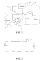
- FIG. 1 illustrates an exemplary embodiment of a transducer circuit providing energy collection.
- a piezoelectric transducer 1 produces an output voltage between two output terminals 2, 4 .
- a full-wave rectifier network 3 consists of, as is well known by one having ordinary skill in the art, four diodes D1, D2, D3, and D4 arranged in the rectifier network 3 .
- the piezoelectric transducer 1 may be formed from many different materials, may have many different shapes, and may be stressed in many different ways including, but not limited to, being shocked, twisted, stretched and squeezed or combinations thereof to produce an electrical signal, i.e ., an output voltage across the two output terminals 2, 4 .
- the rectifier network 3 includes two input terminals electrically connected to the output terminals 2, 4 of the piezoelectric transducer 1.
- the rectifier network 3 further includes two output terminals 8, 10 .
- the anode of diode D1 and the cathode of diode D4 are connected to the first terminal 2 of the piezoelectric transducer 1 while the cathodes of diodes D1 and D3 are connected to the first output terminal 8 of the rectifier network 3 .
- the anodes of diodes D2 and D4 are connected to the second output terminal 10 of the rectifier network 3 and the cathode of diode D2 and the anode of diode D3 are connected to second output terminal 4 of the piezoelectric transducer 1.
- a positive going signal produced by the piezoelectric transducer 1 causes a current to flow from terminal 2 via diode D1 into terminal 8 and via a load connected between the two output terminals 8, 10 of the rectifier network 3 and then via diode D2 into the second output terminal 4 of the piezoelectric transducer 1 .
- a negative going signal produced by the piezoelectric transducer 1 causes a current to flow from the second output terminal 4 of the piezoelectric transducer 1 via diode D3 into the first output terminal 8 of the rectifier network and then from the first output terminal 8 of the rectifier network into the second output terminal 10 of the rectifier network 3 by way of an electrical load connected between the two terminals and then via diode D4 into the first terminal 2 of the piezoelectric transducer 1 .
- the signal which is produced at the first output terminal 8 of the rectifier network 3 will always be at positive voltage with respect to the voltage at the second output terminal 10 of the rectifier network 3 .
- the circuit of FIG. 1 further includes a switch S1 that controls the flow of energy from the piezoelectric transducer 1 through the energy storage circuit by way of the controller 20 .
- the switch S1 may take many forms including, but not limited to, relay type switching devices and solid state devices.
- the switch S1 is electrically connected between the first output terminal 8 of the rectifier network 3 and one end of an inductor L1 .
- the other end of inductor L1 is connected to one end of a storage capacitor C1 .
- the other end of storage capacitor C1 is connected to the second output terminal 10 of the rectifier network 3 .
- Particular embodiments further include a diode D5 connected by its anode to the second output terminal 10 of the rectifier network 3 and by its cathode to a junction point between the switch S1 and inductor L1 .
- the switch S1 is closed, i.e ., made electrically conductive, by operation of the controller 20 upon sensing by the controller 20 via a line 22 of a voltage that is recognized by the controller 20 as corresponding generally to a condition that the output voltage across the piezoelectric transducer 1 both (1) exceeds a threshold value AND (2) is detected to peak as will be described in more detail below.
- Closing the switch S1 by the signal sent from the controller 20 permits discharge of the capacitive load of the piezoelectric transducer 1 , through the switch S1 and the inductor L1 to the storage capacitor C1 .
- the controller 20 is configured to open the switch S1 after a predetermined period of time.
- the controller 20 may close the switch S1 after the output voltage of the piezoelectric transducer 1 is determined to exceed a threshold value and may close the open the switch S1 by sensing current through the inductor L1 via a current sensor (not shown) connected to the outlet of the inductor L1 through a sensing line between the controller 20 and the current sensor.
- a current sensor not shown
- the diode D5 will be reverse-biased and substantially no current is allowed to flow through the diode D5 to the second output terminal 10 of the rectifier network 3 .
- the switch S1 opens by operation of the controller 20 (as described with the examples shown in FIGS. 4 and 5 with more detail below), current flow continues from the inductor L1 into the storage capacitor C1 with a return path through the diode D5 to transfer electrical energy within the inductor L1 to the storage device C1 .
- Energy stored in the storage device i.e ., the capacitor C1
- the capacitor C1 is proportional to the capacitance multiplied by the square of the voltage. In the case where the voltage across the storage element C1 is doubled, the stored energy will increase by a factor of 4.
- the piezoelectric transducer 1 considered as a capacitor, has the maximum available energy at the peak voltage. Therefore, energy may be transferred from the piezoelectric transducer 1 to the capacitor C1 by way of the switch S1 and the inductor L1 by configuring the controller 20 to close the switch S1 as the output voltage of the piezoelectric transducer 1 is near or at the maximum voltage across the transducer 1 .
- the controller 20 may close the switch S1 at 90 percent of the maximum voltage across the piezoelectric transducer 1 during the period. As the switch S1 closes, the voltage stored in the piezoelectric transducer 1 is applied entirely across inductor L1 .
- the diode D5 is chosen to minimize the junction capacitance since the inductor L1 , the capacitor C1 and the junction capacitance of the diode D5 form a tank circuit after the switch S1 is opened. Given the parasitic resistance of the circuit, a certain fraction of the oscillatory energy transferred from the diode D5 and the capacitor C1 will be lost as heat. Therefore, the tank circuit described must be critically damped by design.
- Particular embodiments include apparatus and methods that are useful in a tire to power electronic devices contained in or about the tire.
- Such an embodiment may include a piezoelectric transducer as the capacitive source that develops a capacitive load through the deflection of the piezoelectric transducer by the tire rotation.
- the generation of electrical energy from a piezoelectric transducer in a tire is well known in the art.
- the methods and apparatus disclosed herein are useful for maximizing the collection of the energy from such a piezoelectric transducer.
- the energy generated by the discharged capacitive load can be stored, for example, in a battery or capacitor as disclosed herein. This stored energy may then be used, for example, by a tire pressure sensor and/or a transmitter for transmitting information regarding the tire condition.
- FIG. 2 illustrates a simplified representation of the circuit of FIG. 1 .
- the circuit illustrated in FIG. 1 may be substantially simplified. If the discharge time is relatively short compared to the period of the vibrations induced in piezoelectric transducer 1 , neither the rectifier network 3 , the vibrational field nor the diode D5 need be considered between the time that the switch S1 is closed and the time it is opened since it may be assumed that all of these elements are in quasi-static states. In the circuit illustrated in FIG. 2 , the piezoelectric transducer 1 and the rectifier network 3 have been lumped as a single ideal capacitance Cp . The diode D5 has been eliminated since it will be reverse-biased from the time the switch S1 is closed until it is opened.
- V Cp Q 0 - Q t C p
- V C ⁇ 1 Q t C 1
- Q(t) is defined as the charge as a function of time and implicitly assumes that charge is conserved in the circuit
- Q 0 is defined as the initial charge on C p .
- a ratio ⁇ may be defined as the ratio of the ideal capacitance Cp to the capacitance of the storage device capacitor C1.
- C1 ⁇ Cp
- Equations ( 6 ) and (7) can be rewritten using this ratio as follows:
- Q t Q 0 ⁇ ⁇ ⁇ C p 1 + ⁇ ⁇ 1 - Cos ⁇ t ⁇ 1 - ⁇ ⁇ ⁇ C p ⁇ L 1
- i t Q 0 ⁇ ⁇ 1 + ⁇ ⁇ C p ⁇ L 1 ⁇ Sin ⁇ t ⁇ 1 + ⁇ ⁇ ⁇ C p ⁇ L 1 Equations ( 8 ) and ( 9 ) are therefore the complete solutions of charge and current in the simplified discharge circuit as a function of time after the switch is closed.
- Equation ( 10 ) Given a stopping time for the discharge process as shown in Equation ( 10 ), an estimate of the energy in each component of the simplified circuit starting with the piezoelectric capacitor, Cp.
- C P 2 C p 2 ⁇ Q 0 - a b
- C P 2 Q 0 2 2 ⁇ C p 1 - ⁇ 1 + ⁇ 2
- Equation ( 11 ) evaluates the function Q(t) at the time given by Equation ( 10 ) and using Equations ( 6 ) and ( 8 ). The calculation is simplified since the argument of the cos function reduces to 0. The result in Equation ( 11 ) gives a simple expression for the amount of energy remaining in the device, Cp, after the discharge period.
- the method of the present invention may be used to calculate a time when a value of the inductor current is expected to reach a peak or target value and one may then recognize that calculated value as the peak value of the inductor current and operate switch S1 in accordance with those calculations.
- the task becomes one of searching out components which satisfy the constraints of Equation ( 16 ) for a given piezoelectric capacitance and a given maximum piezoelectric voltage. For example, consider an 80 nF piezoelectric capacitance and a 30V output. If the saturation current is 1.2A, the inductor must be at least 123 uH to satisfy Equation ( 16 ).
- FIG. 3 diagrammatically illustrates a general circuit topology for performing energy conservation.
- the exemplary circuit topology for performing energy conversion illustrates the control of the switch between the energy transduction block and the energy conversion block.
- the conversion circuit is broken into five operational blocks which partition system function.
- the first three, the energy transduction, voltage conversion, and sense Vmax/Imax control blocks make up a voltage converter, although in this embodiment, it is a single cycle device.
- the illustration of the use of a buck converter indicates that small numbers of electrons at a higher potential have been produced and it is desired to convert these into a larger number of electrons at a lower potential.
- the energy storage and voltage transfer controls also illustrated in FIG. 3 determine how the energy is to be used and managed and are not required for conversion.
- a significant aspect of the operation of particular embodiments of the present invention is determining when the output voltage from the capacitive source, for example a piezoelectric device, has reached a value that triggers the switch between the transduction block and the voltage conversion block to open and/or close.
- Two examples of voltage sensing devices useful for this aspect are a threshold detector, which may be configured to close the switch S1 whenever the voltage on the piezoelectric device exceeds a specified or predetermined value and a peak detector which finds each peak using, for example, a zero crossing detector configuration. It will be appreciated by those of ordinary skill in the art that there are other controllers that can accomplish this task including, without limitation, circuits, solid state devices, analogue controllers, digital controllers and combinations thereof.
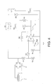
- FIG. 4 illustrates an exemplary voltage threshold detector that may be employed in the performance of certain embodiments.
- resistors R1 and R2 form a voltage divider as one input to operational amplifier U2 .
- the values for resistors R1 and R2 are chosen to minimize loss via current to ground as well as to provide an adequate input range into the operational amplifier U2 .
- One example of a design process using this threshold detector would be to choose a leakage current through the voltage divider network formed by resistors R1 and R2 to be in the range of multiples of 10 nAmperes and to begin the capacitive discharge of the transducer block at no more than 29 volts under maximum tolerance extremes with a 1.25V reference into the inverting input of the operational amplifier U2 .
- the operation of the threshold comparator illustrated in FIG. 4 is as follows.
- the output of the operational amplifier U2 drives a digital control signal into the switch S1 , causing the switch S1 to close.
- the switch S1 may be, for example, a solid state switching device.
- the transduction block connects to the voltage conversion block allowing the capacitive load of the piezoelectric transducer 1 to discharge into the inductor L1 as described previously.
- the output of operational amplifier U2 drops back to zero.
- the capacitor C2 , the diode D6 and the resistor R6 control the shape of the input pulse from the output of operational amplifier U2 into the digital input of switch S1 in such a way that there is a designated persistence even after the output of operational amplifier U2 has dropped to zero.
- the capacitor C1 is the parasitic capacitance of the solid state switch S1 and the resistor R6 is chosen so that the RC time constant of the switch S1 and the resistor cause persistence or hysteresis in the actuation of the switch S1 .
- the switch S1 closed and opens only after the period of time set by shaped input pulse from the operational amplifier U2 .
- Resistors R3, R4 and R5 are used to control the hysteresis bandwidth of the operational amplifier U2 to prevent coupled noise from affecting the output state.
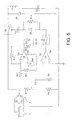
- FIG. 5 illustrates both an exemplary voltage peak detector and voltage threshold detector that may be combined in the performance of certain embodiments.
- a threshold detector includes the operational amplifier U4 and a zero crossing detector used as a peak detector includes operational amplifier U3 .
- the signal into the inverting (-) input of the operational amplifier U3 is from the output of a common analog differentiator formed by the resistor R9 and the capacitor C4 .
- the input of the differentiator is chosen as the voltage formed by the divider consisting of resistors R7 and R8 .
- the input of the divider is also used at the non-inverting (+) input of the operational amplifier U4 , which is included in the threshold detector.
- the operation of the threshold detector of FIG. 5 is similar to that described in FIG. 4 except that the output of the operational amplifier U4 if FIG. 5 drives the AND switch S2 .
- the divider conditions the voltage so as not to exceed the input rails of operational amplifier U4 .
- the operational amplifier U4 must be realized using high-value resistors to minimize current to ground from the output of the rectifier network 3 .
- the magnitude of the built-in reference V will constrain the divider ratio formed by the resistors R7, R8 .
- the values of the capacitor C4 and the resistor R9 are chosen so that the RC time constant is in the range of twenty (20) times the longest period of input to rectifier network 3 from the transduction block and to provide enough frequency bandwidth to operate optimally over the frequency range required.
- the peak detector which includes operational amplifier U3 , is designed to find the points where the rectified voltage is changing from increasing to decreasing, that is, the voltage extremum.
- a zero-crossing detector can be used to indicate the peak.
- the output of the zero-crossing detector is combined by means of the logical AND operator (the switch S2 ) with the output of the threshold detector which constrains a voltage level on the rectified signal.
- the logical AND is accomplished by using the output of the threshold detector as the control voltage for the switch S2 .
- the zero-crossing detector output which forms the control voltage for switch S1 , is logically true only when the rectified signal is of a sufficient voltage level AND is at an extremum.
- the output voltage of operational amplifier U3 is used to control the digital input of the switch S1 , which closes the switch S1 and connects the transduction block and the voltage conversion block.
- the reason for combining the threshold detector output with the output of the zero-crossing detector by means of a logical AND is to prevent the system from latching open under indeterminate conditions such as those likely to be induced during transduction block discharge. Further, the choice of threshold condition, proper design of the hysteresis bandwidth of operational amplifier U4, and the shape of the control voltage (diode D8, capacitor C3 and resistor R14) at the switch S1 allow for design control of the discharge properties of the transduction block into the voltage conversion block.
Landscapes
- Dc-Dc Converters (AREA)
- Charge And Discharge Circuits For Batteries Or The Like (AREA)
Abstract
Description
- This invention relates generally to electrical energy storage and more specifically, to storing the energy discharged from a capacitive load.
- Harvesting energy from intermittent mechanical disturbances can be of great value for powering remote sensors as well as a wide array of other types of devices. Even if the disturbances are relatively insignificant at any given frequency and do not produce a substantial amount of energy, the total energy collected over a wide frequency spectrum might still be enough to supply power if a suitable means of transduction is available. Piezoelectric transducers are made of materials which possess the property of being able to transform mechanical forces into an output electrical energy. In a piezoelectric device, positive and negative electrical charges are separated when the material from which the device is made undergoes strain and a voltage is generated across the material.
- In general, the amplitude of the generated electrical signal is a function of the size of the piezoelectric device and the level of strain or stress applied to it. The frequency of the generated electrical signal is a function of the frequency of the stress and strain to which the piezoelectric device is subjected. When an oscillatory strain such as a vibration is applied to a piezoelectric material, the amplitude and frequency of the generated signal may vary considerably depending on the material itself and the ability of the device to couple mechanical vibrations into stain within the piezoelectric device.
- While various apparatus and methodologies have been developed for accumulating generated energy, no design has emerged that generally encompasses all of the desired characteristics as hereafter presented in accordance with the subject technology.
- Particular embodiments of the present invention include methods for storing electrical energy discharged from a capacitive source. Such methods include developing a capacitive load in the source and closing a switch between the capacitive source and a voltage conversion block after an output voltage of the source both exceeds a threshold value and is detected to peak. The conversion block includes an inductor and the storage device connected in series and further may include a diode connected in parallel across the inductor and the storage device.
- Such methods may further include opening the switch after a predetermined period of time and transferring the electrical energy within the voltage conversion block from an inductor to a storage device.
- Particular embodiments of such methods include, in addition to developing a capacitive load in the source, closing a switch between the capacitive source and a voltage conversion block after an output voltage of the source is determined to exceed a threshold value and opening the switch as the current through an inductor of the voltage conversion block is determined to reach a target value.
- Such methods may further include transferring the electrical energy within the voltage conversion block from the inductor to a storage device.
- Particular embodiments of the present invention include apparatus for storing electrical energy discharged from a capacitive source. Such apparatus include a capacitive source configured to produce an output voltage, a switch connected to the source, an inductor connected to the switch, a storage device connected to the inductor and a controller configured to close the switch after an output voltage of the source both exceeds a threshold value and is detected to peak.
- The foregoing and other objects, features and advantages of the invention will be apparent from the following more detailed descriptions of particular embodiments of the invention, as illustrated in the accompanying drawing wherein like reference numbers represent like parts of the invention.
-
-
FIG. 1 illustrates an exemplary embodiment of a transducer circuit providing energy collection. -
FIG. 2 illustrates a simplified representation of the circuit ofFIG.1 . -
FIG. 3 diagrammatically illustrates a general circuit topology for performing energy conservation. -
FIG. 4 illustrates an exemplary voltage threshold detector that may be employed in the performance of certain embodiments. -
FIG. 5 illustrates both an exemplary voltage peak detector and voltage threshold detector that may be combined in the performance of certain embodiments. - Harvested energy from an electrical energy source can be used to power a wide array of apparatus. If such harvested energy is not used immediately to power an apparatus, the electrical energy may be stored in a storage device such as, for example, a capacitor or a rechargeable battery. One or more apparatus may then draw upon the stored energy from the storage device as and when needed.
- The present invention includes methods and apparatus for storing electrical energy discharged from an electrical energy source of a capacitive nature to an energy storage device. The source of the electrical energy may include any source of a capacitive nature. Such capacitive sources may include, for example, a piezoelectric transducer or a capacitor. While much of the discussion that follows focuses on the example of a piezoelectric device as the capacitive source, it is recognized that the invention is not so limited.
- The methods and apparatus disclosed herein are particularly useful with, though not limited to, a capacitive source that provides a low amount of electrical energy, e.g., from a piezoelectric transducer mounted inside of a tire. The amount of energy collected due to piezoelectric transduction is dependent upon the ability to transfer the voltage difference across the piezoelectric material into a storage medium. If the voltage is allowed to rise and fall with vibrations, however, energy may not be collected. The methods and apparatus disclosed herein are further particularly useful with, though not limited to, a capacitive source that produces random or scattered voltage peaks, i.e., some peaks very high and other peaks quite low relative to one another and with other peaks scattered randomly throughout.
- Particular embodiments of the present invention include methods and apparatus that transfer the electrical energy at or near its peak voltage so that a greater amount of electrical energy is recovered and stored in the storage device. Arrangements to store the greater amount of electrical energy from the capacitive source include the source connected through a switch to a voltage conversion block. The voltage conversion block includes an inductor and the storage device. The switch is then opened and closed at optimum times so that the electrical energy can transfer from the capacitive source through the switch to the inductor and then to the storage device.
- In particular embodiments utilizing such arrangements there are methods for storing electrical energy discharged from the capacitive source that include developing a capacitive load in the source. As the capacitive source builds and reaches a maximum or peak voltage, the method includes closing the switch between the capacitive source and the voltage conversion block after the output voltage of the source exceeds a threshold value AND as the output voltage of the source is detected to peak. Closing the switch when the output voltage both exceeds the threshold value and reaches a peak is particularly useful with, but not limited to, embodiments of methods that are performed with a capacitive load having output voltage peaks that vary in value randomly, with high and low peaks relative one to the other.
- After the switch closes, the voltage stored in the capacitive source is applied entirely across the inductor of the voltage conversion block. Because power is the time rate of change of energy, an instantaneous change in energy would require an infinite power. This instantaneous change in energy is contrary to standard notions of physical systems as the energy stored in any element of a system must be a continuous function of time. Because energy stored in an inductance is proportional to the square of the current, immediately after the switch is closed, the voltage is dropped across the inductor and no current immediately flows. As current does begin to flow through the inductor across the switch, the voltage drops in the source and the voltage increases in the storage device.
- Particular embodiments further include opening the switch at a predetermined time. At the point of opening the switch, particular embodiments provide that approximately half of the energy from the capacitive source is stored in the storage device and half is stored in the inductor. After the switch is opened, the electrical energy that is stored in the inductor at that time transfers to the storage device as the capacitive source again starts to build to a peak value. Particular embodiments of methods therefore include transferring the electrical energy within the voltage conversion block from the inductor to the storage device.
- The switch between the capacitive source and the voltage conversion block is closed and opened by a controller. Any controller, including both analogue controllers and digital controllers, known to one having ordinary skill in the art that is capable of performing the functions described herein would be suitable for use in embodiments of the present invention. In particular embodiments, the controller may, for example, detect the peak voltage value of the capacitive source and/or determine that the output voltage of the capacitive source exceeds a threshold value and/or determines a time that a voltage peak of the source may be expected to occur and further would be capable of opening and closing the one or more switches at the proper times as included in particular embodiments. Examples of suitable controllers are provided below and more particularly, in the figures.
- Particular embodiments may further include comparing the output voltage of the source with a threshold value and determining that the output voltage exceeds the threshold value since one of the determinants for closing the switch is that the output voltage of the source exceeds the threshold valued.
- Since the other determent for closing the switch in particular embodiments is that the output voltage of the source is detected to peak, particular embodiments may further include closing a second switch as the output voltage of the source exceeds that threshold value and sending a signal through the closed second switch as the output voltage of the source is detected to peak. The embodiments may further include receiving the signal by the first switch as an instruction to close. In this manner, the switch between the capacitive load and the inductor of the voltage conversion block receives a signal to close after the controller has determined both that the output voltage of the source exceeds the threshold value AND the output voltage of the source has been detected to peak. In particular embodiments, after the second switch is opened before the predetermined period of time that opens the switch between the source and the inductor.
- Particular embodiments for storing electrical energy discharged from a capacitive source, in addition to developing a capacitive load in the source, may further include closing the switch between the capacitive load and the voltage conversion block after the output voltage of the source is determined to exceed a threshold value. These embodiments are particularly useful with, but not limited to, embodiments of methods that are performed with a capacitive load having output voltage peaks that are quite similar in value.
- After the switch is closed, current will continue to increase until the current flow through the inductor peaks. The current may be measured to determine when the current peaks so that the switch can be opened. Alternatively, the time that the current is expected to peak may be calculated so that the switch can be opened at that time. Therefore, particular embodiments may further include a controller that is capable of opening the switch by comparing a value of the inductor current with a second reference value and determining that the current through the inductor has reached a target value as the value of the inductor current exceeds the second reference value. Particular embodiments may determine that the switch should opened by calculating a time when a value of the inductor current is expected to reach the target value and determining that the current through the inductor has reached the target value at the calculated time.
- Particular embodiments of methods of the present invention may further include rectifying the electrical energy from the capacitive source. It is noted that the electrical energy may be full-wave rectified or only partially rectified.
- Particular embodiments of the present invention further include apparatus for storing electrical energy discharged from a capacitive source. Particular embodiments of such apparatus include a source connection configured to connect to the capacitive source. Any connection known to one having ordinary skill in the art that is suitable for connecting to the capacitive source is acceptable for use with the present invention. Such source connections may include, for example, wires, cables, plugs, sockets, terminals, ports, printed circuits or combinations thereof. Particular embodiments may further include the capacitive source configured to produce an output voltage in a connected configuration with the source connection.
- Particular embodiments of apparatus further include a switch connected to the capacitive source, an inductor connected to the switch, a storage device connected to the inductor and a controller configured to close the switch as an output voltage of the source both exceeds a threshold value and is detected to peak. Particular embodiments may further include a diode connected in parallel across the inductor and the storage device. The switch separates the transduction block from the voltage conversion block.
- As explained below, particular embodiments of the apparatus have an inductor that has a value greater than

-
FIG. 1 illustrates an exemplary embodiment of a transducer circuit providing energy collection. Apiezoelectric transducer 1 produces an output voltage between twooutput terminals wave rectifier network 3 consists of, as is well known by one having ordinary skill in the art, four diodes D1, D2, D3, and D4 arranged in therectifier network 3. Thepiezoelectric transducer 1 may be formed from many different materials, may have many different shapes, and may be stressed in many different ways including, but not limited to, being shocked, twisted, stretched and squeezed or combinations thereof to produce an electrical signal, i.e., an output voltage across the twooutput terminals - The
rectifier network 3 includes two input terminals electrically connected to theoutput terminals piezoelectric transducer 1. Therectifier network 3 further includes twooutput terminals first terminal 2 of thepiezoelectric transducer 1 while the cathodes of diodes D1 and D3 are connected to thefirst output terminal 8 of therectifier network 3. The anodes of diodes D2 and D4 are connected to thesecond output terminal 10 of therectifier network 3 and the cathode of diode D2 and the anode of diode D3 are connected tosecond output terminal 4 of thepiezoelectric transducer 1. - Thus connected, a positive going signal produced by the
piezoelectric transducer 1 causes a current to flow fromterminal 2 via diode D1 intoterminal 8 and via a load connected between the twooutput terminals rectifier network 3 and then via diode D2 into thesecond output terminal 4 of thepiezoelectric transducer 1. A negative going signal produced by thepiezoelectric transducer 1 causes a current to flow from thesecond output terminal 4 of thepiezoelectric transducer 1 via diode D3 into thefirst output terminal 8 of the rectifier network and then from thefirst output terminal 8 of the rectifier network into thesecond output terminal 10 of therectifier network 3 by way of an electrical load connected between the two terminals and then via diode D4 into thefirst terminal 2 of thepiezoelectric transducer 1. Thus the signal which is produced at thefirst output terminal 8 of therectifier network 3 will always be at positive voltage with respect to the voltage at thesecond output terminal 10 of therectifier network 3. - The circuit of
FIG. 1 further includes a switch S1 that controls the flow of energy from thepiezoelectric transducer 1 through the energy storage circuit by way of thecontroller 20. It should be appreciated by those of ordinary skill in the art that the switch S1 may take many forms including, but not limited to, relay type switching devices and solid state devices. The switch S1 is electrically connected between thefirst output terminal 8 of therectifier network 3 and one end of an inductor L1. The other end of inductor L1 is connected to one end of a storage capacitor C1. The other end of storage capacitor C1 is connected to thesecond output terminal 10 of therectifier network 3. Particular embodiments further include a diode D5 connected by its anode to thesecond output terminal 10 of therectifier network 3 and by its cathode to a junction point between the switch S1 and inductor L1. - In accordance with particular embodiments of methods and apparatus, the switch S1 is closed, i.e., made electrically conductive, by operation of the
controller 20 upon sensing by thecontroller 20 via a line 22 of a voltage that is recognized by thecontroller 20 as corresponding generally to a condition that the output voltage across thepiezoelectric transducer 1 both (1) exceeds a threshold value AND (2) is detected to peak as will be described in more detail below. Closing the switch S1 by the signal sent from thecontroller 20 permits discharge of the capacitive load of thepiezoelectric transducer 1, through the switch S1 and the inductor L1 to the storage capacitor C1. In addition, thecontroller 20 is configured to open the switch S1 after a predetermined period of time. Alternatively, thecontroller 20 may close the switch S1 after the output voltage of thepiezoelectric transducer 1 is determined to exceed a threshold value and may close the open the switch S1 by sensing current through the inductor L1 via a current sensor (not shown) connected to the outlet of the inductor L1 through a sensing line between thecontroller 20 and the current sensor. - During the time that the switch S1 is closed, the diode D5 will be reverse-biased and substantially no current is allowed to flow through the diode D5 to the
second output terminal 10 of therectifier network 3. When the switch S1 opens by operation of the controller 20 (as described with the examples shown inFIGS. 4 and5 with more detail below), current flow continues from the inductor L1 into the storage capacitor C1 with a return path through the diode D5 to transfer electrical energy within the inductor L1 to the storage device C1. - Energy stored in the storage device, i.e., the capacitor C1, is proportional to the capacitance multiplied by the square of the voltage. In the case where the voltage across the storage element C1 is doubled, the stored energy will increase by a factor of 4. Likewise, the
piezoelectric transducer 1, considered as a capacitor, has the maximum available energy at the peak voltage. Therefore, energy may be transferred from thepiezoelectric transducer 1 to the capacitor C1 by way of the switch S1 and the inductor L1 by configuring thecontroller 20 to close the switch S1 as the output voltage of thepiezoelectric transducer 1 is near or at the maximum voltage across thetransducer 1. - For example, the
controller 20 may close the switch S1 at 90 percent of the maximum voltage across thepiezoelectric transducer 1 during the period. As the switch S1 closes, the voltage stored in thepiezoelectric transducer 1 is applied entirely across inductor L1. - As noted previously, because power is the time rate of change of energy, an instantaneous change in energy would require an infinite power. Such an instantaneous change in energy is, of course, contrary to standard notions of physical systems as the energy stored in any element of a system must be a continuous function of time. Because energy stored in an inductance is proportional to the square of the current, immediately after the switch S1 is closed the voltage is dropped across inductor L1 and no current flows. Slowly, current begins to flow through inductor L1 and as it does, the voltage drops in the
piezoelectric transducer 1 and voltage increases in the storage device capacitor C1. Current in the circuit will continue to increase until it reaches a maximum. - It can be shown that as the current reaches a maximum, approximately half of the original energy is stored in the storage element C1 and one half is in the inductor L1. At this point, it is generally desirable to open the switch S1 and allow the inductor L1 to produce a current flow across the terminal of the storage device C1 via the diode D5.
- It should be noted that the diode D5 is chosen to minimize the junction capacitance since the inductor L1, the capacitor C1 and the junction capacitance of the diode D5 form a tank circuit after the switch S1 is opened. Given the parasitic resistance of the circuit, a certain fraction of the oscillatory energy transferred from the diode D5 and the capacitor C1 will be lost as heat. Therefore, the tank circuit described must be critically damped by design.
- Particular embodiments include apparatus and methods that are useful in a tire to power electronic devices contained in or about the tire. Such an embodiment, for example, may include a piezoelectric transducer as the capacitive source that develops a capacitive load through the deflection of the piezoelectric transducer by the tire rotation. The generation of electrical energy from a piezoelectric transducer in a tire is well known in the art. The methods and apparatus disclosed herein are useful for maximizing the collection of the energy from such a piezoelectric transducer. The energy generated by the discharged capacitive load can be stored, for example, in a battery or capacitor as disclosed herein. This stored energy may then be used, for example, by a tire pressure sensor and/or a transmitter for transmitting information regarding the tire condition.
-
FIG. 2 illustrates a simplified representation of the circuit ofFIG. 1 . For purposes of the following analysis, the circuit illustrated inFIG. 1 may be substantially simplified. If the discharge time is relatively short compared to the period of the vibrations induced inpiezoelectric transducer 1, neither therectifier network 3, the vibrational field nor the diode D5 need be considered between the time that the switch S1 is closed and the time it is opened since it may be assumed that all of these elements are in quasi-static states. In the circuit illustrated inFIG. 2 , thepiezoelectric transducer 1 and therectifier network 3 have been lumped as a single ideal capacitance Cp. The diode D5 has been eliminated since it will be reverse-biased from the time the switch S1 is closed until it is opened. - The following analysis is provided but such analysis is not meant to limit the invention in any way. Considering the circuit of
FIG. 2 , assuming that there is an initial voltage Vp on the capacitor Cp at time t=0, when the switch is closed it is relatively straightforward to solve for the charge and voltage as a function of time. Kirchoff's voltage law states:
- It is known that:


- The solution for Equation (5) is trivially:

- Therefore, the current is:

- A ratio α may be defined as the ratio of the ideal capacitance Cp to the capacitance of the storage device capacitor C1. Thus C1 = α Cp, and Equations (6) and (7) can be rewritten using this ratio as follows:


- The energy in an inductor is equal to one half of the inductance multiplied by the square of the current. As pointed out above, the intent of the circuit is to transfer energy in from the transducer to the inductor. Therefore, one would open switch S1 at the condition of maximum current flowing through the inductor. This would be true when the argument of the Sin function in Equation. (9) is equal to π/2, and therefore the duration of the switch closure can be determined as:

- Given a stopping time for the discharge process as shown in Equation (10), an estimate of the energy in each component of the simplified circuit starting with the piezoelectric capacitor, Cp. For Cp:

- Equation (11) evaluates the function Q(t) at the time given by Equation (10) and using Equations (6) and (8). The calculation is simplified since the argument of the cos function reduces to 0. The result in Equation (11) gives a simple expression for the amount of energy remaining in the device, Cp, after the discharge period. In an analogous manner, the energy in the inductor and storage element may be described as follows:


- To test the results of these calculations, one would sum the alpha coefficients of each energy term found in Equations. (11) through (13). The principle of conservation of energy states that the total energy of an isolated system remains constant regardless of changes within the system. Thus, the total energy of the simplified circuit of
FIG. 2 will remain equal to Q0 2 divided by the ideal capacitance Cp multiplied by 2, while the total of all the pre-factors will sum to one. The summation is as follows:
- Thus, it is clear that energy has been conserved and the Equations 11-13 have been verified for correctness. The preceding results may be used to estimate component sizes and conversion on-times. That is, the method of the present invention may be used to calculate a time when a value of the inductor current is expected to reach a peak or target value and one may then recognize that calculated value as the peak value of the inductor current and operate switch S1 in accordance with those calculations.
- It should be appreciated by those of ordinary skill in the art that since parasitic losses have not been taken into account, these results are approximate. However with proper design, parasitic losses can be controlled within manageable levels. The next step is to find the value for alpha. An estimation for alpha may be derived after noting that for values of alpha greater than ten, almost all of the energy has been removed from the piezoelectric capacitor. With an efficient transfer from the inductor, L1, into the storage element, C1, one may write Ecp≈Ec1, or:

- This relation implies that energy conservation gives a range of possible maximum voltages and a range of target voltages and the design considers the constraints placed upon it due to the intrinsic piezoelectric capacitance and the desired capacitance of the storage device. This is set by energy delivery requirements and acceptable droop voltage of the electronics being powered from the device. Consider, for example, a device with a 80nF intrinsic capacitance and an 80mF capacitor as the storage device. If the piezoelectric device produces 30V output, each cycle produces 36 uJ; the 80mF capacitor operated at 5.5V has 1.21 J of energy and thus will be charged in 33,000 cycles. For a nominal frequency of 10 Hz, that is equivalent to 55 minutes.
- Having dealt with the issues associated with capacitor choice, the next step is to look at inductor choices. For a large alpha one finds from Equation (10) that:

- However, this relation is constrained by the saturation current of the inductor. It is well known in the art that as the current through an inductor increases, its inductance decreases. This is due to the underlying physics of the core material. How much the inductance decreases is significant: if it decreases substantially, a converter employing such an inductor may not work properly any more. The current at which the inductor does not function properly in the circuit is the saturation current, and is a parameter of the inductor. Thus, to avoid the constraint of saturation, one must also satisfy:

- Thus the task becomes one of searching out components which satisfy the constraints of Equation (16) for a given piezoelectric capacitance and a given maximum piezoelectric voltage. For example, consider an 80 nF piezoelectric capacitance and a 30V output. If the saturation current is 1.2A, the inductor must be at least 123 uH to satisfy Equation (16).
- Those of ordinary skill in the art will appreciate from the forgoing that specific time relationships may be established via calculations whereby switching operations and times may be established based on selected component values. It should be appreciated, however, that as specific electrical components do vary in values due to manufacturing tolerances and other considerations, other methods may also be provided to determine when switching operations should be effected to achieve the desired results.
-
FIG. 3 diagrammatically illustrates a general circuit topology for performing energy conservation. The exemplary circuit topology for performing energy conversion illustrates the control of the switch between the energy transduction block and the energy conversion block. The conversion circuit is broken into five operational blocks which partition system function. The first three, the energy transduction, voltage conversion, and sense Vmax/Imax control blocks make up a voltage converter, although in this embodiment, it is a single cycle device. The illustration of the use of a buck converter indicates that small numbers of electrons at a higher potential have been produced and it is desired to convert these into a larger number of electrons at a lower potential. Thus the exemplary arrangement may be used for potential reduction with energy conservation. The energy storage and voltage transfer controls also illustrated inFIG. 3 determine how the energy is to be used and managed and are not required for conversion. - As pointed out above, a significant aspect of the operation of particular embodiments of the present invention is determining when the output voltage from the capacitive source, for example a piezoelectric device, has reached a value that triggers the switch between the transduction block and the voltage conversion block to open and/or close. Two examples of voltage sensing devices useful for this aspect are a threshold detector, which may be configured to close the switch S1 whenever the voltage on the piezoelectric device exceeds a specified or predetermined value and a peak detector which finds each peak using, for example, a zero crossing detector configuration. It will be appreciated by those of ordinary skill in the art that there are other controllers that can accomplish this task including, without limitation, circuits, solid state devices, analogue controllers, digital controllers and combinations thereof.
-
FIG. 4 illustrates an exemplary voltage threshold detector that may be employed in the performance of certain embodiments. In this threshold detector, resistors R1 and R2 form a voltage divider as one input to operational amplifier U2. The values for resistors R1 and R2 are chosen to minimize loss via current to ground as well as to provide an adequate input range into the operational amplifier U2. One example of a design process using this threshold detector would be to choose a leakage current through the voltage divider network formed by resistors R1 and R2 to be in the range of multiples of 10 nAmperes and to begin the capacitive discharge of the transducer block at no more than 29 volts under maximum tolerance extremes with a 1.25V reference into the inverting input of the operational amplifier U2. - The operation of the threshold comparator illustrated in
FIG. 4 is as follows. When the voltage into the non-inverting (+) input of the operational amplifier U2 meets or exceeds the voltage into the inverting (-) input (the threshold value), the output of the operational amplifier U2 drives a digital control signal into the switch S1, causing the switch S1 to close. The switch S1 may be, for example, a solid state switching device. - With the switch S1 closed, the transduction block connects to the voltage conversion block allowing the capacitive load of the
piezoelectric transducer 1 to discharge into the inductor L1 as described previously. Conversely, when the voltage into the non-inverting (+) input of the operational amplifier U2 falls below the threshold value, the output of operational amplifier U2 drops back to zero. The capacitor C2, the diode D6 and the resistor R6 control the shape of the input pulse from the output of operational amplifier U2 into the digital input of switch S1 in such a way that there is a designated persistence even after the output of operational amplifier U2 has dropped to zero. It is recognized that the capacitor C1 is the parasitic capacitance of the solid state switch S1 and the resistor R6 is chosen so that the RC time constant of the switch S1 and the resistor cause persistence or hysteresis in the actuation of the switch S1. In this manner, the switch S1 closed and opens only after the period of time set by shaped input pulse from the operational amplifier U2. Resistors R3, R4 and R5 are used to control the hysteresis bandwidth of the operational amplifier U2 to prevent coupled noise from affecting the output state. -
FIG. 5 illustrates both an exemplary voltage peak detector and voltage threshold detector that may be combined in the performance of certain embodiments. A threshold detector includes the operational amplifier U4 and a zero crossing detector used as a peak detector includes operational amplifier U3. - The signal into the inverting (-) input of the operational amplifier U3 is from the output of a common analog differentiator formed by the resistor R9 and the capacitor C4. The input of the differentiator is chosen as the voltage formed by the divider consisting of resistors R7 and R8.
- The input of the divider is also used at the non-inverting (+) input of the operational amplifier U4, which is included in the threshold detector. The operation of the threshold detector of
FIG. 5 is similar to that described inFIG. 4 except that the output of the operational amplifier U4 ifFIG. 5 drives the AND switch S2. - The divider conditions the voltage so as not to exceed the input rails of operational amplifier U4. The operational amplifier U4 must be realized using high-value resistors to minimize current to ground from the output of the
rectifier network 3. The magnitude of the built-in reference V will constrain the divider ratio formed by the resistors R7, R8. The values of the capacitor C4 and the resistor R9 are chosen so that the RC time constant is in the range of twenty (20) times the longest period of input torectifier network 3 from the transduction block and to provide enough frequency bandwidth to operate optimally over the frequency range required. - The peak detector, which includes operational amplifier U3, is designed to find the points where the rectified voltage is changing from increasing to decreasing, that is, the voltage extremum. By differentiating the output of the
rectifier network 3 and using this to find the extremum of the functional output, a zero-crossing detector can be used to indicate the peak. The output of the zero-crossing detector is combined by means of the logical AND operator (the switch S2) with the output of the threshold detector which constrains a voltage level on the rectified signal. The logical AND is accomplished by using the output of the threshold detector as the control voltage for the switch S2. Thus the zero-crossing detector output, which forms the control voltage for switch S1, is logically true only when the rectified signal is of a sufficient voltage level AND is at an extremum. When this condition is met, the output voltage of operational amplifier U3 is used to control the digital input of the switch S1, which closes the switch S1 and connects the transduction block and the voltage conversion block. - The reason for combining the threshold detector output with the output of the zero-crossing detector by means of a logical AND is to prevent the system from latching open under indeterminate conditions such as those likely to be induced during transduction block discharge. Further, the choice of threshold condition, proper design of the hysteresis bandwidth of operational amplifier U4, and the shape of the control voltage (diode D8, capacitor C3 and resistor R14) at the switch S1 allow for design control of the discharge properties of the transduction block into the voltage conversion block.
- It should be understood from the foregoing description that various modifications and changes may be made to the embodiments of the present invention without departing from its true spirit. The foregoing description is provided for the purpose of illustration only and should not be construed in a limiting sense. Only the language of the following claims should limit the scope of this invention.
Claims (6)
- A method for storing electrical energy discharged from a capacitive source (1), comprising:- developing a capacitive load in the source (1);- closing a switch (S1) between the capacitive source (1) and a voltage conversion block after an output voltage of the source (1) is determined to exceed a threshold value, wherein the voltage conversion block comprises an inductor coupled in series with a storage device;- opening the switch (S 1) as the current through an inductor (L1) of the voltage conversion block is determined to reach a target value, the target value associated with a current peak flowing through the inductor; and- transferring the electrical energy within the voltage conversion block from the inductor (L1) to a storage device (C1).
- The method of claim 1, further comprising:- rectifying the output voltage from the source.
- The method of claim 1, further comprising:- comparing a value of the inductor (L1) current with a second reference value; and- determining that the current through the inductor (L1) has reached the target value as the value of the inductor current exceeds the second reference value.
- The method of claim 1, further comprising:- calculating a time when a value of the inductor (L 1) current is expected to reach the target value; and- determining that the current through the inductor (L1) has reached the target value at the calculated time.
- An apparatus for storing electrical energy discharged from a capacitive source (1), comprising:- a capacitive source (1) configured to produce an output voltage;- a switch (S1) connected to the source;- an inductor (L1) connected to the switch;- a storage device (C1) connected to the inductor; and- a controller (20) configured to close the switch (S1) after an output voltage of the source is determined to exceed a threshold value and opening the switch (S1) as the current through an inductor (L1) of the voltage conversion block is determined to reach a target value, the target value associated with a current peak flowing through the inductor.
- The apparatus of claim 5, wherein the capacitive source is a piezoelectric transducer.
Applications Claiming Priority (3)
| Application Number | Priority Date | Filing Date | Title |
|---|---|---|---|
| US90320907P | 2007-02-23 | 2007-02-23 | |
| EP08730549.6A EP2132794B1 (en) | 2007-02-23 | 2008-02-22 | Method for discharging capacitive loads |
| PCT/US2008/054766 WO2008103932A1 (en) | 2007-02-23 | 2008-02-22 | Method for discharging capacitive loads |
Related Parent Applications (2)
| Application Number | Title | Priority Date | Filing Date |
|---|---|---|---|
| EP08730549.6A Division EP2132794B1 (en) | 2007-02-23 | 2008-02-22 | Method for discharging capacitive loads |
| EP08730549.6A Division-Into EP2132794B1 (en) | 2007-02-23 | 2008-02-22 | Method for discharging capacitive loads |
Publications (2)
| Publication Number | Publication Date |
|---|---|
| EP2980983A1 true EP2980983A1 (en) | 2016-02-03 |
| EP2980983B1 EP2980983B1 (en) | 2018-11-07 |
Family
ID=39710533
Family Applications (2)
| Application Number | Title | Priority Date | Filing Date |
|---|---|---|---|
| EP15183697.0A Active EP2980983B1 (en) | 2007-02-23 | 2008-02-22 | Method for discharging capacitive loads |
| EP08730549.6A Active EP2132794B1 (en) | 2007-02-23 | 2008-02-22 | Method for discharging capacitive loads |
Family Applications After (1)
| Application Number | Title | Priority Date | Filing Date |
|---|---|---|---|
| EP08730549.6A Active EP2132794B1 (en) | 2007-02-23 | 2008-02-22 | Method for discharging capacitive loads |
Country Status (5)
| Country | Link |
|---|---|
| US (1) | US8253392B2 (en) |
| EP (2) | EP2980983B1 (en) |
| JP (1) | JP5399924B2 (en) |
| CN (1) | CN101636854B (en) |
| WO (1) | WO2008103932A1 (en) |
Families Citing this family (33)
| Publication number | Priority date | Publication date | Assignee | Title |
|---|---|---|---|---|
| JP4816831B2 (en) * | 2010-02-08 | 2011-11-16 | コニカミノルタホールディングス株式会社 | Drive device for polymer actuator |
| US8674663B2 (en) * | 2010-03-19 | 2014-03-18 | Texas Instruments Incorporated | Converter and method for extracting maximum power from piezo vibration harvester |
| WO2011127391A2 (en) * | 2010-04-08 | 2011-10-13 | Bae Systems Information And Electronic Systems Integration Inc. | Technique for fully discharging a storage capacitor in a firing circuit for an electro-explosive device |
| JP4835888B1 (en) * | 2010-11-15 | 2011-12-14 | セイコーエプソン株式会社 | Power generator |
| JP4835889B1 (en) * | 2010-11-18 | 2011-12-14 | セイコーエプソン株式会社 | Power generation device, electronic device and moving means |
| JP5633383B2 (en) * | 2011-01-19 | 2014-12-03 | セイコーエプソン株式会社 | Power generation device, secondary battery and electronic device |
| JP4811537B1 (en) | 2011-02-17 | 2011-11-09 | セイコーエプソン株式会社 | Power generator |
| JP2012210091A (en) * | 2011-03-30 | 2012-10-25 | Seiko Epson Corp | Power generating device |
| US8653718B2 (en) * | 2011-05-06 | 2014-02-18 | Seiko Epson Corporation | Power generation unit, electronic apparatus, transportation unit, battery, method of controlling power generation unit |
| JP5979353B2 (en) * | 2011-05-06 | 2016-08-24 | セイコーエプソン株式会社 | Power generation device, electronic device, moving means and battery |
| JP5930152B2 (en) * | 2011-10-03 | 2016-06-08 | セイコーエプソン株式会社 | POWER GENERATION DEVICE, ELECTRONIC DEVICE, MOBILE DEVICE, AND METHOD FOR CONTROLLING POWER GENERATION DEVICE |
| JP5979369B2 (en) | 2011-10-03 | 2016-08-24 | セイコーエプソン株式会社 | Power generation device, electronic device, moving means, battery, and method for controlling power generation device |
| JP6015917B2 (en) | 2011-10-03 | 2016-10-26 | セイコーエプソン株式会社 | Power generation device, electronic device and moving means |
| US9048420B2 (en) | 2011-10-03 | 2015-06-02 | Seiko Epson Corporation | Power generation unit, electronic apparatus, transportation device, and method of controlling power generation unit |
| JP5879887B2 (en) | 2011-10-03 | 2016-03-08 | セイコーエプソン株式会社 | Power generator |
| JP5888486B2 (en) | 2011-10-03 | 2016-03-22 | セイコーエプソン株式会社 | Power generation device, power generation device control method, electronic device, and moving means |
| US9112433B2 (en) | 2011-10-03 | 2015-08-18 | Seiko Epson Corporation | Power generation unit, battery, electronic apparatus, transportation device, and method of controlling power generation unit |
| CN102684549B (en) * | 2011-11-22 | 2014-12-17 | 河南科技大学 | Adaptive active piezoelectric energy acquisition device |
| US9595893B2 (en) * | 2012-07-23 | 2017-03-14 | Schlumberger Technology Corporation | Non-stationary multi-frequency vibration energy harvesting with tunable electrical impedance |
| JP2014050224A (en) * | 2012-08-31 | 2014-03-17 | Seiko Epson Corp | Power generator, secondary battery, electronic apparatus, and moving means |
| US9913321B2 (en) * | 2013-01-25 | 2018-03-06 | Energyield, Llc | Energy harvesting container |
| DE102013114726A1 (en) * | 2013-12-20 | 2015-06-25 | Huf Hülsbeck & Fürst Gmbh & Co. Kg | Method and device for operating a tire pressure monitoring device |
| CN105850026B (en) | 2014-01-22 | 2018-06-12 | 株式会社村田制作所 | Piezoelectric generator module and remote control |
| CN104373235B (en) * | 2014-12-03 | 2016-08-17 | 中国第一汽车股份有限公司无锡油泵油嘴研究所 | High-pressure common rail piezo actuator drives current control circuit |
| CN105262352A (en) * | 2015-11-19 | 2016-01-20 | 中国人民解放军国防科学技术大学 | Nonlinear interface circuit for wide band piezoelectric generation and direct current voltage control method for nonlinear interface circuit |
| US10243136B2 (en) * | 2016-08-22 | 2019-03-26 | Masoud Ghanbari | Piezoelectric energy harvesting system from vehicle's tires |
| JP6465259B2 (en) * | 2016-09-29 | 2019-02-06 | 株式会社村田製作所 | Piezoelectric generator and transmitter having the same |
| FR3072521B1 (en) * | 2017-10-18 | 2021-10-01 | Enerbee | ENERGY RECOVERY INCLUDING A CONVERTER BASED ON PIEZOELECTRIC MATERIAL |
| US11863062B2 (en) * | 2018-04-27 | 2024-01-02 | Raytheon Company | Capacitor discharge circuit |
| US11245255B2 (en) * | 2018-06-11 | 2022-02-08 | Siemens Aktiengesellschaft | Solid-state circuit breaker and breaking method for solid-state circuit breaker |
| EP3633844B1 (en) * | 2018-10-04 | 2021-07-21 | Tridonic GmbH & Co. KG | Autonomous piezoelectric power generator |
| US11024793B1 (en) * | 2020-05-28 | 2021-06-01 | Boreas Technologies Inc. | High-resolution sensing of piezo-electric transducers |
| US12395206B2 (en) * | 2023-10-09 | 2025-08-19 | The Boeing Company | Parasitic tolerant charge-based coupling measurement |
Citations (4)
| Publication number | Priority date | Publication date | Assignee | Title |
|---|---|---|---|---|
| US5703474A (en) * | 1995-10-23 | 1997-12-30 | Ocean Power Technologies | Power transfer of piezoelectric generated energy |
| US6528928B1 (en) * | 2001-08-20 | 2003-03-04 | Ocean Power Technologies, Inc. | Switched resonant power conversion electronics |
| US6995496B1 (en) * | 1999-06-01 | 2006-02-07 | Continuum Photonics, Inc. | Electrical power extraction from mechanical disturbances |
| US7105982B1 (en) * | 2003-03-26 | 2006-09-12 | Polatis Photonics, Inc. | System for optimal energy harvesting and storage from an electromechanical transducer |
Family Cites Families (10)
| Publication number | Priority date | Publication date | Assignee | Title |
|---|---|---|---|---|
| JPS52120356A (en) * | 1976-04-03 | 1977-10-08 | Densetsu Kiki Kogyo Kk | Regulated power supply |
| US4227402A (en) * | 1978-11-14 | 1980-10-14 | Creative Tool Company | Combustion monitoring system for fuel injected engines |
| JP2002350566A (en) * | 1997-06-17 | 2002-12-04 | Seiko Epson Corp | Power generation detection circuit, semiconductor device, electronic device, clock, power generation detection method, and power consumption control method |
| US6292317B1 (en) * | 1999-09-02 | 2001-09-18 | Maxtor Corporation | Method and apparatus for performing a flaw scan of a disk drive |
| JP2001157442A (en) * | 1999-11-25 | 2001-06-08 | Toyota Autom Loom Works Ltd | Current limiting circuit and switching regulator equipped with overcurrent protective function |
| US6522048B1 (en) * | 2001-08-20 | 2003-02-18 | Ocean Power Technologies, Inc. | Sensors for power conversion systems |
| US6954025B2 (en) * | 2002-05-13 | 2005-10-11 | University Of Florida Research Foundation, Inc. | Resonant energy MEMS array and system including dynamically modifiable power processor |
| US6894460B2 (en) * | 2003-01-09 | 2005-05-17 | The Boeing Company | High efficiency passive piezo energy harvesting apparatus |
| WO2005006466A2 (en) * | 2003-06-30 | 2005-01-20 | Maxwell Technologies, Inc. | Rapid charger for ultracapacitors |
| US7170260B2 (en) * | 2003-06-30 | 2007-01-30 | Maxwell Technologies, Inc. | Rapid charger for ultracapacitors |
-
2008
- 2008-02-22 WO PCT/US2008/054766 patent/WO2008103932A1/en not_active Ceased
- 2008-02-22 CN CN200880008651.8A patent/CN101636854B/en active Active
- 2008-02-22 US US12/526,717 patent/US8253392B2/en active Active
- 2008-02-22 EP EP15183697.0A patent/EP2980983B1/en active Active
- 2008-02-22 EP EP08730549.6A patent/EP2132794B1/en active Active
- 2008-02-22 JP JP2009551037A patent/JP5399924B2/en active Active
Patent Citations (4)
| Publication number | Priority date | Publication date | Assignee | Title |
|---|---|---|---|---|
| US5703474A (en) * | 1995-10-23 | 1997-12-30 | Ocean Power Technologies | Power transfer of piezoelectric generated energy |
| US6995496B1 (en) * | 1999-06-01 | 2006-02-07 | Continuum Photonics, Inc. | Electrical power extraction from mechanical disturbances |
| US6528928B1 (en) * | 2001-08-20 | 2003-03-04 | Ocean Power Technologies, Inc. | Switched resonant power conversion electronics |
| US7105982B1 (en) * | 2003-03-26 | 2006-09-12 | Polatis Photonics, Inc. | System for optimal energy harvesting and storage from an electromechanical transducer |
Also Published As
| Publication number | Publication date |
|---|---|
| JP5399924B2 (en) | 2014-01-29 |
| WO2008103932A1 (en) | 2008-08-28 |
| US20100102782A1 (en) | 2010-04-29 |
| US8253392B2 (en) | 2012-08-28 |
| EP2980983B1 (en) | 2018-11-07 |
| CN101636854B (en) | 2016-03-16 |
| CN101636854A (en) | 2010-01-27 |
| EP2132794A1 (en) | 2009-12-16 |
| EP2132794A4 (en) | 2014-01-08 |
| JP2010519891A (en) | 2010-06-03 |
| EP2132794B1 (en) | 2019-04-03 |
Similar Documents
| Publication | Publication Date | Title |
|---|---|---|
| EP2980983B1 (en) | Method for discharging capacitive loads | |
| JP5990158B2 (en) | System for efficiently transferring collected vibrational energy to a battery and electronic device using the same | |
| EP2266183B1 (en) | Passive over/under voltage control and protection for energy storage devices associated with energy harvesting | |
| US7800346B2 (en) | Device and method for equalizing charges of series-connected energy stores | |
| EP3367537B1 (en) | Energy management method and circuit for friction nano power generator, and device | |
| JPH03500959A (en) | Method and circuit for charging storage batteries | |
| CN106904091B (en) | A kind of method for charging batteries, system and car body controller | |
| US8269465B2 (en) | Battery charging circuit generating an oscillating triangular waveform to remove sulphate from battery plates | |
| US20160204717A1 (en) | Piezoelectirc energy harvesting system with frequency mismatch tolerance | |
| US11770018B2 (en) | Method and device for charging a storage device with energy from an energy harvester | |
| EP3977589B1 (en) | Method and device for energy harvesting and charging rechargeable energy storage devices | |
| JP6710868B2 (en) | Transmitter, receiver, monitoring device, and photovoltaic power generation system | |
| CN222839435U (en) | Energy management circuit for vibration energy harvester | |
| EP3675311A1 (en) | Energy storage string with energy management device | |
| CN113452283A (en) | Vibration energy harvesting system, circuit for the system and method of operating the system | |
| CN120956083A (en) | AC/DC conversion circuits, control methods, and AC/DC conversion systems | |
| CN117397144A (en) | Devices and methods for efficient energy harvesting | |
| CN116995678A (en) | Power supply device and underwater cable-controlled robot | |
| JPH089558A (en) | Secondary battery voltage converter | |
| Abinaya et al. | Performance Evaluation of Self-Powered Piezo-electric Energy Harvesting System Using Synchronized Switching Circuit | |
| JP2001238447A (en) | Power regeneration device | |
| KR20120063181A (en) | Apparatus for boost the voltage and an electric charging of pzt | |
| JPH06237538A (en) | Charger |
Legal Events
| Date | Code | Title | Description |
|---|---|---|---|
| PUAI | Public reference made under article 153(3) epc to a published international application that has entered the european phase |
Free format text: ORIGINAL CODE: 0009012 |
|
| 17P | Request for examination filed |
Effective date: 20150903 |
|
| AC | Divisional application: reference to earlier application |
Ref document number: 2132794 Country of ref document: EP Kind code of ref document: P |
|
| AK | Designated contracting states |
Kind code of ref document: A1 Designated state(s): AT BE BG CH CY CZ DE DK EE ES FI FR GB GR HR HU IE IS IT LI LT LU LV MC MT NL NO PL PT RO SE SI SK TR |
|
| RIN1 | Information on inventor provided before grant (corrected) |
Inventor name: CLINGMAN, DAN, J. Inventor name: THIESEN, JACK |
|
| RIN1 | Information on inventor provided before grant (corrected) |
Inventor name: CLINGMAN, DAN, J. Inventor name: THIESEN, JACK |
|
| RAP1 | Party data changed (applicant data changed or rights of an application transferred) |
Owner name: THE BOEING COMPANY Owner name: COMPAGNIE GENERALE DES ETABLISSEMENTS MICHELIN |
|
| GRAP | Despatch of communication of intention to grant a patent |
Free format text: ORIGINAL CODE: EPIDOSNIGR1 |
|
| STAA | Information on the status of an ep patent application or granted ep patent |
Free format text: STATUS: GRANT OF PATENT IS INTENDED |
|
| RIC1 | Information provided on ipc code assigned before grant |
Ipc: H02N 2/18 20060101AFI20180413BHEP |
|
| INTG | Intention to grant announced |
Effective date: 20180516 |
|
| GRAS | Grant fee paid |
Free format text: ORIGINAL CODE: EPIDOSNIGR3 |
|
| GRAA | (expected) grant |
Free format text: ORIGINAL CODE: 0009210 |
|
| STAA | Information on the status of an ep patent application or granted ep patent |
Free format text: STATUS: THE PATENT HAS BEEN GRANTED |
|
| RAP1 | Party data changed (applicant data changed or rights of an application transferred) |
Owner name: THE BOEING COMPANY Owner name: COMPAGNIE GENERALE DES ETABLISSEMENTS MICHELIN |
|
| AC | Divisional application: reference to earlier application |
Ref document number: 2132794 Country of ref document: EP Kind code of ref document: P |
|
| AK | Designated contracting states |
Kind code of ref document: B1 Designated state(s): AT BE BG CH CY CZ DE DK EE ES FI FR GB GR HR HU IE IS IT LI LT LU LV MC MT NL NO PL PT RO SE SI SK TR |
|
| REG | Reference to a national code |
Ref country code: GB Ref legal event code: FG4D |
|
| REG | Reference to a national code |
Ref country code: CH Ref legal event code: EP Ref country code: AT Ref legal event code: REF Ref document number: 1063279 Country of ref document: AT Kind code of ref document: T Effective date: 20181115 |
|
| REG | Reference to a national code |
Ref country code: DE Ref legal event code: R096 Ref document number: 602008057867 Country of ref document: DE |
|
| REG | Reference to a national code |
Ref country code: IE Ref legal event code: FG4D |
|
| REG | Reference to a national code |
Ref country code: NL Ref legal event code: MP Effective date: 20181107 |
|
| REG | Reference to a national code |
Ref country code: LT Ref legal event code: MG4D |
|
| REG | Reference to a national code |
Ref country code: AT Ref legal event code: MK05 Ref document number: 1063279 Country of ref document: AT Kind code of ref document: T Effective date: 20181107 |
|
| PG25 | Lapsed in a contracting state [announced via postgrant information from national office to epo] |
Ref country code: ES Free format text: LAPSE BECAUSE OF FAILURE TO SUBMIT A TRANSLATION OF THE DESCRIPTION OR TO PAY THE FEE WITHIN THE PRESCRIBED TIME-LIMIT Effective date: 20181107 Ref country code: FI Free format text: LAPSE BECAUSE OF FAILURE TO SUBMIT A TRANSLATION OF THE DESCRIPTION OR TO PAY THE FEE WITHIN THE PRESCRIBED TIME-LIMIT Effective date: 20181107 Ref country code: LV Free format text: LAPSE BECAUSE OF FAILURE TO SUBMIT A TRANSLATION OF THE DESCRIPTION OR TO PAY THE FEE WITHIN THE PRESCRIBED TIME-LIMIT Effective date: 20181107 Ref country code: LT Free format text: LAPSE BECAUSE OF FAILURE TO SUBMIT A TRANSLATION OF THE DESCRIPTION OR TO PAY THE FEE WITHIN THE PRESCRIBED TIME-LIMIT Effective date: 20181107 Ref country code: NO Free format text: LAPSE BECAUSE OF FAILURE TO SUBMIT A TRANSLATION OF THE DESCRIPTION OR TO PAY THE FEE WITHIN THE PRESCRIBED TIME-LIMIT Effective date: 20190207 Ref country code: HR Free format text: LAPSE BECAUSE OF FAILURE TO SUBMIT A TRANSLATION OF THE DESCRIPTION OR TO PAY THE FEE WITHIN THE PRESCRIBED TIME-LIMIT Effective date: 20181107 Ref country code: BG Free format text: LAPSE BECAUSE OF FAILURE TO SUBMIT A TRANSLATION OF THE DESCRIPTION OR TO PAY THE FEE WITHIN THE PRESCRIBED TIME-LIMIT Effective date: 20190207 Ref country code: IS Free format text: LAPSE BECAUSE OF FAILURE TO SUBMIT A TRANSLATION OF THE DESCRIPTION OR TO PAY THE FEE WITHIN THE PRESCRIBED TIME-LIMIT Effective date: 20190307 Ref country code: AT Free format text: LAPSE BECAUSE OF FAILURE TO SUBMIT A TRANSLATION OF THE DESCRIPTION OR TO PAY THE FEE WITHIN THE PRESCRIBED TIME-LIMIT Effective date: 20181107 |
|
| PG25 | Lapsed in a contracting state [announced via postgrant information from national office to epo] |
Ref country code: NL Free format text: LAPSE BECAUSE OF FAILURE TO SUBMIT A TRANSLATION OF THE DESCRIPTION OR TO PAY THE FEE WITHIN THE PRESCRIBED TIME-LIMIT Effective date: 20181107 Ref country code: PT Free format text: LAPSE BECAUSE OF FAILURE TO SUBMIT A TRANSLATION OF THE DESCRIPTION OR TO PAY THE FEE WITHIN THE PRESCRIBED TIME-LIMIT Effective date: 20190307 Ref country code: GR Free format text: LAPSE BECAUSE OF FAILURE TO SUBMIT A TRANSLATION OF THE DESCRIPTION OR TO PAY THE FEE WITHIN THE PRESCRIBED TIME-LIMIT Effective date: 20190208 Ref country code: SE Free format text: LAPSE BECAUSE OF FAILURE TO SUBMIT A TRANSLATION OF THE DESCRIPTION OR TO PAY THE FEE WITHIN THE PRESCRIBED TIME-LIMIT Effective date: 20181107 |
|
| PG25 | Lapsed in a contracting state [announced via postgrant information from national office to epo] |
Ref country code: IT Free format text: LAPSE BECAUSE OF FAILURE TO SUBMIT A TRANSLATION OF THE DESCRIPTION OR TO PAY THE FEE WITHIN THE PRESCRIBED TIME-LIMIT Effective date: 20181107 Ref country code: CZ Free format text: LAPSE BECAUSE OF FAILURE TO SUBMIT A TRANSLATION OF THE DESCRIPTION OR TO PAY THE FEE WITHIN THE PRESCRIBED TIME-LIMIT Effective date: 20181107 Ref country code: PL Free format text: LAPSE BECAUSE OF FAILURE TO SUBMIT A TRANSLATION OF THE DESCRIPTION OR TO PAY THE FEE WITHIN THE PRESCRIBED TIME-LIMIT Effective date: 20181107 Ref country code: DK Free format text: LAPSE BECAUSE OF FAILURE TO SUBMIT A TRANSLATION OF THE DESCRIPTION OR TO PAY THE FEE WITHIN THE PRESCRIBED TIME-LIMIT Effective date: 20181107 |
|
| REG | Reference to a national code |
Ref country code: DE Ref legal event code: R097 Ref document number: 602008057867 Country of ref document: DE |
|
| PG25 | Lapsed in a contracting state [announced via postgrant information from national office to epo] |
Ref country code: EE Free format text: LAPSE BECAUSE OF FAILURE TO SUBMIT A TRANSLATION OF THE DESCRIPTION OR TO PAY THE FEE WITHIN THE PRESCRIBED TIME-LIMIT Effective date: 20181107 Ref country code: SK Free format text: LAPSE BECAUSE OF FAILURE TO SUBMIT A TRANSLATION OF THE DESCRIPTION OR TO PAY THE FEE WITHIN THE PRESCRIBED TIME-LIMIT Effective date: 20181107 Ref country code: RO Free format text: LAPSE BECAUSE OF FAILURE TO SUBMIT A TRANSLATION OF THE DESCRIPTION OR TO PAY THE FEE WITHIN THE PRESCRIBED TIME-LIMIT Effective date: 20181107 |
|
| PLBE | No opposition filed within time limit |
Free format text: ORIGINAL CODE: 0009261 |
|
| STAA | Information on the status of an ep patent application or granted ep patent |
Free format text: STATUS: NO OPPOSITION FILED WITHIN TIME LIMIT |
|
| REG | Reference to a national code |
Ref country code: CH Ref legal event code: PL |
|
| 26N | No opposition filed |
Effective date: 20190808 |
|
| PG25 | Lapsed in a contracting state [announced via postgrant information from national office to epo] |
Ref country code: SI Free format text: LAPSE BECAUSE OF FAILURE TO SUBMIT A TRANSLATION OF THE DESCRIPTION OR TO PAY THE FEE WITHIN THE PRESCRIBED TIME-LIMIT Effective date: 20181107 Ref country code: LU Free format text: LAPSE BECAUSE OF NON-PAYMENT OF DUE FEES Effective date: 20190222 Ref country code: MC Free format text: LAPSE BECAUSE OF FAILURE TO SUBMIT A TRANSLATION OF THE DESCRIPTION OR TO PAY THE FEE WITHIN THE PRESCRIBED TIME-LIMIT Effective date: 20181107 |
|
| REG | Reference to a national code |
Ref country code: BE Ref legal event code: MM Effective date: 20190228 |
|
| REG | Reference to a national code |
Ref country code: IE Ref legal event code: MM4A |
|
| PG25 | Lapsed in a contracting state [announced via postgrant information from national office to epo] |
Ref country code: CH Free format text: LAPSE BECAUSE OF NON-PAYMENT OF DUE FEES Effective date: 20190228 Ref country code: LI Free format text: LAPSE BECAUSE OF NON-PAYMENT OF DUE FEES Effective date: 20190228 |
|
| PG25 | Lapsed in a contracting state [announced via postgrant information from national office to epo] |
Ref country code: IE Free format text: LAPSE BECAUSE OF NON-PAYMENT OF DUE FEES Effective date: 20190222 |
|
| PG25 | Lapsed in a contracting state [announced via postgrant information from national office to epo] |
Ref country code: BE Free format text: LAPSE BECAUSE OF NON-PAYMENT OF DUE FEES Effective date: 20190228 |
|
| PG25 | Lapsed in a contracting state [announced via postgrant information from national office to epo] |
Ref country code: TR Free format text: LAPSE BECAUSE OF FAILURE TO SUBMIT A TRANSLATION OF THE DESCRIPTION OR TO PAY THE FEE WITHIN THE PRESCRIBED TIME-LIMIT Effective date: 20181107 |
|
| PG25 | Lapsed in a contracting state [announced via postgrant information from national office to epo] |
Ref country code: MT Free format text: LAPSE BECAUSE OF NON-PAYMENT OF DUE FEES Effective date: 20190222 |
|
| PG25 | Lapsed in a contracting state [announced via postgrant information from national office to epo] |
Ref country code: CY Free format text: LAPSE BECAUSE OF FAILURE TO SUBMIT A TRANSLATION OF THE DESCRIPTION OR TO PAY THE FEE WITHIN THE PRESCRIBED TIME-LIMIT Effective date: 20181107 |
|
| PG25 | Lapsed in a contracting state [announced via postgrant information from national office to epo] |
Ref country code: HU Free format text: LAPSE BECAUSE OF FAILURE TO SUBMIT A TRANSLATION OF THE DESCRIPTION OR TO PAY THE FEE WITHIN THE PRESCRIBED TIME-LIMIT; INVALID AB INITIO Effective date: 20080222 |
|
| PGFP | Annual fee paid to national office [announced via postgrant information from national office to epo] |
Ref country code: GB Payment date: 20260219 Year of fee payment: 19 |
|
| PGFP | Annual fee paid to national office [announced via postgrant information from national office to epo] |
Ref country code: DE Payment date: 20260218 Year of fee payment: 19 |
|
| PGFP | Annual fee paid to national office [announced via postgrant information from national office to epo] |
Ref country code: FR Payment date: 20260218 Year of fee payment: 19 |