EP2980840A1 - Probe device - Google Patents
Probe device Download PDFInfo
- Publication number
- EP2980840A1 EP2980840A1 EP14776367.6A EP14776367A EP2980840A1 EP 2980840 A1 EP2980840 A1 EP 2980840A1 EP 14776367 A EP14776367 A EP 14776367A EP 2980840 A1 EP2980840 A1 EP 2980840A1
- Authority
- EP
- European Patent Office
- Prior art keywords
- electrode
- insulating plate
- probe device
- mounting table
- probe
- Prior art date
- Legal status (The legal status is an assumption and is not a legal conclusion. Google has not performed a legal analysis and makes no representation as to the accuracy of the status listed.)
- Granted
Links
Images


Classifications
-
- G—PHYSICS
- G01—MEASURING; TESTING
- G01R—MEASURING ELECTRIC VARIABLES; MEASURING MAGNETIC VARIABLES
- G01R31/00—Arrangements for testing electric properties; Arrangements for locating electric faults; Arrangements for electrical testing characterised by what is being tested not provided for elsewhere
- G01R31/28—Testing of electronic circuits, e.g. by signal tracer
- G01R31/2851—Testing of integrated circuits [IC]
- G01R31/2855—Environmental, reliability or burn-in testing
- G01R31/2872—Environmental, reliability or burn-in testing related to electrical or environmental aspects, e.g. temperature, humidity, vibration, nuclear radiation
- G01R31/2874—Environmental, reliability or burn-in testing related to electrical or environmental aspects, e.g. temperature, humidity, vibration, nuclear radiation related to temperature
-
- G—PHYSICS
- G01—MEASURING; TESTING
- G01R—MEASURING ELECTRIC VARIABLES; MEASURING MAGNETIC VARIABLES
- G01R31/00—Arrangements for testing electric properties; Arrangements for locating electric faults; Arrangements for electrical testing characterised by what is being tested not provided for elsewhere
- G01R31/28—Testing of electronic circuits, e.g. by signal tracer
- G01R31/2851—Testing of integrated circuits [IC]
- G01R31/2855—Environmental, reliability or burn-in testing
- G01R31/286—External aspects, e.g. related to chambers, contacting devices or handlers
- G01R31/2865—Holding devices, e.g. chucks; Handlers or transport devices
-
- G—PHYSICS
- G01—MEASURING; TESTING
- G01R—MEASURING ELECTRIC VARIABLES; MEASURING MAGNETIC VARIABLES
- G01R1/00—Details of instruments or arrangements of the types included in groups G01R5/00 - G01R13/00 and G01R31/00
- G01R1/02—General constructional details
- G01R1/18—Screening arrangements against electric or magnetic fields, e.g. against earth's field
-
- G—PHYSICS
- G01—MEASURING; TESTING
- G01R—MEASURING ELECTRIC VARIABLES; MEASURING MAGNETIC VARIABLES
- G01R31/00—Arrangements for testing electric properties; Arrangements for locating electric faults; Arrangements for electrical testing characterised by what is being tested not provided for elsewhere
- G01R31/28—Testing of electronic circuits, e.g. by signal tracer
- G01R31/2851—Testing of integrated circuits [IC]
- G01R31/2886—Features relating to contacting the IC under test, e.g. probe heads; chucks
- G01R31/2891—Features relating to contacting the IC under test, e.g. probe heads; chucks related to sensing or controlling of force, position, temperature
Definitions
- the present invention relates to a probe device.
- a probe device In a manufacturing process of a semiconductor device, a probe device is used to perform an electrical test of a semiconductor device formed on a semiconductor wafer.
- the probe device drives a mounting table on which the semiconductor wafer is mounted and makes a probe contact with an electrode of the semiconductor device formed on the semiconductor wafer to thereby obtain electrical conduction.
- the test of the semiconductor device is performed by detecting an output signal from the semiconductor device to which a predetermined test signal has been applied from a measuring device (tester) through the probe.
- a probe device for measuring a minute current and a minute voltage from the semiconductor device employs, as a mounting table on which the semiconductor wafer is mounted, a mounting table including an insulating layer, a first conductive layer fixed to one side of the insulating layer, and a second conductive layer fixed to the other side of the insulating layer (see, e.g., Japanese Patent No. 3351956 ).
- the mounting table when used in a wide temperature range (e.g., a temperature range equal to or higher than 300°C), the mounting table may be warped due to difference in thermal expansion coefficients of the insulating layer and the conductive layers, thereby making it difficult to bring the probe into accurate contact with an electrode of the semiconductor device. Further, due to the difference in thermal expansion coefficients of the insulating layer and the conductive layers, the conductive layers may be detached from the insulating layer and thus the mounting table may be damaged. Furthermore, due to the difference in thermal expansion coefficients of the insulating layer and the conductive layers, stress may be applied to the insulating layer to have a crack in the insulating layer and thus the mounting table may be damaged.
- a wide temperature range e.g., a temperature range equal to or higher than 300°C
- the present invention provides a probe device capable of performing an accurate test without causing warpage or damage of a mounting table.
- a probe device for performing an electrical test of a semiconductor device formed on a semiconductor wafer, the probe device including: a mounting table on which the semiconductor wafer is mounted; a driving mechanism configured to bring a probe into contact with an electrode of the semiconductor device mounted on the mounting table; and a temperature control mechanism configured to control a temperature of the mounting table, wherein the mounting table includes a disk-shaped first electrode, a disk-shaped second electrode, and a disk-shaped insulating plate interposed between the first electrode and the second electrode, and wherein the first electrode, the second electrode and the insulating plate are fixed to each other at a fixing part provided at their respective centers, and are locked to be movable in a diametric direction at a locking part provided at an outer side of the fixing part in the diametric direction.
- an accurate test can be performed without generating a twist and damage in a mounting table.
- Fig. 1 is a plan view schematically showing an entire configuration of a probe device 100 in accordance with an embodiment of the present invention.
- the probe device 100 of Fig. 1 includes a measuring unit 110 and a loader unit 150 serving as a transfer unit.
- the measuring unit 110 is movable in x-y-z- ⁇ directions, and includes a circular disk-shaped mounting table 111 on which a semiconductor wafer W is mounted. By driving the mounting table 111 by a driving mechanism 112, the measuring unit 110 makes probes 210 (see Fig. 2 ) provided at a probe card and electrodes of semiconductor devices formed on the semiconductor wafer W contact with each other to measure electrical characteristics of the semiconductor devices.
- the loader unit 150 includes a load port 152 on which a wafer carrier (wafer cassette or FOUP) 151, which accommodates the semiconductor wafer W, is mounted at the front side of the loader unit 150 (lower side in Fig. 1 ), and a wafer transfer mechanism 160 adjacent to the load port 152.
- the loader unit 150 further includes a position alignment mechanism 170 at the rear side thereof (upper side in Fig. 1 ). The position alignment mechanism 170 detects a position of a notch of the semiconductor wafer W and an eccentricity state of the semiconductor wafer W by rotating the semiconductor wafer W.
- the wafer transfer mechanism 160 includes a wafer transfer arm 161 for vacuum-suctioning and transferring the semiconductor wafer W.
- the wafer transfer arm 161 includes a plurality of (two in this embodiment) suction portions (suction pad) 162 for suctioning and holding the semiconductor wafer W.
- a vacuum line (not shown) connected to a suction source such as a vacuum pump is connected to the attracting portions 162.
- the wafer transfer arm 161 may be, if necessary, provided in plural number in a vertically overlapped state.
- the wafer transfer mechanism 160 transfers the semiconductor wafer W between the wafer carrier 151 mounted on the load port 152, the position alignment mechanism 170, and the mounting table 111 of the measuring unit 110 by extending, retracting and rotating the wafer transfer arm 161.
- the load port 152 is movable up and down by a vertical driving mechanism (not shown).
- a support frame 153 is provided between the load port 152 and the wafer transfer mechanism 160.
- the load port 152 includes an optical detector (not shown). When the wafer carrier 151 mounted on the load port 152 is moved up and down, the optical detector detects presense or absence of the semiconductor wafer W and a slot in the wafer carrier 151 which receives the semiconductor wafer W is accommodated.
- Fig. 2 is a view showing a schematic configuration of the mounting table 111 in the probe device 100 of Fig. 1 .
- the mounting table 111 of Fig. 2 includes a temperature control mechanism 113 and a mounting part 114 at the top of the temperature control mechanism 113.
- the temperature control mechanism 113 controls a temperature of the semiconductor wafer W mounted on the mounting table 111 in a predetermined temperature range, e.g., in a range of 300°C or above (in this embodiment, a range from -60°C to +400°C).
- the mounting part 114 has a three-layer structure formed of three plate bodies, i.e., a force electrode 115, an insulating plate 116, and a guard electrode 117 sequentially laminated from the side of the semiconductor wafer W mounted on the mounting part 114.
- the insulating plate 116 is interposed between the force electrode 115 and the guard electrode 117.
- the structure of the mounting part 114 is not limited to three-layer and may be multi-layer such as four-layer, five-layer or the like.
- the force electrode 115 is connected to a force terminal of a measuring device 200 through a coaxial cable 201.
- the guard electrode 117 is connected to a guard terminal of the measuring device 200 through an outer conductor of the coaxial cable 201.
- a probe 210 contacting with an electrode of the semiconductor device formed on the semiconductor wafer W is connected to the force terminal of the measuring device 200 through an inner conductor of a coaxial cable 211, and also connected to the guard terminal of the measuring device 200 through an outer conductor of the coaxial cable 211.
- a plurality of probes 210 may be used.
- the force electrode 115 and the guard electrode 117 are each connected to the measuring device 200 in the same potential as the measuring device 200 and in low impedance.
- the guard electrode 117 reduces a leaking current flowing through the insulating plate 116 from the force electrode 115 and shields electrical noises intruding from the lower side of the guard electrode 117. Therefore, it is possible to accurately measure a minute current and a minute voltage of the semiconductor device formed on the semiconductor wafer W.
- a conductive metal e.g., copper, iron, nickel, silver, gold, aluminum, stainless or the like may be used.
- an insulating material e.g., alumina ceramic, boron nitride, quartz, TeflonTM, or the like may be used.
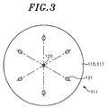
- the insulating plate 116 and the guard electrode 117 have a disk shape, and a circular hole 120 that is a circular through hole is formed at the center thereof (see Fig. 3 ).
- a plurality of (six in this embodiment) oblong holes (through holes) 121 is formed to extend in a diametric direction of the mounting table 111 (the insulating plate 116 and the guard electrode 117) (hereinafter, referred to as "diametric direction").
- the insulating plate 116 and the guard electrode 117 may have at least one oblong hole 121.
- the oblong holes 121 may be provided at regular intervals (60° interval in Fig. 3 ) along the circumferential direction of the mounting table 111 (the insulating plate 116 and the guard electrode 117).
- Fig. 4A is a horizontal cross-sectional view of the circular hole 120 shown in Fig. 3
- Fig. 4B is a vertical cross-sectional view of the vicinity of the circular hole 120 shown in Fig. 3
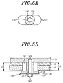
- Fig. 5A is a horizontal cross-sectional view of the oblong hole 121 shown in Fig. 3
- Fig. 5B is a vertical cross-sectional view of the vicinity of the oblong hole 121 shown in Fig. 3 .
- 4B and 5B respectively show that parts of the force electrode 115 corresponding to the circular hole 120 and the oblong hole 121 are non-through holes and the force electrode 115 has screw holes 122, into which respective male screws can be screwed, at inner circumferential surfaces of the non-through holes.
- a cylindrical collar 130 is fitted into the circular hole 120 (fixing part) of Fig. 4A .
- the collar 130 is made of an insulating material, e.g., alumina ceramic, mica-ceramic (Micarex or the like) or the like.
- a flange portion 131 is formed at one end of a cylindrical member of the collar 130.
- a through hole 132, into which a male screw 140 is inserted, is formed along a central axis of the collar 130.
- the force electrode 115, the insulating plate 116 and the guard electrode 117 are sequentially laminated. Then, the collar 130 is inserted into the circular hole 120 from the side of the guard electrode 117, and the male screw 140 is inserted into the through hole 132 of the collar 130 through a washer 133 to be screwed to the screw hole 122.
- a length (L1 in Fig. 4B ) of the collar 130 except the flange portion 131 is set to be smaller than a sum (L2 in Fig. 4B ) of a thickness of the insulating plate 116 and a thickness of the guard electrode 117.
- An outer diameter of the circular hole 120 is preferably set to, e.g., about 1 mm to 20 mm (6 mm in this embodiment).
- an outer diameter of the collar 130 (outer diameter of the part of the collar 130 except the flange portion 131) is preferably set to, e.g., about 1 mm to 20 mm (6 mm in this embodiment).
- a cylindrical collar 135 is fitted into the oblong hole 121 (locking part) formed around the circular hole 120.
- the collar 135 is made of an insulating material, e.g., alumina ceramic, mica-ceramic (Micarex or the like) or the like.
- a flange portion 136 is formed at one end of the collar 135.
- a through hole 137, into which the male screw 140 is inserted, is formed along a central axis of the collar 135.
- the force electrode 115, the insulating plate 116 and the guard electrode 117 are sequentially laminated. Then, the collar 135 is inserted into the oblong hole 121 from the side of the guard electrode 117, and the male screw is inserted into the through hole 137 of the collar 135 through a washer 133 to be screwed to the screw hole 122.
- a length (L3 in Fig. 5B ) of the collar 135 except the flange portion 136 is set to be larger than the sum (L2 in Fig. 5B ) of the thickness of the insulating plate 116 and the thickness of the guard electrode 117.
- the force electrode 115, the insulating plate 116 and the guard electrode 117 are respectively movable in the diametric direction along the oblong hole 121 but are not movable in the circumferential direction.
- the force electrode 115, the insulating plate 116 and the guard electrode 117 are different in their thermal expansion coefficients from each other so that extension/contraction amounts of the the force electrode 115, the insulating plate 116 and the guard electrode 117 in the diametric direction are different from each other, stress is not applied to each of the force electrode 115, the insulating plate 116 and the guard electrode 117.
- a size in a cross-section shape of the oblong hole 121 is preferably set to, e.g., about 1 mm to 20 mm (10 mm in this embodiment) in a longer side, and to, e.g., about 1 mm to 20 mm (6 mm in this embodiment) in a shorter side.
- An outer diameter of the collar 135 is preferably set to, e.g., about 1 mm to 20 mm (6 mm in this embodiment).
- the gap "d" formed between the bottom surface of the guard electrode 117 and the top surface of the flange portion 136 is preferably set to, e.g., about 0.01 mm to 0.5 mm. By doing so, the force electrode 115, the insulating plate 116 and the guard electrode 117 are not pressed by each other in the thickness direction and can be individually moved in the diametric direction.
- the mounting part 114 of the mounting table 111 has a three-layer structure in which the force electrode 115, the insulating plate 116 and the guard electrode 117 are laminated.
- the three plate bodies are fixed at the circular hole 120 provided at the center thereof, and are locked to be movable in the diametric direction at the oblong hole 121 provided at the outer side in the diametric direction.
- the force electrode 115, the insulating plate 116 and the guard electrode 117 are respectively moved in the diametric direction. Therefore, it is possible to suppress the stress due to difference in the extension/contraction amounts, which is caused from difference in the thermal expansion coefficients of the the force electrode 115, the insulating plate 116 and the guard electrode 117.
- the vertical driving mechanism moves the wafer carrier 151 and the load port 152 up and down.
- the optical detector detects a slot in the wafer carrier 151 in which the semiconductor wafer W is accommodated.
- the wafer transfer arm 161 of the wafer transfer mechanism 160 holds the semiconductor wafer W and transfers the semiconductor wafer W to the position alignment mechanism 170.
- the position alignment mechanism 170 detects a notch of the semiconductor wafer W to find a position of the semiconductor wafer W.
- the wafer transfer arm 161 of the wafer transfer mechanism 160 receives the semiconductor wafer W from the position alignment mechanism 170 and mounts the semiconductor wafer W on the mounting table 111 of the measuring unit 110.
- the wafer transfer arm 161 of the wafer transfer mechanism 160 receives the semiconductor wafer W on the mounting table 111 and accommodates the semiconductor wafer W in the wafer carrier 151. Then, the test of the semiconductor wafer W is completed.
Landscapes
- Engineering & Computer Science (AREA)
- Environmental & Geological Engineering (AREA)
- Physics & Mathematics (AREA)
- General Physics & Mathematics (AREA)
- Microelectronics & Electronic Packaging (AREA)
- General Engineering & Computer Science (AREA)
- Computer Hardware Design (AREA)
- Health & Medical Sciences (AREA)
- Toxicology (AREA)
- Testing Or Measuring Of Semiconductors Or The Like (AREA)
- Container, Conveyance, Adherence, Positioning, Of Wafer (AREA)
- Geometry (AREA)
- Measuring Leads Or Probes (AREA)
Abstract
Description
- The present invention relates to a probe device.
- In a manufacturing process of a semiconductor device, a probe device is used to perform an electrical test of a semiconductor device formed on a semiconductor wafer. The probe device drives a mounting table on which the semiconductor wafer is mounted and makes a probe contact with an electrode of the semiconductor device formed on the semiconductor wafer to thereby obtain electrical conduction. The test of the semiconductor device is performed by detecting an output signal from the semiconductor device to which a predetermined test signal has been applied from a measuring device (tester) through the probe.
- A probe device for measuring a minute current and a minute voltage from the semiconductor device employs, as a mounting table on which the semiconductor wafer is mounted, a mounting table including an insulating layer, a first conductive layer fixed to one side of the insulating layer, and a second conductive layer fixed to the other side of the insulating layer (see, e.g.,
Japanese Patent No. 3351956 - However, when the above-mentioned mounting table is used in a wide temperature range (e.g., a temperature range equal to or higher than 300°C), the mounting table may be warped due to difference in thermal expansion coefficients of the insulating layer and the conductive layers, thereby making it difficult to bring the probe into accurate contact with an electrode of the semiconductor device. Further, due to the difference in thermal expansion coefficients of the insulating layer and the conductive layers, the conductive layers may be detached from the insulating layer and thus the mounting table may be damaged. Furthermore, due to the difference in thermal expansion coefficients of the insulating layer and the conductive layers, stress may be applied to the insulating layer to have a crack in the insulating layer and thus the mounting table may be damaged.
- In view of the above, the present invention provides a probe device capable of performing an accurate test without causing warpage or damage of a mounting table.
- In accordance with an aspect, there is provided a probe device for performing an electrical test of a semiconductor device formed on a semiconductor wafer, the probe device including: a mounting table on which the semiconductor wafer is mounted; a driving mechanism configured to bring a probe into contact with an electrode of the semiconductor device mounted on the mounting table; and a temperature control mechanism configured to control a temperature of the mounting table, wherein the mounting table includes a disk-shaped first electrode, a disk-shaped second electrode, and a disk-shaped insulating plate interposed between the first electrode and the second electrode, and wherein the first electrode, the second electrode and the insulating plate are fixed to each other at a fixing part provided at their respective centers, and are locked to be movable in a diametric direction at a locking part provided at an outer side of the fixing part in the diametric direction.
- In accordance with the present invention, an accurate test can be performed without generating a twist and damage in a mounting table.
-
-
Fig. 1 is a plan view schematically showing an entire configuration of a probe device in accordance with an embodiment of the present invention. -
Fig. 2 is a view schematically showing a configuration of a mounting table in the probe device ofFig. 1 . -
Fig. 3 is a plan view schematically showing an insulating plate and a guard electrode ofFig. 2 . -
Fig. 4A is a horizontal cross-sectional view of a circular hole shown inFig. 3 . -
Fig. 4B is a vertical cross-sectional view of the vicinity of the circular hole shown inFig. 3 . -
Fig. 5A is a horizontal cross-sectional view of an oblong hole shown inFig. 3 . -
Fig. 5B is a vertical cross-sectional view of the vicinity of the oblong hole shown inFig. 3 . - Hereinafter, embodiments of the present invention will be described in detail with respect to the accompanying drawings.
-
Fig. 1 is a plan view schematically showing an entire configuration of aprobe device 100 in accordance with an embodiment of the present invention. Theprobe device 100 ofFig. 1 includes ameasuring unit 110 and aloader unit 150 serving as a transfer unit. Themeasuring unit 110 is movable in x-y-z-θ directions, and includes a circular disk-shaped mounting table 111 on which a semiconductor wafer W is mounted. By driving the mounting table 111 by adriving mechanism 112, themeasuring unit 110 makes probes 210 (seeFig. 2 ) provided at a probe card and electrodes of semiconductor devices formed on the semiconductor wafer W contact with each other to measure electrical characteristics of the semiconductor devices. - The
loader unit 150 includes aload port 152 on which a wafer carrier (wafer cassette or FOUP) 151, which accommodates the semiconductor wafer W, is mounted at the front side of the loader unit 150 (lower side inFig. 1 ), and awafer transfer mechanism 160 adjacent to theload port 152. Theloader unit 150 further includes aposition alignment mechanism 170 at the rear side thereof (upper side inFig. 1 ). Theposition alignment mechanism 170 detects a position of a notch of the semiconductor wafer W and an eccentricity state of the semiconductor wafer W by rotating the semiconductor wafer W. - The
wafer transfer mechanism 160 includes awafer transfer arm 161 for vacuum-suctioning and transferring the semiconductor wafer W. Thewafer transfer arm 161 includes a plurality of (two in this embodiment) suction portions (suction pad) 162 for suctioning and holding the semiconductor wafer W. A vacuum line (not shown) connected to a suction source such as a vacuum pump is connected to the attractingportions 162. Thewafer transfer arm 161 may be, if necessary, provided in plural number in a vertically overlapped state. - The
wafer transfer mechanism 160 transfers the semiconductor wafer W between thewafer carrier 151 mounted on theload port 152, theposition alignment mechanism 170, and the mounting table 111 of themeasuring unit 110 by extending, retracting and rotating thewafer transfer arm 161. - The
load port 152 is movable up and down by a vertical driving mechanism (not shown). Asupport frame 153 is provided between theload port 152 and thewafer transfer mechanism 160. Theload port 152 includes an optical detector (not shown). When thewafer carrier 151 mounted on theload port 152 is moved up and down, the optical detector detects presense or absence of the semiconductor wafer W and a slot in thewafer carrier 151 which receives the semiconductor wafer W is accommodated. -
Fig. 2 is a view showing a schematic configuration of the mounting table 111 in theprobe device 100 ofFig. 1 . - The mounting table 111 of
Fig. 2 includes atemperature control mechanism 113 and amounting part 114 at the top of thetemperature control mechanism 113. Thetemperature control mechanism 113 controls a temperature of the semiconductor wafer W mounted on the mounting table 111 in a predetermined temperature range, e.g., in a range of 300°C or above (in this embodiment, a range from -60°C to +400°C). - The
mounting part 114 has a three-layer structure formed of three plate bodies, i.e., aforce electrode 115, aninsulating plate 116, and aguard electrode 117 sequentially laminated from the side of the semiconductor wafer W mounted on themounting part 114. Theinsulating plate 116 is interposed between theforce electrode 115 and theguard electrode 117. The structure of themounting part 114 is not limited to three-layer and may be multi-layer such as four-layer, five-layer or the like. - In the present embodiment, the
force electrode 115 is connected to a force terminal of ameasuring device 200 through acoaxial cable 201. Theguard electrode 117 is connected to a guard terminal of themeasuring device 200 through an outer conductor of thecoaxial cable 201. Aprobe 210 contacting with an electrode of the semiconductor device formed on the semiconductor wafer W is connected to the force terminal of themeasuring device 200 through an inner conductor of acoaxial cable 211, and also connected to the guard terminal of themeasuring device 200 through an outer conductor of thecoaxial cable 211. Although only oneprobe 210 is shown inFig. 2 , a plurality ofprobes 210 may be used. - The
force electrode 115 and theguard electrode 117 are each connected to themeasuring device 200 in the same potential as themeasuring device 200 and in low impedance. Theguard electrode 117 reduces a leaking current flowing through theinsulating plate 116 from theforce electrode 115 and shields electrical noises intruding from the lower side of theguard electrode 117. Therefore, it is possible to accurately measure a minute current and a minute voltage of the semiconductor device formed on the semiconductor wafer W. - As a material of the
force electrode 115 and theguard electrode 117, a conductive metal, e.g., copper, iron, nickel, silver, gold, aluminum, stainless or the like may be used. As a material of theinsulating plate 116, an insulating material, e.g., alumina ceramic, boron nitride, quartz, Teflon™, or the like may be used. - The
insulating plate 116 and theguard electrode 117 have a disk shape, and acircular hole 120 that is a circular through hole is formed at the center thereof (seeFig. 3 ). Around thecircular hole 120, a plurality of (six in this embodiment) oblong holes (through holes) 121 is formed to extend in a diametric direction of the mounting table 111 (theinsulating plate 116 and the guard electrode 117) (hereinafter, referred to as "diametric direction"). Theinsulating plate 116 and theguard electrode 117 may have at least oneoblong hole 121. In a case of having a plurality ofoblong holes 121, as shown inFig. 3 , theoblong holes 121 may be provided at regular intervals (60° interval inFig. 3 ) along the circumferential direction of the mounting table 111 (theinsulating plate 116 and the guard electrode 117). -
Fig. 4A is a horizontal cross-sectional view of thecircular hole 120 shown inFig. 3 , andFig. 4B is a vertical cross-sectional view of the vicinity of thecircular hole 120 shown inFig. 3 .Fig. 5A is a horizontal cross-sectional view of theoblong hole 121 shown inFig. 3 , andFig. 5B is a vertical cross-sectional view of the vicinity of theoblong hole 121 shown inFig. 3 .Figs. 4B and5B respectively show that parts of theforce electrode 115 corresponding to thecircular hole 120 and theoblong hole 121 are non-through holes and theforce electrode 115 has screw holes 122, into which respective male screws can be screwed, at inner circumferential surfaces of the non-through holes. - A
cylindrical collar 130 is fitted into the circular hole 120 (fixing part) ofFig. 4A . Thecollar 130 is made of an insulating material, e.g., alumina ceramic, mica-ceramic (Micarex or the like) or the like. Aflange portion 131 is formed at one end of a cylindrical member of thecollar 130. A throughhole 132, into which amale screw 140 is inserted, is formed along a central axis of thecollar 130. - The
force electrode 115, the insulatingplate 116 and theguard electrode 117 are sequentially laminated. Then, thecollar 130 is inserted into thecircular hole 120 from the side of theguard electrode 117, and themale screw 140 is inserted into the throughhole 132 of thecollar 130 through awasher 133 to be screwed to thescrew hole 122. - A length (L1 in
Fig. 4B ) of thecollar 130 except theflange portion 131 is set to be smaller than a sum (L2 inFig. 4B ) of a thickness of the insulatingplate 116 and a thickness of theguard electrode 117. By doing so, when themale screw 140 is screwed, theguard electrode 117 and the insulatingplate 116 are pressed against theforce electrode 115 by theflange portion 131, and theforce electrode 115, the insulatingplate 116 and theguard electrode 117 are fixed to each other. An outer diameter of thecircular hole 120 is preferably set to, e.g., about 1 mm to 20 mm (6 mm in this embodiment). Further, an outer diameter of the collar 130 (outer diameter of the part of thecollar 130 except the flange portion 131) is preferably set to, e.g., about 1 mm to 20 mm (6 mm in this embodiment). - In
Figs. 5A and 5B , acylindrical collar 135 is fitted into the oblong hole 121 (locking part) formed around thecircular hole 120. Thecollar 135 is made of an insulating material, e.g., alumina ceramic, mica-ceramic (Micarex or the like) or the like. Aflange portion 136 is formed at one end of thecollar 135. A throughhole 137, into which themale screw 140 is inserted, is formed along a central axis of thecollar 135. - The
force electrode 115, the insulatingplate 116 and theguard electrode 117 are sequentially laminated. Then, thecollar 135 is inserted into theoblong hole 121 from the side of theguard electrode 117, and the male screw is inserted into the throughhole 137 of thecollar 135 through awasher 133 to be screwed to thescrew hole 122. - A length (L3 in
Fig. 5B ) of thecollar 135 except theflange portion 136 is set to be larger than the sum (L2 inFig. 5B ) of the thickness of the insulatingplate 116 and the thickness of theguard electrode 117. By doing so, when themale screw 140 is screwed, a gap "d" is formed between a bottom surface of theguard electrode 117 and a top surface of theflange portion 136, so that the insulatingplate 116 and theguard electrode 117 are not fixed to theforce electrode 115 and can be moved in the diametric direction. - That is to say, the
force electrode 115, the insulatingplate 116 and theguard electrode 117 are respectively movable in the diametric direction along theoblong hole 121 but are not movable in the circumferential direction. Accordinlgy, even when theforce electrode 115, the insulatingplate 116 and theguard electrode 117 are different in their thermal expansion coefficients from each other so that extension/contraction amounts of the theforce electrode 115, the insulatingplate 116 and theguard electrode 117 in the diametric direction are different from each other, stress is not applied to each of theforce electrode 115, the insulatingplate 116 and theguard electrode 117. - A size in a cross-section shape of the
oblong hole 121 is preferably set to, e.g., about 1 mm to 20 mm (10 mm in this embodiment) in a longer side, and to, e.g., about 1 mm to 20 mm (6 mm in this embodiment) in a shorter side. An outer diameter of the collar 135 (outer diameter of the part of thecollar 130 except the flange portion 131) is preferably set to, e.g., about 1 mm to 20 mm (6 mm in this embodiment). - The gap "d" formed between the bottom surface of the
guard electrode 117 and the top surface of theflange portion 136 is preferably set to, e.g., about 0.01 mm to 0.5 mm. By doing so, theforce electrode 115, the insulatingplate 116 and theguard electrode 117 are not pressed by each other in the thickness direction and can be individually moved in the diametric direction. - In the probe device having the above configuration, the mounting
part 114 of the mounting table 111 has a three-layer structure in which theforce electrode 115, the insulatingplate 116 and theguard electrode 117 are laminated. However, the three plate bodies are fixed at thecircular hole 120 provided at the center thereof, and are locked to be movable in the diametric direction at theoblong hole 121 provided at the outer side in the diametric direction. - Accordingly, even in a case where a temperature is controlled in a wide temperature range (from -60°C to +400°C in this embodiment) by the
temperature control mechanism 113, theforce electrode 115, the insulatingplate 116 and theguard electrode 117 are respectively moved in the diametric direction. Therefore, it is possible to suppress the stress due to difference in the extension/contraction amounts, which is caused from difference in the thermal expansion coefficients of the theforce electrode 115, the insulatingplate 116 and theguard electrode 117. - Specifically, it is possible to prevent a warpage of the mounting
part 114 which would lead to an inaccurate contact of theprobe 210 with the electrode of the semiconductor device formed on the semiconductor wafer W, so that a test of the semiconductor device can be performed more precisely. Further, it is possible to prevent damage of the mounting table 111 such as detachment of theforce electrode 115 and theguard electrode 117 from the insulatingplate 116, cracks in the insulatingplate 116, and the like. - Next, a test sequence of the semiconductor wafer W by the
probe device 100 having the above configuration will be described. - First, when the
wafer carrier 151 in which the semiconductor wafer W is accommodated is mounted on theload port 152 of theloader unit 150, the vertical driving mechanism moves thewafer carrier 151 and theload port 152 up and down. The optical detector detects a slot in thewafer carrier 151 in which the semiconductor wafer W is accommodated. - The
wafer transfer arm 161 of thewafer transfer mechanism 160 holds the semiconductor wafer W and transfers the semiconductor wafer W to theposition alignment mechanism 170. Theposition alignment mechanism 170 detects a notch of the semiconductor wafer W to find a position of the semiconductor wafer W. - After completing the position detection by the
position alignment mechanism 170, thewafer transfer arm 161 of thewafer transfer mechanism 160 receives the semiconductor wafer W from theposition alignment mechanism 170 and mounts the semiconductor wafer W on the mounting table 111 of the measuringunit 110. - When the
probe 210 is made to contact with the semiconductor device of the semiconductor wafer W on the mounting table 111, an electrical conduction is obtained (seeFig. 2 ). A test signal is supplied to the semiconductor device from the measuring device and an output signal from the semiconductor device is measured to thereby test electrical characteristics of the semiconductor device. - After completing the test on the electrical characteristics of the semiconductor device of the semiconductor wafer W, the
wafer transfer arm 161 of thewafer transfer mechanism 160 receives the semiconductor wafer W on the mounting table 111 and accommodates the semiconductor wafer W in thewafer carrier 151. Then, the test of the semiconductor wafer W is completed. - As described above, the present invention has been described with respect to the above embodiment. However, the present invention is not limited to the above embodiment.
- The present application claims priority based on
Japanese Patent Application No. 2013-065510 filed on March 27, 2013 -
- 100
- probe device
- 110
- measuring unit
- 111
- mounting table
- 150
- loader unit
- 151
- wafer carrier
- 152
- load port
- 153
- support frame
- 160
- wafer transfer mechanism
- 161
- wafer transfer arm
- 162
- suction portion
- 170
- position alignment mechanism
Claims (10)
- A probe device for performing an electrical test of a semiconductor device formed on a semiconductor wafer, the probe device comprising:a mounting table on which the semiconductor wafer is mounted;a driving mechanism configured to bring a probe into contact with an electrode of the semiconductor device mounted on the mounting table; anda temperature control mechanism configured to control a temperature of the mounting table,wherein the mounting table includes a disk-shaped first electrode, a disk-shaped second electrode, and a disk-shaped insulating plate interposed between the first electrode and the second electrode, andwherein the first electrode, the second electrode and the insulating plate are fixed to each other at a fixing part provided at their respective centers, and are locked to be movable in a diametric direction at a locking part provided at an outer side of the fixing part in the diametric direction.
- The probe device of claim 1, wherein the locking part is provided in plural number at intervals along a circumferential direction of the mounting table.
- The probe device of claim 1 or 2, wherein in the locking part, a screw hole is formed in the first electrode and an oblong hole penetrating through the insulating plate and the second electrode in their thickness direction is formed at a position of the insulating plate and the second electrode corresponding to the screw hole, and
wherein the first electrode, the insulating plate and the second electrode are sequentially laminated and a male screw, which is inserted from a side of the second electrode, is screwed to the screw hole. - The probe device of claim 3, wherein a horizontal cross-sectional shape of the oblong hole extends in the diametric direction.
- The probe device of claim 3 or 4, wherein the male screw is made of an insulating material.
- The probe device of any one of claims 3 to 5, wherein in the fixing unit, another screw hole is formed in the first electrode and a circular hole penetrating through the insulating plate and the second electrode in their thickness direction is formed at a position of the insulating plate and the second electrode corresponding to the another screw hole, and
wherein collars each having a cylindrical member and a flange portion at one end of the cylindrical member are respectively fitted into the circular hole of the fixing unit and the oblong hole of the locking unit, and a through hole, into which the male screw is inserted, is formed in each of the collars along a central axis of the cylindrical member. - The probe device of claim 6, wherein in the fixing unit, a length of the collar except the flange portion is set to be smaller than a sum of a thickness of the insulating plate and a thickness of the second electrode.
- The probe device of claim 6, wherein in the locking unit, a length of the collar except the flange portion is set to be larger than a sum of a thickness of the insulating plate and a thickness of the second electrode.
- The probe device of any one of claims 6 to 8, wherein the collars are made of an insulating material.
- The probe device of any one of claims 1 to 9, wherein the first electrode is a force electrode and the second electrode is a guard electrode.
Applications Claiming Priority (2)
| Application Number | Priority Date | Filing Date | Title |
|---|---|---|---|
| JP2013065510A JP6013250B2 (en) | 2013-03-27 | 2013-03-27 | Probe device |
| PCT/JP2014/058149 WO2014157120A1 (en) | 2013-03-27 | 2014-03-18 | Probe device |
Publications (3)
| Publication Number | Publication Date |
|---|---|
| EP2980840A1 true EP2980840A1 (en) | 2016-02-03 |
| EP2980840A4 EP2980840A4 (en) | 2016-12-07 |
| EP2980840B1 EP2980840B1 (en) | 2020-11-04 |
Family
ID=51624092
Family Applications (1)
| Application Number | Title | Priority Date | Filing Date |
|---|---|---|---|
| EP14776367.6A Active EP2980840B1 (en) | 2013-03-27 | 2014-03-18 | Probe device |
Country Status (6)
| Country | Link |
|---|---|
| US (1) | US9739828B2 (en) |
| EP (1) | EP2980840B1 (en) |
| JP (1) | JP6013250B2 (en) |
| KR (1) | KR101800521B1 (en) |
| TW (1) | TWI620942B (en) |
| WO (1) | WO2014157120A1 (en) |
Families Citing this family (3)
| Publication number | Priority date | Publication date | Assignee | Title |
|---|---|---|---|---|
| US11175309B2 (en) | 2014-12-24 | 2021-11-16 | Qualitau, Inc. | Semi-automatic prober |
| CN113053774A (en) * | 2019-12-27 | 2021-06-29 | 迪科特测试科技(苏州)有限公司 | Probe apparatus |
| CN120103120B (en) * | 2025-05-09 | 2025-08-01 | 深圳市森美协尔科技有限公司 | Probe card mounting platform, wafer inspection equipment and design method |
Family Cites Families (13)
| Publication number | Priority date | Publication date | Assignee | Title |
|---|---|---|---|---|
| JPH0762691B2 (en) * | 1987-06-24 | 1995-07-05 | 東京エレクトロン株式会社 | Electrical property measuring device |
| US5610529A (en) | 1995-04-28 | 1997-03-11 | Cascade Microtech, Inc. | Probe station having conductive coating added to thermal chuck insulator |
| US6073681A (en) | 1997-12-31 | 2000-06-13 | Temptronic Corporation | Workpiece chuck |
| JP4490521B2 (en) * | 1999-01-29 | 2010-06-30 | 東京エレクトロン株式会社 | Rotation drive mechanism, mounting mechanism for inspection object, and inspection device |
| EP1356499A2 (en) | 2000-07-10 | 2003-10-29 | Temptronic Corporation | Wafer chuck with interleaved heating and cooling elements |
| JP2002043381A (en) * | 2000-07-19 | 2002-02-08 | Tokyo Electron Ltd | Wafer temperature control device |
| DE10122036B4 (en) * | 2001-05-07 | 2009-12-24 | Karl Suss Dresden Gmbh | Substrate holding device for probes for testing circuit arrangements on disc-shaped substrates |
| JP4686996B2 (en) * | 2004-03-30 | 2011-05-25 | 住友電気工業株式会社 | Heating device |
| JP4433478B2 (en) * | 2005-08-01 | 2010-03-17 | 住友電気工業株式会社 | Heating device and wafer prober equipped with the same |
| US8872532B2 (en) * | 2009-12-31 | 2014-10-28 | Formfactor, Inc. | Wafer test cassette system |
| JP5296117B2 (en) * | 2010-03-12 | 2013-09-25 | 東京エレクトロン株式会社 | Probe device |
| JP5889581B2 (en) * | 2010-09-13 | 2016-03-22 | 東京エレクトロン株式会社 | Wafer inspection equipment |
| JP5605265B2 (en) * | 2011-02-24 | 2014-10-15 | 住友電気工業株式会社 | Heater unit for semiconductor manufacturing equipment |
-
2013
- 2013-03-27 JP JP2013065510A patent/JP6013250B2/en active Active
-
2014
- 2014-03-18 KR KR1020157026492A patent/KR101800521B1/en active Active
- 2014-03-18 US US14/779,870 patent/US9739828B2/en active Active
- 2014-03-18 WO PCT/JP2014/058149 patent/WO2014157120A1/en not_active Ceased
- 2014-03-18 EP EP14776367.6A patent/EP2980840B1/en active Active
- 2014-03-20 TW TW103110462A patent/TWI620942B/en active
Also Published As
| Publication number | Publication date |
|---|---|
| WO2014157120A1 (en) | 2014-10-02 |
| JP6013250B2 (en) | 2016-10-25 |
| US20160047856A1 (en) | 2016-02-18 |
| EP2980840B1 (en) | 2020-11-04 |
| EP2980840A4 (en) | 2016-12-07 |
| US9739828B2 (en) | 2017-08-22 |
| JP2014192285A (en) | 2014-10-06 |
| TWI620942B (en) | 2018-04-11 |
| TW201504643A (en) | 2015-02-01 |
| KR20150135309A (en) | 2015-12-02 |
| KR101800521B1 (en) | 2017-11-22 |
Similar Documents
| Publication | Publication Date | Title |
|---|---|---|
| TW502354B (en) | Inspection device for semiconductor | |
| US20070023320A1 (en) | Wafer holder, heater unit having the wafer holder, and wafer prober having the heater unit | |
| JP6440587B2 (en) | Suction plate, semiconductor device test apparatus, and semiconductor device test method | |
| CN108470690B (en) | detector | |
| US11099227B2 (en) | Multilayer wiring base plate and probe card using the same | |
| KR100810550B1 (en) | Method and apparatus for testing electrical characteristics of object under test | |
| JP2001223247A (en) | Support for conductive contact and contact probe unit | |
| CN105826216B (en) | Semiconductor evaluation device, semiconductor device for inspection, and inspection method of chuck table | |
| US9739828B2 (en) | Probe device | |
| US9759762B2 (en) | Probe device | |
| JPWO2003003027A1 (en) | Support assembly for conductive contacts | |
| JP2007027218A (en) | Wafer holder for wafer prober and wafer prober equipped with the same | |
| EP2980839B1 (en) | Probe device | |
| KR100934507B1 (en) | Mount | |
| US11002760B1 (en) | High isolation housing for testing integrated circuits | |
| US20070024313A1 (en) | Chuck top, wafer holder having the chuck top, and wafer prober having the chuck top | |
| JPH0762691B2 (en) | Electrical property measuring device | |
| JP6680176B2 (en) | Evaluation apparatus and semiconductor chip evaluation method | |
| JPH08111438A (en) | Probe for integrated circuit element | |
| KR100709796B1 (en) | Workpiece loading table | |
| JP6553247B2 (en) | Inspection semiconductor device | |
| CN113225892A (en) | Wiring board and current measuring device | |
| KR20160146043A (en) | Proving chamber | |
| JP2003077967A (en) | Inspection equipment for semiconductor circuits | |
| JP2014013156A (en) | Inspection device |
Legal Events
| Date | Code | Title | Description |
|---|---|---|---|
| PUAI | Public reference made under article 153(3) epc to a published international application that has entered the european phase |
Free format text: ORIGINAL CODE: 0009012 |
|
| 17P | Request for examination filed |
Effective date: 20150924 |
|
| AK | Designated contracting states |
Kind code of ref document: A1 Designated state(s): AL AT BE BG CH CY CZ DE DK EE ES FI FR GB GR HR HU IE IS IT LI LT LU LV MC MK MT NL NO PL PT RO RS SE SI SK SM TR |
|
| AX | Request for extension of the european patent |
Extension state: BA ME |
|
| DAX | Request for extension of the european patent (deleted) | ||
| A4 | Supplementary search report drawn up and despatched |
Effective date: 20161107 |
|
| RIC1 | Information provided on ipc code assigned before grant |
Ipc: H01L 21/66 20060101ALI20161031BHEP Ipc: G01R 31/28 20060101AFI20161031BHEP Ipc: G01R 1/18 20060101ALN20161031BHEP |
|
| GRAP | Despatch of communication of intention to grant a patent |
Free format text: ORIGINAL CODE: EPIDOSNIGR1 |
|
| STAA | Information on the status of an ep patent application or granted ep patent |
Free format text: STATUS: GRANT OF PATENT IS INTENDED |
|
| RIC1 | Information provided on ipc code assigned before grant |
Ipc: G01R 31/28 20060101AFI20200507BHEP Ipc: G01R 1/18 20060101ALN20200507BHEP Ipc: H01L 21/66 20060101ALI20200507BHEP |
|
| INTG | Intention to grant announced |
Effective date: 20200519 |
|
| GRAJ | Information related to disapproval of communication of intention to grant by the applicant or resumption of examination proceedings by the epo deleted |
Free format text: ORIGINAL CODE: EPIDOSDIGR1 |
|
| STAA | Information on the status of an ep patent application or granted ep patent |
Free format text: STATUS: REQUEST FOR EXAMINATION WAS MADE |
|
| REG | Reference to a national code |
Ref country code: DE Ref legal event code: R079 Ref document number: 602014072026 Country of ref document: DE Free format text: PREVIOUS MAIN CLASS: H01L0021660000 Ipc: G01R0031280000 |
|
| GRAR | Information related to intention to grant a patent recorded |
Free format text: ORIGINAL CODE: EPIDOSNIGR71 |
|
| GRAS | Grant fee paid |
Free format text: ORIGINAL CODE: EPIDOSNIGR3 |
|
| STAA | Information on the status of an ep patent application or granted ep patent |
Free format text: STATUS: GRANT OF PATENT IS INTENDED |
|
| GRAA | (expected) grant |
Free format text: ORIGINAL CODE: 0009210 |
|
| STAA | Information on the status of an ep patent application or granted ep patent |
Free format text: STATUS: THE PATENT HAS BEEN GRANTED |
|
| INTC | Intention to grant announced (deleted) | ||
| RIC1 | Information provided on ipc code assigned before grant |
Ipc: G01R 31/28 20060101AFI20200917BHEP Ipc: G01R 1/18 20060101ALN20200917BHEP Ipc: H01L 21/66 20060101ALI20200917BHEP |
|
| AK | Designated contracting states |
Kind code of ref document: B1 Designated state(s): AL AT BE BG CH CY CZ DE DK EE ES FI FR GB GR HR HU IE IS IT LI LT LU LV MC MK MT NL NO PL PT RO RS SE SI SK SM TR |
|
| INTG | Intention to grant announced |
Effective date: 20200929 |
|
| REG | Reference to a national code |
Ref country code: GB Ref legal event code: FG4D |
|
| REG | Reference to a national code |
Ref country code: CH Ref legal event code: EP |
|
| REG | Reference to a national code |
Ref country code: AT Ref legal event code: REF Ref document number: 1331509 Country of ref document: AT Kind code of ref document: T Effective date: 20201115 |
|
| REG | Reference to a national code |
Ref country code: IE Ref legal event code: FG4D |
|
| REG | Reference to a national code |
Ref country code: DE Ref legal event code: R096 Ref document number: 602014072026 Country of ref document: DE |
|
| REG | Reference to a national code |
Ref country code: NL Ref legal event code: MP Effective date: 20201104 |
|
| REG | Reference to a national code |
Ref country code: AT Ref legal event code: MK05 Ref document number: 1331509 Country of ref document: AT Kind code of ref document: T Effective date: 20201104 |
|
| PG25 | Lapsed in a contracting state [announced via postgrant information from national office to epo] |
Ref country code: NO Free format text: LAPSE BECAUSE OF FAILURE TO SUBMIT A TRANSLATION OF THE DESCRIPTION OR TO PAY THE FEE WITHIN THE PRESCRIBED TIME-LIMIT Effective date: 20210204 Ref country code: PT Free format text: LAPSE BECAUSE OF FAILURE TO SUBMIT A TRANSLATION OF THE DESCRIPTION OR TO PAY THE FEE WITHIN THE PRESCRIBED TIME-LIMIT Effective date: 20210304 Ref country code: FI Free format text: LAPSE BECAUSE OF FAILURE TO SUBMIT A TRANSLATION OF THE DESCRIPTION OR TO PAY THE FEE WITHIN THE PRESCRIBED TIME-LIMIT Effective date: 20201104 Ref country code: RS Free format text: LAPSE BECAUSE OF FAILURE TO SUBMIT A TRANSLATION OF THE DESCRIPTION OR TO PAY THE FEE WITHIN THE PRESCRIBED TIME-LIMIT Effective date: 20201104 Ref country code: GR Free format text: LAPSE BECAUSE OF FAILURE TO SUBMIT A TRANSLATION OF THE DESCRIPTION OR TO PAY THE FEE WITHIN THE PRESCRIBED TIME-LIMIT Effective date: 20210205 |
|
| PG25 | Lapsed in a contracting state [announced via postgrant information from national office to epo] |
Ref country code: IS Free format text: LAPSE BECAUSE OF FAILURE TO SUBMIT A TRANSLATION OF THE DESCRIPTION OR TO PAY THE FEE WITHIN THE PRESCRIBED TIME-LIMIT Effective date: 20210304 Ref country code: SE Free format text: LAPSE BECAUSE OF FAILURE TO SUBMIT A TRANSLATION OF THE DESCRIPTION OR TO PAY THE FEE WITHIN THE PRESCRIBED TIME-LIMIT Effective date: 20201104 Ref country code: LV Free format text: LAPSE BECAUSE OF FAILURE TO SUBMIT A TRANSLATION OF THE DESCRIPTION OR TO PAY THE FEE WITHIN THE PRESCRIBED TIME-LIMIT Effective date: 20201104 Ref country code: PL Free format text: LAPSE BECAUSE OF FAILURE TO SUBMIT A TRANSLATION OF THE DESCRIPTION OR TO PAY THE FEE WITHIN THE PRESCRIBED TIME-LIMIT Effective date: 20201104 Ref country code: AT Free format text: LAPSE BECAUSE OF FAILURE TO SUBMIT A TRANSLATION OF THE DESCRIPTION OR TO PAY THE FEE WITHIN THE PRESCRIBED TIME-LIMIT Effective date: 20201104 Ref country code: ES Free format text: LAPSE BECAUSE OF FAILURE TO SUBMIT A TRANSLATION OF THE DESCRIPTION OR TO PAY THE FEE WITHIN THE PRESCRIBED TIME-LIMIT Effective date: 20201104 Ref country code: BG Free format text: LAPSE BECAUSE OF FAILURE TO SUBMIT A TRANSLATION OF THE DESCRIPTION OR TO PAY THE FEE WITHIN THE PRESCRIBED TIME-LIMIT Effective date: 20210204 |
|
| REG | Reference to a national code |
Ref country code: LT Ref legal event code: MG9D |
|
| PG25 | Lapsed in a contracting state [announced via postgrant information from national office to epo] |
Ref country code: HR Free format text: LAPSE BECAUSE OF FAILURE TO SUBMIT A TRANSLATION OF THE DESCRIPTION OR TO PAY THE FEE WITHIN THE PRESCRIBED TIME-LIMIT Effective date: 20201104 |
|
| PG25 | Lapsed in a contracting state [announced via postgrant information from national office to epo] |
Ref country code: LT Free format text: LAPSE BECAUSE OF FAILURE TO SUBMIT A TRANSLATION OF THE DESCRIPTION OR TO PAY THE FEE WITHIN THE PRESCRIBED TIME-LIMIT Effective date: 20201104 Ref country code: RO Free format text: LAPSE BECAUSE OF FAILURE TO SUBMIT A TRANSLATION OF THE DESCRIPTION OR TO PAY THE FEE WITHIN THE PRESCRIBED TIME-LIMIT Effective date: 20201104 Ref country code: SK Free format text: LAPSE BECAUSE OF FAILURE TO SUBMIT A TRANSLATION OF THE DESCRIPTION OR TO PAY THE FEE WITHIN THE PRESCRIBED TIME-LIMIT Effective date: 20201104 Ref country code: SM Free format text: LAPSE BECAUSE OF FAILURE TO SUBMIT A TRANSLATION OF THE DESCRIPTION OR TO PAY THE FEE WITHIN THE PRESCRIBED TIME-LIMIT Effective date: 20201104 Ref country code: CZ Free format text: LAPSE BECAUSE OF FAILURE TO SUBMIT A TRANSLATION OF THE DESCRIPTION OR TO PAY THE FEE WITHIN THE PRESCRIBED TIME-LIMIT Effective date: 20201104 Ref country code: EE Free format text: LAPSE BECAUSE OF FAILURE TO SUBMIT A TRANSLATION OF THE DESCRIPTION OR TO PAY THE FEE WITHIN THE PRESCRIBED TIME-LIMIT Effective date: 20201104 |
|
| REG | Reference to a national code |
Ref country code: DE Ref legal event code: R097 Ref document number: 602014072026 Country of ref document: DE |
|
| PG25 | Lapsed in a contracting state [announced via postgrant information from national office to epo] |
Ref country code: DK Free format text: LAPSE BECAUSE OF FAILURE TO SUBMIT A TRANSLATION OF THE DESCRIPTION OR TO PAY THE FEE WITHIN THE PRESCRIBED TIME-LIMIT Effective date: 20201104 |
|
| PLBE | No opposition filed within time limit |
Free format text: ORIGINAL CODE: 0009261 |
|
| STAA | Information on the status of an ep patent application or granted ep patent |
Free format text: STATUS: NO OPPOSITION FILED WITHIN TIME LIMIT |
|
| 26N | No opposition filed |
Effective date: 20210805 |
|
| PG25 | Lapsed in a contracting state [announced via postgrant information from national office to epo] |
Ref country code: MC Free format text: LAPSE BECAUSE OF FAILURE TO SUBMIT A TRANSLATION OF THE DESCRIPTION OR TO PAY THE FEE WITHIN THE PRESCRIBED TIME-LIMIT Effective date: 20201104 Ref country code: NL Free format text: LAPSE BECAUSE OF FAILURE TO SUBMIT A TRANSLATION OF THE DESCRIPTION OR TO PAY THE FEE WITHIN THE PRESCRIBED TIME-LIMIT Effective date: 20201104 Ref country code: AL Free format text: LAPSE BECAUSE OF FAILURE TO SUBMIT A TRANSLATION OF THE DESCRIPTION OR TO PAY THE FEE WITHIN THE PRESCRIBED TIME-LIMIT Effective date: 20201104 Ref country code: IT Free format text: LAPSE BECAUSE OF FAILURE TO SUBMIT A TRANSLATION OF THE DESCRIPTION OR TO PAY THE FEE WITHIN THE PRESCRIBED TIME-LIMIT Effective date: 20201104 |
|
| REG | Reference to a national code |
Ref country code: CH Ref legal event code: PL |
|
| GBPC | Gb: european patent ceased through non-payment of renewal fee |
Effective date: 20210318 |
|
| PG25 | Lapsed in a contracting state [announced via postgrant information from national office to epo] |
Ref country code: SI Free format text: LAPSE BECAUSE OF FAILURE TO SUBMIT A TRANSLATION OF THE DESCRIPTION OR TO PAY THE FEE WITHIN THE PRESCRIBED TIME-LIMIT Effective date: 20201104 |
|
| REG | Reference to a national code |
Ref country code: BE Ref legal event code: MM Effective date: 20210331 |
|
| PG25 | Lapsed in a contracting state [announced via postgrant information from national office to epo] |
Ref country code: LI Free format text: LAPSE BECAUSE OF NON-PAYMENT OF DUE FEES Effective date: 20210331 Ref country code: LU Free format text: LAPSE BECAUSE OF NON-PAYMENT OF DUE FEES Effective date: 20210318 Ref country code: CH Free format text: LAPSE BECAUSE OF NON-PAYMENT OF DUE FEES Effective date: 20210331 Ref country code: FR Free format text: LAPSE BECAUSE OF NON-PAYMENT OF DUE FEES Effective date: 20210331 Ref country code: IE Free format text: LAPSE BECAUSE OF NON-PAYMENT OF DUE FEES Effective date: 20210318 Ref country code: GB Free format text: LAPSE BECAUSE OF NON-PAYMENT OF DUE FEES Effective date: 20210318 |
|
| PG25 | Lapsed in a contracting state [announced via postgrant information from national office to epo] |
Ref country code: IS Free format text: LAPSE BECAUSE OF FAILURE TO SUBMIT A TRANSLATION OF THE DESCRIPTION OR TO PAY THE FEE WITHIN THE PRESCRIBED TIME-LIMIT Effective date: 20210304 |
|
| PG25 | Lapsed in a contracting state [announced via postgrant information from national office to epo] |
Ref country code: BE Free format text: LAPSE BECAUSE OF NON-PAYMENT OF DUE FEES Effective date: 20210331 |
|
| PG25 | Lapsed in a contracting state [announced via postgrant information from national office to epo] |
Ref country code: HU Free format text: LAPSE BECAUSE OF FAILURE TO SUBMIT A TRANSLATION OF THE DESCRIPTION OR TO PAY THE FEE WITHIN THE PRESCRIBED TIME-LIMIT; INVALID AB INITIO Effective date: 20140318 |
|
| PG25 | Lapsed in a contracting state [announced via postgrant information from national office to epo] |
Ref country code: CY Free format text: LAPSE BECAUSE OF FAILURE TO SUBMIT A TRANSLATION OF THE DESCRIPTION OR TO PAY THE FEE WITHIN THE PRESCRIBED TIME-LIMIT Effective date: 20201104 |
|
| PG25 | Lapsed in a contracting state [announced via postgrant information from national office to epo] |
Ref country code: MK Free format text: LAPSE BECAUSE OF FAILURE TO SUBMIT A TRANSLATION OF THE DESCRIPTION OR TO PAY THE FEE WITHIN THE PRESCRIBED TIME-LIMIT Effective date: 20201104 |
|
| PG25 | Lapsed in a contracting state [announced via postgrant information from national office to epo] |
Ref country code: MT Free format text: LAPSE BECAUSE OF FAILURE TO SUBMIT A TRANSLATION OF THE DESCRIPTION OR TO PAY THE FEE WITHIN THE PRESCRIBED TIME-LIMIT Effective date: 20201104 |
|
| PG25 | Lapsed in a contracting state [announced via postgrant information from national office to epo] |
Ref country code: TR Free format text: LAPSE BECAUSE OF FAILURE TO SUBMIT A TRANSLATION OF THE DESCRIPTION OR TO PAY THE FEE WITHIN THE PRESCRIBED TIME-LIMIT Effective date: 20201104 |
|
| PGFP | Annual fee paid to national office [announced via postgrant information from national office to epo] |
Ref country code: DE Payment date: 20260128 Year of fee payment: 13 |