EP2980829B1 - Plasma processing apparatus and plasma processing method - Google Patents
Plasma processing apparatus and plasma processing method Download PDFInfo
- Publication number
- EP2980829B1 EP2980829B1 EP15178628.2A EP15178628A EP2980829B1 EP 2980829 B1 EP2980829 B1 EP 2980829B1 EP 15178628 A EP15178628 A EP 15178628A EP 2980829 B1 EP2980829 B1 EP 2980829B1
- Authority
- EP
- European Patent Office
- Prior art keywords
- electrode
- frequency power
- film
- plasma processing
- chamber
- Prior art date
- Legal status (The legal status is an assumption and is not a legal conclusion. Google has not performed a legal analysis and makes no representation as to the accuracy of the status listed.)
- Not-in-force
Links
Images
Classifications
-
- C—CHEMISTRY; METALLURGY
- C23—COATING METALLIC MATERIAL; COATING MATERIAL WITH METALLIC MATERIAL; CHEMICAL SURFACE TREATMENT; DIFFUSION TREATMENT OF METALLIC MATERIAL; COATING BY VACUUM EVAPORATION, BY SPUTTERING, BY ION IMPLANTATION OR BY CHEMICAL VAPOUR DEPOSITION, IN GENERAL; INHIBITING CORROSION OF METALLIC MATERIAL OR INCRUSTATION IN GENERAL
- C23C—COATING METALLIC MATERIAL; COATING MATERIAL WITH METALLIC MATERIAL; SURFACE TREATMENT OF METALLIC MATERIAL BY DIFFUSION INTO THE SURFACE, BY CHEMICAL CONVERSION OR SUBSTITUTION; COATING BY VACUUM EVAPORATION, BY SPUTTERING, BY ION IMPLANTATION OR BY CHEMICAL VAPOUR DEPOSITION, IN GENERAL
- C23C14/00—Coating by vacuum evaporation, by sputtering or by ion implantation of the coating forming material
- C23C14/22—Coating by vacuum evaporation, by sputtering or by ion implantation of the coating forming material characterised by the process of coating
- C23C14/34—Sputtering
-
- C—CHEMISTRY; METALLURGY
- C23—COATING METALLIC MATERIAL; COATING MATERIAL WITH METALLIC MATERIAL; CHEMICAL SURFACE TREATMENT; DIFFUSION TREATMENT OF METALLIC MATERIAL; COATING BY VACUUM EVAPORATION, BY SPUTTERING, BY ION IMPLANTATION OR BY CHEMICAL VAPOUR DEPOSITION, IN GENERAL; INHIBITING CORROSION OF METALLIC MATERIAL OR INCRUSTATION IN GENERAL
- C23C—COATING METALLIC MATERIAL; COATING MATERIAL WITH METALLIC MATERIAL; SURFACE TREATMENT OF METALLIC MATERIAL BY DIFFUSION INTO THE SURFACE, BY CHEMICAL CONVERSION OR SUBSTITUTION; COATING BY VACUUM EVAPORATION, BY SPUTTERING, BY ION IMPLANTATION OR BY CHEMICAL VAPOUR DEPOSITION, IN GENERAL
- C23C14/00—Coating by vacuum evaporation, by sputtering or by ion implantation of the coating forming material
- C23C14/0021—Reactive sputtering or evaporation
- C23C14/0036—Reactive sputtering
-
- C—CHEMISTRY; METALLURGY
- C23—COATING METALLIC MATERIAL; COATING MATERIAL WITH METALLIC MATERIAL; CHEMICAL SURFACE TREATMENT; DIFFUSION TREATMENT OF METALLIC MATERIAL; COATING BY VACUUM EVAPORATION, BY SPUTTERING, BY ION IMPLANTATION OR BY CHEMICAL VAPOUR DEPOSITION, IN GENERAL; INHIBITING CORROSION OF METALLIC MATERIAL OR INCRUSTATION IN GENERAL
- C23C—COATING METALLIC MATERIAL; COATING MATERIAL WITH METALLIC MATERIAL; SURFACE TREATMENT OF METALLIC MATERIAL BY DIFFUSION INTO THE SURFACE, BY CHEMICAL CONVERSION OR SUBSTITUTION; COATING BY VACUUM EVAPORATION, BY SPUTTERING, BY ION IMPLANTATION OR BY CHEMICAL VAPOUR DEPOSITION, IN GENERAL
- C23C14/00—Coating by vacuum evaporation, by sputtering or by ion implantation of the coating forming material
- C23C14/06—Coating by vacuum evaporation, by sputtering or by ion implantation of the coating forming material characterised by the coating material
- C23C14/0605—Carbon
-
- C—CHEMISTRY; METALLURGY
- C23—COATING METALLIC MATERIAL; COATING MATERIAL WITH METALLIC MATERIAL; CHEMICAL SURFACE TREATMENT; DIFFUSION TREATMENT OF METALLIC MATERIAL; COATING BY VACUUM EVAPORATION, BY SPUTTERING, BY ION IMPLANTATION OR BY CHEMICAL VAPOUR DEPOSITION, IN GENERAL; INHIBITING CORROSION OF METALLIC MATERIAL OR INCRUSTATION IN GENERAL
- C23C—COATING METALLIC MATERIAL; COATING MATERIAL WITH METALLIC MATERIAL; SURFACE TREATMENT OF METALLIC MATERIAL BY DIFFUSION INTO THE SURFACE, BY CHEMICAL CONVERSION OR SUBSTITUTION; COATING BY VACUUM EVAPORATION, BY SPUTTERING, BY ION IMPLANTATION OR BY CHEMICAL VAPOUR DEPOSITION, IN GENERAL
- C23C14/00—Coating by vacuum evaporation, by sputtering or by ion implantation of the coating forming material
- C23C14/06—Coating by vacuum evaporation, by sputtering or by ion implantation of the coating forming material characterised by the coating material
- C23C14/0694—Halides
-
- C—CHEMISTRY; METALLURGY
- C23—COATING METALLIC MATERIAL; COATING MATERIAL WITH METALLIC MATERIAL; CHEMICAL SURFACE TREATMENT; DIFFUSION TREATMENT OF METALLIC MATERIAL; COATING BY VACUUM EVAPORATION, BY SPUTTERING, BY ION IMPLANTATION OR BY CHEMICAL VAPOUR DEPOSITION, IN GENERAL; INHIBITING CORROSION OF METALLIC MATERIAL OR INCRUSTATION IN GENERAL
- C23C—COATING METALLIC MATERIAL; COATING MATERIAL WITH METALLIC MATERIAL; SURFACE TREATMENT OF METALLIC MATERIAL BY DIFFUSION INTO THE SURFACE, BY CHEMICAL CONVERSION OR SUBSTITUTION; COATING BY VACUUM EVAPORATION, BY SPUTTERING, BY ION IMPLANTATION OR BY CHEMICAL VAPOUR DEPOSITION, IN GENERAL
- C23C14/00—Coating by vacuum evaporation, by sputtering or by ion implantation of the coating forming material
- C23C14/22—Coating by vacuum evaporation, by sputtering or by ion implantation of the coating forming material characterised by the process of coating
- C23C14/34—Sputtering
- C23C14/3407—Cathode assembly for sputtering apparatus, e.g. Target
- C23C14/3414—Metallurgical or chemical aspects of target preparation, e.g. casting, powder metallurgy
-
- C—CHEMISTRY; METALLURGY
- C23—COATING METALLIC MATERIAL; COATING MATERIAL WITH METALLIC MATERIAL; CHEMICAL SURFACE TREATMENT; DIFFUSION TREATMENT OF METALLIC MATERIAL; COATING BY VACUUM EVAPORATION, BY SPUTTERING, BY ION IMPLANTATION OR BY CHEMICAL VAPOUR DEPOSITION, IN GENERAL; INHIBITING CORROSION OF METALLIC MATERIAL OR INCRUSTATION IN GENERAL
- C23C—COATING METALLIC MATERIAL; COATING MATERIAL WITH METALLIC MATERIAL; SURFACE TREATMENT OF METALLIC MATERIAL BY DIFFUSION INTO THE SURFACE, BY CHEMICAL CONVERSION OR SUBSTITUTION; COATING BY VACUUM EVAPORATION, BY SPUTTERING, BY ION IMPLANTATION OR BY CHEMICAL VAPOUR DEPOSITION, IN GENERAL
- C23C14/00—Coating by vacuum evaporation, by sputtering or by ion implantation of the coating forming material
- C23C14/22—Coating by vacuum evaporation, by sputtering or by ion implantation of the coating forming material characterised by the process of coating
- C23C14/34—Sputtering
- C23C14/3435—Applying energy to the substrate during sputtering
- C23C14/345—Applying energy to the substrate during sputtering using substrate bias
-
- C—CHEMISTRY; METALLURGY
- C23—COATING METALLIC MATERIAL; COATING MATERIAL WITH METALLIC MATERIAL; CHEMICAL SURFACE TREATMENT; DIFFUSION TREATMENT OF METALLIC MATERIAL; COATING BY VACUUM EVAPORATION, BY SPUTTERING, BY ION IMPLANTATION OR BY CHEMICAL VAPOUR DEPOSITION, IN GENERAL; INHIBITING CORROSION OF METALLIC MATERIAL OR INCRUSTATION IN GENERAL
- C23C—COATING METALLIC MATERIAL; COATING MATERIAL WITH METALLIC MATERIAL; SURFACE TREATMENT OF METALLIC MATERIAL BY DIFFUSION INTO THE SURFACE, BY CHEMICAL CONVERSION OR SUBSTITUTION; COATING BY VACUUM EVAPORATION, BY SPUTTERING, BY ION IMPLANTATION OR BY CHEMICAL VAPOUR DEPOSITION, IN GENERAL
- C23C16/00—Chemical coating by decomposition of gaseous compounds, without leaving reaction products of surface material in the coating, i.e. chemical vapour deposition [CVD] processes
- C23C16/22—Chemical coating by decomposition of gaseous compounds, without leaving reaction products of surface material in the coating, i.e. chemical vapour deposition [CVD] processes characterised by the deposition of inorganic material, other than metallic material
- C23C16/30—Deposition of compounds, mixtures or solid solutions, e.g. borides, carbides, nitrides
-
- C—CHEMISTRY; METALLURGY
- C23—COATING METALLIC MATERIAL; COATING MATERIAL WITH METALLIC MATERIAL; CHEMICAL SURFACE TREATMENT; DIFFUSION TREATMENT OF METALLIC MATERIAL; COATING BY VACUUM EVAPORATION, BY SPUTTERING, BY ION IMPLANTATION OR BY CHEMICAL VAPOUR DEPOSITION, IN GENERAL; INHIBITING CORROSION OF METALLIC MATERIAL OR INCRUSTATION IN GENERAL
- C23C—COATING METALLIC MATERIAL; COATING MATERIAL WITH METALLIC MATERIAL; SURFACE TREATMENT OF METALLIC MATERIAL BY DIFFUSION INTO THE SURFACE, BY CHEMICAL CONVERSION OR SUBSTITUTION; COATING BY VACUUM EVAPORATION, BY SPUTTERING, BY ION IMPLANTATION OR BY CHEMICAL VAPOUR DEPOSITION, IN GENERAL
- C23C16/00—Chemical coating by decomposition of gaseous compounds, without leaving reaction products of surface material in the coating, i.e. chemical vapour deposition [CVD] processes
- C23C16/44—Chemical coating by decomposition of gaseous compounds, without leaving reaction products of surface material in the coating, i.e. chemical vapour deposition [CVD] processes characterised by the method of coating
- C23C16/448—Chemical coating by decomposition of gaseous compounds, without leaving reaction products of surface material in the coating, i.e. chemical vapour deposition [CVD] processes characterised by the method of coating characterised by the method used for generating reactive gas streams, e.g. by evaporation or sublimation of precursor materials
-
- C—CHEMISTRY; METALLURGY
- C23—COATING METALLIC MATERIAL; COATING MATERIAL WITH METALLIC MATERIAL; CHEMICAL SURFACE TREATMENT; DIFFUSION TREATMENT OF METALLIC MATERIAL; COATING BY VACUUM EVAPORATION, BY SPUTTERING, BY ION IMPLANTATION OR BY CHEMICAL VAPOUR DEPOSITION, IN GENERAL; INHIBITING CORROSION OF METALLIC MATERIAL OR INCRUSTATION IN GENERAL
- C23C—COATING METALLIC MATERIAL; COATING MATERIAL WITH METALLIC MATERIAL; SURFACE TREATMENT OF METALLIC MATERIAL BY DIFFUSION INTO THE SURFACE, BY CHEMICAL CONVERSION OR SUBSTITUTION; COATING BY VACUUM EVAPORATION, BY SPUTTERING, BY ION IMPLANTATION OR BY CHEMICAL VAPOUR DEPOSITION, IN GENERAL
- C23C16/00—Chemical coating by decomposition of gaseous compounds, without leaving reaction products of surface material in the coating, i.e. chemical vapour deposition [CVD] processes
- C23C16/44—Chemical coating by decomposition of gaseous compounds, without leaving reaction products of surface material in the coating, i.e. chemical vapour deposition [CVD] processes characterised by the method of coating
- C23C16/50—Chemical coating by decomposition of gaseous compounds, without leaving reaction products of surface material in the coating, i.e. chemical vapour deposition [CVD] processes characterised by the method of coating using electric discharges
- C23C16/505—Chemical coating by decomposition of gaseous compounds, without leaving reaction products of surface material in the coating, i.e. chemical vapour deposition [CVD] processes characterised by the method of coating using electric discharges using radio frequency discharges
- C23C16/509—Chemical coating by decomposition of gaseous compounds, without leaving reaction products of surface material in the coating, i.e. chemical vapour deposition [CVD] processes characterised by the method of coating using electric discharges using radio frequency discharges using internal electrodes
-
- H—ELECTRICITY
- H01—ELECTRIC ELEMENTS
- H01J—ELECTRIC DISCHARGE TUBES OR DISCHARGE LAMPS
- H01J37/00—Discharge tubes with provision for introducing objects or material to be exposed to the discharge, e.g. for the purpose of examination or processing thereof
- H01J37/32—Gas-filled discharge tubes
- H01J37/32431—Constructional details of the reactor
- H01J37/32532—Electrodes
- H01J37/32568—Relative arrangement or disposition of electrodes; moving means
-
- H—ELECTRICITY
- H01—ELECTRIC ELEMENTS
- H01J—ELECTRIC DISCHARGE TUBES OR DISCHARGE LAMPS
- H01J37/00—Discharge tubes with provision for introducing objects or material to be exposed to the discharge, e.g. for the purpose of examination or processing thereof
- H01J37/32—Gas-filled discharge tubes
- H01J37/32431—Constructional details of the reactor
- H01J37/32532—Electrodes
- H01J37/32577—Electrical connecting means
-
- H—ELECTRICITY
- H01—ELECTRIC ELEMENTS
- H01J—ELECTRIC DISCHARGE TUBES OR DISCHARGE LAMPS
- H01J37/00—Discharge tubes with provision for introducing objects or material to be exposed to the discharge, e.g. for the purpose of examination or processing thereof
- H01J37/32—Gas-filled discharge tubes
- H01J37/34—Gas-filled discharge tubes operating with cathodic sputtering
- H01J37/3411—Constructional aspects of the reactor
- H01J37/3414—Targets
- H01J37/3417—Arrangements
-
- H—ELECTRICITY
- H01—ELECTRIC ELEMENTS
- H01J—ELECTRIC DISCHARGE TUBES OR DISCHARGE LAMPS
- H01J37/00—Discharge tubes with provision for introducing objects or material to be exposed to the discharge, e.g. for the purpose of examination or processing thereof
- H01J37/32—Gas-filled discharge tubes
- H01J37/34—Gas-filled discharge tubes operating with cathodic sputtering
- H01J37/3411—Constructional aspects of the reactor
- H01J37/3414—Targets
- H01J37/3426—Material
-
- H—ELECTRICITY
- H01—ELECTRIC ELEMENTS
- H01J—ELECTRIC DISCHARGE TUBES OR DISCHARGE LAMPS
- H01J37/00—Discharge tubes with provision for introducing objects or material to be exposed to the discharge, e.g. for the purpose of examination or processing thereof
- H01J37/32—Gas-filled discharge tubes
- H01J37/34—Gas-filled discharge tubes operating with cathodic sputtering
- H01J37/3411—Constructional aspects of the reactor
- H01J37/3414—Targets
- H01J37/3432—Target-material dispenser
-
- H—ELECTRICITY
- H01—ELECTRIC ELEMENTS
- H01J—ELECTRIC DISCHARGE TUBES OR DISCHARGE LAMPS
- H01J37/00—Discharge tubes with provision for introducing objects or material to be exposed to the discharge, e.g. for the purpose of examination or processing thereof
- H01J37/32—Gas-filled discharge tubes
- H01J37/34—Gas-filled discharge tubes operating with cathodic sputtering
- H01J37/3411—Constructional aspects of the reactor
- H01J37/3438—Electrodes other than cathode
-
- H—ELECTRICITY
- H01—ELECTRIC ELEMENTS
- H01J—ELECTRIC DISCHARGE TUBES OR DISCHARGE LAMPS
- H01J37/00—Discharge tubes with provision for introducing objects or material to be exposed to the discharge, e.g. for the purpose of examination or processing thereof
- H01J37/32—Gas-filled discharge tubes
- H01J37/34—Gas-filled discharge tubes operating with cathodic sputtering
- H01J37/3488—Constructional details of particle beam apparatus not otherwise provided for, e.g. arrangement, mounting, housing, environment; special provisions for cleaning or maintenance of the apparatus
- H01J37/3491—Manufacturing of targets
Definitions
- An aspect of this disclosure relates to a plasma processing apparatus and a plasma processing method.
- Japanese Laid-Open Patent 15 Publications No. 2009-280916 and No. 2004-2 66112 discloses a sputter deposition method where a film is formed on an inner wall of, for example, a contact hole, a through hole, or a wiring groove by 20 applying pulsed direct-current power to a target material.
- a method of processing a substrate includes applying RF power at VHF frequency to a target comprising metal disposed in the PVD chamber above the substrate to form a plasma from a plasma-forming gas, sputtering metal atoms from the target using the plasma while maintaining a first pressure in the PVD chamber sufficient to ionize a predominant portion of the sputtered metal atoms, depositing the ionized metal atoms on a bottom surface of the opening and on a first surface of the substrate, applying a first RF power to redistribute at least some of the deposited metal atoms from the bottom surface and upper surface to sidewalls of the opening, and repeating the deposition the redistribution processes until a first layer of metal is deposited on substantially all surfaces of the opening.
- US 2005/023130 A1 discloses a reactive sputtering apparatus, wherein an inert-gas supplying hole is provided in a movable target unit whose one end is open and whose conductance is controlled, and a reactive gas containing at least fluorine or oxygen can be supplied to a space between the target and a substrate.
- the apparatus is constructed so as to emit the reactive gas toward the substrate.
- a reactive-gas emitting location is in the space between the target and the substrate such that a concentration of the reactive gas on the substrate surface can be maintained at a higher level.
- a reactive-gas emitting port is moved or the reactive-gas emitting location is changed.
- the concentration of the reactive gas on the substrate surface can be effectively kept constant, and a high-quality optical thin film can be formed.
- a plasma processing apparatus is alternatively defined by the combination of features of claim 1 or claim 5.
- Dependent claims relate to preferred embodiments.
- a method according to the present invention is alternatively defined by the combination of features of claims 6 or of claim 7. The dependent claim relates to preferred embodiments.
- a plasma processing apparatus that includes a first electrode on which a substrate is placeable, a second electrode that is disposed to face the first electrode across a predetermined gap, a chamber that houses the first electrode and the second electrode, a first high-frequency power supply that supplies first high-frequency power to the second electrode, a direct- current power supply that supplies direct-current power to the second electrode, and a gas supply source.
- the plasma processing apparatus is configured to generate first plasma to form a film of a reaction product on the second electrode by causing the first high-frequency power supply to supply the first high-frequency power to the second electrode and causing the gas supply source to supply a first gas into the chamber; and generate second plasma to sputter the film of the reaction product on the second electrode by causing the first high-frequency power supply to supply the first high-frequency power to the second electrode, causing the direct-current power supply to supply the direct-current power to the second electrode, and causing the gas supply source to supply a second gas into the chamber.
- a film e.g., a film including carbon (C) and fluorine (F)
- a film including carbon (C) and fluorine (F) for which no target material suitable to be placed beforehand in a chamber is available.
- An aspect of this disclosure provides a plasma processing apparatus and a plasma processing method that can form, by sputter deposition, a film for which no target material suitable to be placed beforehand in a chamber is available.
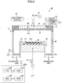
- the plasma processing apparatus 10 includes a cylindrical chamber 12 comprised of a metal such as aluminum or stainless steel.
- the chamber 12 is grounded.
- An opening is formed at the upper end of the chamber 12.
- An upper electrode 15 is disposed at the opening via an insulator 14.
- the insulator 14 and the upper electrode 15 constitute a lid for closing the opening of the chamber 12.
- the mount table 20 is comprised of, for example, aluminum and is supported via an insulating holder (not shown) by the chamber 12.
- An electrostatic chuck 22 for holding the wafer W is provided on an upper surface of the mount table 20.
- the electrostatic chuck 22 is configured to electrostatically attract and hold the wafer W on the mount table 20 with Coulomb force that is generated when direct-current power is applied to an electrode plate 22a of the electrostatic chuck 22.
- a focus ring 26 is provided to surround the wafer W.
- the focus ring 26 may be comprised of silicon or quartz.
- a high-frequency power supply 28 is connected via a matching box (not shown) to the mount table 20.
- the high-frequency power supply 28 applies bias high-frequency power RF (LF) with a frequency of, for example, 400 kHz or greater to the mount table 20.
- RF bias high-frequency power RF
- the mount table 20 also functions as a lower electrode.
- the upper electrode 15 and an electrode support 16 for supporting the upper electrode 15 are provided.
- a surface of the upper electrode 15 faces the mount table 20, and multiple gas holes 15a are formed in the surface of the upper electrode 15.
- the upper electrode 15 may be comprised of a material such as silicon (Si), silicon carbide (SiC), or quartz (SiO 2 ).
- the electrode support 16 supports the upper electrode 15, and may be comprised of a conductive material such as aluminum.
- a gas output from a gas supply source 32 flows through a gas diffusion chamber 30 and is supplied in the form of a shower into the chamber 12 from the gas holes 15a.
- the upper electrode 15 also functions as a shower head.
- High-frequency power RF (HF) for plasma generation with a frequency of, for example, 60 MHz is applied from a high-frequency power supply 18 via a matching box (not shown) to the upper electrode 15.
- a high-frequency power supply 18 is applied to a "capacitor" formed between the mount table 20 and the shower head.
- the high-frequency power supply 18 supplies high-frequency power with a frequency higher than the frequency of the high-frequency power supplied by the high-frequency power supply 28.
- the lower electrode (mount table 20) is an example of a first electrode on which the wafer W is placed.
- the upper electrode 15 is an example of a second electrode that is disposed to face the lower electrode.
- the high-frequency power supply 18 is an example of a first high-frequency power supply that supplies first high-frequency power to the upper electrode 15.
- the high-frequency power supply 28 is an example of a second high-frequency power supply that supplies second high-frequency power with a frequency lower than the first high-frequency power.
- Sputtering described later is performed by applying direct-current (DC) power supplied from a direct-current power supply 19 to the upper electrode 15.
- the upper electrode 15 is preferably comprised of a silicon (Si) material.
- Sputtering may also be performed by applying bias high-frequency power with a frequency of, for example, about 400 kHz to the lower electrode 20.
- the lower electrode 20 is not necessarily comprised of silicon, but may instead be comprised of quartz.
- the direct-current power supply 19 is an example of a direct-current power supply that supplies direct-current power to the upper electrode 15.
- An evacuation channel 34 is formed between a side wall of the mount table 20 and an inner wall of the chamber 12.
- a baffle board 36 is provided in the evacuation channel 34 to regulate the flow of gas.
- a gas in the chamber 12 is exhausted from the chamber 12 by an evacuation device (not shown) through the evacuation channel 34 to reduce the pressure in the chamber 12 to a predetermined vacuum pressure.
- the plasma processing apparatus 10 also includes a controller 200 for controlling operations of the entire plasma processing apparatus 10.
- the controller 200 includes a central processing unit (CPU) 205, a read-only memory (ROM) 210, a random access memory (RAM) 215, and a hard disk drive (HDD) 220.
- the CPU 205 performs plasma processing described later according to various recipes.
- a recipe includes control information for controlling the plasma processing apparatus 10 to perform a process.
- the control information includes process time, a pressure (gas exhaust), high-frequency power and voltage, flow rates of various process gases, and temperatures in a chamber (e.g., an upper electrode temperature, a temperature of a side wall of the chamber, and an ESC temperature).
- the recipes may be stored in the RAM 215, the HDD 220, or a semiconductor memory (not shown). Also, the recipes may be stored in a portable, computer-readable storage medium such as a compact disk read-only memory (CD-ROM) or a digital versatile disk (DVD).
- CD-ROM compact disk read-only memory
- DVD digital versatile disk
- the wafer W is carried into the chamber 12 via a gate valve 40 and placed on the electrostatic chuck 22.
- gases and high-frequency power are supplied to generate plasma; and using the generated plasma, (1) an upper electrode film deposition process, (2) a wafer film deposition process, (3) an etching process, and (4) a wafer-less dry cleaning process are performed in sequence in the same chamber 12.
- the plasma processing apparatus 10 generates plasma by supplying a film deposition gas (first gas) and high-frequency power RF (HF) to the upper electrode 15.
- a film deposition gas first gas
- HF high-frequency power RF
- a gap between the upper electrode 15 and the mount table 20 is set at 80 mm or greater.
- the pressure in the chamber 12 e.g., 13.3 Pa or higher
- the gas density increases, the mean free path of gas molecules becomes short, and the frequency of molecular collisions becomes high.
- the frequency of collisions between radicals and ions in the plasma also becomes high, the plasma is deactivated and becomes unable to diffuse. Accordingly, the plasma is generated mainly near the upper electrode 15.
- the reaction product generated from the plasma is deposited mostly on a plasma surface of the upper electrode 15 facing the mount table 20, and does not reach the upper surface of the wafer W.
- a film of the reaction product is formed on the upper electrode 15.
- the film of the reaction product formed on the upper electrode 15 may be, for example, a silicon (Si) film, a carbon (C) film, a CF film including carbon (C) and fluorine (F), a silicon-containing film such as an SiO 2 film, or a carbon-containing film.
- a single gas such as a C 4 F 8 gas, a CHF 3 gas, or a CH 2 F 2 gas, or a mixed gas including at least one of these gases may be supplied as the film deposition gas into the chamber 12.
- the plasma processing apparatus 10 of the present embodiment it is possible to form a CF film on the wafer W by forming the CF film in the chamber 12 and then sputtering the CF film in the same chamber 12.
- the plasma processing apparatus 10 of the present embodiment can form a film by sputtering, regardless of the type of target material.
- the upper electrode 15 is comprised of quartz (SiO 2 ), it is possible to form an SiO film on the wafer W by forming an Si film or an Si-containing film as a reaction product film on the upper electrode 15.
- the plasma processing apparatus 10 generates plasma by supplying a sputtering gas (second gas), high-frequency power RF (HF), and direct-current power to the upper electrode 15.
- a sputtering gas second gas
- HF high-frequency power RF
- direct-current power to the upper electrode 15.
- the film of the reaction product formed on the upper electrode 15 is sputtered.
- the film of the reaction product on the upper electrode 15 is sputtered in the same chamber 12.
- the sputtered reaction product is deposited on the wafer W placed on the mount table 20, and a uniform thin film is formed on the wafer W.
- high-frequency power RF may be supplied from the high-frequency power supply 28 to the mount table 20 (lower electrode) when sputtering the film of the reaction product.
- Examples of the sputtering gas to be supplied into the chamber 12 include a single inert gas such as an argon (Ar) gas and a mixed inert gas such as a mixture of an argon gas and a hydrogen (H 2 ) gas.
- a single inert gas such as an argon (Ar) gas
- a mixed inert gas such as a mixture of an argon gas and a hydrogen (H 2 ) gas.
- the thickness of a sheath formed on the lower surface of the upper electrode 15 and the inner wall of the chamber 12 can be controlled by controlling the value of the direct-current power applied to the upper electrode 15. For example, compared with a case where the direct-current power is not applied, the thickness of the sheath becomes greater when the direct-current power is applied to the upper electrode 15. Also, the thickness of the sheath increases as the value of the applied direct-current power increases. As the thickness of the sheath increases, the sheath voltage increases, and ions in the plasma are accelerated in the sheath. This in turn makes it possible to cause the ions to strongly collide with the surface of the upper electrode 15, and thereby improve sputtering efficiency.
- the thickness of a sheath is determined by an acceleration voltage (a DC voltage or high-frequency power RF (LF) with a frequency lower than 1 MHz), a plasma density, and an electron temperature of plasma. Accordingly, it is possible to control a sputtering process by varying a sheath voltage by controlling the value of direct-current power.
- an acceleration voltage a DC voltage or high-frequency power RF (LF) with a frequency lower than 1 MHz
- RF high-frequency power RF
- the film formed on the upper electrode 15 is sputtered to remove (or blow off) atoms and molecules in the film from the upper electrode 15.
- the removed atoms and molecules jump between the upper electrode 15 and the mount table 20, reach and adhere to the wafer W, and form a film on the wafer W.
- the atoms and molecules removed by the sputtering from the film on the upper electrode 15 fly to the wafer W and form a film on the resist film.
- a CF film is formed as a reaction product film, a uniform thin CF film is formed on the resist film.
- the diameter of a hole or the width of a line to be etched is decreased by an amount corresponding to the increase in the width of the resist film.
- a film of a reaction product to be used as a target material is formed on the upper electrode 15, and then the film is sputtered so that a uniform thin film is formed on the wafer W with diffused atoms and molecules of the sputtered film.
- a desired film may be directly formed on the wafer W by chemical vapor deposition (CVD).
- a pattern shrink technology that makes it possible to form patterns finer than those formed by lithography.
- a pattern is etched by plasma etching using a deposition etching gas such that a desired deposit is formed on the etched pattern.
- This makes it possible to reduce, for example, the diameter of a hole and the width of a line formed by etching.
- the adherence of the deposit formed by plasma etching shows anisotropy, and the amount of deposit varies depending on the density of a pattern. More specifically, in an area where the pattern is thin, the amount of deposit becomes greater and the film thickness becomes greater; and in an area where the pattern is dense, the amount of deposit becomes smaller and the film thickness becomes smaller. This results in formation of an uneven film, and affects the next etching process.
- the related-art pattern shrink technology it will be difficult to meet the future demand for finer wafer processing.
- the plasma processing apparatus 10 of the present embodiment enables a shrink technology where a deposition process and a sputtering process for a target material are performed in the same chamber 12.
- This technology makes it possible to form a uniform film on a resist film, and to accurately perform an etching process that satisfies miniaturization demands.
- the present embodiment makes it possible to form a uniform film with a thickness of about several nm to several tens nm on a fine resist film formed by double patterning.
- the present embodiment provides a technology that is particularly suitable to increase the fineness of a pattern formed by double patterning.
- a wafer-less dry cleaning (WLDC) process For example, a CF film in the chamber 12 can be removed by using O 2 plasma.
- WLDC wafer-less dry cleaning
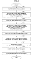
- a plasma processing method of the present embodiment including the above described processes (1) through (4) is described below with reference to FIG. 2 .
- the plasma processing method of the present embodiment can be performed by the plasma processing apparatus 10 of FIG. 1 or a different plasma processing apparatus.
- the wafer W is carried into the chamber 12 and placed on the mount table 20 (step S10).
- a gas (CF gas) including carbon (C) and fluorine (F) is introduced into the chamber 12, and high-frequency power RF (HF) is applied to the upper electrode 15 (step S12).
- CF gas including carbon (C) and fluorine (F)
- RF high-frequency power
- a CF film is formed on the upper electrode 15 by the generated plasma (step S14).
- an argon (Ar) gas is introduced into the chamber 12, and high-frequency power RF (HF) and direct-current (DC) power are applied to the upper electrode 15 (step S16).
- RF radio frequency
- DC direct-current
- step S18 the CF film on the upper electrode 15 is sputtered by the generated plasma.
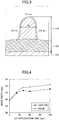
- FIG. 3 illustrates exemplary films formed on the wafer W.
- an organic film 130, an anti-reflection film 120, and a patterned ArF resist film 110 are formed on the wafer W.
- the ArF resist film 110 functions as a mask.
- a thin Si film with a thickness of several nm is formed on the ArF resist film 110.
- the plasma processing method of the present embodiment makes it possible to form a uniform thin film on a patterned mask formed on the wafer W to control a width W of the mask, and thereby makes it possible to form a finer pattern in the next etching process.
- step S22 etching is performed (step S22). After the etching, the wafer W is carried out of the chamber 12 (step S24). Then, wafer-less dry cleaning is performed (step S26), and the process ends.
- a plasma processing method is described above.
- the plasma processing method described above is just an example and may be modified.
- high-frequency power RF (HF) for plasma generation and direct-current power are applied to the upper electrode 15 at step S16 in FIG. 2
- a high-frequency power RF (HF) may be applied to the lower electrode 20, instead of applying a direct-current power to the upper electrode 15 at step S16.
- a film that functions as a target material is formed on the upper electrode 15, and the film is sputtered to form a uniform thin film on a pattern formed on the wafer W.
- This method makes it possible to control the width of a mask, and in the next step, perform fine processing on the wafer W using the width-controlled mask.
- the plasma processing method of the present embodiment also makes it possible to form a film for which no target material suitable to be place beforehand in a chamber, by forming a film to be used as a target material on the upper electrode 15.
- the plasma processing method makes it possible to perform sputter deposition regardless of the type of target material.
- the plasma processing method of the present embodiment makes it possible to form a uniform thin film regardless of the density of a pattern.
- the plasma processing method of the present embodiment makes it possible to perform fine processing on a wafer in a manner that satisfies current and future demands for miniaturization.
- film deposition on the upper electrode 15, sputtering, etching, and cleaning can be performed in the chamber 12 of the same plasma processing apparatus 10. Accordingly, the present embodiment makes it possible to reduce apparatus costs.
- a plasma processing apparatus and a plasma processing method according to an embodiment are described above.
- the present invention is not limited to the specifically disclosed embodiment, and variations and modifications may be made without departing from the scope of the present invention.
- the plasma processing method of the above embodiment may be performed not only by a capacitively-coupled plasma (CCP) apparatus, but also by other types of plasma processing apparatuses.
- CCP capacitively-coupled plasma
- other types of plasma processing apparatuses include an inductively-coupled plasma (ICP) apparatus, a chemical vapor deposition (CVD) apparatus using a radial line slot antenna, a helicon wave plasma (HWP) apparatus, and an electron cyclotron resonance (ECR) plasma apparatus.
- ICP inductively-coupled plasma
- CVD chemical vapor deposition
- HWP helicon wave plasma
- ECR electron cyclotron resonance
- a plasma processing apparatus includes a first high-frequency power supply that supplies first high-frequency power to an upper electrode, and at least one of a direct-current power supply that applies direct-current power to the upper electrode and a second high-frequency power supply that applies second high-frequency power with a frequency lower than that of the first high-frequency power to the lower electrode.
- the present invention may be applied not only to a plasma processing apparatus for processing a wafer, but also to a plasma processing apparatus for processing a large-size substrate for a flat panel display, an EL element, or a substrate for a solar battery.
Description
- An aspect of this disclosure relates to a plasma processing apparatus and a plasma processing method.
- There has been proposed a film-deposition method where a film is formed by applying direct-current power to a target material and sputtering the target material (see, for example, Japanese Laid-Open
Patent 15 Publications No.2009-280916 2004-2 66112 2009- 280916 - Further,
WO 2012/036936 A2 discloses methods of depositing metal in high aspect ratio features. In some embodiments, a method of processing a substrate includes applying RF power at VHF frequency to a target comprising metal disposed in the PVD chamber above the substrate to form a plasma from a plasma-forming gas, sputtering metal atoms from the target using the plasma while maintaining a first pressure in the PVD chamber sufficient to ionize a predominant portion of the sputtered metal atoms, depositing the ionized metal atoms on a bottom surface of the opening and on a first surface of the substrate, applying a first RF power to redistribute at least some of the deposited metal atoms from the bottom surface and upper surface to sidewalls of the opening, and repeating the deposition the redistribution processes until a first layer of metal is deposited on substantially all surfaces of the opening. -
US 2005/023130 A1 discloses a reactive sputtering apparatus, wherein an inert-gas supplying hole is provided in a movable target unit whose one end is open and whose conductance is controlled, and a reactive gas containing at least fluorine or oxygen can be supplied to a space between the target and a substrate. The apparatus is constructed so as to emit the reactive gas toward the substrate. A reactive-gas emitting location is in the space between the target and the substrate such that a concentration of the reactive gas on the substrate surface can be maintained at a higher level. When the target is moved, a reactive-gas emitting port is moved or the reactive-gas emitting location is changed. The concentration of the reactive gas on the substrate surface can be effectively kept constant, and a high-quality optical thin film can be formed. - A plasma processing apparatus according to the present invention is alternatively defined by the combination of features of claim 1 or claim 5. Dependent claims relate to preferred embodiments. A method according to the present invention is alternatively defined by the combination of features of claims 6 or of claim 7. The dependent claim relates to preferred embodiments.
- In an aspect of this disclosure, there is provided a plasma processing apparatus that includes a first electrode on which a substrate is placeable, a second electrode that is disposed to face the first electrode across a predetermined gap, a chamber that houses the first electrode and the second electrode, a first high-frequency power supply that supplies first high-frequency power to the second electrode, a direct- current power supply that supplies direct-current power to the second electrode, and a gas supply source. The plasma processing apparatus is configured to generate first plasma to form a film of a reaction product on the second electrode by causing the first high-frequency power supply to supply the first high-frequency power to the second electrode and causing the gas supply source to supply a first gas into the chamber; and generate second plasma to sputter the film of the reaction product on the second electrode by causing the first high-frequency power supply to supply the first high-frequency power to the second electrode, causing the direct-current power supply to supply the direct-current power to the second electrode, and causing the gas supply source to supply a second gas into the chamber.
-
-
FIG. 1 is a drawing illustrating an exemplary configuration of a plasma processing apparatus; -
FIG. 2 is a flowchart illustrating an exemplary plasma processing method; -
FIG. 3 is a drawing used to describe an effect of a plasma processing method of an embodiment; and -
FIG. 4 is a graph illustrating a relationship between a direct-current application time and a mask width. - In the related-art technologies of Japanese Laid-Open Patent Publications No.
2009-280916 2004-266112 - Accordingly, there is a demand for an apparatus and a method that can form, by sputter deposition, a film (e.g., a film including carbon (C) and fluorine (F)) for which no target material suitable to be placed beforehand in a chamber is available.
- An aspect of this disclosure provides a plasma processing apparatus and a plasma processing method that can form, by sputter deposition, a film for which no target material suitable to be placed beforehand in a chamber is available.
- Embodiments of the present invention are described below with reference to the accompanying drawings. Throughout the specification and the drawings, the same reference number is assigned to substantially the same components, and repeated descriptions of those components are omitted.
- An exemplary configuration of a
plasma processing apparatus 10 according to an embodiment is described below with reference toFIG. 1 . Theplasma processing apparatus 10 includes acylindrical chamber 12 comprised of a metal such as aluminum or stainless steel. Thechamber 12 is grounded. An opening is formed at the upper end of thechamber 12. Anupper electrode 15 is disposed at the opening via aninsulator 14. Theinsulator 14 and theupper electrode 15 constitute a lid for closing the opening of thechamber 12. - A mount table 12, on which a semiconductor wafer W (which is hereafter simply referred to as a "wafer W") is to be placed, is provided in the
chamber 12. The mount table 20 is comprised of, for example, aluminum and is supported via an insulating holder (not shown) by thechamber 12. Anelectrostatic chuck 22 for holding the wafer W is provided on an upper surface of the mount table 20. Theelectrostatic chuck 22 is configured to electrostatically attract and hold the wafer W on the mount table 20 with Coulomb force that is generated when direct-current power is applied to anelectrode plate 22a of theelectrostatic chuck 22. Afocus ring 26 is provided to surround the wafer W. Thefocus ring 26 may be comprised of silicon or quartz. - A high-
frequency power supply 28 is connected via a matching box (not shown) to the mount table 20. The high-frequency power supply 28 applies bias high-frequency power RF (LF) with a frequency of, for example, 400 kHz or greater to the mount table 20. With this configuration, the mount table 20 also functions as a lower electrode. - At the ceiling of the
chamber 12, theupper electrode 15 and an electrode support 16 for supporting theupper electrode 15 are provided. A surface of theupper electrode 15 faces the mount table 20, andmultiple gas holes 15a are formed in the surface of theupper electrode 15. Theupper electrode 15 may be comprised of a material such as silicon (Si), silicon carbide (SiC), or quartz (SiO2). Theelectrode support 16 supports theupper electrode 15, and may be comprised of a conductive material such as aluminum. - A gas output from a
gas supply source 32 flows through agas diffusion chamber 30 and is supplied in the form of a shower into thechamber 12 from thegas holes 15a. Thus, theupper electrode 15 also functions as a shower head. - High-frequency power RF (HF) for plasma generation with a frequency of, for example, 60 MHz is applied from a high-
frequency power supply 18 via a matching box (not shown) to theupper electrode 15. With this configuration, the high-frequency power from the high-frequency power supply 18 is applied to a "capacitor" formed between the mount table 20 and the shower head. The high-frequency power supply 18 supplies high-frequency power with a frequency higher than the frequency of the high-frequency power supplied by the high-frequency power supply 28. - The lower electrode (mount table 20) is an example of a first electrode on which the wafer W is placed. The
upper electrode 15 is an example of a second electrode that is disposed to face the lower electrode. The high-frequency power supply 18 is an example of a first high-frequency power supply that supplies first high-frequency power to theupper electrode 15. The high-frequency power supply 28 is an example of a second high-frequency power supply that supplies second high-frequency power with a frequency lower than the first high-frequency power. - Sputtering described later is performed by applying direct-current (DC) power supplied from a direct-
current power supply 19 to theupper electrode 15. In this case, theupper electrode 15 is preferably comprised of a silicon (Si) material. Sputtering may also be performed by applying bias high-frequency power with a frequency of, for example, about 400 kHz to thelower electrode 20. In this case, thelower electrode 20 is not necessarily comprised of silicon, but may instead be comprised of quartz. The direct-current power supply 19 is an example of a direct-current power supply that supplies direct-current power to theupper electrode 15. - An
evacuation channel 34 is formed between a side wall of the mount table 20 and an inner wall of thechamber 12. Abaffle board 36 is provided in theevacuation channel 34 to regulate the flow of gas. A gas in thechamber 12 is exhausted from thechamber 12 by an evacuation device (not shown) through theevacuation channel 34 to reduce the pressure in thechamber 12 to a predetermined vacuum pressure. - The
plasma processing apparatus 10 also includes acontroller 200 for controlling operations of the entireplasma processing apparatus 10. Thecontroller 200 includes a central processing unit (CPU) 205, a read-only memory (ROM) 210, a random access memory (RAM) 215, and a hard disk drive (HDD) 220. TheCPU 205 performs plasma processing described later according to various recipes. A recipe includes control information for controlling theplasma processing apparatus 10 to perform a process. For example, the control information includes process time, a pressure (gas exhaust), high-frequency power and voltage, flow rates of various process gases, and temperatures in a chamber (e.g., an upper electrode temperature, a temperature of a side wall of the chamber, and an ESC temperature). The recipes may be stored in theRAM 215, theHDD 220, or a semiconductor memory (not shown). Also, the recipes may be stored in a portable, computer-readable storage medium such as a compact disk read-only memory (CD-ROM) or a digital versatile disk (DVD). - An exemplary configuration of the
plasma processing apparatus 10 of the present embodiment is described above. In theplasma processing apparatus 10 configured as described above, the wafer W is carried into thechamber 12 via agate valve 40 and placed on theelectrostatic chuck 22. In this state, gases and high-frequency power are supplied to generate plasma; and using the generated plasma, (1) an upper electrode film deposition process, (2) a wafer film deposition process, (3) an etching process, and (4) a wafer-less dry cleaning process are performed in sequence in thesame chamber 12. - In the upper electrode film deposition process of the present embodiment, the
plasma processing apparatus 10 generates plasma by supplying a film deposition gas (first gas) and high-frequency power RF (HF) to theupper electrode 15. By the action of the generated plasma, a film of a reaction product is formed mainly on a lower surface of theupper electrode 15. - In the present embodiment, a gap between the
upper electrode 15 and the mount table 20 is set at 80 mm or greater. With the wide gap set at 80 mm or greater, when the pressure in thechamber 12 is high (e.g., 13.3 Pa or higher), the gas density increases, the mean free path of gas molecules becomes short, and the frequency of molecular collisions becomes high. Because the frequency of collisions between radicals and ions in the plasma also becomes high, the plasma is deactivated and becomes unable to diffuse. Accordingly, the plasma is generated mainly near theupper electrode 15. For the above reasons, the reaction product generated from the plasma is deposited mostly on a plasma surface of theupper electrode 15 facing the mount table 20, and does not reach the upper surface of the wafer W. Thus, through the above process, a film of the reaction product is formed on theupper electrode 15. - The film of the reaction product formed on the
upper electrode 15 may be, for example, a silicon (Si) film, a carbon (C) film, a CF film including carbon (C) and fluorine (F), a silicon-containing film such as an SiO2 film, or a carbon-containing film. - For example, when a CF film is to be formed on the
upper electrode 15, a single gas such as a C4F8 gas, a CHF3 gas, or a CH2F2 gas, or a mixed gas including at least one of these gases may be supplied as the film deposition gas into thechamber 12. - Here, for a CF film in particular, there is no target material suitable to be placed beforehand in the
chamber 12. With theplasma processing apparatus 10 of the present embodiment, it is possible to form a CF film on the wafer W by forming the CF film in thechamber 12 and then sputtering the CF film in thesame chamber 12. Thus, theplasma processing apparatus 10 of the present embodiment can form a film by sputtering, regardless of the type of target material. - Also, when the
upper electrode 15 is comprised of quartz (SiO2), it is possible to form an SiO film on the wafer W by forming an Si film or an Si-containing film as a reaction product film on theupper electrode 15. - In the wafer film deposition process of the present embodiment, the
plasma processing apparatus 10 generates plasma by supplying a sputtering gas (second gas), high-frequency power RF (HF), and direct-current power to theupper electrode 15. By the action of the generated plasma (particularly, by the bombardment of ions in the plasma), the film of the reaction product formed on theupper electrode 15 is sputtered. Thus, after the film of the reaction product is formed on theupper electrode 15 in thechamber 12, the film of the reaction product on theupper electrode 15 is sputtered in thesame chamber 12. The sputtered reaction product is deposited on the wafer W placed on the mount table 20, and a uniform thin film is formed on the wafer W. - In addition to or instead of supplying the direct-current power to the
upper electrode 15, high-frequency power RF (HF) may be supplied from the high-frequency power supply 28 to the mount table 20 (lower electrode) when sputtering the film of the reaction product. - Examples of the sputtering gas to be supplied into the
chamber 12 include a single inert gas such as an argon (Ar) gas and a mixed inert gas such as a mixture of an argon gas and a hydrogen (H2) gas. - The thickness of a sheath formed on the lower surface of the
upper electrode 15 and the inner wall of thechamber 12 can be controlled by controlling the value of the direct-current power applied to theupper electrode 15. For example, compared with a case where the direct-current power is not applied, the thickness of the sheath becomes greater when the direct-current power is applied to theupper electrode 15. Also, the thickness of the sheath increases as the value of the applied direct-current power increases. As the thickness of the sheath increases, the sheath voltage increases, and ions in the plasma are accelerated in the sheath. This in turn makes it possible to cause the ions to strongly collide with the surface of theupper electrode 15, and thereby improve sputtering efficiency. Generally, the thickness of a sheath is determined by an acceleration voltage (a DC voltage or high-frequency power RF (LF) with a frequency lower than 1 MHz), a plasma density, and an electron temperature of plasma. Accordingly, it is possible to control a sputtering process by varying a sheath voltage by controlling the value of direct-current power. - As described above, in the
plasma processing apparatus 10 of the present embodiment, a film of a target material such as a CF film, which is not suitable to be placed beforehand in thechamber 12, is formed on theupper electrode 15. Next, the film formed on theupper electrode 15 is sputtered to remove (or blow off) atoms and molecules in the film from theupper electrode 15. The removed atoms and molecules jump between theupper electrode 15 and the mount table 20, reach and adhere to the wafer W, and form a film on the wafer W. - For example, when a pattern of a resist film is formed on the wafer W, the atoms and molecules removed by the sputtering from the film on the
upper electrode 15 fly to the wafer W and form a film on the resist film. This makes it possible to increase the width of the resist film by an amount corresponding to the thickness of the formed film. For example, when a CF film is formed as a reaction product film, a uniform thin CF film is formed on the resist film. As a result, in the next etching process performed using the resist film as a mask, the diameter of a hole or the width of a line to be etched is decreased by an amount corresponding to the increase in the width of the resist film. Thus, this approach enables fine processing - As described above, in the present embodiment, a film of a reaction product to be used as a target material is formed on the
upper electrode 15, and then the film is sputtered so that a uniform thin film is formed on the wafer W with diffused atoms and molecules of the sputtered film. As another method, a desired film may be directly formed on the wafer W by chemical vapor deposition (CVD). - As a technique for fine processing, there exists a pattern shrink technology that makes it possible to form patterns finer than those formed by lithography. In the pattern shrink technology, a pattern is etched by plasma etching using a deposition etching gas such that a desired deposit is formed on the etched pattern. This makes it possible to reduce, for example, the diameter of a hole and the width of a line formed by etching. However, the adherence of the deposit formed by plasma etching shows anisotropy, and the amount of deposit varies depending on the density of a pattern. More specifically, in an area where the pattern is thin, the amount of deposit becomes greater and the film thickness becomes greater; and in an area where the pattern is dense, the amount of deposit becomes smaller and the film thickness becomes smaller. This results in formation of an uneven film, and affects the next etching process. Thus, with the related-art pattern shrink technology, it will be difficult to meet the future demand for finer wafer processing.
- There is a growing demand for further miniaturization, and the International Technology Roadmap for Semiconductors (ITRS) expects that miniaturization advances year by year. However, with the technology where a film is formed while performing etching using a deposition etching gas, it is difficult to form a uniform film that satisfies such a demand for miniaturization.
- Also, it is thought that formation of lines with a half pitch (hp) of about 40 nm is the limit of the current ArF immersion exposure technology. Therefore, to form a finer pattern, a technique such as double patterning has been introduced. Thus, to meet the market needs, shrink technologies for forming patterns finer than those formed by lithography have become important.
- The
plasma processing apparatus 10 of the present embodiment enables a shrink technology where a deposition process and a sputtering process for a target material are performed in thesame chamber 12. This technology makes it possible to form a uniform film on a resist film, and to accurately perform an etching process that satisfies miniaturization demands. For example, the present embodiment makes it possible to form a uniform film with a thickness of about several nm to several tens nm on a fine resist film formed by double patterning. Thus, the present embodiment provides a technology that is particularly suitable to increase the fineness of a pattern formed by double patterning. - After the etched wafer W is carried out of the
chamber 12, it is preferable to perform a wafer-less dry cleaning (WLDC) process. For example, a CF film in thechamber 12 can be removed by using O2 plasma. The processes (1) through (4) described above are performed in the sameplasma processing apparatus 10. - A plasma processing method of the present embodiment including the above described processes (1) through (4) is described below with reference to
FIG. 2 . The plasma processing method of the present embodiment can be performed by theplasma processing apparatus 10 ofFIG. 1 or a different plasma processing apparatus. - When the plasma processing method is started, the wafer W is carried into the
chamber 12 and placed on the mount table 20 (step S10). - Next, a gas (CF gas) including carbon (C) and fluorine (F) is introduced into the
chamber 12, and high-frequency power RF (HF) is applied to the upper electrode 15 (step S12). As a result, from the CF gas, plasma including radicals and ions of C and F is generated. - Next, a CF film is formed on the
upper electrode 15 by the generated plasma (step S14). - Next, an argon (Ar) gas is introduced into the
chamber 12, and high-frequency power RF (HF) and direct-current (DC) power are applied to the upper electrode 15 (step S16). As a result, plasma is generated from the argon gas. - Next, the CF film on the
upper electrode 15 is sputtered by the generated plasma (step S18). - Atoms and molecules removed from the CF film as a result of the sputtering fly and adhere to the wafer W. As a result, a thin CF film is formed on a resist film (mask) formed on the wafer W.
FIG. 3 illustrates exemplary films formed on the wafer W. In this example, anorganic film 130, ananti-reflection film 120, and a patterned ArF resistfilm 110 are formed on the wafer W. The ArF resistfilm 110 functions as a mask. In the example ofFIG. 3 , a thin Si film with a thickness of several nm is formed on the ArF resistfilm 110. Thus, the plasma processing method of the present embodiment makes it possible to form a uniform thin film with a thickness of about several nm.FIG. 4 is a graph illustrating a relationship between a direct-current application time and a mask width. This graph indicates that it is possible to form a thin film with a thickness of about 2.5 nm on a mask and thereby increase the width of the mask by about 5 nm by applying direct-current voltage for about 30 seconds. Thus, the plasma processing method of the present embodiment makes it possible to form a uniform thin film on a patterned mask formed on the wafer W to control a width W of the mask, and thereby makes it possible to form a finer pattern in the next etching process. - Referring back to
FIG. 2 , after step S20, etching is performed (step S22). After the etching, the wafer W is carried out of the chamber 12 (step S24). Then, wafer-less dry cleaning is performed (step S26), and the process ends. - A plasma processing method according to the present embodiment is described above. However, the plasma processing method described above is just an example and may be modified. For example, although high-frequency power RF (HF) for plasma generation and direct-current power are applied to the
upper electrode 15 at step S16 inFIG. 2 , a high-frequency power RF (HF) may be applied to thelower electrode 20, instead of applying a direct-current power to theupper electrode 15 at step S16. - As described above, in the plasma processing method of the present embodiment, a film that functions as a target material is formed on the
upper electrode 15, and the film is sputtered to form a uniform thin film on a pattern formed on the wafer W. This method makes it possible to control the width of a mask, and in the next step, perform fine processing on the wafer W using the width-controlled mask. - The plasma processing method of the present embodiment also makes it possible to form a film for which no target material suitable to be place beforehand in a chamber, by forming a film to be used as a target material on the
upper electrode 15. Thus, the plasma processing method makes it possible to perform sputter deposition regardless of the type of target material. - With the related-art CVD method, the thickness of a film to be formed on a pattern varies depending on the density of the pattern. Therefore, with the related-art CVD method, it is difficult to meet the feature demand for finer wafer processing. On the other hand, the plasma processing method of the present embodiment makes it possible to form a uniform thin film regardless of the density of a pattern. Thus, the plasma processing method of the present embodiment makes it possible to perform fine processing on a wafer in a manner that satisfies current and future demands for miniaturization.
- Also according to the present embodiment, film deposition on the
upper electrode 15, sputtering, etching, and cleaning can be performed in thechamber 12 of the sameplasma processing apparatus 10. Accordingly, the present embodiment makes it possible to reduce apparatus costs. - A plasma processing apparatus and a plasma processing method according to an embodiment are described above. However, the present invention is not limited to the specifically disclosed embodiment, and variations and modifications may be made without departing from the scope of the present invention.
- For example, the plasma processing method of the above embodiment may be performed not only by a capacitively-coupled plasma (CCP) apparatus, but also by other types of plasma processing apparatuses. Examples of other types of plasma processing apparatuses include an inductively-coupled plasma (ICP) apparatus, a chemical vapor deposition (CVD) apparatus using a radial line slot antenna, a helicon wave plasma (HWP) apparatus, and an electron cyclotron resonance (ECR) plasma apparatus.
- A plasma processing apparatus according to an aspect of this disclosure includes a first high-frequency power supply that supplies first high-frequency power to an upper electrode, and at least one of a direct-current power supply that applies direct-current power to the upper electrode and a second high-frequency power supply that applies second high-frequency power with a frequency lower than that of the first high-frequency power to the lower electrode.
- The present invention may be applied not only to a plasma processing apparatus for processing a wafer, but also to a plasma processing apparatus for processing a large-size substrate for a flat panel display, an EL element, or a substrate for a solar battery.
Claims (8)
- A plasma processing apparatus (10), comprising:a first electrode (20) on which a substrate (W) is placeable;a second electrode (15) that is disposed to face the first electrode (20) across a predetermined gap;a chamber (12) that houses the first electrode (20) and the second electrode (15);a first high-frequency power supply (18) that supplies first high-frequency power to the second electrode (15);a direct-current power supply (19) that supplies direct-current power to the second electrode (15); anda gas supply source (32),characterized in that the plasma processing apparatus (10) is configured togenerate first plasma to form a film of a reaction product on the second electrode (15) by causing the first high-frequency power supply (18) to supply the first high-frequency power to the second electrode (15) and causing the gas supply source (32) to supply a first gas into the chamber (12), andgenerate second plasma to sputter the film of the reaction product on the second electrode (15) by causing the first high-frequency power supply (18) to supply the first high-frequency power to the second electrode (15), causing the direct-current power supply (19) to supply the direct-current power to the second electrode (15), and causing the gas supply source (32) to supply a second gas into the chamber (12).
- The plasma processing apparatus as claimed in claim 1, further comprising:a second high-frequency power supply (28) that supplies second high-frequency power to the first electrode (20), the second high-frequency power having a frequency lower than a frequency of the first high- frequency power,wherein the plasma processing apparatus (10) is configured to cause the second high-frequency power supply (28) to supply the second high-frequency power to the first electrode (20) when sputtering the film of the reaction product.
- The plasma processing apparatus as claimed in claim 1 or 2, wherein the gap between the first electrode (20) and the second electrode (15) is greater than or equal to 80 mm.
- The plasma processing apparatus as claimed in any one of claims 1 through 3, wherein the plasma processing apparatus (10) is configured to sputter the film of the reaction product on the second electrode (15) in the chamber (12) to form a film on the substrate (W) placed on the first electrode (20), after forming the film of the reaction product on the second electrode (15) in the same chamber (12).
- A plasma processing apparatus (10), comprising:a first electrode (20) on which a substrate (W) is placeable;a second electrode (15) that is disposed to face the first electrode (20) across a predetermined gap;a chamber (12) that houses the first electrode (20) and the second electrode (15);a first high-frequency power supply (18) that supplies first high-frequency power to the second electrode (15);a second high-frequency power supply (28) that supplies second high-frequency power to the first electrode (20), the second high-frequency power having a frequency lower than a frequency of the first high-frequency power; anda gas supply source (32),characterized in that the plasma processing apparatus (10) is configured togenerate first plasma to form a film of a reaction product on the second electrode (15) by causing the first high-frequency power supply (18) to supply the first high-frequency power to the second electrode (15) and causing the gas supply source (32) to supply a first gas into the chamber (12), andgenerate second plasma to sputter the film of the reaction product on the second electrode (15) by causing the first high-frequency power supply (18) to supply the first high-frequency power (18) to the second electrode (15), causing the second high-frequency power supply (28) to supply the second high-frequency power to the first electrode (20), and causing the gas supply source (32) to supply a second gas into the chamber (12).
- A method performed by a plasma processing apparatus (10) including a first electrode (20) on which a substrate (W) is placed, a second electrode (15) disposed to face the first electrode (20) across a predetermined gap, and a chamber (12) housing the first electrode (20) and the second electrode (15), the method being characterized by comprising:generating first plasma to form a film of a reaction product on the second electrode (15) by supplying first high-frequency power to the second electrode (15) and supplying a first gas into the chamber (12) andgenerating second plasma to sputter the film of the reaction product on the second electrode (15) by supplying the first high-frequency power and a direct-current power to the second electrode (15) and supplying a second gas into the chamber (12).
- A method performed by a plasma processing apparatus (10) including a first electrode (20) on which a substrate (W) is placed, a second electrode (15) disposed to face the first electrode (20) across a predetermined gap, and a chamber (12) housing the first electrode (20) and the second electrode (15), the method being characterized by comprising:generating first plasma to form a film of a reaction product on the second electrode (15) by supplying first high-frequency power to the second electrode (15) and supplying a first gas into the chamber (12); andgenerating second plasma to sputter the film of the reaction product on the second electrode (15) by supplying the first high-frequency power to the second electrode (15), supplying second high-frequency power to the first electrode (20), and supplying a second gas into the chamber (12),wherein the second high-frequency power has a frequency lower than a frequency of the first high- frequency power.
- The method performed by a plasma processing apparatus as claimed in claim 6 or 7, wherein the film of the reaction product includes carbon and fluorine.
Applications Claiming Priority (1)
| Application Number | Priority Date | Filing Date | Title |
|---|---|---|---|
| JP2014153894A JP6329839B2 (en) | 2014-07-29 | 2014-07-29 | Plasma processing apparatus and plasma processing method |
Publications (2)
| Publication Number | Publication Date |
|---|---|
| EP2980829A1 EP2980829A1 (en) | 2016-02-03 |
| EP2980829B1 true EP2980829B1 (en) | 2018-05-09 |
Family
ID=53724127
Family Applications (1)
| Application Number | Title | Priority Date | Filing Date |
|---|---|---|---|
| EP15178628.2A Not-in-force EP2980829B1 (en) | 2014-07-29 | 2015-07-28 | Plasma processing apparatus and plasma processing method |
Country Status (7)
| Country | Link |
|---|---|
| US (1) | US10233535B2 (en) |
| EP (1) | EP2980829B1 (en) |
| JP (1) | JP6329839B2 (en) |
| KR (1) | KR102364534B1 (en) |
| CN (1) | CN105316639B (en) |
| SG (1) | SG10201505886XA (en) |
| TW (1) | TWI682426B (en) |
Families Citing this family (4)
| Publication number | Priority date | Publication date | Assignee | Title |
|---|---|---|---|---|
| US10563304B2 (en) * | 2017-04-07 | 2020-02-18 | Applied Materials, Inc. | Methods and apparatus for dynamically treating atomic layer deposition films in physical vapor deposition chambers |
| JP6883495B2 (en) * | 2017-09-04 | 2021-06-09 | 東京エレクトロン株式会社 | Etching method |
| DE102017124682B4 (en) * | 2017-10-23 | 2019-06-27 | RF360 Europe GmbH | A wafer carrier, method of removing material from an upper surface of a wafer, and method of adding material to a wafer |
| CN115247257B (en) * | 2021-04-25 | 2024-01-23 | 广东聚华印刷显示技术有限公司 | Film forming apparatus and method for producing film |
Family Cites Families (16)
| Publication number | Priority date | Publication date | Assignee | Title |
|---|---|---|---|---|
| US5962923A (en) * | 1995-08-07 | 1999-10-05 | Applied Materials, Inc. | Semiconductor device having a low thermal budget metal filling and planarization of contacts, vias and trenches |
| US20030116427A1 (en) * | 2001-08-30 | 2003-06-26 | Applied Materials, Inc. | Self-ionized and inductively-coupled plasma for sputtering and resputtering |
| JP2002110650A (en) * | 2000-10-03 | 2002-04-12 | Tokyo Electron Ltd | Plasma etching method and plasma etching apparatus |
| US6709553B2 (en) | 2002-05-09 | 2004-03-23 | Applied Materials, Inc. | Multiple-step sputter deposition |
| AU2003244166A1 (en) * | 2002-06-27 | 2004-01-19 | Tokyo Electron Limited | Plasma processing method |
| JP4497447B2 (en) | 2003-03-03 | 2010-07-07 | 株式会社アルバック | Pulsed DC sputtering film forming method and film forming apparatus for the method |
| JP2005048260A (en) | 2003-07-31 | 2005-02-24 | Canon Inc | Reactive sputtering method |
| US7235160B2 (en) * | 2003-08-06 | 2007-06-26 | Energy Photovoltaics, Inc. | Hollow cathode sputtering apparatus and related method |
| JP4646053B2 (en) * | 2004-09-29 | 2011-03-09 | 株式会社アルバック | Branch switch and etching apparatus for high frequency power |
| JP5323306B2 (en) * | 2006-07-12 | 2013-10-23 | 東京エレクトロン株式会社 | Plasma etching method and computer-readable storage medium |
| JP2008028022A (en) * | 2006-07-19 | 2008-02-07 | Tokyo Electron Ltd | Plasma etching method and computer readable storage medium |
| JP4613243B2 (en) | 2009-07-14 | 2011-01-12 | 株式会社アルバック | Pulsed DC sputtering film forming method and film forming apparatus for the method |
| US8846451B2 (en) | 2010-07-30 | 2014-09-30 | Applied Materials, Inc. | Methods for depositing metal in high aspect ratio features |
| US8563428B2 (en) | 2010-09-17 | 2013-10-22 | Applied Materials, Inc. | Methods for depositing metal in high aspect ratio features |
| JP5405504B2 (en) * | 2011-01-31 | 2014-02-05 | 東京エレクトロン株式会社 | Plasma processing apparatus and plasma processing method |
| JP6063264B2 (en) * | 2012-09-13 | 2017-01-18 | 東京エレクトロン株式会社 | Method for processing substrate and plasma processing apparatus |
-
2014
- 2014-07-29 JP JP2014153894A patent/JP6329839B2/en active Active
-
2015
- 2015-07-15 US US14/799,650 patent/US10233535B2/en active Active
- 2015-07-27 TW TW104124201A patent/TWI682426B/en active
- 2015-07-28 KR KR1020150106221A patent/KR102364534B1/en active IP Right Grant
- 2015-07-28 EP EP15178628.2A patent/EP2980829B1/en not_active Not-in-force
- 2015-07-28 SG SG10201505886XA patent/SG10201505886XA/en unknown
- 2015-07-29 CN CN201510455789.4A patent/CN105316639B/en active Active
Non-Patent Citations (1)
| Title |
|---|
| None * |
Also Published As
| Publication number | Publication date |
|---|---|
| EP2980829A1 (en) | 2016-02-03 |
| JP2016032028A (en) | 2016-03-07 |
| CN105316639A (en) | 2016-02-10 |
| US10233535B2 (en) | 2019-03-19 |
| KR20160014543A (en) | 2016-02-11 |
| KR102364534B1 (en) | 2022-02-17 |
| JP6329839B2 (en) | 2018-05-23 |
| US20160032445A1 (en) | 2016-02-04 |
| CN105316639B (en) | 2018-06-08 |
| SG10201505886XA (en) | 2016-02-26 |
| TW201618156A (en) | 2016-05-16 |
| TWI682426B (en) | 2020-01-11 |
Similar Documents
| Publication | Publication Date | Title |
|---|---|---|
| JP6385915B2 (en) | Etching method | |
| US9659756B2 (en) | Plasma etching apparatus and plasma cleaning method | |
| TWI723049B (en) | Methods for atomic level resolution and plasma processing control | |
| JP6568822B2 (en) | Etching method | |
| US20200381263A1 (en) | Method of processing target object | |
| EP3051576B1 (en) | Method of processing a target object comprising forming a silicon oxide film | |
| JP6438831B2 (en) | Method for etching an organic film | |
| JP6366454B2 (en) | Method for processing an object | |
| JP2008078515A (en) | Plasma treatment method | |
| US11462412B2 (en) | Etching method | |
| EP2980829B1 (en) | Plasma processing apparatus and plasma processing method | |
| WO2014034396A1 (en) | Plasma processing method and plasma processing device | |
| JP2018195846A (en) | Etching apparatus | |
| US20210327719A1 (en) | Method for processing workpiece | |
| JP2016086046A (en) | Plasma processing method | |
| JP2020088174A (en) | Etching method and substrate processing apparatus | |
| JP2023053351A (en) | Plasma processing apparatus |
Legal Events
| Date | Code | Title | Description |
|---|---|---|---|
| PUAI | Public reference made under article 153(3) epc to a published international application that has entered the european phase |
Free format text: ORIGINAL CODE: 0009012 |
|
| 17P | Request for examination filed |
Effective date: 20150728 |
|
| AK | Designated contracting states |
Kind code of ref document: A1 Designated state(s): AL AT BE BG CH CY CZ DE DK EE ES FI FR GB GR HR HU IE IS IT LI LT LU LV MC MK MT NL NO PL PT RO RS SE SI SK SM TR |
|
| AX | Request for extension of the european patent |
Extension state: BA ME |
|
| REG | Reference to a national code |
Ref country code: DE Ref legal event code: R079 Ref document number: 602015010872 Country of ref document: DE Free format text: PREVIOUS MAIN CLASS: H01J0037340000 Ipc: C23C0014060000 |
|
| RIC1 | Information provided on ipc code assigned before grant |
Ipc: H01L 31/18 20060101ALI20170630BHEP Ipc: H01J 37/32 20060101ALI20170630BHEP Ipc: C23C 14/06 20060101AFI20170630BHEP Ipc: H01J 37/34 20060101ALI20170630BHEP Ipc: C23C 14/34 20060101ALI20170630BHEP Ipc: C23C 16/509 20060101ALI20170630BHEP Ipc: C23C 16/30 20060101ALI20170630BHEP |
|
| GRAP | Despatch of communication of intention to grant a patent |
Free format text: ORIGINAL CODE: EPIDOSNIGR1 |
|
| INTG | Intention to grant announced |
Effective date: 20180104 |
|
| GRAJ | Information related to disapproval of communication of intention to grant by the applicant or resumption of examination proceedings by the epo deleted |
Free format text: ORIGINAL CODE: EPIDOSDIGR1 |
|
| GRAR | Information related to intention to grant a patent recorded |
Free format text: ORIGINAL CODE: EPIDOSNIGR71 |
|
| GRAS | Grant fee paid |
Free format text: ORIGINAL CODE: EPIDOSNIGR3 |
|
| GRAA | (expected) grant |
Free format text: ORIGINAL CODE: 0009210 |
|
| INTC | Intention to grant announced (deleted) | ||
| AK | Designated contracting states |
Kind code of ref document: B1 Designated state(s): AL AT BE BG CH CY CZ DE DK EE ES FI FR GB GR HR HU IE IS IT LI LT LU LV MC MK MT NL NO PL PT RO RS SE SI SK SM TR |
|
| INTG | Intention to grant announced |
Effective date: 20180404 |
|
| REG | Reference to a national code |
Ref country code: GB Ref legal event code: FG4D |
|
| REG | Reference to a national code |
Ref country code: CH Ref legal event code: EP Ref country code: AT Ref legal event code: REF Ref document number: 997633 Country of ref document: AT Kind code of ref document: T Effective date: 20180515 |
|
| REG | Reference to a national code |
Ref country code: IE Ref legal event code: FG4D |
|
| REG | Reference to a national code |
Ref country code: DE Ref legal event code: R096 Ref document number: 602015010872 Country of ref document: DE |
|
| REG | Reference to a national code |
Ref country code: NL Ref legal event code: MP Effective date: 20180509 |
|
| REG | Reference to a national code |
Ref country code: LT Ref legal event code: MG4D |
|
| PG25 | Lapsed in a contracting state [announced via postgrant information from national office to epo] |
Ref country code: LT Free format text: LAPSE BECAUSE OF FAILURE TO SUBMIT A TRANSLATION OF THE DESCRIPTION OR TO PAY THE FEE WITHIN THE PRESCRIBED TIME-LIMIT Effective date: 20180509 Ref country code: ES Free format text: LAPSE BECAUSE OF FAILURE TO SUBMIT A TRANSLATION OF THE DESCRIPTION OR TO PAY THE FEE WITHIN THE PRESCRIBED TIME-LIMIT Effective date: 20180509 Ref country code: BG Free format text: LAPSE BECAUSE OF FAILURE TO SUBMIT A TRANSLATION OF THE DESCRIPTION OR TO PAY THE FEE WITHIN THE PRESCRIBED TIME-LIMIT Effective date: 20180809 Ref country code: FI Free format text: LAPSE BECAUSE OF FAILURE TO SUBMIT A TRANSLATION OF THE DESCRIPTION OR TO PAY THE FEE WITHIN THE PRESCRIBED TIME-LIMIT Effective date: 20180509 Ref country code: NO Free format text: LAPSE BECAUSE OF FAILURE TO SUBMIT A TRANSLATION OF THE DESCRIPTION OR TO PAY THE FEE WITHIN THE PRESCRIBED TIME-LIMIT Effective date: 20180809 Ref country code: SE Free format text: LAPSE BECAUSE OF FAILURE TO SUBMIT A TRANSLATION OF THE DESCRIPTION OR TO PAY THE FEE WITHIN THE PRESCRIBED TIME-LIMIT Effective date: 20180509 |
|
| PG25 | Lapsed in a contracting state [announced via postgrant information from national office to epo] |
Ref country code: GR Free format text: LAPSE BECAUSE OF FAILURE TO SUBMIT A TRANSLATION OF THE DESCRIPTION OR TO PAY THE FEE WITHIN THE PRESCRIBED TIME-LIMIT Effective date: 20180810 Ref country code: LV Free format text: LAPSE BECAUSE OF FAILURE TO SUBMIT A TRANSLATION OF THE DESCRIPTION OR TO PAY THE FEE WITHIN THE PRESCRIBED TIME-LIMIT Effective date: 20180509 Ref country code: RS Free format text: LAPSE BECAUSE OF FAILURE TO SUBMIT A TRANSLATION OF THE DESCRIPTION OR TO PAY THE FEE WITHIN THE PRESCRIBED TIME-LIMIT Effective date: 20180509 Ref country code: HR Free format text: LAPSE BECAUSE OF FAILURE TO SUBMIT A TRANSLATION OF THE DESCRIPTION OR TO PAY THE FEE WITHIN THE PRESCRIBED TIME-LIMIT Effective date: 20180509 Ref country code: NL Free format text: LAPSE BECAUSE OF FAILURE TO SUBMIT A TRANSLATION OF THE DESCRIPTION OR TO PAY THE FEE WITHIN THE PRESCRIBED TIME-LIMIT Effective date: 20180509 |
|
| REG | Reference to a national code |
Ref country code: AT Ref legal event code: MK05 Ref document number: 997633 Country of ref document: AT Kind code of ref document: T Effective date: 20180509 |
|
| PG25 | Lapsed in a contracting state [announced via postgrant information from national office to epo] |
Ref country code: DK Free format text: LAPSE BECAUSE OF FAILURE TO SUBMIT A TRANSLATION OF THE DESCRIPTION OR TO PAY THE FEE WITHIN THE PRESCRIBED TIME-LIMIT Effective date: 20180509 Ref country code: PL Free format text: LAPSE BECAUSE OF FAILURE TO SUBMIT A TRANSLATION OF THE DESCRIPTION OR TO PAY THE FEE WITHIN THE PRESCRIBED TIME-LIMIT Effective date: 20180509 Ref country code: SK Free format text: LAPSE BECAUSE OF FAILURE TO SUBMIT A TRANSLATION OF THE DESCRIPTION OR TO PAY THE FEE WITHIN THE PRESCRIBED TIME-LIMIT Effective date: 20180509 Ref country code: RO Free format text: LAPSE BECAUSE OF FAILURE TO SUBMIT A TRANSLATION OF THE DESCRIPTION OR TO PAY THE FEE WITHIN THE PRESCRIBED TIME-LIMIT Effective date: 20180509 Ref country code: CZ Free format text: LAPSE BECAUSE OF FAILURE TO SUBMIT A TRANSLATION OF THE DESCRIPTION OR TO PAY THE FEE WITHIN THE PRESCRIBED TIME-LIMIT Effective date: 20180509 Ref country code: EE Free format text: LAPSE BECAUSE OF FAILURE TO SUBMIT A TRANSLATION OF THE DESCRIPTION OR TO PAY THE FEE WITHIN THE PRESCRIBED TIME-LIMIT Effective date: 20180509 Ref country code: AT Free format text: LAPSE BECAUSE OF FAILURE TO SUBMIT A TRANSLATION OF THE DESCRIPTION OR TO PAY THE FEE WITHIN THE PRESCRIBED TIME-LIMIT Effective date: 20180509 |
|
| REG | Reference to a national code |
Ref country code: DE Ref legal event code: R097 Ref document number: 602015010872 Country of ref document: DE |
|
| PG25 | Lapsed in a contracting state [announced via postgrant information from national office to epo] |
Ref country code: SM Free format text: LAPSE BECAUSE OF FAILURE TO SUBMIT A TRANSLATION OF THE DESCRIPTION OR TO PAY THE FEE WITHIN THE PRESCRIBED TIME-LIMIT Effective date: 20180509 Ref country code: IT Free format text: LAPSE BECAUSE OF FAILURE TO SUBMIT A TRANSLATION OF THE DESCRIPTION OR TO PAY THE FEE WITHIN THE PRESCRIBED TIME-LIMIT Effective date: 20180509 |
|
| REG | Reference to a national code |
Ref country code: CH Ref legal event code: PL |
|
| PLBE | No opposition filed within time limit |
Free format text: ORIGINAL CODE: 0009261 |
|
| STAA | Information on the status of an ep patent application or granted ep patent |
Free format text: STATUS: NO OPPOSITION FILED WITHIN TIME LIMIT |
|
| PG25 | Lapsed in a contracting state [announced via postgrant information from national office to epo] |
Ref country code: LU Free format text: LAPSE BECAUSE OF NON-PAYMENT OF DUE FEES Effective date: 20180728 Ref country code: MC Free format text: LAPSE BECAUSE OF FAILURE TO SUBMIT A TRANSLATION OF THE DESCRIPTION OR TO PAY THE FEE WITHIN THE PRESCRIBED TIME-LIMIT Effective date: 20180509 |
|
| REG | Reference to a national code |
Ref country code: BE Ref legal event code: MM Effective date: 20180731 |
|
| 26N | No opposition filed |
Effective date: 20190212 |
|
| PG25 | Lapsed in a contracting state [announced via postgrant information from national office to epo] |
Ref country code: LI Free format text: LAPSE BECAUSE OF NON-PAYMENT OF DUE FEES Effective date: 20180731 Ref country code: CH Free format text: LAPSE BECAUSE OF NON-PAYMENT OF DUE FEES Effective date: 20180731 Ref country code: FR Free format text: LAPSE BECAUSE OF NON-PAYMENT OF DUE FEES Effective date: 20180731 |
|
| REG | Reference to a national code |
Ref country code: IE Ref legal event code: MM4A |
|
| PG25 | Lapsed in a contracting state [announced via postgrant information from national office to epo] |
Ref country code: SI Free format text: LAPSE BECAUSE OF FAILURE TO SUBMIT A TRANSLATION OF THE DESCRIPTION OR TO PAY THE FEE WITHIN THE PRESCRIBED TIME-LIMIT Effective date: 20180509 Ref country code: BE Free format text: LAPSE BECAUSE OF NON-PAYMENT OF DUE FEES Effective date: 20180731 |
|
| PG25 | Lapsed in a contracting state [announced via postgrant information from national office to epo] |
Ref country code: IE Free format text: LAPSE BECAUSE OF NON-PAYMENT OF DUE FEES Effective date: 20180728 |
|
| PG25 | Lapsed in a contracting state [announced via postgrant information from national office to epo] |
Ref country code: AL Free format text: LAPSE BECAUSE OF FAILURE TO SUBMIT A TRANSLATION OF THE DESCRIPTION OR TO PAY THE FEE WITHIN THE PRESCRIBED TIME-LIMIT Effective date: 20180509 |
|
| PG25 | Lapsed in a contracting state [announced via postgrant information from national office to epo] |
Ref country code: MT Free format text: LAPSE BECAUSE OF NON-PAYMENT OF DUE FEES Effective date: 20180728 |
|
| GBPC | Gb: european patent ceased through non-payment of renewal fee |
Effective date: 20190728 |
|
| PG25 | Lapsed in a contracting state [announced via postgrant information from national office to epo] |
Ref country code: TR Free format text: LAPSE BECAUSE OF FAILURE TO SUBMIT A TRANSLATION OF THE DESCRIPTION OR TO PAY THE FEE WITHIN THE PRESCRIBED TIME-LIMIT Effective date: 20180509 |
|
| PG25 | Lapsed in a contracting state [announced via postgrant information from national office to epo] |
Ref country code: GB Free format text: LAPSE BECAUSE OF NON-PAYMENT OF DUE FEES Effective date: 20190728 |
|
| PG25 | Lapsed in a contracting state [announced via postgrant information from national office to epo] |
Ref country code: PT Free format text: LAPSE BECAUSE OF FAILURE TO SUBMIT A TRANSLATION OF THE DESCRIPTION OR TO PAY THE FEE WITHIN THE PRESCRIBED TIME-LIMIT Effective date: 20180509 |
|
| PG25 | Lapsed in a contracting state [announced via postgrant information from national office to epo] |
Ref country code: CY Free format text: LAPSE BECAUSE OF FAILURE TO SUBMIT A TRANSLATION OF THE DESCRIPTION OR TO PAY THE FEE WITHIN THE PRESCRIBED TIME-LIMIT Effective date: 20180509 Ref country code: MK Free format text: LAPSE BECAUSE OF NON-PAYMENT OF DUE FEES Effective date: 20180509 Ref country code: HU Free format text: LAPSE BECAUSE OF FAILURE TO SUBMIT A TRANSLATION OF THE DESCRIPTION OR TO PAY THE FEE WITHIN THE PRESCRIBED TIME-LIMIT; INVALID AB INITIO Effective date: 20150728 |
|
| PG25 | Lapsed in a contracting state [announced via postgrant information from national office to epo] |
Ref country code: IS Free format text: LAPSE BECAUSE OF FAILURE TO SUBMIT A TRANSLATION OF THE DESCRIPTION OR TO PAY THE FEE WITHIN THE PRESCRIBED TIME-LIMIT Effective date: 20180909 |
|
| PGFP | Annual fee paid to national office [announced via postgrant information from national office to epo] |
Ref country code: DE Payment date: 20200714 Year of fee payment: 6 |
|
| REG | Reference to a national code |
Ref country code: DE Ref legal event code: R119 Ref document number: 602015010872 Country of ref document: DE |
|
| PG25 | Lapsed in a contracting state [announced via postgrant information from national office to epo] |
Ref country code: DE Free format text: LAPSE BECAUSE OF NON-PAYMENT OF DUE FEES Effective date: 20220201 |