EP2980635B1 - Colour film substrate and manufacturing method therefor, touchscreen and display device - Google Patents
Colour film substrate and manufacturing method therefor, touchscreen and display device Download PDFInfo
- Publication number
- EP2980635B1 EP2980635B1 EP13834319.9A EP13834319A EP2980635B1 EP 2980635 B1 EP2980635 B1 EP 2980635B1 EP 13834319 A EP13834319 A EP 13834319A EP 2980635 B1 EP2980635 B1 EP 2980635B1
- Authority
- EP
- European Patent Office
- Prior art keywords
- color filter
- sensing
- connecting lines
- film layer
- disposed
- Prior art date
- Legal status (The legal status is an assumption and is not a legal conclusion. Google has not performed a legal analysis and makes no representation as to the accuracy of the status listed.)
- Active
Links
Images


Classifications
-
- G—PHYSICS
- G06—COMPUTING; CALCULATING OR COUNTING
- G06F—ELECTRIC DIGITAL DATA PROCESSING
- G06F3/00—Input arrangements for transferring data to be processed into a form capable of being handled by the computer; Output arrangements for transferring data from processing unit to output unit, e.g. interface arrangements
- G06F3/01—Input arrangements or combined input and output arrangements for interaction between user and computer
- G06F3/03—Arrangements for converting the position or the displacement of a member into a coded form
- G06F3/041—Digitisers, e.g. for touch screens or touch pads, characterised by the transducing means
- G06F3/044—Digitisers, e.g. for touch screens or touch pads, characterised by the transducing means by capacitive means
- G06F3/0443—Digitisers, e.g. for touch screens or touch pads, characterised by the transducing means by capacitive means using a single layer of sensing electrodes
-
- G—PHYSICS
- G02—OPTICS
- G02F—OPTICAL DEVICES OR ARRANGEMENTS FOR THE CONTROL OF LIGHT BY MODIFICATION OF THE OPTICAL PROPERTIES OF THE MEDIA OF THE ELEMENTS INVOLVED THEREIN; NON-LINEAR OPTICS; FREQUENCY-CHANGING OF LIGHT; OPTICAL LOGIC ELEMENTS; OPTICAL ANALOGUE/DIGITAL CONVERTERS
- G02F1/00—Devices or arrangements for the control of the intensity, colour, phase, polarisation or direction of light arriving from an independent light source, e.g. switching, gating or modulating; Non-linear optics
- G02F1/01—Devices or arrangements for the control of the intensity, colour, phase, polarisation or direction of light arriving from an independent light source, e.g. switching, gating or modulating; Non-linear optics for the control of the intensity, phase, polarisation or colour
- G02F1/13—Devices or arrangements for the control of the intensity, colour, phase, polarisation or direction of light arriving from an independent light source, e.g. switching, gating or modulating; Non-linear optics for the control of the intensity, phase, polarisation or colour based on liquid crystals, e.g. single liquid crystal display cells
- G02F1/133—Constructional arrangements; Operation of liquid crystal cells; Circuit arrangements
- G02F1/1333—Constructional arrangements; Manufacturing methods
- G02F1/13338—Input devices, e.g. touch panels
-
- G—PHYSICS
- G02—OPTICS
- G02F—OPTICAL DEVICES OR ARRANGEMENTS FOR THE CONTROL OF LIGHT BY MODIFICATION OF THE OPTICAL PROPERTIES OF THE MEDIA OF THE ELEMENTS INVOLVED THEREIN; NON-LINEAR OPTICS; FREQUENCY-CHANGING OF LIGHT; OPTICAL LOGIC ELEMENTS; OPTICAL ANALOGUE/DIGITAL CONVERTERS
- G02F1/00—Devices or arrangements for the control of the intensity, colour, phase, polarisation or direction of light arriving from an independent light source, e.g. switching, gating or modulating; Non-linear optics
- G02F1/01—Devices or arrangements for the control of the intensity, colour, phase, polarisation or direction of light arriving from an independent light source, e.g. switching, gating or modulating; Non-linear optics for the control of the intensity, phase, polarisation or colour
- G02F1/13—Devices or arrangements for the control of the intensity, colour, phase, polarisation or direction of light arriving from an independent light source, e.g. switching, gating or modulating; Non-linear optics for the control of the intensity, phase, polarisation or colour based on liquid crystals, e.g. single liquid crystal display cells
- G02F1/133—Constructional arrangements; Operation of liquid crystal cells; Circuit arrangements
- G02F1/1333—Constructional arrangements; Manufacturing methods
- G02F1/1335—Structural association of cells with optical devices, e.g. polarisers or reflectors
- G02F1/133509—Filters, e.g. light shielding masks
- G02F1/133514—Colour filters
-
- G—PHYSICS
- G06—COMPUTING; CALCULATING OR COUNTING
- G06F—ELECTRIC DIGITAL DATA PROCESSING
- G06F3/00—Input arrangements for transferring data to be processed into a form capable of being handled by the computer; Output arrangements for transferring data from processing unit to output unit, e.g. interface arrangements
- G06F3/01—Input arrangements or combined input and output arrangements for interaction between user and computer
- G06F3/03—Arrangements for converting the position or the displacement of a member into a coded form
- G06F3/041—Digitisers, e.g. for touch screens or touch pads, characterised by the transducing means
- G06F3/0416—Control or interface arrangements specially adapted for digitisers
-
- G—PHYSICS
- G06—COMPUTING; CALCULATING OR COUNTING
- G06F—ELECTRIC DIGITAL DATA PROCESSING
- G06F3/00—Input arrangements for transferring data to be processed into a form capable of being handled by the computer; Output arrangements for transferring data from processing unit to output unit, e.g. interface arrangements
- G06F3/01—Input arrangements or combined input and output arrangements for interaction between user and computer
- G06F3/03—Arrangements for converting the position or the displacement of a member into a coded form
- G06F3/041—Digitisers, e.g. for touch screens or touch pads, characterised by the transducing means
- G06F3/044—Digitisers, e.g. for touch screens or touch pads, characterised by the transducing means by capacitive means
- G06F3/0446—Digitisers, e.g. for touch screens or touch pads, characterised by the transducing means by capacitive means using a grid-like structure of electrodes in at least two directions, e.g. using row and column electrodes
-
- G—PHYSICS
- G02—OPTICS
- G02F—OPTICAL DEVICES OR ARRANGEMENTS FOR THE CONTROL OF LIGHT BY MODIFICATION OF THE OPTICAL PROPERTIES OF THE MEDIA OF THE ELEMENTS INVOLVED THEREIN; NON-LINEAR OPTICS; FREQUENCY-CHANGING OF LIGHT; OPTICAL LOGIC ELEMENTS; OPTICAL ANALOGUE/DIGITAL CONVERTERS
- G02F1/00—Devices or arrangements for the control of the intensity, colour, phase, polarisation or direction of light arriving from an independent light source, e.g. switching, gating or modulating; Non-linear optics
- G02F1/01—Devices or arrangements for the control of the intensity, colour, phase, polarisation or direction of light arriving from an independent light source, e.g. switching, gating or modulating; Non-linear optics for the control of the intensity, phase, polarisation or colour
- G02F1/13—Devices or arrangements for the control of the intensity, colour, phase, polarisation or direction of light arriving from an independent light source, e.g. switching, gating or modulating; Non-linear optics for the control of the intensity, phase, polarisation or colour based on liquid crystals, e.g. single liquid crystal display cells
- G02F1/133—Constructional arrangements; Operation of liquid crystal cells; Circuit arrangements
- G02F1/1333—Constructional arrangements; Manufacturing methods
- G02F1/1335—Structural association of cells with optical devices, e.g. polarisers or reflectors
- G02F1/133509—Filters, e.g. light shielding masks
- G02F1/133512—Light shielding layers, e.g. black matrix
-
- G—PHYSICS
- G06—COMPUTING; CALCULATING OR COUNTING
- G06F—ELECTRIC DIGITAL DATA PROCESSING
- G06F2203/00—Indexing scheme relating to G06F3/00 - G06F3/048
- G06F2203/041—Indexing scheme relating to G06F3/041 - G06F3/045
- G06F2203/04103—Manufacturing, i.e. details related to manufacturing processes specially suited for touch sensitive devices
-
- G—PHYSICS
- G06—COMPUTING; CALCULATING OR COUNTING
- G06F—ELECTRIC DIGITAL DATA PROCESSING
- G06F2203/00—Indexing scheme relating to G06F3/00 - G06F3/048
- G06F2203/041—Indexing scheme relating to G06F3/041 - G06F3/045
- G06F2203/04111—Cross over in capacitive digitiser, i.e. details of structures for connecting electrodes of the sensing pattern where the connections cross each other, e.g. bridge structures comprising an insulating layer, or vias through substrate
Definitions
- the present invention relates to a color filter substrate, a manufacturing method thereof, a touch screen and a display device.
- Touch screen also called as "touch control panel”
- touch control panel is currently the most simple, convenient and natural human-computer interaction mode, and is a new compelling multimedia interactive device.
- a traditional liquid crystal display (LCD) touch screen involves a touch control panel that is disposed between a color filter substrate and a polarizer of an LCD panel, that is, a touch sensor is disposed on the LCD panel.
- Such a traditional LCD touch screen is referred to as "on-cell" touch screen. This kind of touch screen is very heavy and is difficult to satisfy the increasing requirements on thin and light property of display products.
- the LCD panel is disposed outside of the touch control panel and a physical space is required between the LCD panel and the touch control panel. Therefore, the interface between an upper surface of the LCD panel and a bottom surface of the touch control panel can reflect external light and the like, and hence the readability may become poor in sunlight.
- EP 2 447 813 A2 discloses a LCD having a built-in touch screen panel and including a first substrate having a plurality of pixels, wherein each of the pixels comprises a thin film transistor and a pixel electrode; a plurality of common electrode patterns corresponding to the pixel electrodes and spaced from each other along a second direction; a second substrate facing the first substrate, the second substrate having color filter patterns, wherein the color filter patterns are arranged to correspond to the pixels; a plurality of black matrix patterns between the color filter patterns, the plurality of black matrix patterns being spaced from each other along a first direction crossing the second direction; and a liquid crystal layer between the first and second substrates, wherein the plurality of common electrode patterns and at least one of the black matrix patterns are used as driving electrodes and sensing electrodes, respectively.
- EP 2 749 932 A1 which forms prior art under Article 54(3) EPC, discloses a touch panel integrated in a color filter substrate and a touch display device, the touch panel integrated in a color filter substrate includes: a transparent substrate; a conductive layer disposed on the transparent substrate, where the conductive layer includes a plurality of first conductive patterns and a plurality of second conductive patterns intersecting with the plurality of first conductive patterns, and each of the second conductive patterns is separated into multiple segments by the plurality of first conductive patterns; a color filter insulating layer disposed on the conductive layer, where the color filter insulating layer includes a plurality of through-holes; and a metal bridging layer disposed on the color filter insulating layer, where the multiple segments of the second conductive pattern are connected together by the metal bridging layer via the through-holes.
- the color resist is used as the insulating layer to replace the existing organic film layer, thus avoiding the undesirable risk brought about by the manufacturing process for coating the organic
- US 2009/161047 A1 discloses a color filter substrate for a LCD, which includes a substrate having a non-pixel region and a pixel region, a black matrix and a light blocking color filter layered in the non-pixel region, and a color filter arranged in the pixel region.
- the light blocking color filter may be formed simultaneously with the color filter, and may include color filter material having light blocking properties at various wavelengths to supplement the light blocking properties of the black matrix.
- the light blocking color filter occupies a portion of the non-pixel region and has a thickness so that the black matrix in the non-pixel region may have a thickness that is less than a thickness of the color filter arranged in the pixel region.
- An embodiment of the present invention provides a color filter substrate, as illustrated in FIG. 1A or FIG. 1B , FIG.2, and FIG. 3A or FIG. 3B .
- the color filter substrate comprises: a transparent substrate 1 and a color filter film layer 2 disposed on the transparent substrate 1, and the color filter film layer 2 includes a plurality of filter elements 21 (referred to the dotted line frames in the figure); and each filter element may correspond to a sub-pixel, and for instance, may be a red filter element, a green filter element or a blue filter element.
- the color filter substrate further comprises: a plurality of first sensing electrodes 3 and a plurality of second sensing electrodes 4, and portions of the color filter film layer 2, disposed at crossed positions of the first sensing electrodes 3 and the second sensing electrodes 4, isolates the first sensing electrodes 3 from the second sensing electrodes 4 at the crossed positions and hence a touch sensing capacitor can be formed there.
- the working principle of the touch screen is that: when the display screen is touched by a finger or other similar objects, charges can be generated at touched positions through the touch sensing capacitor; the variation of the charges of the touch sensing capacitor is detected by the first sensing electrodes 3 and the second sensing electrodes 4 and transmitted to a control chip in the form of coordinate; and the control chip determines input information according to transmitted touch signals and hence achieves the control of display.
- the color filter film layer of the embodiment includes a plurality of the filter elements.
- the plurality of the filter elements may be closely connected to each other on mutually overlapped portions of respective edges, may be not overlapped but closely bonded and connected to each other, and may also be mutually spaced by structures having an isolation function, for instance, spaced from each other by black matrix (BM).
- BM black matrix
- an overlapped portion is formed between two adjacent filter elements of the color filter film layer, and hence the phenomenon of light leakage due to the fact that the two adjacent filter elements are not tightly connected to each other can be prevented.
- first sensing electrodes and second sensing electrodes are disposed on the color filter substrate; and touch positions can be positioned through the first sensing electrodes and the second sensing electrodes, so that the color filter substrate can achieve the touch function.
- first sensing electrodes are insulated from the second sensing electrodes via a color filter film layer, compared with the traditional color filter substrate of the traditional touch screen, an insulating layer which is particularly configured to space the first sensing electrodes and the second sensing electrodes is not required any more.
- the touch screen comprising the color filter substrate becomes thinner and lighter compared with the traditional "on-cell" touch screen.
- the readability in sunlight can be improved compared with the traditional "on-cell" touch screen.
- the color filter substrate provided by the embodiment of the present invention not only is applicable to an LCD device but also is applicable to an organic light-emitting diode (OLED) display device or other types of display devices.
- OLED organic light-emitting diode
- the first sensing electrodes 3 are arranged in a plurality of rows along a first direction, and the second sensing electrodes 4 are arranged in a plurality of rows along a second direction.
- the first sensing electrodes 3 are arranged in a plurality of rows along a first direction 101, and the second sensing electrodes 4 are arranged in a plurality of rows along a second direction 102.
- the first direction 101 is perpendicular to the second direction 102.
- the first direction 101 is perpendicular to the second direction 102.
- the first sensing electrode 3 includes first sensing units 31 and first connecting lines 32, in which the first sensing units 31 of a same first sensing electrode 3 are electrically connected with each other through the first connecting lines 32; and the second sensing electrode 4 includes second sensing units 41 and second connecting lines 42, in which the second sensing units 41 of a same second sensing electrode 4 are electrically connected with each other through the second connecting lines 42.
- the first connecting lines 32 and the second connecting lines 42 may be made of conductive materials, and the materials may be the same with those for the first sensing units 31 and the second sensing units 41, and for instance, may be indium tin oxide (ITO); and the material may also be conductive metals and the like, and for instance may be chromium or the like.
- the first connecting lines 32 and the second connecting lines 42 are respectively connected with the first sensing units 31 and the second sensing units 41.
- the examples of the shapes of the first connecting lines 32 and the second connecting lines 42 can be as shown in FIG. 2 .
- the first sensing units 31 and the second sensing units 41 may be in the rhombic shapes as shown in FIG. 2 and may also adopt other shapes.
- the shapes of the first connecting lines 32 and the second connecting lines 42 are also not limited to the shapes as shown in the accompanying drawings as long as the function of connecting the first sensing units 31 and the second sensing units 41 can be achieved.
- first sensing units 31, the second sensing units 41, the first connecting lines 32 and the second connecting lines 42 adopt the shapes as shown in FIG. 2 as an example.
- the first sensing units 31, the second sensing units 41 and the second connecting lines 42 are arranged on a same layer; the first sensing units 31 are insulated from the second sensing units 41 and the second connecting lines 42; the first connecting lines 32 and the first sensing units 31 are arranged on different layers; the color filter film layer 2 is disposed between the first connecting lines 32 and the first sensing units 31; through holes 22 are formed in the color filter film layer 2, and the first sensing units 31 of a same first sensing electrode 3 are electrically connected with the first connecting lines 32 via the through holes 22.
- the first sensing units 31, the second sensing units 41 and the second connecting lines 42 are disposed on the color filter film layer 2; the second sensing units 41, disposed in the same row, of the second sensing electrode are directly electrically connected with the second connecting lines 42; the first connecting lines 32 are disposed beneath the color filter film layer 2 (relative to the substrate 1); the through holes 22 are formed in the color filter film layer 2; and the first sensing units 31 disposed on the color filter film layer 2 are connected with the first connecting lines 32 disposed beneath the color filter film layer 2 via the through holes 22 on the color filter film layer 2, and hence the first sensing units 31, disposed in the same row, of the first sensing electrode 3 are electrically connected with each other through the first connecting lines 32.
- the words “on” and “beneath” are based on the sequence in which the components are manufactured on the substrate, and the components manufactured at first are disposed “beneath” and the components manufactured subsequently are disposed “on”.
- the first connecting lines 32 are disposed beneath the color filter film layer 2
- the first sensing units 31, the second sensing units 41 and the second connecting lines 42 are disposed on the color filter film layer 2, namely the color filter film layer 2 is disposed between the first connecting lines 32 and the second sensing units 41, the second connecting lines 42, and the first sensing units 31.
- the first connecting lines 32 are in the shape of black strips and disposed at mutually connected positions of the filter elements 21 of the color filter film layer 2.
- the first connecting lines 32 not only can be configured to electrically connect the first sensing units 31, disposed in the same row, of the first sensing electrode 3 but also can further prevent the phenomenon of light leakage at the connected positions of the filter elements 21 of the color filter film layer 2. That is to say, the first connecting lines 32 may be part of the black matrix and also can achieve the electrical connection between the first sensing units 31 of a same first sensing electrode 3.
- the color filter substrate further comprises black strips 33 which are intersected with the first connecting lines 32, and the black strips 33 are also disposed at the mutually connected positions of the filter elements 21 of the color filter film layer 2 and hence are perpendicular to the first connecting lines 32.
- the black strips 33 may be made of a conductive material and hence are insulated from the first connecting lines 32.
- the black strips 33 and the first connecting lines 32 may be arranged on different layers.
- the black strips 33 may be made of an insulating material and hence may be arranged on a same layer as the first connecting lines 32.
- both the black strips 33 and the first connecting lines 32 are made of a conductive material and arranged on a same layer but are not mutually connected to each so as to ensure the isolation between them.
- the black strips 33 are intersected with the first connecting lines 32 and disposed at the connected positions of the filter elements 21 of the color filter film layer 2, the phenomenon of light leakage at the connected positions of the filter elements 21 of the color filter film layer 2 can be prevented.
- the first connecting lines 32 and the black strips 33 are combined to form black matrixes and are electrically isolated from each other.
- black strips 33 in the embodiment may be part of the black matrixes and may also be specifically provided black strip structures.
- the color filter substrate may further comprise a planarization layer 6; and the first sensing electrodes 3 and the second sensing electrodes 4 are disposed between the planarization layer 6 and the transparent substrate 1, namely are covered by the planarization layer 6.
- the planarization layer 6 is disposed on the second sensing electrodes 4.
- the planarization layer 6 not only can planarize the surface of the film layers on the color filter substrate but also has the insulating function, and can separate a liquid crystal capacitor from a sensing capacitor formed by the first sensing electrodes 3 and the second sensing electrodes 4 and hence prevent the mutual interference between the liquid crystal capacitor and the sensing capacitor.
- the color filter substrate may further comprise a transparent conductive layer 7; and the planarization layer 6 is disposed between the transparent conductive layer 7 and the transparent substrate 1.
- An LCD device displays images by utilization of electric fields to control the light transmittance through liquid crystals.
- LCD devices can be roughly divided into the vertical electric field driving type and the horizontal electric field driving type according to the direction of an electric field for driving the liquid crystals.
- the vertical electric field driving type LCD device is that: a common electrode and a pixel electrode are disposed, opposite to each other, on a color filter substrate and an array substrate respectively, and a vertical electric field is formed between the common electrode and the pixel electrode to drive liquid crystals, and for instance includes twist nematic (TN) type and vertical alignment (VA) type LCD devices.
- TN twist nematic
- VA vertical alignment
- the horizontal electric field LCD device is that: a common electrode and a pixel electrode are disposed on an array substrate, and a horizontal electric field is formed between the common electrode and the pixel electrode to drive liquid crystals, and for instance includes advanced super dimensional switching (ADS) type and in-plane switching (IPS) type LCD devices.
- ADS advanced super dimensional switching
- IPS in-plane switching
- a common electrode is also disposed on the color filter substrate, and the vertical electric field is formed by the common electrode and the pixel electrode on the array substrate.
- the transparent conductive layer 7 may include a common electrode, and hence the color filter substrate may be applicable to the vertical electric field type LCD device.
- the transparent conductive layer 7 is disposed on the planarization layer 6 and includes a common electrode.
- the common electrode on the transparent conductive layer 7 may be electrically connected with a common electrode line on the array substrate.
- the color filter substrate may further comprise an insulating layer 8, and the transparent conductive layer 7 is disposed between the insulating layer 8 and the transparent substrate 1. That is to say, the insulating layer 8 is disposed on the transparent conductive layer 7.
- the insulating layer 8 is also disposed on the transparent conductive layer 7 and is configured to prevent the mutual interference between the liquid crystal capacitor and the capacitor formed by the first sensing electrode 3 and the second sensing electrode 4.
- the transparent conductive layer 7 may also be disposed on the planarization layer 6, but in this situation the transparent conductive layer 7 is grounded. Therefore, as for the LCD device, the transparent conductive layer 6 may further prevent the mutual interference between the liquid crystal capacitor and the capacitor formed by the first sensing electrode 3 and the second sensing electrode 4.
- the color filter substrate provided by the embodiment of the present invention is not only limited to the color filter substrate as shown in the accompanying drawings, and as long as it falls within the scope of claim 1.
- the first sensing units 31, the second sensing units 41 and the second connecting lines 42 may be also disposed beneath the color filter film layer 2; the first connecting lines 32 may be disposed on the color filter film layer 2; through holes 22 are formed in the color filter film layer 2, and the first connecting lines 32 are electrically connected with the first sensing units 31 via the through holes 22.
- the first sensing units 31 and the first connecting lines 32 are arranged on a same layer; the second sensing units 41 and the second connecting lines 42 are arranged on a same layer; the first sensing units 31 and the second sensing units 41 are arranged on different layers.
- the color filter film layer 2 is disposed between the first sensing electrode 3 and the second sensing electrode 4, so that the first sensing electrode 3 is insulated from the second sensing electrode 4.
- the first sensing units 31 and the first connecting lines 32 are arranged on a same layer, so that the first sensing units 31, disposed in the same row, of the first sensing electrode 3 can be directly connected with each other through the first connecting lines 32;
- the second sensing units 41 and the second connecting lines 42 are arranged on a same layer, so that the second sensing units 41, disposed in the same row, of the second sensing electrode 4 can be directly connected with each other through the second connecting lines 42.
- the color filter film layer 2 is disposed between the first sensing electrode 3 and the second sensing electrode 4, so that the first sensing electrode 3 is insulated from the second sensing electrode 4.
- the color filter substrate may further comprise: a black matrix (BM) layer 5 disposed between the color filter film layer 2 and the transparent substrate 1.
- the BM layer 5 includes BMs which are disposed at the connected positions of the filter elements 21 of the color filter film layer.
- the BM layer 5 is disposed beneath the first sensing electrode 3.
- the color filter film layer 2 includes a plurality of the filter elements 21; joints are provided at the connected positions of the filter elements 21; and the BMs include staggered black strips and are disposed at the connected positions of the filter elements 21 of the color filter film layer. Therefore, the phenomenon of light leakage at the connected positions of the filter elements 21 in the color filter film layer 2 can be further prevented.
- the color filter substrate may further comprise a planarization layer 6; and the color filter film layer 2, the first sensing electrode 3 and the second sensing electrode 4 are disposed between the planarization layer 6 and the transparent substrate 1, namely are covered by the planarization layer 6.
- the planarization layer 6 is disposed on the second sensing electrode 4.
- the planarization layer 6 not only can planarize the surface of the film layers on the color filter substrate but also has the insulating function, and can separate the liquid crystal capacitor from the sensing capacitor formed by the first sensing electrode 3 and the second sensing electrode 4 and hence prevent the mutual interference between the liquid crystal capacitance and the sensing capacitance.
- the color filter substrate may further comprise a transparent conductive layer 7; and the planarization layer 6 is disposed between the transparent conductive layer 7 and the transparent substrate 1.
- the color filter substrate is also provided with a common electrode; and a vertical electric field is formed by the common electrode and the pixel electrode on the array substrate.
- the transparent conductive layer may include a common electrode, and hence the color filter substrate may be applicable to the vertical electric field type LCD device.
- the transparent conductive layer is disposed on the planarization layer 6.
- the transparent conductive layer 7 includes a common electrode.
- the common electrode of the transparent conductive layer 7 may be electrically connected with the common electrode line on the array substrate.
- the color filter substrate may further comprise an insulating layer 8, and the transparent conductive layer 7 is disposed between the insulating layer 8 and the transparent substrate 1. That is to say, the insulating layer 8 is disposed on the transparent conductive layer 7.
- the insulating layer 8 is also disposed on the transparent conductive layer 7 and configured to prevent the mutual interference between the liquid crystal capacitor and the capacitor formed by the first sensing electrode 3 and the second sensing electrode 4.
- the transparent conductive layer 7 may be also disposed on the planarization layer 6, but in this situation the transparent conductive layer is grounded. Therefore, as for the LCD device, the transparent conductive layer 7 is equivalent to the insulating layer and can further prevent the mutual interference between the liquid crystal capacitor and the capacitor formed by the first sensing electrode 3 and the second sensing electrode 4.
- the color filter substrate is not limited to the color filter substrate as shown in the accompanying drawings, and as long as the first sensing electrodes 3 and the second sensing electrodes 4 are insulated from each other through the color filter film layer 2, it falls within the scope of protection of the present invention.
- the BM layer 5 may also be disposed between the first sensing electrode 3 and the color filter film layer 2.
- An embodiment of the present invention provides a touch screen, which comprises any of the color filter substrates provided by the embodiments of the present invention.
- the touch screen further comprises drive circuits (not shown) which are connected with the first sensing electrodes 3 and the second sensing electrodes 4 and configured to control the first sensing electrodes 3 and the second sensing electrodes 4.
- the touch screen is applicable to an LCD device and also applicable to an OLED display device.
- first sensing electrodes 3 and the second sensing electrodes 4 are connected with the drive circuits for controlling the first sensing electrodes 3 and the second sensing electrodes 4 on edges of the color filter substrate.
- An LCD device generally comprises an array substrate and a color filter substrate which are arranged opposite to each other to form a liquid crystal cell; and a drive circuit is usually disposed on the array substrate.
- the drive circuits for controlling the first sensing electrodes 3 and the second sensing electrodes 4 can be arranged together with the drive circuits on the array substrate. Therefore, not only the processes can be reduced but also the integration level of the display device can be improved. Moreover, the number of circuit boards can be reduced and the costs can be reduced as well. In this case, the first sensing electrodes 3 and the second sensing electrodes 4 on the color filter substrate must be transferred to the array substrate.
- the first sensing electrode 3 and the second sensing electrode 4 are electrically connected with connection points 21 on the array substrate 20 through an anisotropic conductive material 10 and connected with the drive circuits and the like through the connection points 21.
- the anisotropic conductive material 10 is separated from each other through an insulating sealant 11.
- the anisotropic conductive material may be anisotropic conductive adhesive (ACA) containing conductive metal balls.
- An embodiment of the present invention provides a display device, which comprises any touch screen provided by the embodiment of the present invention.
- the display device may be a display device such as an LCD, electronic paper and an OLED display or any product or component including the display device and having the display function such as a television, a digital camera, a mobile phone and a tablet PC.
- An embodiment of the present invention provides a method for manufacturing a color filter substrate. As illustrated in FIG. 9 , the method comprises the following steps.
- Step S101 providing first connecting lines on a transparent substrate.
- the first connecting lines are configured to electrically connect first sensing units disposed in the same row.
- the first connecting lines 32 are in the shape of black strips and disposed at connected positions of filter elements of a color filter film layer to be formed later and hence can further prevent the phenomenon of light leakage at the connected positions of the filter elements of the color filter film layer.
- the transparent substrate 1 is, for instance, a glass substrate, a plastic substrate and the like.
- Step S102 providing a color filter film layer on the transparent substrate.
- the color filter film layer includes a plurality of closely connected filter elements. Moreover, preferably, an overlapped portion is disposed on edges of two adjacent filter elements of the color filter film layer, and hence the phenomenon of light leakage due to the fact that the two adjacent filter elements are not closely connected can be prevented. As illustrated in FIG. 11 , through holes 22 are formed in the color filter film layer 2. It should be noted that the step S102 is executed after the step S101, and hence the process of providing the color filter film layer 2 on the transparent substrate 1 is equivalent to the process of providing the color filter film layer 2 on the transparent substrate 1 on which the first connecting lines 32 formed in the step S101 are formed.
- Step S103 providing first sensing units, second sensing units and second connecting lines on the transparent substrate.
- the first sensing units 31 disposed in the same row are electrically connected with the first connecting lines 32 via the through holes 22 in the color filter film layer 2.
- the second connecting lines 42 are configured to electrically connect the second sensing units 41 disposed in the same row.
- the step S103 is executed after the steps S101 and S102, and hence the process of providing the first sensing units 31, the second sensing units 41 and the second connecting lines 42 on the transparent substrate 1 is equivalent to the process of providing the first sensing units 31, the second sensing units 41 and the second connecting lines 42 on the transparent substrate 1 on which the first connecting lines 32 formed in the step S101 and the color filter film layer 2 formed in the step S102 are formed.
- the transparent substrate includes film or layer structures formed in the previous steps.
- the method may further comprise: providing black strips which are intercrossed with the first connecting lines 32 on the transparent substrate 1.
- the black strips are disposed at the connected positions of the filter elements of the color filter film layer and insulated from the first connecting lines.
- the black strips and the first connecting lines may be arranged on different layers.
- the step of providing the black strips may be executed after the step S104.
- the step of providing the black strips may be executed between the step S101 and the step S102.
- the black strips are arranged on a same layer with the first connecting lines and are not connected with the first connecting lines so as to be insulated from the first connecting lines.
- the manufacturing method may further comprise step S104: providing a planarization layer on the transparent substrate.
- the color filter film layer 2, the first sensing electrode 3 and the second sensing electrode 4 are disposed between the planarization layer 6 and the transparent substrate 1.
- the planarization layer 6 not only can planarize the surface of the film layers on the color filter substrate but also has the insulating function, and can separate the liquid crystal capacitance from the sensing capacitance formed by the first sensing electrode 3 and the second sensing electrode 4 and hence prevent the mutual interference between the liquid crystal capacitor and the sensing capacitor.
- the manufacturing method may further comprise step S105: providing a transparent conductive layer on the transparent substrate.
- the planarization layer is disposed between the transparent conductive layer and the transparent substrate.
- the transparent conductive layer of the color filter substrate is grounded, and hence the transparent conductive layer can further prevent the mutual interference between the liquid crystal capacitor and the capacitor formed by the first sensing electrode and the second sensing electrode.
- the transparent conductive layer on the color filter substrate includes a common electrode.
- the method for manufacturing the color filter substrate further comprises the step of providing an insulating layer on the transparent substrate.
- the transparent conductive layer is disposed between the insulating layer and the transparent substrate.
- the insulating layer is configured to prevent the mutual interference between the liquid crystal capacitor and the capacitor formed by the first sensing electrode and the second sensing electrode.
- the method for manufacturing the color filter substrate provided by the embodiment of the present invention is not only limited to the above steps.
- the step of providing the black strips which are intercrossed with the first connecting lines on the transparent substrate may also be executed after the step S103.
- Another example not according to the present invention provides a method for manufacturing a color filter substrate. As illustrated in FIG. 13 , the method comprises the following steps.
- Step S201 providing first sensing units and first connecting lines on a transparent substrate.
- the first connecting lines 32 are configured to electrically connect the first sensing units 31 disposed in the same row.
- the transparent substrate 1 is, for instance, a glass substrate, a plastic substrate and the like.
- Step S202 providing a color filter film layer on the transparent substrate.
- the color filter film layer 2 includes a plurality of filter elements.
- an overlapped portion is disposed on edge portions of two adjacent filter elements of the color filter film layer, and hence the phenomenon of light leakage due to the fact that the two adjacent filter elements are not closely connected can be prevented.
- the step S202 is executed after the step S201, and hence the process of providing the color filter film layer 2 on the transparent substrate 1 is equivalent to the process of providing the color filter film layer 2 on the transparent substrate 1 on which the first sensing units 31 and the first connecting lines 32 formed in the step S201 are formed.
- Step S203 providing second sensing units and second connecting lines on the transparent substrate.
- the second connecting lines 42 are configured to electrically connect the second sensing units 41 disposed in the same row.
- the step S203 is executed after the steps S201 and S202, and hence the process of providing the second sensing units and the second connecting lines on the transparent substrate is equivalent to the process of providing the second sensing units 41 and the second connecting lines 42 on the transparent substrate 1 on which the first sensing units 31 and the first connecting lines 32 formed in the step S201 and the color filter film layer 2 formed in the step S202 are formed.
- the manufacturing method may further comprise step S205 before the step S201: providing a BM layer 5 on the transparent substrate, as illustrated in FIG. 14 .
- the BM layer includes BMs which are disposed at the connected positions of the filter elements of the color filter film layer.
- the BMs are configured to further prevent the phenomenon of light leakage at the connected positions of the filter elements of the color filter film layer.
- the manufacturing method may further comprise step S204: providing a planarization layer on the transparent substrate.
- the color filter film layer 2, the first sensing electrode 3 and the second sensing electrode 4 are disposed between the planarization layer 6 and the transparent substrate 1.
- the planarization layer 6 not only can planarize the surface of the film layers on the substrate but also has the insulating function and can separate the liquid crystal capacitance and the sensing capacitance formed by the first sensing electrode 3 and the second sensing electrode 4 and hence can prevent the mutual interference between the liquid crystal capacitor and the sensing capacitor.
- the manufacturing method may further comprise step S206: providing a transparent conductive layer on the transparent substrate.
- the planarization layer is disposed between the transparent conductive layer and the transparent substrate.
- the transparent conductive layer of the color filter substrate is grounded, and hence the transparent conductive layer can further prevent the mutual interference between the liquid crystal capacitor and the capacitor formed by the first sensing electrode and the second sensing electrode.
- the transparent conductive layer on the color filter substrate includes: a common electrode which is electrically connected with a common electrode line on an array substrate.
- the method for manufacturing the color filter substrate further comprises the step of providing an insulating layer on the transparent substrate.
- the transparent conductive layer is disposed between the insulating layer and the transparent substrate.
- the insulating layer is configured to prevent the mutual interference between the liquid crystal capacitor and the capacitor formed by the first sensing electrode 3 and the second sensing electrode 4.
- the manufacturing method provided by the example not according to the present invention is not only limited to the above steps.
- the step of providing the BM layer on the transparent substrate may also be executed after the step S203.
Description
- The present invention relates to a color filter substrate, a manufacturing method thereof, a touch screen and a display device.
- Touch screen, also called as "touch control panel", is currently the most simple, convenient and natural human-computer interaction mode, and is a new compelling multimedia interactive device.
- A traditional liquid crystal display (LCD) touch screen involves a touch control panel that is disposed between a color filter substrate and a polarizer of an LCD panel, that is, a touch sensor is disposed on the LCD panel. Such a traditional LCD touch screen is referred to as "on-cell" touch screen. This kind of touch screen is very heavy and is difficult to satisfy the increasing requirements on thin and light property of display products.
- In another aspect, in the traditional touch screen product, the LCD panel is disposed outside of the touch control panel and a physical space is required between the LCD panel and the touch control panel. Therefore, the interface between an upper surface of the LCD panel and a bottom surface of the touch control panel can reflect external light and the like, and hence the readability may become poor in sunlight.
-
EP 2 447 813 A2 -
EP 2 749 932 A1 , which forms prior art under Article 54(3) EPC, discloses a touch panel integrated in a color filter substrate and a touch display device, the touch panel integrated in a color filter substrate includes: a transparent substrate; a conductive layer disposed on the transparent substrate, where the conductive layer includes a plurality of first conductive patterns and a plurality of second conductive patterns intersecting with the plurality of first conductive patterns, and each of the second conductive patterns is separated into multiple segments by the plurality of first conductive patterns; a color filter insulating layer disposed on the conductive layer, where the color filter insulating layer includes a plurality of through-holes; and a metal bridging layer disposed on the color filter insulating layer, where the multiple segments of the second conductive pattern are connected together by the metal bridging layer via the through-holes. With the technical solutions of the present invention, the color resist is used as the insulating layer to replace the existing organic film layer, thus avoiding the undesirable risk brought about by the manufacturing process for coating the organic film, simplifying the manufacturing process and reducing the production costs. -
US 2009/161047 A1 discloses a color filter substrate for a LCD, which includes a substrate having a non-pixel region and a pixel region, a black matrix and a light blocking color filter layered in the non-pixel region, and a color filter arranged in the pixel region. The light blocking color filter may be formed simultaneously with the color filter, and may include color filter material having light blocking properties at various wavelengths to supplement the light blocking properties of the black matrix. The light blocking color filter occupies a portion of the non-pixel region and has a thickness so that the black matrix in the non-pixel region may have a thickness that is less than a thickness of the color filter arranged in the pixel region. - It is an object of the present invention to provide a color filter substrate, a manufacturing method thereof, a touch screen and a display device, by which the touch screen can be made thin and light, and by which the touch screen can be made more readable in sunlight.
- The object is achieved by the features of the respective independent claims. Further embodiments are defined in the respective dependent claims.
- In order to clearly illustrate the technical solution of the embodiments of the invention, the drawings of the embodiments will be briefly described in the following; it is obvious that the described drawings are only related to some embodiments of the invention and thus are not limitative of the invention.
-
FIGs. 1A and 1B are schematic structural top views of two examples of a color filter substrate provided by an embodiment of the present invention; -
FIG. 2 is a partial enlarged view ofFIG. 1A ; -
FIGs. 3A and 3B are schematic structural sectional views of two examples ofFIG. 2 along the A-A' direction; -
FIG. 4 is a schematic structural top view of another color filter substrate provided by an example not according to the present invention; -
FIG. 5 is a partial enlarged view ofFIG. 4 ; -
FIGs. 6A and 6B are schematic structural sectional views of two examples ofFIG. 5 along the A-A' direction; -
FIG. 7 is a schematic diagram illustrating the circuit switching of the color filter substrate as shown inFIG. 3A provided by an embodiment of the present invention; -
FIG. 8 is a schematic diagram illustrating the circuit switching of the color filter substrate as shown inFIG. 6A provided by an example not according to the present invention; -
FIG. 9 is a schematic diagram of a method for manufacturing a color filter substrate provided by an embodiment of the present invention; -
FIG. 10 is a schematic diagram illustrating the process of providing first connecting lines on a transparent substrate in the method for manufacturing the color filter substrate provided by an embodiment of the present invention; -
FIG. 11 is a schematic diagram illustrating the process of providing a color filter film layer on the transparent substrate in the method for manufacturing the color filter substrate provided by an embodiment of the present invention; -
FIG. 12 is a schematic diagram illustrating the process of providing first sensing units, second sensing units and second connecting lines on the transparent substrate in the method for manufacturing the color filter substrate provided by an embodiment of the present invention; -
FIG. 13 is a schematic diagram of another method for manufacturing a color filter substrate provided by an example not according to the present invention; -
FIG. 14 is a schematic diagram illustrating the process of providing a BM layer on a transparent substrate in the method for manufacturing the color filter substrate provided by an example not according to the present invention; -
FIG. 15 is a schematic diagram illustrating the process of providing first sensing electrodes on the transparent substrate in the method for manufacturing the color filter substrate provided by an example not according to the present invention; -
FIG. 16 is a schematic diagram illustrating the process of providing a color filter film layer on the transparent substrate in the method for manufacturing the color filter substrate provided by an example not according to the present invention; and -
FIG. 17 is a schematic diagram illustrating the process of providing second sensing electrodes on the transparent substrate in the method for manufacturing the color filter substrate provided by an example not according to the present invention. - Reference numerals of the accompanying drawings:
1- transparent substrate; 2- color filter film layer; 21- filter element; 3- first sensing electrode; 31- first sensing unit; 32- first connecting line; 4- second sensing electrode; 41-second sensing unit; 42- second connecting line; 5- BM layer; 6- planarization layer; 7-transparent conductive layer; 9- insulating layer; 10- anisotropic conductive material; 11-sealant; 20- array substrate; 21- connection point; 22- through hole; 33- black strip. - For more clear understanding of the objectives, technical proposals and advantages of the embodiments of the present invention, clear and complete description will be given below to the technical proposals of the embodiments of the present invention with reference to the accompanying drawings of the embodiments of the present invention. It will be obvious to those skilled in the art that the preferred embodiments are only partial embodiments of the present invention but not all the embodiments. All the other embodiments obtained by those skilled in the art without creative efforts on the basis of the embodiments of the present invention illustrated shall fall within the scope of protection of the present invention.
- Unless otherwise specified, the technical or scientific terms used herein have normal meanings understood by those skilled in the art. The words "first", "second" and the like used in the description and the claims of the patent application of the present invention do not indicate the sequence, the number or the importance but are only used for distinguishing different components. Similarly, the words "a", "an" and the like also do not indicate the number but only indicate at least one. The words "comprise", "include" and the like only indicates that an element or a component before the word contains elements or components listed after the word and equivalents thereof, not excluding other elements or components. The words "connection", "connected" and the like are not limited to physical or mechanical connection but may include electrical connection, either directly or indirectly.
The words "on", "beneath", "left", "right" and the like only indicate the relative position relationship which is correspondingly changed when the absolute position of a described object is changed. - An embodiment of the present invention provides a color filter substrate, as illustrated in
FIG. 1A or FIG. 1B ,FIG.2, and FIG. 3A or FIG. 3B . The color filter substrate comprises: atransparent substrate 1 and a colorfilter film layer 2 disposed on thetransparent substrate 1, and the colorfilter film layer 2 includes a plurality of filter elements 21 (referred to the dotted line frames in the figure); and each filter element may correspond to a sub-pixel, and for instance, may be a red filter element, a green filter element or a blue filter element. Moreover, the color filter substrate further comprises: a plurality offirst sensing electrodes 3 and a plurality ofsecond sensing electrodes 4, and portions of the colorfilter film layer 2, disposed at crossed positions of thefirst sensing electrodes 3 and thesecond sensing electrodes 4, isolates thefirst sensing electrodes 3 from thesecond sensing electrodes 4 at the crossed positions and hence a touch sensing capacitor can be formed there. - It should be noted that the working principle of the touch screen is that: when the display screen is touched by a finger or other similar objects, charges can be generated at touched positions through the touch sensing capacitor; the variation of the charges of the touch sensing capacitor is detected by the
first sensing electrodes 3 and thesecond sensing electrodes 4 and transmitted to a control chip in the form of coordinate; and the control chip determines input information according to transmitted touch signals and hence achieves the control of display. The color filter film layer of the embodiment includes a plurality of the filter elements. The plurality of the filter elements may be closely connected to each other on mutually overlapped portions of respective edges, may be not overlapped but closely bonded and connected to each other, and may also be mutually spaced by structures having an isolation function, for instance, spaced from each other by black matrix (BM). Preferably, an overlapped portion is formed between two adjacent filter elements of the color filter film layer, and hence the phenomenon of light leakage due to the fact that the two adjacent filter elements are not tightly connected to each other can be prevented. - In a color filter substrate provided by the embodiment, first sensing electrodes and second sensing electrodes are disposed on the color filter substrate; and touch positions can be positioned through the first sensing electrodes and the second sensing electrodes, so that the color filter substrate can achieve the touch function. In addition, as the first sensing electrodes are insulated from the second sensing electrodes via a color filter film layer, compared with the traditional color filter substrate of the traditional touch screen, an insulating layer which is particularly configured to space the first sensing electrodes and the second sensing electrodes is not required any more. The touch screen comprising the color filter substrate becomes thinner and lighter compared with the traditional "on-cell" touch screen. Moreover, as the first sensing electrodes and the second sensing electrodes are disposed on the color filter substrate, the readability in sunlight can be improved compared with the traditional "on-cell" touch screen.
- It should be noted that the color filter substrate provided by the embodiment of the present invention not only is applicable to an LCD device but also is applicable to an organic light-emitting diode (OLED) display device or other types of display devices.
- Optionally, the
first sensing electrodes 3 are arranged in a plurality of rows along a first direction, and thesecond sensing electrodes 4 are arranged in a plurality of rows along a second direction. Preferably, as illustrated inFIG. 1 , in the embodiment of the present invention, thefirst sensing electrodes 3 are arranged in a plurality of rows along afirst direction 101, and thesecond sensing electrodes 4 are arranged in a plurality of rows along asecond direction 102. - Preferably, as illustrated in
FIG. 1 , thefirst direction 101 is perpendicular to thesecond direction 102. Detailed description will be given below to the embodiment of the present invention by taking this type as an example. - According to the invention, as illustrated in
FIG. 2 and FIG. 3A or FIG. 3B , thefirst sensing electrode 3 includesfirst sensing units 31 and first connectinglines 32, in which thefirst sensing units 31 of a samefirst sensing electrode 3 are electrically connected with each other through the first connectinglines 32; and thesecond sensing electrode 4 includessecond sensing units 41 and second connectinglines 42, in which thesecond sensing units 41 of a samesecond sensing electrode 4 are electrically connected with each other through the second connectinglines 42. The first connectinglines 32 and the second connectinglines 42 may be made of conductive materials, and the materials may be the same with those for the
first sensing units 31 and thesecond sensing units 41, and for instance, may be indium tin oxide (ITO); and the material may also be conductive metals and the like, and for instance may be chromium or the like. The first connectinglines 32 and the second connectinglines 42 are respectively connected with thefirst sensing units 31 and thesecond sensing units 41. The examples of the shapes of the first connectinglines 32 and the second connectinglines 42 can be as shown inFIG. 2 . Of course, thefirst sensing units 31 and thesecond sensing units 41 may be in the rhombic shapes as shown inFIG. 2 and may also adopt other shapes. The shapes of the first connectinglines 32 and the second connectinglines 42 are also not limited to the shapes as shown in the accompanying drawings as long as the function of connecting thefirst sensing units 31 and thesecond sensing units 41 can be achieved. - In the embodiment, detailed description will be given below by taking the case that the
first sensing units 31, thesecond sensing units 41, the first connectinglines 32 and the second connectinglines 42 adopt the shapes as shown inFIG. 2 as an example. - According to the invention, as illustrated in
FIG. 2 and FIG. 3A or FIG. 3B , thefirst sensing units 31, thesecond sensing units 41 and the second connectinglines 42 are arranged on a same layer; thefirst sensing units 31 are insulated from thesecond sensing units 41 and the second connectinglines 42; the first connectinglines 32 and thefirst sensing units 31 are arranged on different layers; the colorfilter film layer 2 is disposed between the first connectinglines 32 and thefirst sensing units 31; throughholes 22 are formed in the colorfilter film layer 2, and thefirst sensing units 31 of a samefirst sensing electrode 3 are electrically connected with the first connectinglines 32 via the through holes 22. In this way, as illustrated inFIG. 2 and FIG. 3A or FIG. 3B , thefirst sensing units 31, thesecond sensing units 41 and the second connectinglines 42 are disposed on the colorfilter film layer 2; thesecond sensing units 41, disposed in the same row, of the second sensing electrode are directly electrically connected with the second connectinglines 42; the first connectinglines 32 are disposed beneath the color filter film layer 2 (relative to the substrate 1); the through
holes 22 are formed in the colorfilter film layer 2; and thefirst sensing units 31 disposed on the colorfilter film layer 2 are connected with the first connectinglines 32 disposed beneath the colorfilter film layer 2 via the throughholes 22 on the colorfilter film layer 2, and hence thefirst sensing units 31, disposed in the same row, of thefirst sensing electrode 3 are electrically connected with each other through the first connectinglines 32. - It should be noted that: in the embodiment of the present invention, the words "on" and "beneath" are based on the sequence in which the components are manufactured on the substrate, and the components manufactured at first are disposed "beneath" and the components manufactured subsequently are disposed "on". As illustrated in
FIG. 3 , the first connectinglines 32 are disposed beneath the colorfilter film layer 2, and thefirst sensing units 31, thesecond sensing units 41 and the second connectinglines 42 are disposed on the colorfilter film layer 2, namely the colorfilter film layer 2 is disposed between the first connectinglines 32 and thesecond sensing units 41, the second connectinglines 42, and thefirst sensing units 31. - According to the invention, as illustrated in
FIG. 1 andFIG. 3A or FIG. 3B , the first connectinglines 32 are in the shape of black strips and disposed at mutually connected positions of thefilter elements 21 of the colorfilter film layer 2. As the first connectinglines 32 are in the shape of the black strips and disposed at the connected positions of thefilter elements 21, the first connectinglines 32 not only can be configured to electrically connect thefirst sensing units 31, disposed in the same row, of thefirst sensing electrode 3 but also can further prevent the phenomenon of light leakage at the connected positions of thefilter elements 21 of the colorfilter film layer 2. That is to say, the first connectinglines 32 may be part of the black matrix and also can achieve the electrical connection between thefirst sensing units 31 of a samefirst sensing electrode 3. - Preferably, as illustrated in
FIG. 1B , the color filter substrate further comprisesblack strips 33 which are intersected with the first connectinglines 32, and theblack strips 33 are also disposed at the mutually connected positions of thefilter elements 21 of the colorfilter film layer 2 and hence are perpendicular to the first connectinglines 32. The black strips 33 may be made of a conductive material and hence are insulated from the first connectinglines 32. For instance, theblack strips 33 and the first connectinglines 32 may be arranged on different layers. Or, theblack strips 33 may be made of an insulating material and hence may be arranged on a same layer as the first connectinglines 32. Or alternatively, both theblack strips 33 and the first connectinglines 32 are made of a conductive material and arranged on a same layer but are not mutually connected to each so as to ensure the isolation between them. As theblack strips 33 are intersected with the first connectinglines 32 and disposed at the connected positions of thefilter elements 21 of the colorfilter film layer 2, the phenomenon of light leakage at the connected positions of thefilter elements 21 of the colorfilter film layer 2 can be prevented. Optionally, the first connectinglines 32 and theblack strips 33 are combined to form black matrixes and are electrically isolated from each other. - It should be noted that the
black strips 33 in the embodiment may be part of the black matrixes and may also be specifically provided black strip structures. - Optionally, as illustrated in
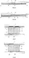
FIG. 3A , the color filter substrate may further comprise aplanarization layer 6; and thefirst sensing electrodes 3 and thesecond sensing electrodes 4 are disposed between theplanarization layer 6 and thetransparent substrate 1, namely are covered by theplanarization layer 6. - As illustrated in
FIG. 3A , theplanarization layer 6 is disposed on thesecond sensing electrodes 4. Theplanarization layer 6 not only can planarize the surface of the film layers on the color filter substrate but also has the insulating function, and can separate a liquid crystal capacitor from a sensing capacitor formed by thefirst sensing electrodes 3 and thesecond sensing electrodes 4 and hence prevent the mutual interference between the liquid crystal capacitor and the sensing capacitor. - Optionally, as illustrated in
FIG. 3B , the color filter substrate may further comprise a transparentconductive layer 7; and theplanarization layer 6 is disposed between the transparentconductive layer 7 and thetransparent substrate 1. - An LCD device displays images by utilization of electric fields to control the light transmittance through liquid crystals. LCD devices can be roughly divided into the vertical electric field driving type and the horizontal electric field driving type according to the direction of an electric field for driving the liquid crystals. The vertical electric field driving type LCD device is that: a common electrode and a pixel electrode are disposed, opposite to each other, on a color filter substrate and an array substrate respectively, and a vertical electric field is formed between the common electrode and the pixel electrode to drive liquid crystals, and for instance includes twist nematic (TN) type and vertical alignment (VA) type LCD devices. The horizontal electric field LCD device is that: a common electrode and a pixel electrode are disposed on an array substrate, and a horizontal electric field is formed between the common electrode and the pixel electrode to drive liquid crystals, and for instance includes advanced super dimensional switching (ADS) type and in-plane switching (IPS) type LCD devices.
- Compared with the horizontal electric field type LCD device, in the vertical electric field type LCD device, a common electrode is also disposed on the color filter substrate, and the vertical electric field is formed by the common electrode and the pixel electrode on the array substrate. In the embodiment of the present invention, the transparent
conductive layer 7 may include a common electrode, and hence the color filter substrate may be applicable to the vertical electric field type LCD device. - In one example, the transparent
conductive layer 7 is disposed on theplanarization layer 6 and includes a common electrode. In a corresponding LCD device, the common electrode on the transparentconductive layer 7 may be electrically connected with a common electrode line on the array substrate. - Moreover, as illustrated in
FIG. 3B , as for the color filter substrate in which the transparentconductive layer 7 includes a common electrode, the color filter substrate may further comprise an insulating layer 8, and the transparentconductive layer 7 is disposed between the insulating layer 8 and thetransparent substrate 1. That is to say, the insulating layer 8 is disposed on the transparentconductive layer 7. As for the color filter substrate in which the transparentconductive layer 7 includes the common electrode, the insulating layer 8 is also disposed on the transparentconductive layer 7 and is configured to prevent the mutual interference between the liquid crystal capacitor and the capacitor formed by thefirst sensing electrode 3 and thesecond sensing electrode 4. - Optionally, as for the color filter substrate of the horizontal electric field type LCD device and an OLED display device, the transparent
conductive layer 7 may also be disposed on theplanarization layer 6, but in this situation the transparentconductive layer 7 is grounded. Therefore, as for the LCD device, the transparentconductive layer 6 may further prevent the mutual interference between the liquid crystal capacitor and the capacitor formed by thefirst sensing electrode 3 and thesecond sensing electrode 4. - The color filter substrate provided by the embodiment of the present invention is not only limited to the color filter substrate as shown in the accompanying drawings, and as long as it falls within the scope of
claim 1. For instance, as illustrated inFIGS. 3A and 3B , thefirst sensing units 31, thesecond sensing units 41 and the second connectinglines 42 may be also disposed beneath the colorfilter film layer 2; the first connectinglines 32 may be disposed on the colorfilter film layer 2; throughholes 22 are formed in the colorfilter film layer 2, and the first connectinglines 32 are electrically connected with thefirst sensing units 31 via the through holes 22. - In another example not according to the invention, as illustrated in
FIG. 4 andFIG. 6A or FIG. 6B , thefirst sensing units 31 and the first connectinglines 32 are arranged on a same layer; thesecond sensing units 41 and the second connectinglines 42 are arranged on a same layer; thefirst sensing units 31 and thesecond sensing units 41 are arranged on different layers. The colorfilter film layer 2 is disposed between thefirst sensing electrode 3 and thesecond sensing electrode 4, so that thefirst sensing electrode 3 is insulated from thesecond sensing electrode 4. As illustrated inFIG. 4 , thefirst sensing units 31 and the first connectinglines 32 are arranged on a same layer, so that thefirst sensing units 31, disposed in the same row, of thefirst sensing electrode 3 can be directly connected with each other through the first connectinglines 32; thesecond sensing units 41 and the second connectinglines 42 are arranged on a same layer, so that thesecond sensing units 41, disposed in the same row, of thesecond sensing electrode 4 can be directly connected with each other through the second connectinglines 42. The colorfilter film layer 2 is disposed between thefirst sensing electrode 3 and thesecond sensing electrode 4, so that thefirst sensing electrode 3 is insulated from thesecond sensing electrode 4. - Optionally, as illustrated in
FIG. 6A , the color filter substrate may further comprise: a black matrix (BM)layer 5 disposed between the colorfilter film layer 2 and thetransparent substrate 1. TheBM layer 5 includes BMs which are disposed at the connected
positions of thefilter elements 21 of the color filter film layer. For instance, as illustrated inFIG. 6 , theBM layer 5 is disposed beneath thefirst sensing electrode 3. The colorfilter film layer 2 includes a plurality of thefilter elements 21; joints are provided at the connected positions of thefilter elements 21; and the BMs include staggered black strips and are disposed at the connected positions of thefilter elements 21 of the color filter film layer. Therefore, the phenomenon of light leakage at the connected positions of thefilter elements 21 in the colorfilter film layer 2 can be further prevented. - Optionally, as illustrated in
FIG. 6A , the color filter substrate may further comprise aplanarization layer 6; and the colorfilter film layer 2, thefirst sensing electrode 3 and thesecond sensing electrode 4 are disposed between theplanarization layer 6 and thetransparent substrate 1, namely are covered by theplanarization layer 6. - As illustrated in
FIG. 6A , theplanarization layer 6 is disposed on thesecond sensing electrode 4. Theplanarization layer 6 not only can planarize the surface of the film layers on the color filter substrate but also has the insulating function, and can separate the liquid crystal capacitor from the sensing capacitor formed by thefirst sensing electrode 3 and thesecond sensing electrode 4 and hence prevent the mutual interference between the liquid crystal capacitance and the sensing capacitance. - Optionally, as illustrated in
FIG. 6B , the color filter substrate may further comprise a transparentconductive layer 7; and theplanarization layer 6 is disposed between the transparentconductive layer 7 and thetransparent substrate 1. - Compared with the horizontal electric field type LCD device, in the vertical electric field type LCD device, the color filter substrate is also provided with a common electrode; and a vertical electric field is formed by the common electrode and the pixel electrode on the array substrate. In the example not according to the invention, the transparent conductive layer may include a common electrode, and hence the color filter substrate may be applicable to the vertical electric field type LCD device.
- The transparent conductive layer is disposed on the
planarization layer 6. The transparentconductive layer 7 includes a common electrode. In the LCD device, the common electrode of the transparentconductive layer 7 may be electrically connected with the common electrode line on the array substrate. - Moreover, as illustrated in
FIG. 6B , as for the color filter substrate in which the transparentconductive layer 7 includes a common electrode, the color filter substrate may further comprise an insulating layer 8, and the transparentconductive layer 7 is disposed between the insulating layer 8 and thetransparent substrate 1. That is to say, the insulating layer 8 is disposed on the transparentconductive layer 7. As for the color filter substrate in which the transparentconductive layer 7 includes the common electrode, the insulating layer 8 is also disposed on the transparentconductive layer 7 and configured to prevent the mutual interference between the liquid crystal capacitor and the capacitor formed by thefirst sensing electrode 3 and thesecond sensing electrode 4. - Optionally, as for the color filter substrate of the horizontal electric field type LCD device and the OLED display device, the transparent
conductive layer 7 may be also disposed on theplanarization layer 6, but in this situation the transparent conductive layer is grounded. Therefore, as for the LCD device, the transparentconductive layer 7 is equivalent to the insulating layer and can further prevent the mutual interference between the liquid crystal capacitor and the capacitor formed by thefirst sensing electrode 3 and thesecond sensing electrode 4. - The color filter substrate is not limited to the color filter substrate as shown in the accompanying drawings, and as long as the
first sensing electrodes 3 and thesecond sensing electrodes 4 are insulated from each other through the colorfilter film layer 2, it falls within the scope of protection of the present invention. For instance, as illustrated inFIGs. 6A and 6B , theBM layer 5 may also be disposed between thefirst sensing electrode 3 and the colorfilter film layer 2. - An embodiment of the present invention provides a touch screen, which comprises any of the color filter substrates provided by the embodiments of the present invention. In order to achieve the touch function of the touch screen, the touch screen further comprises drive circuits (not shown) which are connected with the
first sensing electrodes 3 and thesecond sensing electrodes 4 and configured to control thefirst sensing electrodes 3 and thesecond sensing electrodes 4. The touch screen is applicable to an LCD device and also applicable to an OLED display device. - It should be noted that the
first sensing electrodes 3 and thesecond sensing electrodes 4 are connected with the drive circuits for controlling thefirst sensing electrodes 3 and thesecond sensing electrodes 4 on edges of the color filter substrate. - An LCD device generally comprises an array substrate and a color filter substrate which are arranged opposite to each other to form a liquid crystal cell; and a drive circuit is usually disposed on the array substrate. Preferably, the drive circuits for controlling the
first sensing electrodes 3 and thesecond sensing electrodes 4 can be arranged together with the drive circuits on the array substrate. Therefore, not only the processes can be reduced but also the integration level of the display device can be improved. Moreover, the number of circuit boards can be reduced and the costs can be reduced as well. In this case, thefirst sensing electrodes 3 and thesecond sensing electrodes 4 on the color filter substrate must be transferred to the array substrate. - In one embodiment, as illustrated in the sectional views of
FIG. 7 and in the example not according to invention as illustrated inFig. 8 , thefirst sensing electrode 3 and thesecond sensing electrode 4 are electrically connected with connection points 21 on thearray substrate 20 through an anisotropicconductive material 10 and connected with the drive circuits and the like through the connection points 21. The anisotropicconductive material 10 is separated from each other through an insulatingsealant 11. The anisotropic conductive material may be anisotropic conductive adhesive (ACA) containing conductive metal balls. - An embodiment of the present invention provides a display device, which comprises any touch screen provided by the embodiment of the present invention. The display device may be a display device such as an LCD, electronic paper and an OLED display or any product or component including the display device and having the display function such as a television, a digital camera, a mobile phone and a tablet PC.
- An embodiment of the present invention provides a method for manufacturing a color filter substrate. As illustrated in
FIG. 9 , the method comprises the following steps. - Step S101: providing first connecting lines on a transparent substrate.
- For instance, the first connecting lines are configured to electrically connect first sensing units disposed in the same row. Moreover, preferably, as illustrated in
FIG. 10 , the first connectinglines 32 are in the shape of black strips and disposed at connected positions of filter elements of a color filter film layer to be formed later and hence can further prevent the phenomenon of light leakage at the connected positions of the filter elements of the color filter film layer. Thetransparent substrate 1 is, for instance, a glass substrate, a plastic substrate and the like. - Step S102: providing a color filter film layer on the transparent substrate.
- For instance, the color filter film layer includes a plurality of closely connected filter elements. Moreover, preferably, an overlapped portion is disposed on edges of two adjacent filter elements of the color filter film layer, and hence the phenomenon of light leakage due to the fact that the two adjacent filter elements are not closely connected can be prevented. As illustrated in
FIG. 11 , throughholes 22 are formed in the colorfilter film layer 2. It should be noted that the step S102 is executed after the step S101, and hence the process of providing the colorfilter film layer 2 on thetransparent substrate 1 is equivalent to the process of providing the colorfilter film layer 2 on thetransparent substrate 1 on which the first connectinglines 32 formed in the step S101 are formed. - Step S103: providing first sensing units, second sensing units and second connecting lines on the transparent substrate.
- For instance, as illustrated in
FIG. 12 , thefirst sensing units 31 disposed in the same row are electrically connected with the first connectinglines 32 via the throughholes 22 in the colorfilter film layer 2. The second connectinglines 42 are configured to electrically connect thesecond sensing units 41 disposed in the same row. It should be noted that the step S103 is executed after the steps S101 and S102, and hence the process of providing thefirst sensing units 31, thesecond sensing units 41 and the second connectinglines 42 on thetransparent substrate 1 is equivalent to the process of providing thefirst sensing units 31, thesecond sensing units 41 and the second connectinglines 42 on thetransparent substrate 1 on which the first connectinglines 32 formed in the step S101 and the colorfilter film layer 2 formed in the step S102 are formed. Similarly, in subsequent steps, the transparent substrate includes film or layer structures formed in the previous steps. - Optionally, the method may further comprise: providing black strips which are intercrossed with the first connecting
lines 32 on thetransparent substrate 1. For instance, the black strips are disposed at the connected positions of the filter elements of the color filter film layer and insulated from the first connecting lines. Optionally, the black strips and the first connecting lines may be arranged on different layers. For instance, the step of providing the black strips may be executed after the step S104. Or, the step of providing the black strips may be executed between the step S101 and the step S102. Or, the black strips are arranged on a same layer with the first connecting lines and are not connected with the first connecting lines so as to be insulated from the first connecting lines. - Optionally, the manufacturing method may further comprise step S104: providing a planarization layer on the transparent substrate.
- For instance, as illustrated in
FIG. 3A or 3B , the colorfilter film layer 2, thefirst sensing electrode 3 and thesecond sensing electrode 4 are disposed between theplanarization layer 6 and thetransparent substrate 1. Theplanarization layer 6 not only can planarize the surface of the film layers on the color filter substrate but also has the insulating function, and can separate the liquid crystal capacitance from the sensing capacitance formed by thefirst sensing electrode 3 and thesecond sensing electrode 4 and hence prevent the mutual interference between the liquid crystal capacitor and the sensing capacitor. - Optionally, the manufacturing method may further comprise step S105: providing a transparent conductive layer on the transparent substrate.
- For instance, the planarization layer is disposed between the transparent conductive layer and the transparent substrate. As for the horizontal electric field type LCD device, the transparent conductive layer of the color filter substrate is grounded, and hence the transparent conductive layer can further prevent the mutual interference between the liquid crystal capacitor and the capacitor formed by the first sensing electrode and the second sensing electrode. As for the vertical electric field type LCD device, the transparent conductive layer on the color filter substrate includes a common electrode. As for the VA type LCD device, the method for manufacturing the color filter substrate further comprises the step of providing an insulating layer on the transparent substrate.
- For instance, the transparent conductive layer is disposed between the insulating layer and the transparent substrate. The insulating layer is configured to prevent the mutual interference between the liquid crystal capacitor and the capacitor formed by the first sensing electrode and the second sensing electrode.
- Of course, the method for manufacturing the color filter substrate provided by the embodiment of the present invention is not only limited to the above steps. For instance, the step of providing the black strips which are intercrossed with the first connecting lines on the transparent substrate may also be executed after the step S103.
- Another example not according to the present invention provides a method for manufacturing a color filter substrate. As illustrated in
FIG. 13 , the method comprises the following steps. - Step S201: providing first sensing units and first connecting lines on a transparent substrate.
- For instance, as illustrated in
FIGs. 4 and15 , the first connectinglines 32 are configured to electrically connect thefirst sensing units 31 disposed in the same row. Thetransparent substrate 1 is, for instance, a glass substrate, a plastic substrate and the like. - Step S202: providing a color filter film layer on the transparent substrate.
- For instance, as illustrated in
FIGs. 4 and16 , the colorfilter film layer 2 includes a plurality of filter elements. Preferably, an overlapped portion is disposed on edge portions of two adjacent filter elements of the color filter film layer, and hence the phenomenon of light leakage due to the fact that the two adjacent filter elements are not closely connected can be prevented. It should be noted that the step S202 is executed after the step S201, and hence the process of providing the colorfilter film layer 2 on thetransparent substrate 1 is equivalent to the process of providing the colorfilter film layer 2 on thetransparent substrate 1 on which thefirst sensing units 31 and the first connectinglines 32 formed in the step S201 are formed. - Step S203: providing second sensing units and second connecting lines on the transparent substrate.
- For instance, as illustrated in
FIGs. 4 and17 , the second connectinglines 42 are configured to electrically connect thesecond sensing units 41 disposed in the same row. It should be noted that the step S203 is executed after the steps S201 and S202, and hence the process of providing the second sensing units and the second connecting lines on the transparent substrate is equivalent to the process of providing thesecond sensing units 41 and the second connectinglines 42 on thetransparent substrate 1 on which thefirst sensing units 31 and the first connectinglines 32 formed in the step S201 and the colorfilter film layer 2 formed in the step S202 are formed. - Optionally, the manufacturing method may further comprise step S205 before the step S201: providing a
BM layer 5 on the transparent substrate, as illustrated inFIG. 14 . - For instance, the BM layer includes BMs which are disposed at the connected positions of the filter elements of the color filter film layer. The BMs are configured to further prevent the phenomenon of light leakage at the connected positions of the filter elements of the color filter film layer.
- Optionally, the manufacturing method may further comprise step S204: providing a planarization layer on the transparent substrate.
- For instance, as illustrated in
FIGs. 6A and 6B , the colorfilter film layer 2, thefirst sensing electrode 3 and thesecond sensing electrode 4 are disposed between theplanarization layer 6 and thetransparent substrate 1. Theplanarization layer 6 not only can planarize the surface of the film layers on the substrate but also has the insulating function and can separate the liquid crystal capacitance and the sensing capacitance formed by thefirst sensing electrode 3 and thesecond sensing electrode 4 and hence can prevent the mutual interference between the liquid crystal capacitor and the sensing capacitor. - Optionally, the manufacturing method may further comprise step S206: providing a transparent conductive layer on the transparent substrate.
- For instance, the planarization layer is disposed between the transparent conductive layer and the transparent substrate. As for the horizontal electric field type LCD device, the transparent conductive layer of the color filter substrate is grounded, and hence the transparent conductive layer can further prevent the mutual interference between the liquid crystal capacitor and the capacitor formed by the first sensing electrode and the second sensing electrode. As for the vertical electric field type LCD device, the transparent conductive layer on the color filter substrate includes: a common electrode which is electrically connected with a common electrode line on an array substrate. Moreover, as for the VA type LCD device, the method for manufacturing the color filter substrate further comprises the step of providing an insulating layer on the transparent substrate.
- For instance, the transparent conductive layer is disposed between the insulating layer and the transparent substrate. The insulating layer is configured to prevent the mutual interference between the liquid crystal capacitor and the capacitor formed by the
first sensing electrode 3 and thesecond sensing electrode 4. - Of course, the manufacturing method provided by the example not according to the present invention is not only limited to the above steps. For instance, the step of providing the BM layer on the transparent substrate may also be executed after the step S203.
Claims (10)
- A color filter substrate, comprising:a transparent substrate (1) and a color filter film layer (2) disposed on the transparent substrate (1), wherein the color filter film layer (2) includes a plurality of filter elements (21), a plurality of first sensing electrodes (3) and a plurality of second sensing electrodes (4);wherein the first sensing electrodes (3) are insulated from the second sensing electrodes (4) at crossed positions by portions of the color filter film layer (2), disposed at the crossed positions of the first sensing electrodes (3) and the second sensing electrodes (4), in order to form a touch sensing capacitor;the first sensing electrodes (3) include:
first sensing units (31) and first connecting lines (32), in which the first sensing units (31) of a same first sensing electrode are electrically connected with each other through the first connecting lines (32); the first connecting lines (32) are part of a black matrix, and the first connecting lines (32) are disposed at connecting positions of the filter elements (21) of the color filter film layer (2); characterized in thatthe second sensing electrodes (4) include: second sensing units (41) and second connecting lines (42), in which the second sensing units (41) of a same second sensing electrode (4) are electrically connected with each other through the second connecting lines (42);the first sensing units (31), the second sensing units (41) and the second connecting lines (42) are arranged on a same layer; the first sensing units (31) are insulated from the second sensing units (41) and the second connecting lines (42); the first connecting lines (32) and the first sensing units (31) are arranged on different layers; the color filter film layer (2) is disposed between the first connecting lines (32) and the first sensing units (31); through holes (22) are formed in the color filter film layer (2); and the first sensing units (31) of a same first sensing electrode are electrically connected with the first connecting lines (32) via the through holes (22). - The color filter substrate according to claim 1, wherein a plurality of the first sensing electrodes (3) are arranged in a plurality of rows along a first direction; and a plurality of the second sensing electrodes (4) are arranged in a plurality of rows along a second direction.
- The color filter substrate according to claim 1, further comprising black strips which are intersected with the first connecting lines (32), wherein the black strips are disposed at the connected positions of the filter elements (21) of the color filter film layer (2) and insulated from the first connecting lines (32).
- The color filter substrate according to any one of claims 1 to 3, further comprising a planarization layer (6), wherein the color filter film layer (2), the first sensing electrodes (3) and the second sensing electrodes (4) are disposed between the planarization layer (6) and the transparent substrate (1).
- The color filter substrate according to claim 4, further comprising a transparent conductive layer, wherein the planarization layer (6) is disposed between the transparent conductive layer and the transparent substrate (1).
- The color filter substrate according to claim 5, wherein the transparent conductive layer is configured to be grounded.
- A touch screen, comprising the color filter substrate according to any one of claims 1 to 6.
- The touch screen according to claim 7, further comprising: an array substrate and drive circuits which are connected with the first sensing electrodes (3) and the second sensing electrodes (4) and configured to control the first sensing electrodes (3) and the second sensing electrodes (4), wherein the driving circuits are arranged together with a drive circuit on the array substrate.
- A display device, comprising the touch screen according to claim 7 or 8.
- A method for manufacturing a color filter substrate according to claim 1, comprising:providing first connecting lines (32) on a transparent substrate (1), in which the first connecting lines (32) are configured to electrically connect first sensing units (31) of a same first sensing electrode;providing a color filter film layer (2) on the transparent substrate (1), in which the color filter film layer (2) includes a plurality of closely connected filter elements (21), and through holes (22) are formed in the color filter film layer (2); andproviding the first sensing units (31), second sensing units (41) and second connecting lines (42) on the transparent substrate (1), in which the first sensing units (31) are electrically connected with the first connecting lines (32) via the through holes (22) in the color filter film layer (2); the second connecting lines (42) are configured to electrically connect the second sensing units (41) of a same second sensing electrode; and the first sensing units (31) are insulated from the second sensing units (41) and the second connecting lines (42), whereinthe first connecting lines (32) are part of a black matrix, andthe first connecting lines (32) are disposed at connected positions of the filter elements (21) of the color filter film layer (2).
Applications Claiming Priority (2)
| Application Number | Priority Date | Filing Date | Title |
|---|---|---|---|
| CN201310098751.7A CN103197463B (en) | 2013-03-26 | 2013-03-26 | Color film substrate and production method, touch screen and display device thereof |
| PCT/CN2013/077421 WO2014153855A1 (en) | 2013-03-26 | 2013-06-18 | Colour film substrate and manufacturing method therefor, touchscreen and display device |
Publications (3)
| Publication Number | Publication Date |
|---|---|
| EP2980635A1 EP2980635A1 (en) | 2016-02-03 |
| EP2980635A4 EP2980635A4 (en) | 2016-12-07 |
| EP2980635B1 true EP2980635B1 (en) | 2019-01-30 |
Family
ID=48720136
Family Applications (1)
| Application Number | Title | Priority Date | Filing Date |
|---|---|---|---|
| EP13834319.9A Active EP2980635B1 (en) | 2013-03-26 | 2013-06-18 | Colour film substrate and manufacturing method therefor, touchscreen and display device |
Country Status (4)
| Country | Link |
|---|---|
| US (1) | US20160188070A1 (en) |
| EP (1) | EP2980635B1 (en) |
| CN (1) | CN103197463B (en) |
| WO (1) | WO2014153855A1 (en) |
Families Citing this family (11)
| Publication number | Priority date | Publication date | Assignee | Title |
|---|---|---|---|---|
| CN103618954A (en) * | 2013-11-05 | 2014-03-05 | 苏州三星电子电脑有限公司 | Display system control device and control method |
| CN104951156A (en) * | 2014-03-31 | 2015-09-30 | 宸盛光电有限公司 | Capacitive touch control device |
| CN104166481B (en) | 2014-08-15 | 2017-05-24 | 京东方科技集团股份有限公司 | Display substrate and display device |
| CN104777932A (en) * | 2015-04-01 | 2015-07-15 | 深圳市华星光电技术有限公司 | Touch control liquid crystal display and touch control liquid crystal panel thereof |
| CN104731414B (en) * | 2015-04-07 | 2019-01-11 | 武汉华星光电技术有限公司 | Touch control display apparatus and electronic equipment |
| CN106066720B (en) * | 2015-04-22 | 2019-04-26 | 财团法人工业技术研究院 | Induction device |
| CN105068295B (en) * | 2015-09-11 | 2018-02-16 | 京东方科技集团股份有限公司 | A kind of touch-control display panel and preparation method thereof, touch control display apparatus |
| CN105717685A (en) * | 2016-04-13 | 2016-06-29 | 京东方科技集团股份有限公司 | Cassette aligning substrate, preparation method thereof and touch display panel |
| CN205723639U (en) | 2016-04-19 | 2016-11-23 | 鄂尔多斯市源盛光电有限责任公司 | A kind of sealed plastic box structure, display floater and display device |
| CN106775125A (en) * | 2017-01-20 | 2017-05-31 | 京东方科技集团股份有限公司 | Color membrane substrates and preparation method thereof, touch-screen |
| CN113410709B (en) * | 2018-06-29 | 2022-09-16 | 华为技术有限公司 | Mobile terminal |
Family Cites Families (36)
| Publication number | Priority date | Publication date | Assignee | Title |
|---|---|---|---|---|
| US7641688B2 (en) * | 2004-09-16 | 2010-01-05 | Evera Medical, Inc. | Tissue augmentation device |
| JP2008032756A (en) * | 2004-11-17 | 2008-02-14 | Sharp Corp | Touch panel display device and touch panel |
| TWI367437B (en) * | 2007-09-29 | 2012-07-01 | Au Optronics Corp | Touch panel and manufacturing method thereof |
| US7924350B2 (en) * | 2007-10-12 | 2011-04-12 | Au Optronics Corporation | Capacitance type touch panel |
| US8134540B2 (en) * | 2007-10-16 | 2012-03-13 | Wintek Corporation | Touch panel and liquid crystal display panel |
| KR20090066459A (en) * | 2007-12-20 | 2009-06-24 | 삼성전자주식회사 | Color filter substrate of liquid crystal display device and method for manufacturing the same |
| TWI389020B (en) * | 2008-03-25 | 2013-03-11 | Elan Microelectronics | Touch panel device |
| TWI393924B (en) * | 2008-06-25 | 2013-04-21 | Au Optronics Corp | Touch display panel, color filter of and fabricating method thereof |
| CN101320107B (en) * | 2008-07-04 | 2010-04-21 | 友达光电股份有限公司 | Touch control type display panel, colorful color filter and its production method |
| US20100007627A1 (en) * | 2008-07-09 | 2010-01-14 | Chi Hsin Electronics Corp. | Touch signal transmission circuit and liquid crystal display using the same |
| TWI377497B (en) * | 2008-11-05 | 2012-11-21 | Au Optronics Corp | Touch-sensing substrate, color filter substrate and touch-sensing liquid crystal display |
| TWI376623B (en) * | 2008-11-19 | 2012-11-11 | Au Optronics Corp | Touch panel and touch display panel |
| TWI380089B (en) * | 2008-12-03 | 2012-12-21 | Au Optronics Corp | Method of forming a color filter touch sensing substrate |
| TWI374299B (en) * | 2008-12-11 | 2012-10-11 | Au Optronics Corp | Color filter touch sensing substrate and display panel and manufacturing methods of the same |
| CN101819343B (en) * | 2008-12-23 | 2011-08-31 | 友达光电股份有限公司 | Colored light-filtering touch base plate, display panel and manufacturing methods thereof |
| CN101963713A (en) * | 2009-07-24 | 2011-02-02 | 宸鸿光电科技股份有限公司 | plane switching liquid crystal display (IPSLCD) with touch control function |
| KR101309862B1 (en) * | 2009-12-10 | 2013-09-16 | 엘지디스플레이 주식회사 | Liquid Crystal Display Device Including Touch Panel |
| US8593413B2 (en) * | 2010-03-01 | 2013-11-26 | Cando Corporation | Sensory structure of capacitive touch panel and capacitive touch panel having the same |
| KR20110121662A (en) * | 2010-08-03 | 2011-11-08 | 삼성전기주식회사 | Touch panel and a manufacturing method the same |
| US9703425B2 (en) * | 2010-09-01 | 2017-07-11 | G2Touch Co., Ltd. | Capacitive touch detecting device and method using level shift, and display device using the same |
| TWI423092B (en) * | 2010-10-04 | 2014-01-11 | Au Optronics Corp | Touch panel and repairing method thereof |
| US20130222317A1 (en) * | 2010-10-08 | 2013-08-29 | Sharp Kabushiki Kaisha | Display device, and process for manufacturing display device |
| KR101230196B1 (en) * | 2010-10-29 | 2013-02-06 | 삼성디스플레이 주식회사 | Liquid Crystal Display having a Touch Screen Panel |
| US8804056B2 (en) * | 2010-12-22 | 2014-08-12 | Apple Inc. | Integrated touch screens |
| US10088930B2 (en) * | 2011-11-25 | 2018-10-02 | Shanghai Tianma Micro-electronics Co., Ltd. | Active matrix organic light emitting diode in-cell touch panel and drive method thereof |
| CN102566116A (en) * | 2012-02-13 | 2012-07-11 | 友达光电股份有限公司 | Capacitance type touch display panel |
| TWI476459B (en) * | 2012-05-03 | 2015-03-11 | Innocom Tech Shenzhen Co Ltd | A color filter substrate, and a touch screen display device |
| TWM445719U (en) * | 2012-05-22 | 2013-01-21 | Inv Element Inc | Embedded touch display panel structure with metal induction layer |
| CN102749766A (en) * | 2012-06-18 | 2012-10-24 | 北京京东方光电科技有限公司 | Touch display panel and displayer |
| TWI566153B (en) * | 2012-07-10 | 2017-01-11 | 元太科技工業股份有限公司 | Touch panel and manufacturing method thereof and touch display panel |
| JP6050728B2 (en) * | 2012-07-24 | 2016-12-21 | 株式会社ジャパンディスプレイ | Liquid crystal display device with touch sensor and electronic device |
| JP5968275B2 (en) * | 2012-08-07 | 2016-08-10 | 株式会社ジャパンディスプレイ | Display device with touch sensor and electronic device |
| CN104620211A (en) * | 2012-09-14 | 2015-05-13 | 夏普株式会社 | Touch panel and touch panel integrated display device |
| US9244559B2 (en) * | 2012-12-14 | 2016-01-26 | Atmel Corporation | Integrated pixel display and touch sensor |
| CN103914163B (en) * | 2012-12-31 | 2017-05-17 | 上海天马微电子有限公司 | Touch panel and touch display device |
| TWM459453U (en) * | 2013-01-10 | 2013-08-11 | Inv Element Inc | In-cell touch display panel structure with metal sensing layer on lower substrate |
-
2013
- 2013-03-26 CN CN201310098751.7A patent/CN103197463B/en active Active
- 2013-06-18 EP EP13834319.9A patent/EP2980635B1/en active Active
- 2013-06-18 WO PCT/CN2013/077421 patent/WO2014153855A1/en active Application Filing
- 2013-06-18 US US14/344,563 patent/US20160188070A1/en not_active Abandoned
Non-Patent Citations (1)
| Title |
|---|
| None * |
Also Published As
| Publication number | Publication date |
|---|---|
| US20160188070A1 (en) | 2016-06-30 |
| WO2014153855A1 (en) | 2014-10-02 |
| CN103197463B (en) | 2015-06-17 |
| CN103197463A (en) | 2013-07-10 |
| EP2980635A4 (en) | 2016-12-07 |
| EP2980635A1 (en) | 2016-02-03 |
Similar Documents
| Publication | Publication Date | Title |
|---|---|---|
| EP2980635B1 (en) | Colour film substrate and manufacturing method therefor, touchscreen and display device | |
| JP7023904B2 (en) | Display device including touch sensor | |
| US10871839B2 (en) | Color filter substrate, array substrate and display device | |
| US9665222B2 (en) | In-cell touch panel and display device with self-capacitance electrodes | |
| US9057906B2 (en) | Capacitive touch screens, method of driving the same and displays | |
| CN102081247B (en) | Display device with a touch device | |
| KR101609485B1 (en) | Capacitive in-cell touch panel and display device | |
| US8878814B2 (en) | Liquid crystal display device provided with a sensing electrode for sensing a touch of a user | |
| US8964132B2 (en) | Color filter substrate and capacitive touch screen | |
| CN103294312B (en) | Capacitive touch screen, capacitive touch screen preparation method and display device | |
| US20120086654A1 (en) | Liquid Crystal Display Device | |
| CN103226423A (en) | Embedded type capacitor touch display panel, display device, control device and method | |
| US20150029144A1 (en) | Display device | |
| US10649562B2 (en) | In-cell touch screen and a display device | |
| TWI485599B (en) | Touch component and flat panel display | |
| KR20160053251A (en) | In Cell Touch Liquid Crystal Display Device And Method of Manufacturing The same, And Method of Manufacturing Thin Film Transistor Array Substrate And Color Filter Array Substrate | |
| KR20100095400A (en) | Capacitive touch panel | |
| CN102135824B (en) | Built-in touch display and processing method thereof | |
| CN105528127A (en) | In-cell touch panel and trace layout thereof | |
| WO2013189140A1 (en) | Touch display panel and display | |
| US9194985B1 (en) | Color filter substrate, manufacturing method thereof, and display panel | |
| US20160162072A1 (en) | Touch panel, manufacturing method thereof and display device | |
| US9019221B2 (en) | Display device integrated with touch screen panel | |
| CN203705776U (en) | Touch control structure of liquid crystal display panel | |
| US20180299998A1 (en) | In-cell touch display panels and electronic devices |
Legal Events
| Date | Code | Title | Description |
|---|---|---|---|
| PUAI | Public reference made under article 153(3) epc to a published international application that has entered the european phase |
Free format text: ORIGINAL CODE: 0009012 |
|
| 17P | Request for examination filed |
Effective date: 20140310 |
|
| AK | Designated contracting states |
Kind code of ref document: A1 Designated state(s): AL AT BE BG CH CY CZ DE DK EE ES FI FR GB GR HR HU IE IS IT LI LT LU LV MC MK MT NL NO PL PT RO RS SE SI SK SM TR |
|
| AX | Request for extension of the european patent |
Extension state: BA ME |
|
| DAX | Request for extension of the european patent (deleted) | ||
| A4 | Supplementary search report drawn up and despatched |
Effective date: 20161108 |
|
| RIC1 | Information provided on ipc code assigned before grant |
Ipc: G02F 1/1335 20060101AFI20161102BHEP Ipc: G06F 3/041 20060101ALI20161102BHEP Ipc: G02F 1/1343 20060101ALI20161102BHEP Ipc: G02F 1/1333 20060101ALI20161102BHEP |
|
| STAA | Information on the status of an ep patent application or granted ep patent |
Free format text: STATUS: EXAMINATION IS IN PROGRESS |
|
| 17Q | First examination report despatched |
Effective date: 20171212 |
|
| GRAP | Despatch of communication of intention to grant a patent |
Free format text: ORIGINAL CODE: EPIDOSNIGR1 |
|
| STAA | Information on the status of an ep patent application or granted ep patent |
Free format text: STATUS: GRANT OF PATENT IS INTENDED |
|
| INTG | Intention to grant announced |
Effective date: 20180815 |
|
| GRAS | Grant fee paid |
Free format text: ORIGINAL CODE: EPIDOSNIGR3 |
|
| GRAA | (expected) grant |
Free format text: ORIGINAL CODE: 0009210 |
|
| STAA | Information on the status of an ep patent application or granted ep patent |
Free format text: STATUS: THE PATENT HAS BEEN GRANTED |
|
| AK | Designated contracting states |
Kind code of ref document: B1 Designated state(s): AL AT BE BG CH CY CZ DE DK EE ES FI FR GB GR HR HU IE IS IT LI LT LU LV MC MK MT NL NO PL PT RO RS SE SI SK SM TR |
|
| REG | Reference to a national code |
Ref country code: GB Ref legal event code: FG4D |
|
| REG | Reference to a national code |
Ref country code: CH Ref legal event code: EP |
|
| REG | Reference to a national code |
Ref country code: AT Ref legal event code: REF Ref document number: 1093732 Country of ref document: AT Kind code of ref document: T Effective date: 20190215 |
|
| REG | Reference to a national code |
Ref country code: IE Ref legal event code: FG4D |
|
| REG | Reference to a national code |
Ref country code: DE Ref legal event code: R096 Ref document number: 602013050342 Country of ref document: DE |
|
| REG | Reference to a national code |
Ref country code: NL Ref legal event code: FP |
|
| REG | Reference to a national code |
Ref country code: LT Ref legal event code: MG4D |
|
| PG25 | Lapsed in a contracting state [announced via postgrant information from national office to epo] |
Ref country code: NO Free format text: LAPSE BECAUSE OF FAILURE TO SUBMIT A TRANSLATION OF THE DESCRIPTION OR TO PAY THE FEE WITHIN THE PRESCRIBED TIME-LIMIT Effective date: 20190430 Ref country code: FI Free format text: LAPSE BECAUSE OF FAILURE TO SUBMIT A TRANSLATION OF THE DESCRIPTION OR TO PAY THE FEE WITHIN THE PRESCRIBED TIME-LIMIT Effective date: 20190130 Ref country code: LT Free format text: LAPSE BECAUSE OF FAILURE TO SUBMIT A TRANSLATION OF THE DESCRIPTION OR TO PAY THE FEE WITHIN THE PRESCRIBED TIME-LIMIT Effective date: 20190130 Ref country code: SE Free format text: LAPSE BECAUSE OF FAILURE TO SUBMIT A TRANSLATION OF THE DESCRIPTION OR TO PAY THE FEE WITHIN THE PRESCRIBED TIME-LIMIT Effective date: 20190130 Ref country code: PL Free format text: LAPSE BECAUSE OF FAILURE TO SUBMIT A TRANSLATION OF THE DESCRIPTION OR TO PAY THE FEE WITHIN THE PRESCRIBED TIME-LIMIT Effective date: 20190130 Ref country code: PT Free format text: LAPSE BECAUSE OF FAILURE TO SUBMIT A TRANSLATION OF THE DESCRIPTION OR TO PAY THE FEE WITHIN THE PRESCRIBED TIME-LIMIT Effective date: 20190530 Ref country code: ES Free format text: LAPSE BECAUSE OF FAILURE TO SUBMIT A TRANSLATION OF THE DESCRIPTION OR TO PAY THE FEE WITHIN THE PRESCRIBED TIME-LIMIT Effective date: 20190130 |
|
| REG | Reference to a national code |
Ref country code: AT Ref legal event code: MK05 Ref document number: 1093732 Country of ref document: AT Kind code of ref document: T Effective date: 20190130 |
|
| PG25 | Lapsed in a contracting state [announced via postgrant information from national office to epo] |
Ref country code: GR Free format text: LAPSE BECAUSE OF FAILURE TO SUBMIT A TRANSLATION OF THE DESCRIPTION OR TO PAY THE FEE WITHIN THE PRESCRIBED TIME-LIMIT Effective date: 20190501 Ref country code: BG Free format text: LAPSE BECAUSE OF FAILURE TO SUBMIT A TRANSLATION OF THE DESCRIPTION OR TO PAY THE FEE WITHIN THE PRESCRIBED TIME-LIMIT Effective date: 20190430 Ref country code: RS Free format text: LAPSE BECAUSE OF FAILURE TO SUBMIT A TRANSLATION OF THE DESCRIPTION OR TO PAY THE FEE WITHIN THE PRESCRIBED TIME-LIMIT Effective date: 20190130 Ref country code: IS Free format text: LAPSE BECAUSE OF FAILURE TO SUBMIT A TRANSLATION OF THE DESCRIPTION OR TO PAY THE FEE WITHIN THE PRESCRIBED TIME-LIMIT Effective date: 20190530 Ref country code: LV Free format text: LAPSE BECAUSE OF FAILURE TO SUBMIT A TRANSLATION OF THE DESCRIPTION OR TO PAY THE FEE WITHIN THE PRESCRIBED TIME-LIMIT Effective date: 20190130 Ref country code: HR Free format text: LAPSE BECAUSE OF FAILURE TO SUBMIT A TRANSLATION OF THE DESCRIPTION OR TO PAY THE FEE WITHIN THE PRESCRIBED TIME-LIMIT Effective date: 20190130 |
|
| PG25 | Lapsed in a contracting state [announced via postgrant information from national office to epo] |
Ref country code: EE Free format text: LAPSE BECAUSE OF FAILURE TO SUBMIT A TRANSLATION OF THE DESCRIPTION OR TO PAY THE FEE WITHIN THE PRESCRIBED TIME-LIMIT Effective date: 20190130 Ref country code: AL Free format text: LAPSE BECAUSE OF FAILURE TO SUBMIT A TRANSLATION OF THE DESCRIPTION OR TO PAY THE FEE WITHIN THE PRESCRIBED TIME-LIMIT Effective date: 20190130 Ref country code: DK Free format text: LAPSE BECAUSE OF FAILURE TO SUBMIT A TRANSLATION OF THE DESCRIPTION OR TO PAY THE FEE WITHIN THE PRESCRIBED TIME-LIMIT Effective date: 20190130 Ref country code: SK Free format text: LAPSE BECAUSE OF FAILURE TO SUBMIT A TRANSLATION OF THE DESCRIPTION OR TO PAY THE FEE WITHIN THE PRESCRIBED TIME-LIMIT Effective date: 20190130 Ref country code: IT Free format text: LAPSE BECAUSE OF FAILURE TO SUBMIT A TRANSLATION OF THE DESCRIPTION OR TO PAY THE FEE WITHIN THE PRESCRIBED TIME-LIMIT Effective date: 20190130 Ref country code: RO Free format text: LAPSE BECAUSE OF FAILURE TO SUBMIT A TRANSLATION OF THE DESCRIPTION OR TO PAY THE FEE WITHIN THE PRESCRIBED TIME-LIMIT Effective date: 20190130 Ref country code: CZ Free format text: LAPSE BECAUSE OF FAILURE TO SUBMIT A TRANSLATION OF THE DESCRIPTION OR TO PAY THE FEE WITHIN THE PRESCRIBED TIME-LIMIT Effective date: 20190130 |
|
| REG | Reference to a national code |
Ref country code: DE Ref legal event code: R097 Ref document number: 602013050342 Country of ref document: DE |
|
| PG25 | Lapsed in a contracting state [announced via postgrant information from national office to epo] |
Ref country code: SM Free format text: LAPSE BECAUSE OF FAILURE TO SUBMIT A TRANSLATION OF THE DESCRIPTION OR TO PAY THE FEE WITHIN THE PRESCRIBED TIME-LIMIT Effective date: 20190130 |
|
| PLBE | No opposition filed within time limit |
Free format text: ORIGINAL CODE: 0009261 |
|
| STAA | Information on the status of an ep patent application or granted ep patent |
Free format text: STATUS: NO OPPOSITION FILED WITHIN TIME LIMIT |
|
| PG25 | Lapsed in a contracting state [announced via postgrant information from national office to epo] |
Ref country code: AT Free format text: LAPSE BECAUSE OF FAILURE TO SUBMIT A TRANSLATION OF THE DESCRIPTION OR TO PAY THE FEE WITHIN THE PRESCRIBED TIME-LIMIT Effective date: 20190130 |
|
| 26N | No opposition filed |
Effective date: 20191031 |
|
| PG25 | Lapsed in a contracting state [announced via postgrant information from national office to epo] |
Ref country code: MC Free format text: LAPSE BECAUSE OF FAILURE TO SUBMIT A TRANSLATION OF THE DESCRIPTION OR TO PAY THE FEE WITHIN THE PRESCRIBED TIME-LIMIT Effective date: 20190130 |
|
| REG | Reference to a national code |
Ref country code: CH Ref legal event code: PL |
|
| PG25 | Lapsed in a contracting state [announced via postgrant information from national office to epo] |
Ref country code: SI Free format text: LAPSE BECAUSE OF FAILURE TO SUBMIT A TRANSLATION OF THE DESCRIPTION OR TO PAY THE FEE WITHIN THE PRESCRIBED TIME-LIMIT Effective date: 20190130 |
|
| REG | Reference to a national code |
Ref country code: BE Ref legal event code: MM Effective date: 20190630 |
|
| PG25 | Lapsed in a contracting state [announced via postgrant information from national office to epo] |
Ref country code: TR Free format text: LAPSE BECAUSE OF FAILURE TO SUBMIT A TRANSLATION OF THE DESCRIPTION OR TO PAY THE FEE WITHIN THE PRESCRIBED TIME-LIMIT Effective date: 20190130 |
|
| PG25 | Lapsed in a contracting state [announced via postgrant information from national office to epo] |
Ref country code: IE Free format text: LAPSE BECAUSE OF NON-PAYMENT OF DUE FEES Effective date: 20190618 |
|
| PG25 | Lapsed in a contracting state [announced via postgrant information from national office to epo] |
Ref country code: LU Free format text: LAPSE BECAUSE OF NON-PAYMENT OF DUE FEES Effective date: 20190618 Ref country code: BE Free format text: LAPSE BECAUSE OF NON-PAYMENT OF DUE FEES Effective date: 20190630 Ref country code: CH Free format text: LAPSE BECAUSE OF NON-PAYMENT OF DUE FEES Effective date: 20190630 Ref country code: LI Free format text: LAPSE BECAUSE OF NON-PAYMENT OF DUE FEES Effective date: 20190630 |
|
| PG25 | Lapsed in a contracting state [announced via postgrant information from national office to epo] |
Ref country code: CY Free format text: LAPSE BECAUSE OF FAILURE TO SUBMIT A TRANSLATION OF THE DESCRIPTION OR TO PAY THE FEE WITHIN THE PRESCRIBED TIME-LIMIT Effective date: 20190130 |
|
| PG25 | Lapsed in a contracting state [announced via postgrant information from national office to epo] |
Ref country code: HU Free format text: LAPSE BECAUSE OF FAILURE TO SUBMIT A TRANSLATION OF THE DESCRIPTION OR TO PAY THE FEE WITHIN THE PRESCRIBED TIME-LIMIT; INVALID AB INITIO Effective date: 20130618 Ref country code: MT Free format text: LAPSE BECAUSE OF FAILURE TO SUBMIT A TRANSLATION OF THE DESCRIPTION OR TO PAY THE FEE WITHIN THE PRESCRIBED TIME-LIMIT Effective date: 20190130 |
|
| PG25 | Lapsed in a contracting state [announced via postgrant information from national office to epo] |
Ref country code: MK Free format text: LAPSE BECAUSE OF FAILURE TO SUBMIT A TRANSLATION OF THE DESCRIPTION OR TO PAY THE FEE WITHIN THE PRESCRIBED TIME-LIMIT Effective date: 20190130 |
|
| PGFP | Annual fee paid to national office [announced via postgrant information from national office to epo] |
Ref country code: NL Payment date: 20230620 Year of fee payment: 11 Ref country code: FR Payment date: 20230629 Year of fee payment: 11 Ref country code: DE Payment date: 20230620 Year of fee payment: 11 |
|
| PGFP | Annual fee paid to national office [announced via postgrant information from national office to epo] |
Ref country code: GB Payment date: 20230629 Year of fee payment: 11 |