EP2980043A1 - Dielectric ceramic composition and dielectric element - Google Patents
Dielectric ceramic composition and dielectric element Download PDFInfo
- Publication number
- EP2980043A1 EP2980043A1 EP14775500.3A EP14775500A EP2980043A1 EP 2980043 A1 EP2980043 A1 EP 2980043A1 EP 14775500 A EP14775500 A EP 14775500A EP 2980043 A1 EP2980043 A1 EP 2980043A1
- Authority
- EP
- European Patent Office
- Prior art keywords
- dielectric
- ceramic composition
- dielectric ceramic
- electric field
- bias
- Prior art date
- Legal status (The legal status is an assumption and is not a legal conclusion. Google has not performed a legal analysis and makes no representation as to the accuracy of the status listed.)
- Granted
Links
- 239000000203 mixture Substances 0.000 title claims abstract description 64
- 239000000919 ceramic Substances 0.000 title claims abstract description 50
- 229910052700 potassium Inorganic materials 0.000 claims abstract description 6
- 229910052708 sodium Inorganic materials 0.000 claims abstract description 6
- 229910052744 lithium Inorganic materials 0.000 claims abstract description 4
- 239000011734 sodium Substances 0.000 description 44
- 230000005684 electric field Effects 0.000 description 22
- 230000000052 comparative effect Effects 0.000 description 19
- 238000000034 method Methods 0.000 description 14
- 239000000843 powder Substances 0.000 description 14
- CDBYLPFSWZWCQE-UHFFFAOYSA-L Sodium Carbonate Chemical compound [Na+].[Na+].[O-]C([O-])=O CDBYLPFSWZWCQE-UHFFFAOYSA-L 0.000 description 8
- 239000003990 capacitor Substances 0.000 description 7
- 239000003985 ceramic capacitor Substances 0.000 description 6
- 238000010304 firing Methods 0.000 description 6
- 239000000463 material Substances 0.000 description 5
- 229910000416 bismuth oxide Inorganic materials 0.000 description 4
- 238000001354 calcination Methods 0.000 description 4
- 230000007423 decrease Effects 0.000 description 4
- TYIXMATWDRGMPF-UHFFFAOYSA-N dibismuth;oxygen(2-) Chemical compound [O-2].[O-2].[O-2].[Bi+3].[Bi+3] TYIXMATWDRGMPF-UHFFFAOYSA-N 0.000 description 4
- 229910000029 sodium carbonate Inorganic materials 0.000 description 4
- 229910002113 barium titanate Inorganic materials 0.000 description 3
- 230000015556 catabolic process Effects 0.000 description 3
- VQCBHWLJZDBHOS-UHFFFAOYSA-N erbium(iii) oxide Chemical compound O=[Er]O[Er]=O VQCBHWLJZDBHOS-UHFFFAOYSA-N 0.000 description 3
- 238000010030 laminating Methods 0.000 description 3
- 229910052749 magnesium Inorganic materials 0.000 description 3
- 239000011777 magnesium Substances 0.000 description 3
- 229910052748 manganese Inorganic materials 0.000 description 3
- 239000011572 manganese Substances 0.000 description 3
- 239000010955 niobium Substances 0.000 description 3
- BWHMMNNQKKPAPP-UHFFFAOYSA-L potassium carbonate Chemical compound [K+].[K+].[O-]C([O-])=O BWHMMNNQKKPAPP-UHFFFAOYSA-L 0.000 description 3
- 229910052761 rare earth metal Inorganic materials 0.000 description 3
- 229910052709 silver Inorganic materials 0.000 description 3
- 229910052712 strontium Inorganic materials 0.000 description 3
- ZIKATJAYWZUJPY-UHFFFAOYSA-N thulium(iii) oxide Chemical compound [O-2].[O-2].[O-2].[Tm+3].[Tm+3] ZIKATJAYWZUJPY-UHFFFAOYSA-N 0.000 description 3
- 239000010936 titanium Substances 0.000 description 3
- GWEVSGVZZGPLCZ-UHFFFAOYSA-N titanium dioxide Inorganic materials O=[Ti]=O GWEVSGVZZGPLCZ-UHFFFAOYSA-N 0.000 description 3
- VYPSYNLAJGMNEJ-UHFFFAOYSA-N Silicium dioxide Chemical compound O=[Si]=O VYPSYNLAJGMNEJ-UHFFFAOYSA-N 0.000 description 2
- 229910010252 TiO3 Inorganic materials 0.000 description 2
- 238000004458 analytical method Methods 0.000 description 2
- AYJRCSIUFZENHW-UHFFFAOYSA-L barium carbonate Chemical compound [Ba+2].[O-]C([O-])=O AYJRCSIUFZENHW-UHFFFAOYSA-L 0.000 description 2
- JRPBQTZRNDNNOP-UHFFFAOYSA-N barium titanate Chemical compound [Ba+2].[Ba+2].[O-][Ti]([O-])([O-])[O-] JRPBQTZRNDNNOP-UHFFFAOYSA-N 0.000 description 2
- 239000011230 binding agent Substances 0.000 description 2
- 229910052791 calcium Inorganic materials 0.000 description 2
- NLQFUUYNQFMIJW-UHFFFAOYSA-N dysprosium(iii) oxide Chemical compound O=[Dy]O[Dy]=O NLQFUUYNQFMIJW-UHFFFAOYSA-N 0.000 description 2
- CMIHHWBVHJVIGI-UHFFFAOYSA-N gadolinium(iii) oxide Chemical compound [O-2].[O-2].[O-2].[Gd+3].[Gd+3] CMIHHWBVHJVIGI-UHFFFAOYSA-N 0.000 description 2
- 229910052737 gold Inorganic materials 0.000 description 2
- JYTUFVYWTIKZGR-UHFFFAOYSA-N holmium oxide Inorganic materials [O][Ho]O[Ho][O] JYTUFVYWTIKZGR-UHFFFAOYSA-N 0.000 description 2
- AMWRITDGCCNYAT-UHFFFAOYSA-L hydroxy(oxo)manganese;manganese Chemical compound [Mn].O[Mn]=O.O[Mn]=O AMWRITDGCCNYAT-UHFFFAOYSA-L 0.000 description 2
- 238000000465 moulding Methods 0.000 description 2
- URLJKFSTXLNXLG-UHFFFAOYSA-N niobium(5+);oxygen(2-) Chemical compound [O-2].[O-2].[O-2].[O-2].[O-2].[Nb+5].[Nb+5] URLJKFSTXLNXLG-UHFFFAOYSA-N 0.000 description 2
- 238000002360 preparation method Methods 0.000 description 2
- 238000005245 sintering Methods 0.000 description 2
- 239000007858 starting material Substances 0.000 description 2
- 238000007740 vapor deposition Methods 0.000 description 2
- 238000007088 Archimedes method Methods 0.000 description 1
- 229910003378 NaNbO3 Inorganic materials 0.000 description 1
- -1 Tb2O3 Inorganic materials 0.000 description 1
- 238000002441 X-ray diffraction Methods 0.000 description 1
- 229910052783 alkali metal Inorganic materials 0.000 description 1
- 150000001340 alkali metals Chemical class 0.000 description 1
- 229910021523 barium zirconate Inorganic materials 0.000 description 1
- DQBAOWPVHRWLJC-UHFFFAOYSA-N barium(2+);dioxido(oxo)zirconium Chemical compound [Ba+2].[O-][Zr]([O-])=O DQBAOWPVHRWLJC-UHFFFAOYSA-N 0.000 description 1
- 230000015572 biosynthetic process Effects 0.000 description 1
- 229910052681 coesite Inorganic materials 0.000 description 1
- 239000004020 conductor Substances 0.000 description 1
- 239000000470 constituent Substances 0.000 description 1
- 229910052802 copper Inorganic materials 0.000 description 1
- 239000011258 core-shell material Substances 0.000 description 1
- 229910052906 cristobalite Inorganic materials 0.000 description 1
- 239000013078 crystal Substances 0.000 description 1
- 230000003247 decreasing effect Effects 0.000 description 1
- 230000007547 defect Effects 0.000 description 1
- 238000001739 density measurement Methods 0.000 description 1
- 239000003989 dielectric material Substances 0.000 description 1
- 229910003440 dysprosium oxide Inorganic materials 0.000 description 1
- 238000007772 electroless plating Methods 0.000 description 1
- 238000004534 enameling Methods 0.000 description 1
- 229910001940 europium oxide Inorganic materials 0.000 description 1
- AEBZCFFCDTZXHP-UHFFFAOYSA-N europium(3+);oxygen(2-) Chemical compound [O-2].[O-2].[O-2].[Eu+3].[Eu+3] AEBZCFFCDTZXHP-UHFFFAOYSA-N 0.000 description 1
- RSEIMSPAXMNYFJ-UHFFFAOYSA-N europium(III) oxide Inorganic materials O=[Eu]O[Eu]=O RSEIMSPAXMNYFJ-UHFFFAOYSA-N 0.000 description 1
- 239000000446 fuel Substances 0.000 description 1
- 229910001938 gadolinium oxide Inorganic materials 0.000 description 1
- 229940075613 gadolinium oxide Drugs 0.000 description 1
- OWCYYNSBGXMRQN-UHFFFAOYSA-N holmium(3+);oxygen(2-) Chemical compound [O-2].[O-2].[O-2].[Ho+3].[Ho+3] OWCYYNSBGXMRQN-UHFFFAOYSA-N 0.000 description 1
- 238000001027 hydrothermal synthesis Methods 0.000 description 1
- 239000012535 impurity Substances 0.000 description 1
- 238000009413 insulation Methods 0.000 description 1
- XGZVUEUWXADBQD-UHFFFAOYSA-L lithium carbonate Chemical compound [Li+].[Li+].[O-]C([O-])=O XGZVUEUWXADBQD-UHFFFAOYSA-L 0.000 description 1
- 239000000395 magnesium oxide Substances 0.000 description 1
- CPLXHLVBOLITMK-UHFFFAOYSA-N magnesium oxide Inorganic materials [Mg]=O CPLXHLVBOLITMK-UHFFFAOYSA-N 0.000 description 1
- AXZKOIWUVFPNLO-UHFFFAOYSA-N magnesium;oxygen(2-) Chemical compound [O-2].[Mg+2] AXZKOIWUVFPNLO-UHFFFAOYSA-N 0.000 description 1
- 238000005259 measurement Methods 0.000 description 1
- 229910052751 metal Inorganic materials 0.000 description 1
- 239000002184 metal Substances 0.000 description 1
- 150000002739 metals Chemical class 0.000 description 1
- 238000002156 mixing Methods 0.000 description 1
- UZLYXNNZYFBAQO-UHFFFAOYSA-N oxygen(2-);ytterbium(3+) Chemical compound [O-2].[O-2].[O-2].[Yb+3].[Yb+3] UZLYXNNZYFBAQO-UHFFFAOYSA-N 0.000 description 1
- 229910052697 platinum Inorganic materials 0.000 description 1
- 229920001296 polysiloxane Polymers 0.000 description 1
- 239000002243 precursor Substances 0.000 description 1
- 239000011369 resultant mixture Substances 0.000 description 1
- 239000000377 silicon dioxide Substances 0.000 description 1
- 239000004332 silver Substances 0.000 description 1
- MUPJWXCPTRQOKY-UHFFFAOYSA-N sodium;niobium(5+);oxygen(2-) Chemical compound [O-2].[O-2].[O-2].[Na+].[Nb+5] MUPJWXCPTRQOKY-UHFFFAOYSA-N 0.000 description 1
- 239000007787 solid Substances 0.000 description 1
- 238000004544 sputter deposition Methods 0.000 description 1
- 229910052682 stishovite Inorganic materials 0.000 description 1
- 229910003451 terbium oxide Inorganic materials 0.000 description 1
- SCRZPWWVSXWCMC-UHFFFAOYSA-N terbium(iii) oxide Chemical compound [O-2].[O-2].[O-2].[Tb+3].[Tb+3] SCRZPWWVSXWCMC-UHFFFAOYSA-N 0.000 description 1
- 229910052905 tridymite Inorganic materials 0.000 description 1
- 238000009736 wetting Methods 0.000 description 1
- 238000004876 x-ray fluorescence Methods 0.000 description 1
- 229910003454 ytterbium oxide Inorganic materials 0.000 description 1
- 229940075624 ytterbium oxide Drugs 0.000 description 1
- FIXNOXLJNSSSLJ-UHFFFAOYSA-N ytterbium(III) oxide Inorganic materials O=[Yb]O[Yb]=O FIXNOXLJNSSSLJ-UHFFFAOYSA-N 0.000 description 1
- 229910052726 zirconium Inorganic materials 0.000 description 1
Images
Classifications
-
- H—ELECTRICITY
- H01—ELECTRIC ELEMENTS
- H01G—CAPACITORS; CAPACITORS, RECTIFIERS, DETECTORS, SWITCHING DEVICES, LIGHT-SENSITIVE OR TEMPERATURE-SENSITIVE DEVICES OF THE ELECTROLYTIC TYPE
- H01G4/00—Fixed capacitors; Processes of their manufacture
- H01G4/002—Details
- H01G4/018—Dielectrics
- H01G4/06—Solid dielectrics
- H01G4/08—Inorganic dielectrics
- H01G4/12—Ceramic dielectrics
- H01G4/1209—Ceramic dielectrics characterised by the ceramic dielectric material
- H01G4/1218—Ceramic dielectrics characterised by the ceramic dielectric material based on titanium oxides or titanates
- H01G4/1227—Ceramic dielectrics characterised by the ceramic dielectric material based on titanium oxides or titanates based on alkaline earth titanates
-
- C—CHEMISTRY; METALLURGY
- C04—CEMENTS; CONCRETE; ARTIFICIAL STONE; CERAMICS; REFRACTORIES
- C04B—LIME, MAGNESIA; SLAG; CEMENTS; COMPOSITIONS THEREOF, e.g. MORTARS, CONCRETE OR LIKE BUILDING MATERIALS; ARTIFICIAL STONE; CERAMICS; REFRACTORIES; TREATMENT OF NATURAL STONE
- C04B35/00—Shaped ceramic products characterised by their composition; Ceramics compositions; Processing powders of inorganic compounds preparatory to the manufacturing of ceramic products
- C04B35/01—Shaped ceramic products characterised by their composition; Ceramics compositions; Processing powders of inorganic compounds preparatory to the manufacturing of ceramic products based on oxide ceramics
- C04B35/46—Shaped ceramic products characterised by their composition; Ceramics compositions; Processing powders of inorganic compounds preparatory to the manufacturing of ceramic products based on oxide ceramics based on titanium oxides or titanates
- C04B35/462—Shaped ceramic products characterised by their composition; Ceramics compositions; Processing powders of inorganic compounds preparatory to the manufacturing of ceramic products based on oxide ceramics based on titanium oxides or titanates based on titanates
- C04B35/465—Shaped ceramic products characterised by their composition; Ceramics compositions; Processing powders of inorganic compounds preparatory to the manufacturing of ceramic products based on oxide ceramics based on titanium oxides or titanates based on titanates based on alkaline earth metal titanates
- C04B35/468—Shaped ceramic products characterised by their composition; Ceramics compositions; Processing powders of inorganic compounds preparatory to the manufacturing of ceramic products based on oxide ceramics based on titanium oxides or titanates based on titanates based on alkaline earth metal titanates based on barium titanates
- C04B35/4682—Shaped ceramic products characterised by their composition; Ceramics compositions; Processing powders of inorganic compounds preparatory to the manufacturing of ceramic products based on oxide ceramics based on titanium oxides or titanates based on titanates based on alkaline earth metal titanates based on barium titanates based on BaTiO3 perovskite phase
-
- C—CHEMISTRY; METALLURGY
- C04—CEMENTS; CONCRETE; ARTIFICIAL STONE; CERAMICS; REFRACTORIES
- C04B—LIME, MAGNESIA; SLAG; CEMENTS; COMPOSITIONS THEREOF, e.g. MORTARS, CONCRETE OR LIKE BUILDING MATERIALS; ARTIFICIAL STONE; CERAMICS; REFRACTORIES; TREATMENT OF NATURAL STONE
- C04B35/00—Shaped ceramic products characterised by their composition; Ceramics compositions; Processing powders of inorganic compounds preparatory to the manufacturing of ceramic products
- C04B35/01—Shaped ceramic products characterised by their composition; Ceramics compositions; Processing powders of inorganic compounds preparatory to the manufacturing of ceramic products based on oxide ceramics
- C04B35/46—Shaped ceramic products characterised by their composition; Ceramics compositions; Processing powders of inorganic compounds preparatory to the manufacturing of ceramic products based on oxide ceramics based on titanium oxides or titanates
- C04B35/462—Shaped ceramic products characterised by their composition; Ceramics compositions; Processing powders of inorganic compounds preparatory to the manufacturing of ceramic products based on oxide ceramics based on titanium oxides or titanates based on titanates
- C04B35/475—Shaped ceramic products characterised by their composition; Ceramics compositions; Processing powders of inorganic compounds preparatory to the manufacturing of ceramic products based on oxide ceramics based on titanium oxides or titanates based on titanates based on bismuth titanates
-
- C—CHEMISTRY; METALLURGY
- C04—CEMENTS; CONCRETE; ARTIFICIAL STONE; CERAMICS; REFRACTORIES
- C04B—LIME, MAGNESIA; SLAG; CEMENTS; COMPOSITIONS THEREOF, e.g. MORTARS, CONCRETE OR LIKE BUILDING MATERIALS; ARTIFICIAL STONE; CERAMICS; REFRACTORIES; TREATMENT OF NATURAL STONE
- C04B35/00—Shaped ceramic products characterised by their composition; Ceramics compositions; Processing powders of inorganic compounds preparatory to the manufacturing of ceramic products
- C04B35/01—Shaped ceramic products characterised by their composition; Ceramics compositions; Processing powders of inorganic compounds preparatory to the manufacturing of ceramic products based on oxide ceramics
- C04B35/495—Shaped ceramic products characterised by their composition; Ceramics compositions; Processing powders of inorganic compounds preparatory to the manufacturing of ceramic products based on oxide ceramics based on vanadium, niobium, tantalum, molybdenum or tungsten oxides or solid solutions thereof with other oxides, e.g. vanadates, niobates, tantalates, molybdates or tungstates
-
- H—ELECTRICITY
- H01—ELECTRIC ELEMENTS
- H01B—CABLES; CONDUCTORS; INSULATORS; SELECTION OF MATERIALS FOR THEIR CONDUCTIVE, INSULATING OR DIELECTRIC PROPERTIES
- H01B3/00—Insulators or insulating bodies characterised by the insulating materials; Selection of materials for their insulating or dielectric properties
- H01B3/02—Insulators or insulating bodies characterised by the insulating materials; Selection of materials for their insulating or dielectric properties mainly consisting of inorganic substances
- H01B3/12—Insulators or insulating bodies characterised by the insulating materials; Selection of materials for their insulating or dielectric properties mainly consisting of inorganic substances ceramics
-
- H—ELECTRICITY
- H01—ELECTRIC ELEMENTS
- H01G—CAPACITORS; CAPACITORS, RECTIFIERS, DETECTORS, SWITCHING DEVICES, LIGHT-SENSITIVE OR TEMPERATURE-SENSITIVE DEVICES OF THE ELECTROLYTIC TYPE
- H01G4/00—Fixed capacitors; Processes of their manufacture
- H01G4/002—Details
- H01G4/018—Dielectrics
- H01G4/06—Solid dielectrics
- H01G4/08—Inorganic dielectrics
- H01G4/12—Ceramic dielectrics
- H01G4/1209—Ceramic dielectrics characterised by the ceramic dielectric material
- H01G4/1218—Ceramic dielectrics characterised by the ceramic dielectric material based on titanium oxides or titanates
-
- H—ELECTRICITY
- H01—ELECTRIC ELEMENTS
- H01G—CAPACITORS; CAPACITORS, RECTIFIERS, DETECTORS, SWITCHING DEVICES, LIGHT-SENSITIVE OR TEMPERATURE-SENSITIVE DEVICES OF THE ELECTROLYTIC TYPE
- H01G4/00—Fixed capacitors; Processes of their manufacture
- H01G4/30—Stacked capacitors
-
- C—CHEMISTRY; METALLURGY
- C04—CEMENTS; CONCRETE; ARTIFICIAL STONE; CERAMICS; REFRACTORIES
- C04B—LIME, MAGNESIA; SLAG; CEMENTS; COMPOSITIONS THEREOF, e.g. MORTARS, CONCRETE OR LIKE BUILDING MATERIALS; ARTIFICIAL STONE; CERAMICS; REFRACTORIES; TREATMENT OF NATURAL STONE
- C04B2235/00—Aspects relating to ceramic starting mixtures or sintered ceramic products
- C04B2235/02—Composition of constituents of the starting material or of secondary phases of the final product
- C04B2235/30—Constituents and secondary phases not being of a fibrous nature
- C04B2235/32—Metal oxides, mixed metal oxides, or oxide-forming salts thereof, e.g. carbonates, nitrates, (oxy)hydroxides, chlorides
- C04B2235/3201—Alkali metal oxides or oxide-forming salts thereof
-
- C—CHEMISTRY; METALLURGY
- C04—CEMENTS; CONCRETE; ARTIFICIAL STONE; CERAMICS; REFRACTORIES
- C04B—LIME, MAGNESIA; SLAG; CEMENTS; COMPOSITIONS THEREOF, e.g. MORTARS, CONCRETE OR LIKE BUILDING MATERIALS; ARTIFICIAL STONE; CERAMICS; REFRACTORIES; TREATMENT OF NATURAL STONE
- C04B2235/00—Aspects relating to ceramic starting mixtures or sintered ceramic products
- C04B2235/02—Composition of constituents of the starting material or of secondary phases of the final product
- C04B2235/30—Constituents and secondary phases not being of a fibrous nature
- C04B2235/32—Metal oxides, mixed metal oxides, or oxide-forming salts thereof, e.g. carbonates, nitrates, (oxy)hydroxides, chlorides
- C04B2235/3201—Alkali metal oxides or oxide-forming salts thereof
- C04B2235/3203—Lithium oxide or oxide-forming salts thereof
-
- C—CHEMISTRY; METALLURGY
- C04—CEMENTS; CONCRETE; ARTIFICIAL STONE; CERAMICS; REFRACTORIES
- C04B—LIME, MAGNESIA; SLAG; CEMENTS; COMPOSITIONS THEREOF, e.g. MORTARS, CONCRETE OR LIKE BUILDING MATERIALS; ARTIFICIAL STONE; CERAMICS; REFRACTORIES; TREATMENT OF NATURAL STONE
- C04B2235/00—Aspects relating to ceramic starting mixtures or sintered ceramic products
- C04B2235/02—Composition of constituents of the starting material or of secondary phases of the final product
- C04B2235/30—Constituents and secondary phases not being of a fibrous nature
- C04B2235/32—Metal oxides, mixed metal oxides, or oxide-forming salts thereof, e.g. carbonates, nitrates, (oxy)hydroxides, chlorides
- C04B2235/3205—Alkaline earth oxides or oxide forming salts thereof, e.g. beryllium oxide
- C04B2235/3215—Barium oxides or oxide-forming salts thereof
-
- C—CHEMISTRY; METALLURGY
- C04—CEMENTS; CONCRETE; ARTIFICIAL STONE; CERAMICS; REFRACTORIES
- C04B—LIME, MAGNESIA; SLAG; CEMENTS; COMPOSITIONS THEREOF, e.g. MORTARS, CONCRETE OR LIKE BUILDING MATERIALS; ARTIFICIAL STONE; CERAMICS; REFRACTORIES; TREATMENT OF NATURAL STONE
- C04B2235/00—Aspects relating to ceramic starting mixtures or sintered ceramic products
- C04B2235/02—Composition of constituents of the starting material or of secondary phases of the final product
- C04B2235/30—Constituents and secondary phases not being of a fibrous nature
- C04B2235/32—Metal oxides, mixed metal oxides, or oxide-forming salts thereof, e.g. carbonates, nitrates, (oxy)hydroxides, chlorides
- C04B2235/3231—Refractory metal oxides, their mixed metal oxides, or oxide-forming salts thereof
- C04B2235/3232—Titanium oxides or titanates, e.g. rutile or anatase
-
- C—CHEMISTRY; METALLURGY
- C04—CEMENTS; CONCRETE; ARTIFICIAL STONE; CERAMICS; REFRACTORIES
- C04B—LIME, MAGNESIA; SLAG; CEMENTS; COMPOSITIONS THEREOF, e.g. MORTARS, CONCRETE OR LIKE BUILDING MATERIALS; ARTIFICIAL STONE; CERAMICS; REFRACTORIES; TREATMENT OF NATURAL STONE
- C04B2235/00—Aspects relating to ceramic starting mixtures or sintered ceramic products
- C04B2235/02—Composition of constituents of the starting material or of secondary phases of the final product
- C04B2235/30—Constituents and secondary phases not being of a fibrous nature
- C04B2235/32—Metal oxides, mixed metal oxides, or oxide-forming salts thereof, e.g. carbonates, nitrates, (oxy)hydroxides, chlorides
- C04B2235/3231—Refractory metal oxides, their mixed metal oxides, or oxide-forming salts thereof
- C04B2235/3251—Niobium oxides, niobates, tantalum oxides, tantalates, or oxide-forming salts thereof
-
- C—CHEMISTRY; METALLURGY
- C04—CEMENTS; CONCRETE; ARTIFICIAL STONE; CERAMICS; REFRACTORIES
- C04B—LIME, MAGNESIA; SLAG; CEMENTS; COMPOSITIONS THEREOF, e.g. MORTARS, CONCRETE OR LIKE BUILDING MATERIALS; ARTIFICIAL STONE; CERAMICS; REFRACTORIES; TREATMENT OF NATURAL STONE
- C04B2235/00—Aspects relating to ceramic starting mixtures or sintered ceramic products
- C04B2235/02—Composition of constituents of the starting material or of secondary phases of the final product
- C04B2235/30—Constituents and secondary phases not being of a fibrous nature
- C04B2235/32—Metal oxides, mixed metal oxides, or oxide-forming salts thereof, e.g. carbonates, nitrates, (oxy)hydroxides, chlorides
- C04B2235/3298—Bismuth oxides, bismuthates or oxide forming salts thereof, e.g. zinc bismuthate
Definitions
- the present invention relates to a dielectric ceramic composition and an electronic component using the same.
- the present invention relates to a dielectric ceramic composition and a dielectric element that can be suitably utilized in a mid-high voltage application with a relatively high rated voltage.
- a high electrostatic capacity is required under an electric field with a high intensity
- the mentioned capacitor for mid-high voltage application is used in an ECM (engine electric computer module), a fuel injecting device, an electronic controlled throttle, an inverter, a converter, an HID head lamp unit, a battery controlling unit for a hybrid engine, a digital still camera or the like.
- the conventional dielectric ceramic composition is designed on the premise of being used under a direct voltage having a low electric field intensity of, for example, about 1 V/ ⁇ m, so the used laminated ceramic capacitor is developed to be thinner and thinner. If such a ceramic capacitor is used under an electric field with a high intensity, a problem rises that the variation rate of the electrostatic capacity relative to the applied direct current electric field (hereinafter referred to as the variation rate of DC bias) becomes larger.
- the variation rate of DC bias should be small.
- a dielectric ceramic composition is expected to be used which has a high permittivity when a high electric field is applied.
- the "high electric constant" described here refers to, for instance, an intensity of 5 V/ ⁇ m for the electric field, and a high permittivity refers to, for example, 1000.
- Patent Document 1 has disclosed a dielectric ceramic composition with the following characteristics.
- the main component consists of barium titanate having 0.02 wt% or less of oxide of alkali metal(s), at least one selected from the group consisting of europium oxide, gadolinium oxide, terbium oxide, dysprosium oxide, holmium oxide, erbium oxide, thulium oxide and ytterbium oxide, barium zirconate, magnesium oxide, manganese oxide and can be represented by the formula of (BaO) m TiO 2 + ⁇ R 2 O 3 + ⁇ BaZrO 3 + ⁇ MgO+gMnO (in the formula, R 2 O 3 is at least one selected from the group consisting of Eu 2 O 3 , Gd 2 O 3 , Tb 2 O 3 , Dy 2 O 3 , Ho 2 O 3 , Er 2 O 3 , Tm 2 O 3 and
- the ceramic capacitor using the dielectric ceramic composition shown in Patent Document 1 as the dielectric material has a relatively high relative permittivity of about 1500, it has a high variation rate of DC bias as large as -45% or less under an electric field of 5 V/ ⁇ m. In this respect, the DC bias related properties are expected to be further improved.
- Patent Document 2 has disclosed a dielectric ceramic composition as follows.
- it is a dielectric ceramic which contains Ca, Sr, Mg, Mn and rare earth element(s)
- the dielectric ceramic contains main grains which are formed by dissolving at least part of the Ca, Sr, Mg, Mn and the rare earth element(s) as solid solute in perovskite-type grains of barium titanate (BCT-type grains) in which part of A site is replaced by the Ca.
- BCT-type grains barium titanate
- the amount of Al is 0.01 mass% or less when calculated in terms of oxides.
- the main grains have a higher concentration of Ca at the grain surface than that at the grain center and are of a core-shell structure with Sr, Mg, Mn and the rare earth element(s) unevenly distributed at the grain surface. Further, the grains have an average grain size of 0.1 to 0.5 ⁇ m.
- the BCT-type dielectric ceramic composition as shown in Patent Document 2 has a large relative permittivity of 2500 or more, it has a large variation rate of DC bias of -70% or less under an electric field of 5 V/ ⁇ m. Thus, the DC bias related properties cannot be said to be good.
- the present invention is made in view of the actual situations and aims to provide a dielectric ceramic composition and that can be suitably utilized in a mid-high voltage application with a relatively high rated voltage and has a very small variation rate of DC bias of -15% or less under an electric field of 5 V/ ⁇ m and also a relatively high relative permittivity of 1000 or more.
- the present invention also aims to provide a dielectric element using this dielectric ceramic composition.
- the present invention provides a dielectric ceramic composition composed of the complex oxides represented by the following formula (1). ⁇ [(Bi s Na t ) a (Bi u K v ) b Ba c ] 1-d A d ⁇ x Ti 1-d Nb d O 3 (1)
- the dielectric ceramic composition of the present invention has a very small variation rate of DC bias of -15% or less under an electric field of 5 V/ ⁇ m, and a relatively high relative permittivity of 1000 or more can be provided.
- the present invention provides a dielectric element containing the dielectric ceramic composition mentioned above.
- Such a dielectric element contains the dielectric ceramic composition mentioned above, so it is useful to a capacitor to which a large permittivity is necessary when a high electric field is applied such as a capacitor used in an electric circuit to protect the electric circuit when a high electric field is applied.
- a dielectric ceramic composition will be provided that can be suitably utilized in a mid-high voltage application with a relatively high rated voltage and has a very small variation rate of DC bias of -15% or less under an electric field of 5 V/ ⁇ m and also a relatively high relative permittivity of 1000 or more. Also, a dielectric element using this dielectric ceramic composition will be provided.
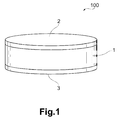
- FIG. 1 is a schematic view showing one preferable embodiment of the dielectric element of the present invention.
- the dielectric element 100 as shown in Figure 1 forms a capacitor having a disc-like dielectric body 1 and a pair of electrodes 2 and 3 disposed on both surfaces of the dielectric body 1.
- the dielectric body 1 is formed by a dielectric ceramic composition represented by the following formula (1). ⁇ [(Bi s Na t ) a (Bi u K v ) b Ba c ] 1-d A d ⁇ x Ti 1-d Nb d O 3 (1)
- A represents at least one element selected from the group consisting of Li, Na and K
- such a dielectric ceramic composition is capable of providing a relative permittivity of 1000 or more and also decreasing the variation rate of DC bias to a very low level of -15% or less under an electric field of 5 V/ ⁇ m.
- the dielectric ceramic of the present invention is a combination of ferroelectric composition and antiferroelectric composition. With such a specific combination, a dielectric ceramic composition with a relatively high relative permittivity and good DC bias related properties can be provided.
- the a, b and c are not preferred to go beyond the ranges mentioned above. If they go beyond the ranges, the relative permittivity will become 1000 or less, the variation rate of DC bias under an electric field of 5 V/ ⁇ m will become -15% or more and the withstand voltage will decrease.
- the d is neither preferred to be less than 0.10 nor more than 0.50. If d is less than 0.10, the DC bias related properties may deteriorate. If d is more than 0.50, the permittivity will be less than 1000.
- the s+u, t and v are not preferred to go beyond the ranges mentioned above. Otherwise, defects will be generated and no sufficient sintering density will be provided. In addition, charges will be leaked and the withstand voltage decreases.
- the amount of the complex oxides represented by formula (1) preferably accounts for 90 mass% or more based on the whole dielectric ceramic composition.
- impurities such as P and Zr which may be mixed during the preparation processes can also be contained.
- the composition of the dielectric ceramic composition can be measured by, for example, the X-ray fluorescence analysis or the ICP emission spectrometric analysis.
- the dielectric ceramic composition preferably has a relative density of 95% or more.
- the relative density refers to the actually measured value of density relative to the theoretical density.
- the theoretical density is calculated based on the lattice constant obtained via X-ray diffraction and the stoichiometric ratio obtained when the composition is assumed to be a perfect crystal.
- the relative density of the dielectric ceramic composition can be measured by, for example, the Archimedes method.
- the relative density of the dielectric ceramic composition can be adjusted by changing the temperature or the time in the firing process.
- the powders of bismuth oxide (Bi 2 O 3 ), sodium carbonate (Na 2 CO 3 ), potassium carbonate (K 2 CO 3 ), barium carbonate (BaCO 3 ), titanium oxide (TiO 2 ), niobium oxide (Nb 2 O 5 ) and the like are prepared as the staring materials for the dielectric body 1.
- the mixture obtained from the wetting mixing is subjected to a calcinating process to provide a calcined mixture.
- the calcinating process is usually performed in air.
- the temperature during the calcinating process is preferred to be 700 to 900°C, and the time is preferred to be 1 to 10 hours.
- the pulverized powder is dried to provide a powder of the calcined mixture.
- a binder in a small amount is added to the obtained powder of calcined mixture, and a press molding process is performed to provide a molded body.
- the pressure during the molding process is preferably about 5 t/cm 2 .
- the shape of the molded body is not particularly restricted.
- the molded body can be made into a disc-like one with a planar size of ⁇ 17mm and a thickness of about 1 mm.
- the obtained molded body is fired to prepare a sample of the dielectric ceramic composition.
- the firing process is usually performed in air.
- the temperature during the firing process is preferred to be 950 to 1300°C, and the time is preferred to be 2 to 10 hours.
- Metallic electrodes of silver or the like are formed on both surfaces of the resultant sample of the dielectric ceramic composition.
- the formation of the electrodes is performed by a method such as vapor deposition, sputtering, enameling, electroless plating or the like.
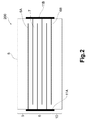
- Figure 2 is a cross-sectional view showing another embodiment of the dielectric element of the present invention.
- the laminated dielectric element 200 shown in Figure 2 has a rectangular laminated body 5 and a pair of terminal electrodes 11A and 11B respectively formed on the opposite end planes of the laminated body 5.
- the laminated body 5 consists of a green body 8 and a pair of protection layers 9 and 10, wherein the green body 8 is formed by alternatively laminating internal electrode layers (electrode layers) 6A and 6B with a dielectric layer 7 interposed between 6A and 6B, and the pair of protection layers 9 and 10 are disposed to sandwich the green body 8 from the two end plane sides in the laminating direction (from top to bottom in the figure).
- the dielectric layer 7 and the internal electrodes 6A and 6B are alternatively laminated.
- the dielectric layer 7 is a layer composed of the dielectric ceramic composition of the present invention.
- the thickness of each layer of the dielectric layer 7 can be randomly set.
- the thickness can be 1 to 100 ⁇ m.
- the internal electrode layers 6A and 6B are disposed to be parallel to each other.
- the internal electrode layer 6A is formed in such a manner that one end is exposed to the end plane in the laminated body 5 where the terminal electrode 11A is formed.
- the internal electrode layer 6B is formed in such a manner that one end is exposed to the end plane in the laminated body 5 where the terminal electrode 11B is formed.
- the internal electrode layer 6A and the internal electrode layer 6B are disposed in such a manner that most of the two electrode layers overlap in the laminating direction.
- metals such as Au, Pt or Ag can be used as the material for the internal electrode layers 6A and 6B.
- terminal electrodes 11A and 11B are respectively in contact with the end portion of the internal electrode layer 6A or 6B exposed to the mentioned end planes.
- the terminal electrodes 11A and 11B are respectively electrically connected to the internal electrode layers 6A and 6B.
- the terminal electrodes 11A and 11B can be formed by conductive material having Ag, Au, Cu and the like as the main component(s).
- the thickness of the terminal electrodes 11A and 11B can be properly set depending on the uses or the size of the laminated dielectric element. For example, the thickness can be 10 to 50 ⁇ m.
- dielectric ceramic composition and the dielectric element of the present embodiments have been described above. These dielectric ceramic compositions have good DC bias related properties when a high electric field is applied and thus can be suitably utilized in a mid-high voltage capacitor with a relatively high rated voltage.
- the present invention is not limited to the embodiments mentioned above.
- the constituents other than the dielectric ceramic composition well known ones can be used.
- the powder of calcined mixture can be prepared through hydrothermal synthesis method.
- (BiNa)TiO 3 , (BiK)TiO 3 , BaTiO 3 and NaNbO 3 can be prepared, mixed and sintered to function as the precursor.
- the powders of bismuth oxide (Bi 2 O 3 ), sodium carbonate (Na 2 CO 3 ), potassium carbonate (K 2 CO 3 ), barium carbonate (BaCO 3 ), titanium oxide (TiO 2 ) and niobium oxide (Nb 2 O 5 ) were prepared as the staring materials.
- powder of lithium carbonate (Li 2 CO 3 ) was further prepared.
- the powder of potassium carbonate (K 2 CO 3 ) was additionally prepared besides the starting materials mentioned above.
- a, b, c, d, s+u, t, v and x in Table 1 respectively represents the numerical value of a, b, c, d, s+u, t, v and x in the following formula (1).
- component A was Na.
- component A was Li.
- component A was K in Example 16 and was Na and K in Example 17.
- each weighed starting powder material was wet mixed by a ball mill, and the resultant mixture was subjected to a calcinating process in air at a temperature of 850°C for 2 hours to provide a calcined mixture.
- the obtained calcined mixture was wet pulverized by a ball mill to provide the powder of the calcined mixture.
- the powder of calcined mixture was added with a binder in a small amount and was molded under a pressure of about 5 t/cm 2 to provide a disc-like molded body having a planar size of ⁇ 17mm and a thickness of 1 mm.
- the obtained molded body was fired in air for 2 to 10 hours at a firing temperature of 950 to 1300°C to provide a relative density of 95%.
- a sample of the dielectric ceramic composition was obtained.
- a density measurement was provided to the obtained dielectric ceramic sample, and the density was 95% or more relative to the theoretical density in all samples.
- composition was analyzed in the obtained dielectric ceramic composition sample. The results were equivalent to the composition ratios in the weighed components.
- the Ag electrodes were provided to both surfaces of the obtained dielectric ceramic composition sample through vapor deposition to prepare a dielectric element.
- the relative permittivity at room temperature of 25°C and the DC bias related properties were shown in Table 1.
- the short straight line in the Table meant no specific value had been obtained due to the charge leakage during the measurement.
- the sample without breakdown was labeled with 'o' and the one with breakdown was labeled with ' ⁇ '.
- the sample was deemed as a good one when the relative permittivity was 1000 or higher, the variation rate of DC bias was -15% or less under an electric field of 5V/ ⁇ m and without breakdown under a direct current electric field of 10 V/ ⁇ m.
Landscapes
- Engineering & Computer Science (AREA)
- Chemical & Material Sciences (AREA)
- Ceramic Engineering (AREA)
- Power Engineering (AREA)
- Manufacturing & Machinery (AREA)
- Materials Engineering (AREA)
- Inorganic Chemistry (AREA)
- Microelectronics & Electronic Packaging (AREA)
- Structural Engineering (AREA)
- Organic Chemistry (AREA)
- Compositions Of Oxide Ceramics (AREA)
- Inorganic Insulating Materials (AREA)
- Ceramic Capacitors (AREA)
- Fixed Capacitors And Capacitor Manufacturing Machines (AREA)
Abstract
Description
- The present invention relates to a dielectric ceramic composition and an electronic component using the same. In particular, the present invention relates to a dielectric ceramic composition and a dielectric element that can be suitably utilized in a mid-high voltage application with a relatively high rated voltage.
- In recent years, as the electronic circuits are disposed in a high density, the requirement for the miniaturization of electronic component is increasing. Besides, as the laminated ceramic capacitor is quickly developed to have a small size and a large capacity, more applications are provided and various properties are required.
- For example, in a capacitor having a rated voltage higher than 100 V for mid-high voltage application, a high electrostatic capacity is required under an electric field with a high intensity, wherein the mentioned capacitor for mid-high voltage application is used in an ECM (engine electric computer module), a fuel injecting device, an electronic controlled throttle, an inverter, a converter, an HID head lamp unit, a battery controlling unit for a hybrid engine, a digital still camera or the like.
- However, the conventional dielectric ceramic composition is designed on the premise of being used under a direct voltage having a low electric field intensity of, for example, about 1 V/µm, so the used laminated ceramic capacitor is developed to be thinner and thinner. If such a ceramic capacitor is used under an electric field with a high intensity, a problem rises that the variation rate of the electrostatic capacity relative to the applied direct current electric field (hereinafter referred to as the variation rate of DC bias) becomes larger.
- If the variation rate of DC bias is large, the effective capacity in the laminated ceramic capacitor will decrease, and the required electrostatic capacity in the designing stage will not be satisfied. Thus, there might be problems such as the behavior of the electronic device using the laminated ceramic capacitor becomes unstable or even the electronic device does not work anymore.
- Therefore, with respect to a capacitor to be used in a high electric field, the variation rate of DC bias should be small. Besides, a dielectric ceramic composition is expected to be used which has a high permittivity when a high electric field is applied. In addition, the "high electric constant" described here refers to, for instance, an intensity of 5 V/µm for the electric field, and a high permittivity refers to, for example, 1000.
- In order to solve the technical problem mentioned above, the following
Patent Document 1 has disclosed a dielectric ceramic composition with the following characteristics. In particular, it contains a main component and a subcomponent, wherein the main component consists of barium titanate having 0.02 wt% or less of oxide of alkali metal(s), at least one selected from the group consisting of europium oxide, gadolinium oxide, terbium oxide, dysprosium oxide, holmium oxide, erbium oxide, thulium oxide and ytterbium oxide, barium zirconate, magnesium oxide, manganese oxide and can be represented by the formula of (BaO)mTiO2+αR2O3+βBaZrO3+γMgO+gMnO (in the formula, R2O3 is at least one selected from the group consisting of Eu2O3, Gd2O3, Tb2O3, Dy2O3, Ho2O3, Er2O3, Tm2O3 and Yb2O3, α, β, γ and g represent the molar ratios, and 0.001≤α≤0.06, 0.005≤β≤0.06, 0.001<γ≤0.12, 0.001<g≤0.12, γ+g≤0.13, and 1.000<m≤1.035), and the subcomponent is silicone oxide contained in an amount of 0.2 to 5.0 mol calculated in terms of SiO2 relative to 100 mol of the main component. - However, even though the ceramic capacitor using the dielectric ceramic composition shown in
Patent Document 1 as the dielectric material has a relatively high relative permittivity of about 1500, it has a high variation rate of DC bias as large as -45% or less under an electric field of 5 V/µm. In this respect, the DC bias related properties are expected to be further improved. - In addition,
Patent Document 2 has disclosed a dielectric ceramic composition as follows. In particular, it is a dielectric ceramic which contains Ca, Sr, Mg, Mn and rare earth element(s), and the dielectric ceramic contains main grains which are formed by dissolving at least part of the Ca, Sr, Mg, Mn and the rare earth element(s) as solid solute in perovskite-type grains of barium titanate (BCT-type grains) in which part of A site is replaced by the Ca. In the dielectric ceramic, the amount of Al is 0.01 mass% or less when calculated in terms of oxides. The main grains have a higher concentration of Ca at the grain surface than that at the grain center and are of a core-shell structure with Sr, Mg, Mn and the rare earth element(s) unevenly distributed at the grain surface. Further, the grains have an average grain size of 0.1 to 0.5 µm. - However, although the BCT-type dielectric ceramic composition as shown in
Patent Document 2 has a large relative permittivity of 2500 or more, it has a large variation rate of DC bias of -70% or less under an electric field of 5 V/µm. Thus, the DC bias related properties cannot be said to be good. -
- Patent Document 1:
JP-A-H11-322414 - Patent Document 2:
JP-A-2006-206362 - The present invention is made in view of the actual situations and aims to provide a dielectric ceramic composition and that can be suitably utilized in a mid-high voltage application with a relatively high rated voltage and has a very small variation rate of DC bias of -15% or less under an electric field of 5 V/µm and also a relatively high relative permittivity of 1000 or more. The present invention also aims to provide a dielectric element using this dielectric ceramic composition.
- In order to reach the goal mentioned above, the present invention provides a dielectric ceramic composition composed of the complex oxides represented by the following formula (1).
{[(BisNat)a(BiuKv)bBac]1-dAd}xTi1-dNbdO3 (1)
- In formula (1), A represents at least one element selected from the group consisting of Li, Na and K, and a, b, c, d, s, t, u, v and x are numbers respectively satisfying the following formulae.






- With the constitution mentioned above, the dielectric ceramic composition of the present invention has a very small variation rate of DC bias of -15% or less under an electric field of 5 V/µm, and a relatively high relative permittivity of 1000 or more can be provided.
- In addition, the present invention provides a dielectric element containing the dielectric ceramic composition mentioned above.
- Such a dielectric element contains the dielectric ceramic composition mentioned above, so it is useful to a capacitor to which a large permittivity is necessary when a high electric field is applied such as a capacitor used in an electric circuit to protect the electric circuit when a high electric field is applied.
- According to the present invention, a dielectric ceramic composition will be provided that can be suitably utilized in a mid-high voltage application with a relatively high rated voltage and has a very small variation rate of DC bias of -15% or less under an electric field of 5 V/µm and also a relatively high relative permittivity of 1000 or more. Also, a dielectric element using this dielectric ceramic composition will be provided.
-
-
Figure 1 is a schematic view showing one preferable embodiment of the dielectric element of the present invention. -
Figure 2 is a cross-sectional view showing another embodiment of the dielectric element of the present invention. - Hereinafter, the preferable embodiments of the present invention will be described depending on cases with reference to the drawings. In each figure, the same symbol is marked for the same or equivalent element and repeated descriptions will be omitted.
-
Figure 1 is a schematic view showing one preferable embodiment of the dielectric element of the present invention. Thedielectric element 100 as shown inFigure 1 forms a capacitor having a disc-likedielectric body 1 and a pair ofelectrodes dielectric body 1. - The
dielectric body 1 is formed by a dielectric ceramic composition represented by the following formula (1).
{[(BisNat)a(BiuKv)bBac]1-dAd}xTi1-dNbdO3 (1)
- In formula (1), A represents at least one element selected from the group consisting of Li, Na and K, and a, b, c, d, s, t, u, v and x are numbers respectively satisfy the following formulae.


- With the constitution mentioned above, such a dielectric ceramic composition is capable of providing a relative permittivity of 1000 or more and also decreasing the variation rate of DC bias to a very low level of -15% or less under an electric field of 5 V/µm.
- The dielectric ceramic of the present invention is a combination of ferroelectric composition and antiferroelectric composition. With such a specific combination, a dielectric ceramic composition with a relatively high relative permittivity and good DC bias related properties can be provided.
- The a, b and c are not preferred to go beyond the ranges mentioned above. If they go beyond the ranges, the relative permittivity will become 1000 or less, the variation rate of DC bias under an electric field of 5 V/µm will become -15% or more and the withstand voltage will decrease.
- The d is neither preferred to be less than 0.10 nor more than 0.50. If d is less than 0.10, the DC bias related properties may deteriorate. If d is more than 0.50, the permittivity will be less than 1000.
- The s+u, t and v are not preferred to go beyond the ranges mentioned above. Otherwise, defects will be generated and no sufficient sintering density will be provided. In addition, charges will be leaked and the withstand voltage decreases.
- No sufficient sintering density will be provided and the insulation resistance will decrease if x is less than 0.95 or more than 1.05. As a result, the dielectric ceramic composition is difficult to be used when a high electrical field is applied.
- From the viewpoint of a sufficient permittivity for the application as a dielectric ceramic composition, the amount of the complex oxides represented by formula (1) preferably accounts for 90 mass% or more based on the whole dielectric ceramic composition. For the remaining part, in addition to the subcomponents such as paraelectric ceramic composition, impurities such as P and Zr which may be mixed during the preparation processes can also be contained.
- Here, the composition of the dielectric ceramic composition can be measured by, for example, the X-ray fluorescence analysis or the ICP emission spectrometric analysis.
- The dielectric ceramic composition preferably has a relative density of 95% or more. Here, in the specification of the present invention, the relative density refers to the actually measured value of density relative to the theoretical density. The theoretical density is calculated based on the lattice constant obtained via X-ray diffraction and the stoichiometric ratio obtained when the composition is assumed to be a perfect crystal. The relative density of the dielectric ceramic composition can be measured by, for example, the Archimedes method. Here, the relative density of the dielectric ceramic composition can be adjusted by changing the temperature or the time in the firing process.
- Next, one example of the method for preparing the dielectric element shown in
Figure 1 will be described. - First of all, the powders of bismuth oxide (Bi2O3), sodium carbonate (Na2CO3), potassium carbonate (K2CO3), barium carbonate (BaCO3), titanium oxide (TiO2), niobium oxide (Nb2O5) and the like are prepared as the staring materials for the
dielectric body 1. - These mentioned starting powders are weighed to make the dielectric ceramic composition (sintered body) after the official firing process will satisfy the composition of the dielectric ceramic composition of the present embodiment.
- Then, all the weighed starting powder is wet mixed by a ball mill or the like. Thereby, the mixture obtained from the wetting mixing is subjected to a calcinating process to provide a calcined mixture. Here, the calcinating process is usually performed in air. In addition, the temperature during the calcinating process is preferred to be 700 to 900°C, and the time is preferred to be 1 to 10 hours.
- After the calcined mixture is wet pulverized by a ball mill or the like, the pulverized powder is dried to provide a powder of the calcined mixture. Thereafter, a binder in a small amount is added to the obtained powder of calcined mixture, and a press molding process is performed to provide a molded body. Here, the pressure during the molding process is preferably about 5 t/cm2. The shape of the molded body is not particularly restricted. For example, the molded body can be made into a disc-like one with a planar size of φ17mm and a thickness of about 1 mm.
- Then, the obtained molded body is fired to prepare a sample of the dielectric ceramic composition. Here, the firing process is usually performed in air. In addition, the temperature during the firing process is preferred to be 950 to 1300°C, and the time is preferred to be 2 to 10 hours.
- Metallic electrodes of silver or the like are formed on both surfaces of the resultant sample of the dielectric ceramic composition. The formation of the electrodes is performed by a method such as vapor deposition, sputtering, enameling, electroless plating or the like.
-
Figure 2 is a cross-sectional view showing another embodiment of the dielectric element of the present invention. The laminateddielectric element 200 shown inFigure 2 has a rectangularlaminated body 5 and a pair ofterminal electrodes laminated body 5. - The
laminated body 5 consists of agreen body 8 and a pair ofprotection layers green body 8 is formed by alternatively laminating internal electrode layers (electrode layers) 6A and 6B with adielectric layer 7 interposed between 6A and 6B, and the pair ofprotection layers green body 8 from the two end plane sides in the laminating direction (from top to bottom in the figure). In thegreen body 8, thedielectric layer 7 and theinternal electrodes - The
dielectric layer 7 is a layer composed of the dielectric ceramic composition of the present invention. - The thickness of each layer of the
dielectric layer 7 can be randomly set. For example, the thickness can be 1 to 100 µm. - The
internal electrode layers internal electrode layer 6A is formed in such a manner that one end is exposed to the end plane in thelaminated body 5 where theterminal electrode 11A is formed. In addition, theinternal electrode layer 6B is formed in such a manner that one end is exposed to the end plane in thelaminated body 5 where theterminal electrode 11B is formed. Further, theinternal electrode layer 6A and theinternal electrode layer 6B are disposed in such a manner that most of the two electrode layers overlap in the laminating direction. - As the material for the
internal electrode layers - On the end planes of the
laminated body 5 where theterminal electrodes internal electrode layer terminal electrodes internal electrode layers terminal electrodes terminal electrodes - The dielectric ceramic composition and the dielectric element of the present embodiments have been described above. These dielectric ceramic compositions have good DC bias related properties when a high electric field is applied and thus can be suitably utilized in a mid-high voltage capacitor with a relatively high rated voltage.
- The present invention is not limited to the embodiments mentioned above. For example, as the constituents other than the dielectric ceramic composition, well known ones can be used. Further, for example, in the preparation of the dielectric element mentioned above, the powder of calcined mixture can be prepared through hydrothermal synthesis method. In addition, (BiNa)TiO3, (BiK)TiO3, BaTiO3 and NaNbO3 can be prepared, mixed and sintered to function as the precursor.
- Hereinafter, the present invention will be further described in detail based on Examples and Comparative Examples. However, the present invention is not limited to the following Examples.
- In order to prepare a dielectric ceramic composition, the powders of bismuth oxide (Bi2O3), sodium carbonate (Na2CO3), potassium carbonate (K2CO3), barium carbonate (BaCO3), titanium oxide (TiO2) and niobium oxide (Nb2O5) were prepared as the staring materials. In Example 15, in addition to the starting materials mentioned above, powder of lithium carbonate (Li2CO3) was further prepared. For Examples 16 and 17, the powder of potassium carbonate (K2CO3) was additionally prepared besides the starting materials mentioned above.
- These mentioned starting powder materials were weighed to make the dielectric ceramic composition (sintered body) after the official firing process satisfy the composition shown in Table 1. In addition, here, a, b, c, d, s+u, t, v and x in Table 1 respectively represents the numerical value of a, b, c, d, s+u, t, v and x in the following formula (1). In the Comparative Examples and Examples other than Examples 15 to 17, component A was Na. In Example 15, component A was Li. Further, component A was K in Example 16 and was Na and K in Example 17.
{[(BisNat)a(BiuKv)bBac]1-dAd}xTi1-dNbdO3 (1)
- Then, each weighed starting powder material was wet mixed by a ball mill, and the resultant mixture was subjected to a calcinating process in air at a temperature of 850°C for 2 hours to provide a calcined mixture. The obtained calcined mixture was wet pulverized by a ball mill to provide the powder of the calcined mixture. Thereafter, the powder of calcined mixture was added with a binder in a small amount and was molded under a pressure of about 5 t/cm2 to provide a disc-like molded body having a planar size of φ17mm and a thickness of 1 mm.
- Then, the obtained molded body was fired in air for 2 to 10 hours at a firing temperature of 950 to 1300°C to provide a relative density of 95%. In this way, a sample of the dielectric ceramic composition was obtained. A density measurement was provided to the obtained dielectric ceramic sample, and the density was 95% or more relative to the theoretical density in all samples.
- The composition was analyzed in the obtained dielectric ceramic composition sample. The results were equivalent to the composition ratios in the weighed components.
- The Ag electrodes were provided to both surfaces of the obtained dielectric ceramic composition sample through vapor deposition to prepare a dielectric element.
- The DC bias related properties were tested with the maximal intensity of the applied electric filed Emax being 5V/µm for each obtained dielectric element.
- A withstanding voltage test was performed on each dielectric element under a direct current electric field of 10 V/µm.
- The relative permittivity at room temperature of 25°C and the DC bias related properties were shown in Table 1. In addition, the short straight line in the Table meant no specific value had been obtained due to the charge leakage during the measurement. Further, as for items of the withstanding voltage test in the table, the sample without breakdown was labeled with 'o' and the one with breakdown was labeled with '×'. The sample was deemed as a good one when the relative permittivity was 1000 or higher, the variation rate of DC bias was -15% or less under an electric field of 5V/µm and without breakdown under a direct current electric field of 10 V/µm.
[Table 1] a b c d x s+u t v A Permittivity (0V/µm) Permittivity (5V/µm) Variation rate of DC bias (5V/µm) Withstanding voltage test (10V/µm) Comparative Example 1 0.85 0.09 0.05 0.09 0.99 1.00 0.50 0.50 Na 1707 1426 -16.5 ○ Comparative Example 2 0.00 0.50 0.50 0.10 0.99 1.00 0.50 0.50 Na 1708 1284 -24.8 ○ Comparative Example 3 0.05 0.90 0.05 0.10 0.99 1.00 0.50 0.50 Na 903 832 -7.9 ○ Comparative Example 4 0.10 0.10 0.80 0.10 0.99 1.00 0.50 0.50 Na 2323 1929 -16.9 ○ Example 1 0.10 0.80 0.10 0.10 0.99 1.00 0.50 0.50 Na 1191 1179 -1.0 ○ Example 2 0.10 0.85 0.05 0.10 0.99 1.00 0.50 0.50 Na 1222 1198 -2.0 ○ Example 3 0.25 0.05 0.70 0.10 0.99 1.00 0.50 0.50 Na 1204 1132 -6.0 ○ Example 4 0.33 0.33 0.33 0.10 0.99 1.00 0.50 0.50 Na 1962 1911 -2.6 ○ Comparative Example 5 0.50 0.00 0.50 0.10 0.99 1.00 0.50 0.50 Na 2473 2318 -6.2 × Example 5 0.60 0.20 0.20 0.10 0.99 1.00 0.50 0.50 Na 2078 1872 -9.9 ○ Example 6 0.80 0.10 0.10 0.10 0.99 1.00 0.50 0.50 Na 2071 1860 -10.2 ○ Example 7 0.85 0.09 0.05 0.10 0.99 1.00 0.50 0.50 Na 2056 1759 -14.4 ○ Example 8 0.90 0.01 0.09 0.10 0.99 1.00 0.50 0.50 Na 2008 1882 -6.3 ○ Comparative Example 6 0.95 0.00 0.05 0.10 0.99 1.00 0.50 0.50 Na 1910 1839 -3.7 × Example 9 0.33 0.33 0.33 0.20 0.99 1.00 0.50 0.50 Na 2278 2188 -4.0 ○ Comparative Example 7 0.33 0.33 0.33 0.30 0.93 1.00 0.50 0.50 Na - - - × Example 10 0.33 0.33 0.33 0.30 0.95 1.00 0.50 0.50 Na 2077 1957 -5.8 ○ Comparative Example 8 0.33 0.33 0.33 0.30 0.99 0.80 0.45 0.45 Na 2019 1898 -6.0 × Example 11 0.33 0.33 0.33 0.30 0.99 0.90 0.45 0.45 Na 2001 1913 -4.4 ○ Comparative Example 9 0.33 0.33 0.33 0.30 0.99 0.95 0.40 0.50 Na - - - × Example 12 0.33 0.33 0.33 0.30 0.99 0.95 0.45 0.50 Na 1990 1910 -4.0 ○ Comparative 0.33 0.33 0.33 0.30 0.99 0.95 0.50 0.40 Na - - - × Example 10 Example 13 0.33 0.33 0.33 0.30 0.99 0.95 0.50 0.45 Na 1972 1927 -2.3 ○ Example 14 0.33 0.33 0.33 0.30 0.99 1.00 0.50 0.50 Na 2056 1922 -6.5 ○ Example 15 0.33 0.33 0.33 0.30 0.99 1.00 0.50 0.50 Li 2052 1917 -6.6 ○ Example 16 0.33 0.33 0.33 0.30 0.99 1.00 0.50 0.50 K 2063 1926 -6.6 ○ Example 17 0.33 0.33 0.33 0.30 0.99 1.00 0.50 0.50 Na, K 2019 1897 -6.0 ○ Comparative Example 11 0.33 0.33 0.33 0.30 0.99 1.00 0.50 0.55 Na 2101 - - × Comparative Example 12 0.33 0.33 0.33 0.30 0.99 1.00 0.55 0.50 Na 2043 - - × Comparative Example 13 0.33 0.33 0.33 0.30 0.99 1.10 0.50 0.50 Na 2012 1895 -5.8 × Example 18 0.33 0.33 0.33 0.30 1.05 1.00 0.50 0.50 Na 2028 1875 -7.5 ○ Comparative Example 14 0.33 0.33 0.33 0.30 1.06 1.00 0.50 0.50 Na 2043 1908 -6.6 × Example 19 0.60 0.20 0.20 0.30 0.99 1.00 0.50 0.50 Na 2449 2218 -9.4 ○ Example 20 0.80 0.10 0.10 0.30 0.99 1.00 0.50 0.50 Na 1958 1838 -6.1 ○ Example 21 0.85 0.09 0.05 0.30 0.99 1.00 0.50 0.50 Na 1730 1633 -5.6 ○ Example 22 0.33 0.33 0.33 0.40 0.99 1.00 0.50 0.50 Na 1914 1732 -9.5 ○ Comparative Example 15 0.10 0.15 0.75 0.50 0.99 1.00 0.50 0.50 Na 2406 1963 -18.4 ○ Example 23 0.10 0.85 0.05 0.50 0.99 1.00 0.50 0.50 Na 1080 1074 -0.6 ○ Example 24 0.25 0.05 0.70 0.50 0.99 1.00 0.50 0.50 Na 1062 1006 -5.3 ○ Example 25 0.85 0.09 0.05 0.50 0.99 1.00 0.50 0.50 Na 1402 1366 -2.6 ○ Example 26 0.90 0.01 0.09 0.50 0.99 1.00 0.50 0.50 Na 1501 1477 -1.6 ○ Comparative Example 16 0.33 0.33 0.33 0.60 0.99 1.00 0.50 0.50 Na 997 982 -1.5 × - It can be confirmed from Table 1 that the dielectric ceramic compositions of Examples 1 to 26 had a small variation rate of DC bias and a sufficiently large permittivity for application when a high electric field was applied.
-
- 1
- dielectric body
- 2,3
- electrode
- 5
- laminated body
- 6A,6B
- internal electrode layer
- 7
- dielectric layer
- 8
- green body
- 9,10
- protection layer
- 11A,11B
- terminal electrode
- 100
- dielectric element
- 200
- laminated dielectric element
Claims (2)
- A dielectric ceramic composition comprising a composition represented by the following formula (1),
{[(BisNat)a(BiuKv)bBac]1-dAd}xTi1-dNbdO3 (1),
wherein, in formula (1), A represents at least one element selected from the group consisting of Li, Na and K, and
a, b, c, d, s, t, u, v and x are numbers respectively satisfying the following formulae,


- A dielectric element comprising the dielectric ceramic composition of claim 1.
Applications Claiming Priority (2)
| Application Number | Priority Date | Filing Date | Title |
|---|---|---|---|
| JP2013067857A JP6102410B2 (en) | 2013-03-28 | 2013-03-28 | Dielectric porcelain composition and dielectric element |
| PCT/JP2014/052480 WO2014156302A1 (en) | 2013-03-28 | 2014-02-04 | Dielectric ceramic composition and dielectric element |
Publications (3)
| Publication Number | Publication Date |
|---|---|
| EP2980043A1 true EP2980043A1 (en) | 2016-02-03 |
| EP2980043A4 EP2980043A4 (en) | 2016-12-28 |
| EP2980043B1 EP2980043B1 (en) | 2018-01-17 |
Family
ID=51623303
Family Applications (1)
| Application Number | Title | Priority Date | Filing Date |
|---|---|---|---|
| EP14775500.3A Active EP2980043B1 (en) | 2013-03-28 | 2014-02-04 | Dielectric ceramic composition and dielectric element |
Country Status (5)
| Country | Link |
|---|---|
| US (1) | US9530563B2 (en) |
| EP (1) | EP2980043B1 (en) |
| JP (1) | JP6102410B2 (en) |
| CN (1) | CN105073684B (en) |
| WO (1) | WO2014156302A1 (en) |
Families Citing this family (18)
| Publication number | Priority date | Publication date | Assignee | Title |
|---|---|---|---|---|
| JP6102405B2 (en) * | 2013-03-27 | 2017-03-29 | Tdk株式会社 | Dielectric porcelain composition and dielectric element |
| JP2016060647A (en) * | 2014-09-12 | 2016-04-25 | エプコス アクチエンゲゼルシャフトEpcos Ag | Dielectric composition, dielectric element, electronic component and laminated electronic component |
| KR102115523B1 (en) * | 2014-12-08 | 2020-05-26 | 삼성전기주식회사 | Dielectric ceramic composition and multilayer ceramic capacitor comprising the same |
| KR102098459B1 (en) * | 2015-05-27 | 2020-04-07 | 티디케이 일렉트로닉스 아게 | Bismuth sodium strontium titanate-based dielectric composition, dielectric element, electronic component and multilayer electronic component thereof |
| KR20180008769A (en) * | 2015-05-27 | 2018-01-24 | 에프코스 아게 | Bismuth sodium strontium titanate based dielectric composition, dielectric element, electronic part and laminated electronic part thereof |
| EP3326178B1 (en) * | 2015-07-17 | 2019-05-22 | TDK Electronics AG | Dielectric composition, dielectric element, electronic component and laminated electronic component |
| JP6655707B2 (en) * | 2015-07-17 | 2020-02-26 | ティーディーケイ・エレクトロニクス・アクチェンゲゼルシャフトTdk Electronics Ag | Dielectric composition, dielectric element, electronic component and laminated electronic component |
| EP3326182B1 (en) * | 2015-07-17 | 2022-03-23 | TDK Electronics AG | Dielectric composition, dielectric element, electronic component and laminated electronic component |
| WO2017012797A1 (en) * | 2015-07-17 | 2017-01-26 | Epcos Ag | Dielectric composition, dielectric element, electronic component and multi-layer electronic component |
| WO2017012800A1 (en) * | 2015-07-17 | 2017-01-26 | Epcos Ag | Dielectric composition, dielectric element, electronic component and laminated electronic component |
| JP6591656B2 (en) * | 2015-07-17 | 2019-10-16 | ティーディーケイ・エレクトロニクス・アクチェンゲゼルシャフトTdk Electronics Ag | Dielectric composition, dielectric element, electronic component and laminated electronic component |
| CN107851516B (en) | 2015-07-17 | 2020-03-06 | 埃普科斯股份有限公司 | Dielectric composition, dielectric element, electronic component, and laminated electronic component |
| JP6588620B2 (en) | 2015-07-17 | 2019-10-09 | ティーディーケイ・エレクトロニクス・アクチェンゲゼルシャフトTdk Electronics Ag | Multilayer ceramic capacitor |
| JP6457415B2 (en) * | 2016-03-10 | 2019-01-23 | 太陽誘電株式会社 | Piezoelectric element and manufacturing method thereof |
| KR101853191B1 (en) | 2016-07-28 | 2018-04-27 | 삼성전기주식회사 | Dielectric ceramic composition, multilayer ceramic capacitor including the dielectric ceramic composition, and method for fabricating the multilayer ceramic capacitor |
| KR102847109B1 (en) * | 2021-01-29 | 2025-08-14 | 삼성전자주식회사 | Dielectric material, preparing method thereof, and device comprising dielectric material |
| KR20230055288A (en) * | 2021-10-18 | 2023-04-25 | 삼성전자주식회사 | Capacitor device and semiconductor device including the same |
| KR20240093098A (en) | 2022-12-15 | 2024-06-24 | 삼성전기주식회사 | Multilayer electronic component |
Family Cites Families (8)
| Publication number | Priority date | Publication date | Assignee | Title |
|---|---|---|---|---|
| JP3334607B2 (en) | 1998-05-12 | 2002-10-15 | 株式会社村田製作所 | Dielectric ceramic composition and multilayer ceramic capacitor |
| JP4674405B2 (en) * | 2000-11-21 | 2011-04-20 | Tdk株式会社 | Piezoelectric ceramic |
| CN1197823C (en) * | 2000-11-21 | 2005-04-20 | Tdk株式会社 | Piezoelectric Ceramics |
| JP4067298B2 (en) * | 2001-02-22 | 2008-03-26 | Tdk株式会社 | Piezoelectric ceramic |
| JP2006206362A (en) | 2005-01-27 | 2006-08-10 | Kyocera Corp | Dielectric porcelain and multilayer ceramic capacitor using the same |
| JP5435732B2 (en) * | 2010-04-28 | 2014-03-05 | Necトーキン株式会社 | Piezoelectric ceramic composition |
| JP6016333B2 (en) * | 2011-05-27 | 2016-10-26 | キヤノン株式会社 | Sodium niobate powder, method for producing sodium niobate powder, plate-like particles, method for producing plate-like particles, method for producing oriented ceramics |
| JP6102405B2 (en) * | 2013-03-27 | 2017-03-29 | Tdk株式会社 | Dielectric porcelain composition and dielectric element |
-
2013
- 2013-03-28 JP JP2013067857A patent/JP6102410B2/en active Active
-
2014
- 2014-02-04 CN CN201480017478.3A patent/CN105073684B/en active Active
- 2014-02-04 EP EP14775500.3A patent/EP2980043B1/en active Active
- 2014-02-04 US US14/780,017 patent/US9530563B2/en active Active
- 2014-02-04 WO PCT/JP2014/052480 patent/WO2014156302A1/en not_active Ceased
Also Published As
| Publication number | Publication date |
|---|---|
| EP2980043B1 (en) | 2018-01-17 |
| JP2014189465A (en) | 2014-10-06 |
| EP2980043A4 (en) | 2016-12-28 |
| CN105073684A (en) | 2015-11-18 |
| JP6102410B2 (en) | 2017-03-29 |
| US20160049248A1 (en) | 2016-02-18 |
| CN105073684B (en) | 2018-03-02 |
| US9530563B2 (en) | 2016-12-27 |
| WO2014156302A1 (en) | 2014-10-02 |
Similar Documents
| Publication | Publication Date | Title |
|---|---|---|
| EP2980043B1 (en) | Dielectric ceramic composition and dielectric element | |
| CN114334447B (en) | Laminated ceramic capacitor | |
| JP5151990B2 (en) | Dielectric ceramic and multilayer ceramic capacitor using the same | |
| KR102351180B1 (en) | Multi-layered ceramic capacitor | |
| US8526165B2 (en) | Dielectric ceramic and laminated ceramic capacitor | |
| EP3191427B1 (en) | Dielectric composition, dielectric element, electronic component and laminated electronic component | |
| US11066332B2 (en) | Dielectric ceramic composition and ceramic electronic component | |
| US11961674B2 (en) | Multilayer ceramic capacitor and ceramic material powder | |
| JP5211262B1 (en) | Multilayer ceramic capacitor | |
| EP1876155A1 (en) | Piezoelectric porcelain composition and piezoelectric ceramic electronic component | |
| EP1980545B1 (en) | Dielectric ceramic composition and electronic device | |
| KR102270661B1 (en) | Dielectric composition, dielectric element, electronic component and laminated electronic component | |
| KR20190124632A (en) | Dielectric ceramic composition and multilayer ceramic capacitor comprising the same | |
| WO2007026614A1 (en) | Dielectric ceramic, process for producing the same, and laminated ceramic capacitor | |
| EP1767507B1 (en) | Dielectric ceramic composition and laminated ceramic capacitor | |
| CN110233048A (en) | Laminated ceramic capacitor and ceramic powder | |
| KR102268500B1 (en) | Dielectric composition, dielectric element, electronic component and laminated electronic component | |
| KR20110107282A (en) | Dielectric Ceramics and Multilayer Ceramic Capacitors | |
| KR20190121143A (en) | Multi-layered ceramic capacitor | |
| CN117836882A (en) | Multilayer Ceramic Capacitors | |
| KR20190121142A (en) | Multi-layered ceramic capacitor | |
| US20070149382A1 (en) | Dielectric ceramic composition, electronic device, and multilayer ceramic capacitor | |
| US20060139845A1 (en) | Dielectric ceramic composition and laminated ceramic capacitor | |
| KR20170078064A (en) | Dielectric composition and multilayer ceramic capacitor comprising the same | |
| KR100374471B1 (en) | Dielectric Ceramic Material and Monolithic Ceramic Electronic Element |
Legal Events
| Date | Code | Title | Description |
|---|---|---|---|
| PUAI | Public reference made under article 153(3) epc to a published international application that has entered the european phase |
Free format text: ORIGINAL CODE: 0009012 |
|
| 17P | Request for examination filed |
Effective date: 20150924 |
|
| AK | Designated contracting states |
Kind code of ref document: A1 Designated state(s): AL AT BE BG CH CY CZ DE DK EE ES FI FR GB GR HR HU IE IS IT LI LT LU LV MC MK MT NL NO PL PT RO RS SE SI SK SM TR |
|
| AX | Request for extension of the european patent |
Extension state: BA ME |
|
| DAX | Request for extension of the european patent (deleted) | ||
| A4 | Supplementary search report drawn up and despatched |
Effective date: 20161129 |
|
| RIC1 | Information provided on ipc code assigned before grant |
Ipc: H01B 3/12 20060101ALI20161123BHEP Ipc: H01G 4/12 20060101ALI20161123BHEP Ipc: C04B 35/468 20060101AFI20161123BHEP Ipc: H01G 4/30 20060101ALI20161123BHEP Ipc: C04B 35/495 20060101ALI20161123BHEP Ipc: C04B 35/475 20060101ALI20161123BHEP |
|
| GRAP | Despatch of communication of intention to grant a patent |
Free format text: ORIGINAL CODE: EPIDOSNIGR1 |
|
| INTG | Intention to grant announced |
Effective date: 20170912 |
|
| GRAS | Grant fee paid |
Free format text: ORIGINAL CODE: EPIDOSNIGR3 |
|
| GRAA | (expected) grant |
Free format text: ORIGINAL CODE: 0009210 |
|
| AK | Designated contracting states |
Kind code of ref document: B1 Designated state(s): AL AT BE BG CH CY CZ DE DK EE ES FI FR GB GR HR HU IE IS IT LI LT LU LV MC MK MT NL NO PL PT RO RS SE SI SK SM TR |
|
| REG | Reference to a national code |
Ref country code: GB Ref legal event code: FG4D |
|
| REG | Reference to a national code |
Ref country code: CH Ref legal event code: EP |
|
| REG | Reference to a national code |
Ref country code: IE Ref legal event code: FG4D |
|
| REG | Reference to a national code |
Ref country code: AT Ref legal event code: REF Ref document number: 964275 Country of ref document: AT Kind code of ref document: T Effective date: 20180215 |
|
| REG | Reference to a national code |
Ref country code: DE Ref legal event code: R096 Ref document number: 602014020116 Country of ref document: DE |
|
| REG | Reference to a national code |
Ref country code: NL Ref legal event code: MP Effective date: 20180117 |
|
| REG | Reference to a national code |
Ref country code: LT Ref legal event code: MG4D |
|
| REG | Reference to a national code |
Ref country code: AT Ref legal event code: MK05 Ref document number: 964275 Country of ref document: AT Kind code of ref document: T Effective date: 20180117 |
|
| PG25 | Lapsed in a contracting state [announced via postgrant information from national office to epo] |
Ref country code: NL Free format text: LAPSE BECAUSE OF FAILURE TO SUBMIT A TRANSLATION OF THE DESCRIPTION OR TO PAY THE FEE WITHIN THE PRESCRIBED TIME-LIMIT Effective date: 20180117 |
|
| PG25 | Lapsed in a contracting state [announced via postgrant information from national office to epo] |
Ref country code: NO Free format text: LAPSE BECAUSE OF FAILURE TO SUBMIT A TRANSLATION OF THE DESCRIPTION OR TO PAY THE FEE WITHIN THE PRESCRIBED TIME-LIMIT Effective date: 20180417 Ref country code: FI Free format text: LAPSE BECAUSE OF FAILURE TO SUBMIT A TRANSLATION OF THE DESCRIPTION OR TO PAY THE FEE WITHIN THE PRESCRIBED TIME-LIMIT Effective date: 20180117 Ref country code: HR Free format text: LAPSE BECAUSE OF FAILURE TO SUBMIT A TRANSLATION OF THE DESCRIPTION OR TO PAY THE FEE WITHIN THE PRESCRIBED TIME-LIMIT Effective date: 20180117 Ref country code: CY Free format text: LAPSE BECAUSE OF FAILURE TO SUBMIT A TRANSLATION OF THE DESCRIPTION OR TO PAY THE FEE WITHIN THE PRESCRIBED TIME-LIMIT Effective date: 20180117 Ref country code: ES Free format text: LAPSE BECAUSE OF FAILURE TO SUBMIT A TRANSLATION OF THE DESCRIPTION OR TO PAY THE FEE WITHIN THE PRESCRIBED TIME-LIMIT Effective date: 20180117 Ref country code: LT Free format text: LAPSE BECAUSE OF FAILURE TO SUBMIT A TRANSLATION OF THE DESCRIPTION OR TO PAY THE FEE WITHIN THE PRESCRIBED TIME-LIMIT Effective date: 20180117 |
|
| PG25 | Lapsed in a contracting state [announced via postgrant information from national office to epo] |
Ref country code: GR Free format text: LAPSE BECAUSE OF FAILURE TO SUBMIT A TRANSLATION OF THE DESCRIPTION OR TO PAY THE FEE WITHIN THE PRESCRIBED TIME-LIMIT Effective date: 20180418 Ref country code: IS Free format text: LAPSE BECAUSE OF FAILURE TO SUBMIT A TRANSLATION OF THE DESCRIPTION OR TO PAY THE FEE WITHIN THE PRESCRIBED TIME-LIMIT Effective date: 20180517 Ref country code: RS Free format text: LAPSE BECAUSE OF FAILURE TO SUBMIT A TRANSLATION OF THE DESCRIPTION OR TO PAY THE FEE WITHIN THE PRESCRIBED TIME-LIMIT Effective date: 20180117 Ref country code: BG Free format text: LAPSE BECAUSE OF FAILURE TO SUBMIT A TRANSLATION OF THE DESCRIPTION OR TO PAY THE FEE WITHIN THE PRESCRIBED TIME-LIMIT Effective date: 20180417 Ref country code: AT Free format text: LAPSE BECAUSE OF FAILURE TO SUBMIT A TRANSLATION OF THE DESCRIPTION OR TO PAY THE FEE WITHIN THE PRESCRIBED TIME-LIMIT Effective date: 20180117 Ref country code: LV Free format text: LAPSE BECAUSE OF FAILURE TO SUBMIT A TRANSLATION OF THE DESCRIPTION OR TO PAY THE FEE WITHIN THE PRESCRIBED TIME-LIMIT Effective date: 20180117 Ref country code: SE Free format text: LAPSE BECAUSE OF FAILURE TO SUBMIT A TRANSLATION OF THE DESCRIPTION OR TO PAY THE FEE WITHIN THE PRESCRIBED TIME-LIMIT Effective date: 20180117 Ref country code: PL Free format text: LAPSE BECAUSE OF FAILURE TO SUBMIT A TRANSLATION OF THE DESCRIPTION OR TO PAY THE FEE WITHIN THE PRESCRIBED TIME-LIMIT Effective date: 20180117 |
|
| REG | Reference to a national code |
Ref country code: CH Ref legal event code: PL |
|
| REG | Reference to a national code |
Ref country code: DE Ref legal event code: R097 Ref document number: 602014020116 Country of ref document: DE |
|
| PG25 | Lapsed in a contracting state [announced via postgrant information from national office to epo] |
Ref country code: EE Free format text: LAPSE BECAUSE OF FAILURE TO SUBMIT A TRANSLATION OF THE DESCRIPTION OR TO PAY THE FEE WITHIN THE PRESCRIBED TIME-LIMIT Effective date: 20180117 Ref country code: RO Free format text: LAPSE BECAUSE OF FAILURE TO SUBMIT A TRANSLATION OF THE DESCRIPTION OR TO PAY THE FEE WITHIN THE PRESCRIBED TIME-LIMIT Effective date: 20180117 Ref country code: IT Free format text: LAPSE BECAUSE OF FAILURE TO SUBMIT A TRANSLATION OF THE DESCRIPTION OR TO PAY THE FEE WITHIN THE PRESCRIBED TIME-LIMIT Effective date: 20180117 Ref country code: MC Free format text: LAPSE BECAUSE OF FAILURE TO SUBMIT A TRANSLATION OF THE DESCRIPTION OR TO PAY THE FEE WITHIN THE PRESCRIBED TIME-LIMIT Effective date: 20180117 Ref country code: AL Free format text: LAPSE BECAUSE OF FAILURE TO SUBMIT A TRANSLATION OF THE DESCRIPTION OR TO PAY THE FEE WITHIN THE PRESCRIBED TIME-LIMIT Effective date: 20180117 |
|
| PLBE | No opposition filed within time limit |
Free format text: ORIGINAL CODE: 0009261 |
|
| STAA | Information on the status of an ep patent application or granted ep patent |
Free format text: STATUS: NO OPPOSITION FILED WITHIN TIME LIMIT |
|
| REG | Reference to a national code |
Ref country code: IE Ref legal event code: MM4A |
|
| REG | Reference to a national code |
Ref country code: BE Ref legal event code: MM Effective date: 20180228 |
|
| PG25 | Lapsed in a contracting state [announced via postgrant information from national office to epo] |
Ref country code: LU Free format text: LAPSE BECAUSE OF NON-PAYMENT OF DUE FEES Effective date: 20180204 Ref country code: DK Free format text: LAPSE BECAUSE OF FAILURE TO SUBMIT A TRANSLATION OF THE DESCRIPTION OR TO PAY THE FEE WITHIN THE PRESCRIBED TIME-LIMIT Effective date: 20180117 Ref country code: SK Free format text: LAPSE BECAUSE OF FAILURE TO SUBMIT A TRANSLATION OF THE DESCRIPTION OR TO PAY THE FEE WITHIN THE PRESCRIBED TIME-LIMIT Effective date: 20180117 Ref country code: SM Free format text: LAPSE BECAUSE OF FAILURE TO SUBMIT A TRANSLATION OF THE DESCRIPTION OR TO PAY THE FEE WITHIN THE PRESCRIBED TIME-LIMIT Effective date: 20180117 Ref country code: LI Free format text: LAPSE BECAUSE OF NON-PAYMENT OF DUE FEES Effective date: 20180228 Ref country code: CH Free format text: LAPSE BECAUSE OF NON-PAYMENT OF DUE FEES Effective date: 20180228 Ref country code: CZ Free format text: LAPSE BECAUSE OF FAILURE TO SUBMIT A TRANSLATION OF THE DESCRIPTION OR TO PAY THE FEE WITHIN THE PRESCRIBED TIME-LIMIT Effective date: 20180117 |
|
| REG | Reference to a national code |
Ref country code: FR Ref legal event code: ST Effective date: 20181031 |
|
| 26N | No opposition filed |
Effective date: 20181018 |
|
| GBPC | Gb: european patent ceased through non-payment of renewal fee |
Effective date: 20180417 |
|
| PG25 | Lapsed in a contracting state [announced via postgrant information from national office to epo] |
Ref country code: IE Free format text: LAPSE BECAUSE OF NON-PAYMENT OF DUE FEES Effective date: 20180204 |
|
| PG25 | Lapsed in a contracting state [announced via postgrant information from national office to epo] |
Ref country code: BE Free format text: LAPSE BECAUSE OF NON-PAYMENT OF DUE FEES Effective date: 20180228 Ref country code: GB Free format text: LAPSE BECAUSE OF NON-PAYMENT OF DUE FEES Effective date: 20180417 Ref country code: SI Free format text: LAPSE BECAUSE OF FAILURE TO SUBMIT A TRANSLATION OF THE DESCRIPTION OR TO PAY THE FEE WITHIN THE PRESCRIBED TIME-LIMIT Effective date: 20180117 Ref country code: FR Free format text: LAPSE BECAUSE OF NON-PAYMENT OF DUE FEES Effective date: 20180319 |
|
| PG25 | Lapsed in a contracting state [announced via postgrant information from national office to epo] |
Ref country code: MT Free format text: LAPSE BECAUSE OF NON-PAYMENT OF DUE FEES Effective date: 20180204 |
|
| PG25 | Lapsed in a contracting state [announced via postgrant information from national office to epo] |
Ref country code: TR Free format text: LAPSE BECAUSE OF FAILURE TO SUBMIT A TRANSLATION OF THE DESCRIPTION OR TO PAY THE FEE WITHIN THE PRESCRIBED TIME-LIMIT Effective date: 20180117 |
|
| PG25 | Lapsed in a contracting state [announced via postgrant information from national office to epo] |
Ref country code: PT Free format text: LAPSE BECAUSE OF FAILURE TO SUBMIT A TRANSLATION OF THE DESCRIPTION OR TO PAY THE FEE WITHIN THE PRESCRIBED TIME-LIMIT Effective date: 20180117 |
|
| PG25 | Lapsed in a contracting state [announced via postgrant information from national office to epo] |
Ref country code: HU Free format text: LAPSE BECAUSE OF FAILURE TO SUBMIT A TRANSLATION OF THE DESCRIPTION OR TO PAY THE FEE WITHIN THE PRESCRIBED TIME-LIMIT; INVALID AB INITIO Effective date: 20140204 Ref country code: MK Free format text: LAPSE BECAUSE OF NON-PAYMENT OF DUE FEES Effective date: 20180117 |
|
| PGFP | Annual fee paid to national office [announced via postgrant information from national office to epo] |
Ref country code: DE Payment date: 20241231 Year of fee payment: 12 |