EP2979378B1 - Architecture d'interface entre sous ensembles numerique et radio - Google Patents
Architecture d'interface entre sous ensembles numerique et radio Download PDFInfo
- Publication number
- EP2979378B1 EP2979378B1 EP14715866.1A EP14715866A EP2979378B1 EP 2979378 B1 EP2979378 B1 EP 2979378B1 EP 14715866 A EP14715866 A EP 14715866A EP 2979378 B1 EP2979378 B1 EP 2979378B1
- Authority
- EP
- European Patent Office
- Prior art keywords
- subassembly
- time
- message
- messages
- module
- Prior art date
- Legal status (The legal status is an assumption and is not a legal conclusion. Google has not performed a legal analysis and makes no representation as to the accuracy of the status listed.)
- Active
Links
Images


Classifications
-
- H—ELECTRICITY
- H04—ELECTRIC COMMUNICATION TECHNIQUE
- H04B—TRANSMISSION
- H04B1/00—Details of transmission systems, not covered by a single one of groups H04B3/00 - H04B13/00; Details of transmission systems not characterised by the medium used for transmission
- H04B1/0003—Software-defined radio [SDR] systems, i.e. systems wherein components typically implemented in hardware, e.g. filters or modulators/demodulators, are implented using software, e.g. by involving an AD or DA conversion stage such that at least part of the signal processing is performed in the digital domain
-
- H—ELECTRICITY
- H04—ELECTRIC COMMUNICATION TECHNIQUE
- H04B—TRANSMISSION
- H04B1/00—Details of transmission systems, not covered by a single one of groups H04B3/00 - H04B13/00; Details of transmission systems not characterised by the medium used for transmission
- H04B1/38—Transceivers, i.e. devices in which transmitter and receiver form a structural unit and in which at least one part is used for functions of transmitting and receiving
- H04B1/40—Circuits
-
- H—ELECTRICITY
- H04—ELECTRIC COMMUNICATION TECHNIQUE
- H04J—MULTIPLEX COMMUNICATION
- H04J3/00—Time-division multiplex systems
- H04J3/02—Details
- H04J3/06—Synchronising arrangements
- H04J3/0635—Clock or time synchronisation in a network
- H04J3/0685—Clock or time synchronisation in a node; Intranode synchronisation
-
- H—ELECTRICITY
- H04—ELECTRIC COMMUNICATION TECHNIQUE
- H04L—TRANSMISSION OF DIGITAL INFORMATION, e.g. TELEGRAPHIC COMMUNICATION
- H04L25/00—Baseband systems
- H04L25/02—Details ; arrangements for supplying electrical power along data transmission lines
-
- H—ELECTRICITY
- H04—ELECTRIC COMMUNICATION TECHNIQUE
- H04L—TRANSMISSION OF DIGITAL INFORMATION, e.g. TELEGRAPHIC COMMUNICATION
- H04L27/00—Modulated-carrier systems
- H04L27/0002—Modulated-carrier systems analog front ends; means for connecting modulators, demodulators or transceivers to a transmission line
-
- H—ELECTRICITY
- H04—ELECTRIC COMMUNICATION TECHNIQUE
- H04J—MULTIPLEX COMMUNICATION
- H04J3/00—Time-division multiplex systems
- H04J3/02—Details
- H04J3/06—Synchronising arrangements
- H04J3/0635—Clock or time synchronisation in a network
- H04J3/0682—Clock or time synchronisation in a network by delay compensation, e.g. by compensation of propagation delay or variations thereof, by ranging
Definitions
- the object of the invention relates to an interface architecture for radio frequency digital transmission equipment, that is to say equipment using a digital sub-assembly coupled to a radio frequency sub-assembly.
- the interconnection diagrams between a digital baseband module and a radio module are specific to each manufacturer and / or are dedicated to a given application.
- the baseband (BB) part must have precise knowledge of the design and real-time operation of the radio frequency (RF) equipment with which it is associated.
- the baseband and radio frequency sub-assemblies are highly interdependent on one another. In fact, they are not or hardly reusable.
- the architectures are not modular.
- the architectures known to the applicant are based on the use of analog signals on intermediate frequency IF or not and / or specific digital signals and / or a set of discrete signals, carrying all or part of the real-time and functional constraints related to the design of the radio sub-assembly (trigger or trigger, specific delays or timings, characteristic frequencies, clock, command signals, etc.).
- the systems and architectures known to the Applicant are not modular and do not allow them to be easily upgraded. Due to the significant coupling existing between the BB and RF subsets of the prior art, the existing structures do not offer interchangeability or evolution possibilities for one or the other of the sub-assemblies without resorting to a resumption of developments.
- the patent EP 2,107,684 describes an interface architecture according to which the processing times of the various commands of the radio module must be known to the baseband and integrated into the operation of the baseband application which is executed there.
- the principle of the present invention consists in particular in providing a better level of independence between these sub-assemblies, in particular by masking the band basic and its application the need to know the specific events of the radio module, the number of timings and their associated precise values. It suffices to comply with the use of functional commands while respecting a single anticipation period for any exchange with the radio module.
- One of the objectives of the present invention is to define an architecture based on a breakdown of functional and technical perimeters to be respected by the two baseband BB and radio frequency RF sub-assemblies, a generic physical interconnection scheme between baseband and radio frequency which does not use specific physical signals linked to the design of one or other of the BB and RF subsets, and which is not associated with a solution of particular physical implementation.
- the architecture according to the invention uses a protocol for the exchange of dated messages which pass over an unmarked and therefore generic interface responding to the real-time constraints of the transmission systems.
- the architecture comprises, for example, a restitution chain and an acquisition chain at the level of the BB sub-assembly or at the level of the RF analog sub-assembly.
- the interface controller of the subset BB is, for example, adapted to generate messages having the format according to an address field, followed by a time of completion of a message, of the type of message, of the size of the data. and a field for the data.
- the method advantageously makes it possible to guarantee the hardware and functional abstraction of the RF sub-module for the baseband application, making it possible to guarantee the independence of the baseband application with respect to the radio module or sub-module.
- a message of samples IQ created by the subset BB includes, for example, the date indicating the instant of output on the antenna plane of the first sample, deduced from the real time time H B of the subset together BB.
- the chronological generation of the orders dated by the TS application is not necessary to guarantee their completion on the date imposed on the antenna plan.
- a message of IQ samples created by the RF sub-assembly can include the date indicating the moment of taking into account of the first sample on the antenna plane, and deduced from the real time time H R of the radio set.
- the chronological generation of dated orders is not necessary to guarantee their completion on the date imposed on the antenna plan.
- a radio subset configuration message created by the BB subset includes, for example, the date indicating the time at which the radio subset should be configured for incoming / outgoing samples, and the date is deducted from H B of the subset BB.
- the chronological generation of dated orders is not necessary to guarantee their completion on the date imposed on the antenna plan.
- a control or monitoring message created in the RF sub-assembly includes, for example, the date indicating the instant of measurement reading, and the date is deduced from the real-time time H R of the radio sub-assembly.
- radar system tactical transmission system
- portable radio and radio vehicle aeronautical and naval
- direction finding system sensor / reflector system
- jamming system infrastructure transmission system
- instrumentation equipment test bench
- navigation system spectrum monitoring system
- the BB baseband subset integrates digital processing which implements the physical layer of a radio digital system.
- the RF radiofrequency sub-assembly is suitable for carrying out all of the digital and analog processing and real-time control treatments necessary for the correct transmission or reception of the radio signal.
- the generic link L is suitable for achieving the interconnection between the BB module and the RF module without involving specific physical signals linked to the design of one or the other of the BB or RF subsets.
- the overall system can be simplex, half-duplex, or full-duplex, the link being duplex.
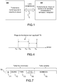
- the principle of message exchange used in the context of the invention is illustrated in the same temporal representation, the principle of message exchange used in the context of the invention. Note in the figure that there can be either synchronism or asynchronism of the message with the event itself.
- the message includes in particular as information, the date of the event and the description of the event itself.
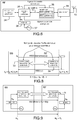
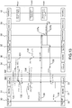
- the figure 3 represents an example of architecture according to the invention and shows the characteristic delays to be taken into account.
- the baseband part comprises, for example, a signal processing application module 30, or application BB which uses a local time or real time time H B , 31 to clock its operation. Local time is maintained by a local oscillator OL B , 32.
- the TS application module implements all of the functional and specific processing for the physical layer of a radio system.
- the application module can generate the messages intended for the radio subsystem chronologically or not.
- the application corresponds, for example, to the application that can be deployed in the SCA or SDR sense, or to the loadable application or rechargeable in classic architectures.
- the application manipulates one or more signals with minimum sampling frequency in a complex I / Q baseband format.
- the signal carried can however also be real (spectrum not centered on the zero frequency).
- the TS application of the BB in normal operation does not have to know the exact crossing times of the RF, but only the minimum and unique anticipation time to send a command to the RF; it is the RF module itself which is responsible for executing at the right time the command or commands necessary so that the action of the command can be performed at the right time on the antenna plane.
- the RF module therefore makes the necessary adjustment to the moment when the command or event is triggered, depending on the nature of the command or event and the physical implementation of the RF module.
- the signal and the commands from the signal processing application are transmitted to a generic interface controller 33, via encapsulation in formatted messages.
- the signals are dated messages MSG (H, [ei]) where the ei correspond to the series of samples to be sent. Orders are also dated messages. Examples will be given in the following description. The converse is identical in reception.
- the RF part comprises a generic interface controller 34 in connection with a module 35 for processing messages.
- the message processing module uses a local time or real time time H R , 36 supplied by a local oscillator 37, OL R.
- H R local time or real time time
- the message processing module 35 transforms the messages into digital control signals to the digital part 38 of the RF part and of the analog control signals to the analog part 39 of the RF part, and performs the extraction.
- IQ samples A transmitting antenna 10 transmits the signals associated with the radio application. The converse is identical in reception.
- the signal processing application module must operate in anticipation of the real-time time and must use a dated messaging system to exchange with the RF radio.
- the two sub-assemblies BB and RF forming the architecture according to the invention implement an hour function. Both subsets use the same format for the time.
- the baseband module will act as the time master with respect to the RF radio module which is a slave. Without departing from the scope of the invention, it is also possible to imagine an application in which, the radio module is time master and the application module is slave.
- the TS application operates with a minimum time anticipation value D A to be respected with respect to the real time time H B.
- a first part D R of the value D A is obtained from the RF itself, for example before the start of the application.
- This value D R is unique for each RF, or for each configuration that the RF is able to manage.
- a multi-band radio VHF / UHF
- D R corresponds to the maximum latency of the longest lasting RF radio frequency capacity.
- the second part of the anticipation value D I is obtained either by design of the hardware interface between the BB and the RF (constant), or by an explicit measurement of the transit time between the controller of the generic interface of the BB and the radio frequency module interface controller, performed during the system start-up phase.
- This value D I of transit time is unique for a given physical interconnection scheme.
- the values D R , D A , D I are deterministic values.
- the minimum anticipation delay D A with which the application will operate is obtained by the sum of D I + D R.
- the TS application In order to avoid a significant increase in the material resources of RF radio frequency, the TS application must also comply with a maximum anticipation period D M.
- the TS application can operate in an operating time window defined by [ D A , D M ] with respect to the real time H B , allowing it to de-constrain its dependence on RF, and to be able to operate in particular with time jitter.
- the application operating range of TS is shown on the figure 4 on a time axis.
- the sending of messages dated by the BB application to the RF will respect the minimum anticipation value D A.
- the messages received by the BB of the RF arrive with a delay D A ' whose value corresponds to the implementation of the system.
- This delay value is of the same order of magnitude as the minimum value D A but it can be different because the processing on the data path can be different.
- D A and D A ' correspond by design , for example, by making D A equal to Max ( D A and D A' ) .
- a packet of samples is to be sent before the current time ( HD A ) in a message whose completion date is H , that is to say that the first sample of the packet must be present at the output of antenna of the RF radio module at exactly H hour.
- a packet of samples is received at least after the completion time H, in a message whose completion date is H, that is to say that the first sample of the packet was acquired on the receiving antenna of the RF radio module exactly at the H hour.
- the expression “time of completion of a message” defines the date or time at which the RF module or sub-assembly should have performed an action described in the parameters of the message.
- the time for carrying out an order at the antenna level corresponds to the time of presentation of the data on the antenna plane.
- the figure 5 illustrates the operating principle of the TS application.
- the data to be transmitted 501 are transmitted to a processing chain comprising, for example, a channel coding module, followed by a modulation module, the coded and modulated signals are sent to a module suitable for inserting sequences of reference and then the signals are passed to a spectral shaping module.
- Control of the radio elements associated with the signal is also generated, containing the sampling frequency, the transmission time, the output power, the quantization of the samples, etc.
- Spectral shaping can be followed by an optional rendering chain.
- the radio control messages 502 originating from the transmission chain are dated and include the parameters which characterize the radio controls or the events.
- the I / Q samples, 503, to be sent are also in the form of dated messages.
- the TS application On reception, the TS application generates messages to control radio signal acquisitions and obtain IQ samples. These messages are of the outgoing type only, 505.
- the I / Q signal samples are received by the TS application in dated messages of the incoming type, 503. They are transmitted to a processing chain on reception comprising, for example, a acquisition chain, then a suitable filter, and to a synchronization module, then to an equalizer, the samples are then demodulated and then decoded.
- An output of the reception processing chain comprises the data received 504. Another output corresponds to the radio controls 505 which are in the form of dated messages.
- the TS signal processing application does not have to know the design elements of the RF module.
- the messages generated by the application to control the radio operation include the following parameters: the sampling frequency, the reception frequency, the reception time, the gain, etc.
- the RF part includes as in the figure 6 , a generic interface controller 34, of a module for processing messages 35 coming from the generic interface controller 34, which receives an hour H R coming from a TIME module 36 in connection with a local oscillator 37.
- the result messages processed at the output of the message processing module are control signals which aim to control the digital part 38 of the RF, control signals which will drive the analog part 39 of the RF part and IQ samples.
- the analog part receives the signals from the processing of the digital part and aims to perform the functions for transmitting the signals to the transmit-receive antenna 10 (and vice versa for reception).
- the digital part of the radio includes capacities for changing the sampling frequency up or down in frequency or DUC English acronym of Digital Up Converter / DDC 50 English acronym of Digital Down Converter adapted to interface with analog digital or ADC converters and analog digital or DAC converters.
- This function is not, in the context of the invention, recommended to be processed by the device BB.
- the principle is that the RF will carry out the adaptation at its level to avoid the dependencies of the application to the design of the conversion chain which is in the RF and which is therefore specific to it.
- the structure of the messages is important for unambiguously identifying the nature of the information contained in the messages.
- the architecture will therefore use a system of typing messages preferably systematic, unique and carried out message by message. Each message will carry a unique type value. Without departing from the scope of the invention, it will also be possible to create messages carrying several types, with consequently an extension of the duration of the messages and an extension of the latency of the exchanges.
- the figure 7 shows an example of a structure used for messages 70.
- the message consists, for example, of a first fixed part and a second part of variable size.
- the first part includes an address, 71, followed by the time 72 when a message is produced, the type 73 of the message, and the size of the data 74.
- the second part of variable size includes a field 75 of variable size for the data.
- the completion time can be deduced from the value H B if the message is sent from the BB, or from the value H R if the message is sent from the RF structure.
- the type of message can be: a single I / Q sample packet, multiple IQ sample packets (indication: start, in progress, stop), an RF configuration (time sync / maintenance, RF capabilities, etc.) .
- the size of the data corresponds to the number of data contained in the second data part.
- the sample packet exchanged between the part BB and the radio part will be segmented into several (n) messages m i , to optimize the required bit rate, only the first message m 1 , contains a date or time which will be used by the RF.
- the other messages m 2 , ... m n contain continuity or end of sequence information.
- the type of message enables segmentation, for example.
- variable quantification of the IQ samples makes it possible in particular to limit the bit rate on the generic link transmitting the messages. This makes it possible to process a wider frequency band when a large dynamic range is not required, which is the case when the automatic gain control AGC is performed on the RF side.
- the addressing and channel system allows all the flexibility necessary to be able to process SIMO / MIMO systems implemented using a single or multiple RF module.
- the figure 8 schematizes the loop made from the BB to calculate the transit time between the two generic interface controllers. To guarantee overall real-time operation, this delay must be taken into account.
- the transit time D I must be deterministic and reproducible. For example, the value of this delay can be measured at system start-up via the creation of a transmit / receive loop from the BB module.
- the loop is carried out from the BB and consists in sending a request message for the generation time of response of loop ⁇ to the RF. This time ⁇ corresponds to the time required for the RF to send its response back to the BB.
- the transit time D I is equal to [(t 0 -t 2 ) / 2] - ⁇ .
- the generic interface controller 33 (BB), or 34 (RF) must make it possible to synchronize the hours H B and H R. For this, it uses a specific message MSG (time [H B + D I ] sent from the BB, time master of the system, to the RF which plays a slave role. This message is sent by the BB to a precise time so that this message arrives exactly at the time of setting the time corresponding to the time message which it carries.
- the time H R of the RF is maintained identical to H B , thanks to periodic maintenance carried out by the interface controller 34.
- the maintenance procedure is, for example, carried out by exchanging dedicated periodic messages between the BB and the RF.
- the generic physical link is adapted to convey dated messages.
- the link is chosen according to, in particular, consumption constraints, the distance separating the BB and the RF and the bit rates necessary for the TS application. For example, to cover a complex sampling frequency range up to 20MHz, with 16-bit quantization, depending on the excess bit rate required by message headers, a bit rate of 640 Mbps is required.
- a large number of applications do not require more than 8 quantization bits, especially when the digital part of the RF supports the DUC / DDC function and the automatic gain control or AGC.
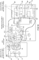
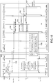
- the figure 10 is a functional block diagram of the elements implemented by the interface according to the invention. We find as in the figure 2 , at the level of the BB part, a local oscillator, a clock, a TS application and an interface controller. According to an alternative embodiment, it is possible to add an acquisition and restitution chain (DUC / DDC) known to those skilled in the art.
- DUC / DDC acquisition and restitution chain
- the RF part includes, for example, a generic interface controller 34, a message processing module, 35, a message anticipation table 101, a memory 102 for messages, a comparator module 103 which receives the different times, a time setting module 104, a clock, a local oscillator, a digital part comprising an analog / digital converter 105, a digital / analog converter 106, an analog part comprising a transmission channel 107 and a reception channel 108 in connection with the antenna 10.
- a generic interface controller 34 for example, a message processing module, 35, a message anticipation table 101, a memory 102 for messages, a comparator module 103 which receives the different times, a time setting module 104, a clock, a local oscillator, a digital part comprising an analog / digital converter 105, a digital / analog converter 106, an analog part comprising a transmission channel 107 and a reception channel 108 in connection with the antenna 10.
- the message processing module is adapted to execute the messages received from the BB and to generate messages to build and send to the BB.
- This module notably has the function of controlling the entire RF part and it guarantees real-time compliance.
- This module interprets the messages received from the BB, in particular the hours of application of the messages. It uses local time H R in order to anticipate the execution of the message. It generates all the internal control signals of the RF module aimed at setting up digital and analog processing.
- This module includes all of the real-time sequencing functions. It generates all of the discrete signals used for the necessary settings and checks.
- the digital part of the RF notably includes a set of modules adapted for the digital treatments of the RF detailed in the figure 11 .
- the purpose of these modules is in particular to support specific processing of the radio design and to allow the proper execution of the messages.
- the processing performed at the digital part of the RF is controlled by the message processing sequencer module.
- the I / Q samples of the message at the output of the message processing sequencer are transmitted, for example, to a DUC module in order to manage the rise in the sampling frequency of the DAC, then the samples pass into a power management module d 'emission (automatic level control or ALC: Automatic Level Control), before being modulated and converted within the CNA.
- a DUC module in order to manage the rise in the sampling frequency of the DAC
- ALC Automatic Level Control
- the analog signal received on the receiving antenna is converted into digital samples which are demodulated to obtain the I / Q samples.
- the I / Q samples are then transmitted to a CAG transmission power management module, the next step being to control the descent at the sampling frequency in the DDC module.
- the RF part includes all of the analog processing known to those skilled in the art between the input / output of the CAN / DAC and the transmit / receive antenna. These treatments are controlled by the sequencer module processing messages which transmits to the analog part of RF analog control signals. As analog treatments which will not be detailed in the description, it is possible to cite, filtering, power amplifier or PA (acronym acronym for Power Amplifier), switches, transposition, low noise amplifier or LNA (acronym for Low Noise Amplifier), etc.
- the figure 12 shows an example of the sequence of steps performed by the method according to the invention.
- the BB which in this example is the system master, performs the initializations necessary for time control with the RF.
- the BB requests, 120, from the RF the value of the delay ⁇ necessary for the BB to calculate the delay D I of the interface between BB and RF.
- the RF provides it with 121 this value.
- the BB then performs the configuration of the RF, 122, according to the desired operating mode and obtains, in return, 123, the value D R allowing the BB to calculate the anticipation delay D A with which the TS application must operate. .
- the TS application starts its activity. This activity consists in exchanging dated messages MSG (H I ) indicating to the RF the processing to be carried out.
- a waveform with N S jumps per second is considered, corresponding to the duration T P between each start of transmissions.
- the first message transmitted, by the message carrying the time H 5 indicates the frequency f 0 and the transmission power P TX to be used at the time H 5 .
- This message is used to order the RF configurations for the hour H 5 .
- the second message bearing the time H 5 contains the IQ samples to be sent at the time H 5 . These samples are consistent with the configuration sent during the previous message for the hour H 5 . The order and sequencing of these messages does not matter except for the anticipation constraint described below.
- the messages sent by the BB to the RF party are all sent with an anticipation of value D A , and are not necessarily synchronous of the antenna instants.
- the messages are not strictly spaced from T P , and they can be sent either during the previous level, or even two levels in advance, for example, the command of the level Tx on H 8 is sent two levels in advance .
- the messages are asynchronous with the operation of the RF.
- each level is indeed transmitted at the desired times (H 5 , H 6 , H 7 , H 8 ) and the signals transmitted or received have a duration of nF S , where n is the number of samples and F S the frequency duration, which corresponds to the actual duration of the samples.
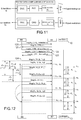
- the figure 13 shows an example of the sequence of steps involved when starting the system. There are three phases to starting the system, for example.
- the delay in crossing the interface between BB and RF is determined, then during the second phase, the hours of the BB and the RF are synchronized, then during the third phase, the BB configure RF and recovers the minimum RF anticipation delay.
- the method will carry out a transmission / reception loop between the interface controller BB and the RF interface controller.
- the interface controller BB sends an MSG message (request ( ⁇ )) to the RF interface controller in order to recover the time necessary on the RF side to manufacture, 131, the return message MSG ( ⁇ ) which contains the delay ⁇ .
- the manufacturing and message reception times on the BB side are not necessarily essential because if they are equal, their contributions cancel each other out. If they are different, their individual contributions are known and can be taken into account.
- the BB transmits at time H B , 133, an MSG message (time setting [H B + D I ]) to the RF containing the time H B increased by the interface delay D I , time required to route the message to the time module on the RF side.
- an MSG message time setting [H B + D I ]
- the TS application sends, 136, by an MSG message (RF Config) all the configurations and / or configuration information necessary for its operation, declined by the RF in digital configuration 137a and in analog configuration 137b.
- MSG message RF Config
- the RF returns 138, an MSG message (D R ) containing the duration of anticipation D R necessary for the processing of the messages which are intended for it.
- This minimum anticipation D A is respected by the application TS to communicate with the RF.
- the BB will request the transmission of IQ sample packets, figure 14 .
- the TS application acquires the current time from the time module. It then determines, 141, according to its own needs, the time H TX at which it wishes to see the signal coming out at the foot of the antenna, corresponding to the first sample of the packet which it has or which it will generate.
- the application TS sends two messages 142a, 142b, before the date or instant H TX -D A to the RF.
- the times ⁇ 1 and ⁇ 2 on the diagram represent the time anticipation before H TX -D A that the application TS takes to generate the messages 142a and 142b.
- the first message corresponds to the order of transition to transmission from time H TX , with the desired configuration of the RF (for example, the transmission power, the carrier frequency, etc.), the second message corresponds IQ samples that are associated with this configuration.
- the messages are routed by the BB interface controllers to the RF and are immediately stored, 143a, 143b, in the memory of the RF.
- the message processing module 35 also immediately determines the temporary storage times for each of the two messages before launching their executions. The storage times can be different depending on the TYPE of messages.
- the message processing module When the temporary storage times are over, the message processing module performs the execution of the messages: it performs the digital 145 and analog 146 configurations of the RF, then activates, 147, the flow of IQ sample data which is then routed 148 to the antenna base in absolute respect of real time.
- the figure 15 illustrates the steps implemented for the reception of an IQ sample packet with associated RF configuration.
- the reception of a packet of IQ samples is requested by the BB.
- the TS application acquires, 151, the current time from the TIME module. It then determines, according to its own needs, the hour H RX , 152, at which it wishes to acquire the signal at the base of the antenna which will correspond to the first sample of the packet which it will receive.
- This message corresponds to the order of taking into account the first sample Rx from time H RX , with the desired configuration of the RF (Gain, carrier frequency, etc.).
- the message is routed by the BB's interface controllers to the RF and is immediately stored, 154, in the memory of the RF.
- the message processing module immediately determines the temporary storage time for this message before starting its execution.
- the message processing module executes the messages: it performs the digital 155, and analog 156, RF configurations, then activates 157 the data path from the antenna base, to the digital output which provides IQ sample data in absolute respect of real time.
- An MSG message (H RX , IQ, n, [r 1 , .. r n ]) is then generated, 158, in the RF, containing exactly the instant H RX , corresponding to the first sample of the packet, and the IQ samples associated.
- This message is then routed to the BB by the RF interface controller and the BB interface controller.
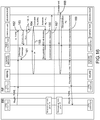
- the figure 16 illustrates how message processing works.
- the chronogram of the figure 16 details the internal sequences of the “message processing” module of the three previous diagrams ( figures 13 , 14 and 15 ). Two cases are to be considered: messages generated by the BB, and messages generated by the RF.
- the comparator consults, 163, (request to MSG ) the anticipation table which contains the processing times necessary for the RF and corresponding to each type of message. It then calculates, 164, the instant of completion H S , corresponding to the instant of triggering of the processing module (Sequencer) which will execute the message. The comparator then compares, 165, the date of realization H S with the current time H R , and when equality occurs, the data corresponding to the message from the memory is recovered 166 and the execution of the message starts 167.
- the transmission of a message from the RF to the BB is conditioned by the appearance of an event, 168.
- the event corresponds to the instant acquisition at the antenna base, corresponding to the first IQ sample.
- the message processing module or sequencer acquires the current time after the TIME module.
- the sequencer builds the message by placing the time of the event, the type of message and the IQ samples, which it sends, 169, opportunistically as quickly as possible to the BB.
- the sampling frequency and the size of the packets it is conceivable that the instant of sending the message occurs before the end of reception of the last sample of the packet.
- BB Baseband
- RF radiofrequency
- the baseband and radio frequency sub-assemblies communicate via dated message exchanges which allow them to understand each other logically.
- the dates indicating the moments of realization of the events (configuration, emission or reception), the BB and RF subsets can operate in an asynchronous manner, which allows to decorrelate the real-time constraints.
- the exchange of messages also makes it possible to dispense with precise knowledge of the capacities supported by radio frequency and the associated performances.
- the software implemented in the baseband part is independent of the radio frequency part.
- the sub-assemblies thus defined can be reused directly with other modules of different design but respecting the same architectural framework.
- the method does not issue any constraint on the type (technology / architecture) of the memory 102 to be used. It does not require the TS application 30 to generate chronically the messages intended for the RF, nor to the RF to have to sort the contents of the memory 102 containing the messages.
Landscapes
- Engineering & Computer Science (AREA)
- Computer Networks & Wireless Communication (AREA)
- Signal Processing (AREA)
- Power Engineering (AREA)
- Mobile Radio Communication Systems (AREA)
- Transceivers (AREA)
Priority Applications (1)
| Application Number | Priority Date | Filing Date | Title |
|---|---|---|---|
| PL14715866T PL2979378T3 (pl) | 2013-03-27 | 2014-03-27 | Struktura interfejsu między podzespołem cyfrowym i podzespołem radiowym |
Applications Claiming Priority (2)
| Application Number | Priority Date | Filing Date | Title |
|---|---|---|---|
| FR1300710A FR3004038B1 (fr) | 2013-03-27 | 2013-03-27 | Architecture d'interface entre sous ensembles numerique et radio. |
| PCT/EP2014/056193 WO2014154821A1 (fr) | 2013-03-27 | 2014-03-27 | Architecture d'interface entre sous ensembles numerique et radio |
Publications (2)
| Publication Number | Publication Date |
|---|---|
| EP2979378A1 EP2979378A1 (fr) | 2016-02-03 |
| EP2979378B1 true EP2979378B1 (fr) | 2020-04-22 |
Family
ID=48901030
Family Applications (1)
| Application Number | Title | Priority Date | Filing Date |
|---|---|---|---|
| EP14715866.1A Active EP2979378B1 (fr) | 2013-03-27 | 2014-03-27 | Architecture d'interface entre sous ensembles numerique et radio |
Country Status (10)
| Country | Link |
|---|---|
| US (1) | US9496898B2 (pl) |
| EP (1) | EP2979378B1 (pl) |
| DK (1) | DK2979378T3 (pl) |
| ES (1) | ES2807376T3 (pl) |
| FR (1) | FR3004038B1 (pl) |
| HU (1) | HUE051371T2 (pl) |
| MY (1) | MY172096A (pl) |
| PL (1) | PL2979378T3 (pl) |
| SG (1) | SG11201508044XA (pl) |
| WO (1) | WO2014154821A1 (pl) |
Families Citing this family (3)
| Publication number | Priority date | Publication date | Assignee | Title |
|---|---|---|---|---|
| KR102595903B1 (ko) | 2016-08-26 | 2023-10-30 | 삼성전자주식회사 | 모뎀 칩, 이를 포함하는 어플리케이션 프로세서 및 모뎀 칩의 동작방법 |
| US10999054B2 (en) * | 2018-12-21 | 2021-05-04 | Motorola Solutions, Inc. | Method for synchronizing radio frequency carrier correction of dynamic radio frequency carriers |
| US12299325B2 (en) * | 2020-09-25 | 2025-05-13 | Micron Technology, Inc. | Frequency monitoring for memory devices |
Family Cites Families (9)
| Publication number | Priority date | Publication date | Assignee | Title |
|---|---|---|---|---|
| JP3180735B2 (ja) | 1997-10-22 | 2001-06-25 | 松下電器産業株式会社 | 送信タイミング補正機能付き無線端末及びその製造方法 |
| US7664532B2 (en) * | 2006-06-02 | 2010-02-16 | Nokia Corporation | Radio transmission scheduling according to multiradio control in a radio modem |
| US8321489B2 (en) * | 2006-09-15 | 2012-11-27 | National Semiconductor Corporation | Software reconfigurable digital phase lock loop architecture |
| US7948964B1 (en) * | 2006-12-14 | 2011-05-24 | Rf Micro Devices, Inc. | Synchronizing a radio frequency transmit message with an asynchronous radio frequency receive message |
| GB0709813D0 (en) * | 2007-05-22 | 2007-07-04 | Nokia Corp | A radio frequency apparatus |
| EP2068250B1 (en) * | 2007-06-08 | 2016-02-17 | Motorola Mobility LLC | Method and apparatuses for communicating a message received from a main processor to a peripheral device |
| EP2107684A1 (en) * | 2008-03-31 | 2009-10-07 | Telefonaktiebolaget LM Ericsson (publ) | Event handling in a radio circuit |
| EP2154788B1 (en) * | 2008-08-12 | 2017-06-28 | Nxp B.V. | Time accurate control of RF over a DigRF interface |
| US9136894B2 (en) * | 2012-04-30 | 2015-09-15 | Hewlett-Packard Development Company, L.P. | Hybrid platform for a software defined radio |
-
2013
- 2013-03-27 FR FR1300710A patent/FR3004038B1/fr not_active Expired - Fee Related
-
2014
- 2014-03-27 WO PCT/EP2014/056193 patent/WO2014154821A1/fr not_active Ceased
- 2014-03-27 US US14/780,546 patent/US9496898B2/en active Active
- 2014-03-27 ES ES14715866T patent/ES2807376T3/es active Active
- 2014-03-27 MY MYPI2015002452A patent/MY172096A/en unknown
- 2014-03-27 SG SG11201508044XA patent/SG11201508044XA/en unknown
- 2014-03-27 EP EP14715866.1A patent/EP2979378B1/fr active Active
- 2014-03-27 DK DK14715866.1T patent/DK2979378T3/da active
- 2014-03-27 HU HUE14715866A patent/HUE051371T2/hu unknown
- 2014-03-27 PL PL14715866T patent/PL2979378T3/pl unknown
Non-Patent Citations (1)
| Title |
|---|
| None * |
Also Published As
| Publication number | Publication date |
|---|---|
| SG11201508044XA (en) | 2015-11-27 |
| MY172096A (en) | 2019-11-13 |
| US20160056844A1 (en) | 2016-02-25 |
| DK2979378T3 (da) | 2020-08-03 |
| ES2807376T3 (es) | 2021-02-22 |
| PL2979378T3 (pl) | 2020-10-19 |
| HUE051371T2 (hu) | 2021-03-01 |
| FR3004038A1 (fr) | 2014-10-03 |
| US9496898B2 (en) | 2016-11-15 |
| WO2014154821A1 (fr) | 2014-10-02 |
| FR3004038B1 (fr) | 2016-11-11 |
| EP2979378A1 (fr) | 2016-02-03 |
Similar Documents
| Publication | Publication Date | Title |
|---|---|---|
| EP0812080A1 (fr) | Dispositif autonome, notamment dispositif médical implantable actif, et son programmateur externe à transmission synchrone | |
| WO2011009707A1 (fr) | Procede et systeme de synchronisation de haute precision | |
| EP2979378B1 (fr) | Architecture d'interface entre sous ensembles numerique et radio | |
| CA3053707A1 (fr) | Procede et systeme de synchronisation | |
| EP0816866A1 (fr) | Procédé d'analyse spectrale, notamment pour radioaltimétre de type FM/CW à traitement numérique | |
| EP4033680A1 (fr) | Procédé de synchronisation de domaines temporels d'un système sur puce | |
| EP3633876B1 (fr) | Système de traitement et d'observation pour la mise en oeuvre de l'observation de la terre, architecture d'observation et procédé d'observation associés | |
| FR3044104B1 (fr) | Recepteur pour systeme de positionnement par satellites et procede de traitement de signaux satellites | |
| CN115796291A (zh) | 信号同步方法、装置、电子设备及计算机可读存储介质 | |
| FR3133508A1 (fr) | Dispositif comportant un circuit de synchronisation pour realiser une communication en champ proche | |
| WO2023089278A1 (fr) | Procédé et équipements associés de synchronisation d'un système de télétransmission de données sans fil | |
| FR3041845A1 (fr) | Dispositif electronique propre a etre relie a un reseau de vehicule, et procede de transmission de messages mis en oeuvre par un tel dispositif electronique | |
| EP3469986B1 (fr) | Procede de synchronisation d'un systeme de localisation magnetique | |
| EP3888333A1 (fr) | Activation ou désactivation d'un sous-ensemble virtuel d'un réseau dédié à un service pour un terminal | |
| CN111812643B (zh) | 一种雷达成像方法、装置、设备及存储介质 | |
| WO2009071568A1 (fr) | Dispositif de resynchronisation de signaux analogiques obtenus par conversion, avec des convertisseurs numerique-analogique ddr, de signaux numeriques synchronises | |
| EP3391695B1 (fr) | Procédé de gestion du fonctionnement d'un objet connecté | |
| FR3013925A1 (fr) | Procede et dispositif de synchronisation d'une horloge d'un systeme informatique, a partir d'une source de temps reseau, via une interface de gestion | |
| EP2866365B1 (fr) | Procédé et système de synchronisation horaire entre deux dispositifs connectés par une liaison Ethernet | |
| EP1411638A1 (fr) | Procédé et dispositif de génération d'un signal ayant une fréquence égale au produit d'une fréquence de référence par un nombre réel | |
| EP2728909A1 (fr) | Procédé d' obtention d'échantillons numerises de signaux radio, procédé de traitement d' une requête de recherche d'échantillons, procédé de traitement de signaux radio, dispositifs et équipements associés | |
| FR2836612A1 (fr) | Procede de transmission de donnees numeriques au moyen d'un modulateur de frequence et modulateur correspondant | |
| WO2015097408A1 (fr) | Synchronisation des communications dans une installation de telereleve | |
| FR3103035A1 (fr) | Procédé de réglage d’une horloge embarquée dans un véhicule automobile et dispositif de réglage associé | |
| FR3140231A1 (fr) | Procédé de détermination du déphasage entre un premier signal d’horloge reçu par un premier composant électronique et un deuxième signal d’horloge reçu par un deuxième composant électronique |
Legal Events
| Date | Code | Title | Description |
|---|---|---|---|
| PUAI | Public reference made under article 153(3) epc to a published international application that has entered the european phase |
Free format text: ORIGINAL CODE: 0009012 |
|
| 17P | Request for examination filed |
Effective date: 20151009 |
|
| AK | Designated contracting states |
Kind code of ref document: A1 Designated state(s): AL AT BE BG CH CY CZ DE DK EE ES FI FR GB GR HR HU IE IS IT LI LT LU LV MC MK MT NL NO PL PT RO RS SE SI SK SM TR |
|
| AX | Request for extension of the european patent |
Extension state: BA ME |
|
| DAX | Request for extension of the european patent (deleted) | ||
| GRAP | Despatch of communication of intention to grant a patent |
Free format text: ORIGINAL CODE: EPIDOSNIGR1 |
|
| STAA | Information on the status of an ep patent application or granted ep patent |
Free format text: STATUS: GRANT OF PATENT IS INTENDED |
|
| INTG | Intention to grant announced |
Effective date: 20190705 |
|
| GRAJ | Information related to disapproval of communication of intention to grant by the applicant or resumption of examination proceedings by the epo deleted |
Free format text: ORIGINAL CODE: EPIDOSDIGR1 |
|
| STAA | Information on the status of an ep patent application or granted ep patent |
Free format text: STATUS: REQUEST FOR EXAMINATION WAS MADE |
|
| GRAP | Despatch of communication of intention to grant a patent |
Free format text: ORIGINAL CODE: EPIDOSNIGR1 |
|
| STAA | Information on the status of an ep patent application or granted ep patent |
Free format text: STATUS: GRANT OF PATENT IS INTENDED |
|
| INTC | Intention to grant announced (deleted) | ||
| INTG | Intention to grant announced |
Effective date: 20191120 |
|
| GRAS | Grant fee paid |
Free format text: ORIGINAL CODE: EPIDOSNIGR3 |
|
| GRAA | (expected) grant |
Free format text: ORIGINAL CODE: 0009210 |
|
| STAA | Information on the status of an ep patent application or granted ep patent |
Free format text: STATUS: THE PATENT HAS BEEN GRANTED |
|
| AK | Designated contracting states |
Kind code of ref document: B1 Designated state(s): AL AT BE BG CH CY CZ DE DK EE ES FI FR GB GR HR HU IE IS IT LI LT LU LV MC MK MT NL NO PL PT RO RS SE SI SK SM TR |
|
| REG | Reference to a national code |
Ref country code: CH Ref legal event code: EP |
|
| REG | Reference to a national code |
Ref country code: IE Ref legal event code: FG4D Free format text: LANGUAGE OF EP DOCUMENT: FRENCH |
|
| REG | Reference to a national code |
Ref country code: DE Ref legal event code: R096 Ref document number: 602014064082 Country of ref document: DE |
|
| REG | Reference to a national code |
Ref country code: AT Ref legal event code: REF Ref document number: 1261527 Country of ref document: AT Kind code of ref document: T Effective date: 20200515 |
|
| REG | Reference to a national code |
Ref country code: FI Ref legal event code: FGE |
|
| REG | Reference to a national code |
Ref country code: DK Ref legal event code: T3 Effective date: 20200728 |
|
| REG | Reference to a national code |
Ref country code: NL Ref legal event code: FP |
|
| REG | Reference to a national code |
Ref country code: NO Ref legal event code: T2 Effective date: 20200422 |
|
| REG | Reference to a national code |
Ref country code: LT Ref legal event code: MG4D |
|
| PG25 | Lapsed in a contracting state [announced via postgrant information from national office to epo] |
Ref country code: LT Free format text: LAPSE BECAUSE OF FAILURE TO SUBMIT A TRANSLATION OF THE DESCRIPTION OR TO PAY THE FEE WITHIN THE PRESCRIBED TIME-LIMIT Effective date: 20200422 Ref country code: PT Free format text: LAPSE BECAUSE OF FAILURE TO SUBMIT A TRANSLATION OF THE DESCRIPTION OR TO PAY THE FEE WITHIN THE PRESCRIBED TIME-LIMIT Effective date: 20200824 Ref country code: GR Free format text: LAPSE BECAUSE OF FAILURE TO SUBMIT A TRANSLATION OF THE DESCRIPTION OR TO PAY THE FEE WITHIN THE PRESCRIBED TIME-LIMIT Effective date: 20200723 Ref country code: IS Free format text: LAPSE BECAUSE OF FAILURE TO SUBMIT A TRANSLATION OF THE DESCRIPTION OR TO PAY THE FEE WITHIN THE PRESCRIBED TIME-LIMIT Effective date: 20200822 Ref country code: SE Free format text: LAPSE BECAUSE OF FAILURE TO SUBMIT A TRANSLATION OF THE DESCRIPTION OR TO PAY THE FEE WITHIN THE PRESCRIBED TIME-LIMIT Effective date: 20200422 |
|
| REG | Reference to a national code |
Ref country code: AT Ref legal event code: MK05 Ref document number: 1261527 Country of ref document: AT Kind code of ref document: T Effective date: 20200422 |
|
| PG25 | Lapsed in a contracting state [announced via postgrant information from national office to epo] |
Ref country code: HR Free format text: LAPSE BECAUSE OF FAILURE TO SUBMIT A TRANSLATION OF THE DESCRIPTION OR TO PAY THE FEE WITHIN THE PRESCRIBED TIME-LIMIT Effective date: 20200422 Ref country code: BG Free format text: LAPSE BECAUSE OF FAILURE TO SUBMIT A TRANSLATION OF THE DESCRIPTION OR TO PAY THE FEE WITHIN THE PRESCRIBED TIME-LIMIT Effective date: 20200722 Ref country code: RS Free format text: LAPSE BECAUSE OF FAILURE TO SUBMIT A TRANSLATION OF THE DESCRIPTION OR TO PAY THE FEE WITHIN THE PRESCRIBED TIME-LIMIT Effective date: 20200422 Ref country code: LV Free format text: LAPSE BECAUSE OF FAILURE TO SUBMIT A TRANSLATION OF THE DESCRIPTION OR TO PAY THE FEE WITHIN THE PRESCRIBED TIME-LIMIT Effective date: 20200422 |
|
| PG25 | Lapsed in a contracting state [announced via postgrant information from national office to epo] |
Ref country code: AL Free format text: LAPSE BECAUSE OF FAILURE TO SUBMIT A TRANSLATION OF THE DESCRIPTION OR TO PAY THE FEE WITHIN THE PRESCRIBED TIME-LIMIT Effective date: 20200422 |
|
| REG | Reference to a national code |
Ref country code: DE Ref legal event code: R097 Ref document number: 602014064082 Country of ref document: DE |
|
| PG25 | Lapsed in a contracting state [announced via postgrant information from national office to epo] |
Ref country code: AT Free format text: LAPSE BECAUSE OF FAILURE TO SUBMIT A TRANSLATION OF THE DESCRIPTION OR TO PAY THE FEE WITHIN THE PRESCRIBED TIME-LIMIT Effective date: 20200422 Ref country code: EE Free format text: LAPSE BECAUSE OF FAILURE TO SUBMIT A TRANSLATION OF THE DESCRIPTION OR TO PAY THE FEE WITHIN THE PRESCRIBED TIME-LIMIT Effective date: 20200422 Ref country code: SM Free format text: LAPSE BECAUSE OF FAILURE TO SUBMIT A TRANSLATION OF THE DESCRIPTION OR TO PAY THE FEE WITHIN THE PRESCRIBED TIME-LIMIT Effective date: 20200422 Ref country code: RO Free format text: LAPSE BECAUSE OF FAILURE TO SUBMIT A TRANSLATION OF THE DESCRIPTION OR TO PAY THE FEE WITHIN THE PRESCRIBED TIME-LIMIT Effective date: 20200422 |
|
| REG | Reference to a national code |
Ref country code: ES Ref legal event code: FG2A Ref document number: 2807376 Country of ref document: ES Kind code of ref document: T3 Effective date: 20210222 |
|
| PG25 | Lapsed in a contracting state [announced via postgrant information from national office to epo] |
Ref country code: SK Free format text: LAPSE BECAUSE OF FAILURE TO SUBMIT A TRANSLATION OF THE DESCRIPTION OR TO PAY THE FEE WITHIN THE PRESCRIBED TIME-LIMIT Effective date: 20200422 |
|
| PLBE | No opposition filed within time limit |
Free format text: ORIGINAL CODE: 0009261 |
|
| STAA | Information on the status of an ep patent application or granted ep patent |
Free format text: STATUS: NO OPPOSITION FILED WITHIN TIME LIMIT |
|
| REG | Reference to a national code |
Ref country code: HU Ref legal event code: AG4A Ref document number: E051371 Country of ref document: HU |
|
| 26N | No opposition filed |
Effective date: 20210125 |
|
| PG25 | Lapsed in a contracting state [announced via postgrant information from national office to epo] |
Ref country code: SI Free format text: LAPSE BECAUSE OF FAILURE TO SUBMIT A TRANSLATION OF THE DESCRIPTION OR TO PAY THE FEE WITHIN THE PRESCRIBED TIME-LIMIT Effective date: 20200422 |
|
| PG25 | Lapsed in a contracting state [announced via postgrant information from national office to epo] |
Ref country code: MC Free format text: LAPSE BECAUSE OF FAILURE TO SUBMIT A TRANSLATION OF THE DESCRIPTION OR TO PAY THE FEE WITHIN THE PRESCRIBED TIME-LIMIT Effective date: 20200422 |
|
| REG | Reference to a national code |
Ref country code: CH Ref legal event code: PL |
|
| GBPC | Gb: european patent ceased through non-payment of renewal fee |
Effective date: 20210327 |
|
| PG25 | Lapsed in a contracting state [announced via postgrant information from national office to epo] |
Ref country code: CH Free format text: LAPSE BECAUSE OF NON-PAYMENT OF DUE FEES Effective date: 20210331 Ref country code: LI Free format text: LAPSE BECAUSE OF NON-PAYMENT OF DUE FEES Effective date: 20210331 Ref country code: GB Free format text: LAPSE BECAUSE OF NON-PAYMENT OF DUE FEES Effective date: 20210327 |
|
| P01 | Opt-out of the competence of the unified patent court (upc) registered |
Effective date: 20230517 |
|
| PG25 | Lapsed in a contracting state [announced via postgrant information from national office to epo] |
Ref country code: CY Free format text: LAPSE BECAUSE OF FAILURE TO SUBMIT A TRANSLATION OF THE DESCRIPTION OR TO PAY THE FEE WITHIN THE PRESCRIBED TIME-LIMIT Effective date: 20200422 |
|
| PG25 | Lapsed in a contracting state [announced via postgrant information from national office to epo] |
Ref country code: MK Free format text: LAPSE BECAUSE OF FAILURE TO SUBMIT A TRANSLATION OF THE DESCRIPTION OR TO PAY THE FEE WITHIN THE PRESCRIBED TIME-LIMIT Effective date: 20200422 |
|
| PG25 | Lapsed in a contracting state [announced via postgrant information from national office to epo] |
Ref country code: MT Free format text: LAPSE BECAUSE OF FAILURE TO SUBMIT A TRANSLATION OF THE DESCRIPTION OR TO PAY THE FEE WITHIN THE PRESCRIBED TIME-LIMIT Effective date: 20200422 |
|
| PGFP | Annual fee paid to national office [announced via postgrant information from national office to epo] |
Ref country code: DE Payment date: 20250218 Year of fee payment: 12 |
|
| PGFP | Annual fee paid to national office [announced via postgrant information from national office to epo] |
Ref country code: DK Payment date: 20250317 Year of fee payment: 12 Ref country code: FI Payment date: 20250314 Year of fee payment: 12 |
|
| PGFP | Annual fee paid to national office [announced via postgrant information from national office to epo] |
Ref country code: LU Payment date: 20250313 Year of fee payment: 12 |
|
| PGFP | Annual fee paid to national office [announced via postgrant information from national office to epo] |
Ref country code: HU Payment date: 20250305 Year of fee payment: 12 |
|
| PGFP | Annual fee paid to national office [announced via postgrant information from national office to epo] |
Ref country code: IE Payment date: 20250224 Year of fee payment: 12 |
|
| PGFP | Annual fee paid to national office [announced via postgrant information from national office to epo] |
Ref country code: NO Payment date: 20250312 Year of fee payment: 12 |
|
| PGFP | Annual fee paid to national office [announced via postgrant information from national office to epo] |
Ref country code: BE Payment date: 20250214 Year of fee payment: 12 |
|
| PGFP | Annual fee paid to national office [announced via postgrant information from national office to epo] |
Ref country code: FR Payment date: 20250224 Year of fee payment: 12 Ref country code: PL Payment date: 20250218 Year of fee payment: 12 Ref country code: CZ Payment date: 20250304 Year of fee payment: 12 |
|
| PGFP | Annual fee paid to national office [announced via postgrant information from national office to epo] |
Ref country code: IT Payment date: 20250226 Year of fee payment: 12 |
|
| PGFP | Annual fee paid to national office [announced via postgrant information from national office to epo] |
Ref country code: ES Payment date: 20250410 Year of fee payment: 12 |
|
| PG25 | Lapsed in a contracting state [announced via postgrant information from national office to epo] |
Ref country code: TR Free format text: LAPSE BECAUSE OF FAILURE TO SUBMIT A TRANSLATION OF THE DESCRIPTION OR TO PAY THE FEE WITHIN THE PRESCRIBED TIME-LIMIT Effective date: 20200422 |
|
| PGFP | Annual fee paid to national office [announced via postgrant information from national office to epo] |
Ref country code: NL Payment date: 20260227 Year of fee payment: 13 |