EP2978013A1 - Semiconductor device - Google Patents
Semiconductor device Download PDFInfo
- Publication number
- EP2978013A1 EP2978013A1 EP13878857.5A EP13878857A EP2978013A1 EP 2978013 A1 EP2978013 A1 EP 2978013A1 EP 13878857 A EP13878857 A EP 13878857A EP 2978013 A1 EP2978013 A1 EP 2978013A1
- Authority
- EP
- European Patent Office
- Prior art keywords
- layer
- doped
- semiconductor device
- inalas
- electron supply
- Prior art date
- Legal status (The legal status is an assumption and is not a legal conclusion. Google has not performed a legal analysis and makes no representation as to the accuracy of the status listed.)
- Withdrawn
Links
Images







Classifications
-
- H—ELECTRICITY
- H10—SEMICONDUCTOR DEVICES; ELECTRIC SOLID-STATE DEVICES NOT OTHERWISE PROVIDED FOR
- H10D—INORGANIC ELECTRIC SEMICONDUCTOR DEVICES
- H10D62/00—Semiconductor bodies, or regions thereof, of devices having potential barriers
- H10D62/80—Semiconductor bodies, or regions thereof, of devices having potential barriers characterised by the materials
- H10D62/82—Heterojunctions
- H10D62/824—Heterojunctions comprising only Group III-V materials heterojunctions, e.g. GaN/AlGaN heterojunctions
-
- H—ELECTRICITY
- H10—SEMICONDUCTOR DEVICES; ELECTRIC SOLID-STATE DEVICES NOT OTHERWISE PROVIDED FOR
- H10D—INORGANIC ELECTRIC SEMICONDUCTOR DEVICES
- H10D30/00—Field-effect transistors [FET]
- H10D30/01—Manufacture or treatment
- H10D30/015—Manufacture or treatment of FETs having heterojunction interface channels or heterojunction gate electrodes, e.g. HEMT
-
- H—ELECTRICITY
- H10—SEMICONDUCTOR DEVICES; ELECTRIC SOLID-STATE DEVICES NOT OTHERWISE PROVIDED FOR
- H10D—INORGANIC ELECTRIC SEMICONDUCTOR DEVICES
- H10D30/00—Field-effect transistors [FET]
- H10D30/40—FETs having zero-dimensional [0D], one-dimensional [1D] or two-dimensional [2D] charge carrier gas channels
- H10D30/47—FETs having zero-dimensional [0D], one-dimensional [1D] or two-dimensional [2D] charge carrier gas channels having two-dimensional [2D] charge carrier gas channels, e.g. nanoribbon FETs or high electron mobility transistors [HEMT]
-
- H—ELECTRICITY
- H10—SEMICONDUCTOR DEVICES; ELECTRIC SOLID-STATE DEVICES NOT OTHERWISE PROVIDED FOR
- H10D—INORGANIC ELECTRIC SEMICONDUCTOR DEVICES
- H10D30/00—Field-effect transistors [FET]
- H10D30/40—FETs having zero-dimensional [0D], one-dimensional [1D] or two-dimensional [2D] charge carrier gas channels
- H10D30/47—FETs having zero-dimensional [0D], one-dimensional [1D] or two-dimensional [2D] charge carrier gas channels having two-dimensional [2D] charge carrier gas channels, e.g. nanoribbon FETs or high electron mobility transistors [HEMT]
- H10D30/471—High electron mobility transistors [HEMT] or high hole mobility transistors [HHMT]
- H10D30/473—High electron mobility transistors [HEMT] or high hole mobility transistors [HHMT] having confinement of carriers by multiple heterojunctions, e.g. quantum well HEMT
- H10D30/4732—High electron mobility transistors [HEMT] or high hole mobility transistors [HHMT] having confinement of carriers by multiple heterojunctions, e.g. quantum well HEMT using Group III-V semiconductor material
- H10D30/4735—High electron mobility transistors [HEMT] or high hole mobility transistors [HHMT] having confinement of carriers by multiple heterojunctions, e.g. quantum well HEMT using Group III-V semiconductor material having delta-doped or planar-doped donor layers
-
- H—ELECTRICITY
- H10—SEMICONDUCTOR DEVICES; ELECTRIC SOLID-STATE DEVICES NOT OTHERWISE PROVIDED FOR
- H10D—INORGANIC ELECTRIC SEMICONDUCTOR DEVICES
- H10D30/00—Field-effect transistors [FET]
- H10D30/40—FETs having zero-dimensional [0D], one-dimensional [1D] or two-dimensional [2D] charge carrier gas channels
- H10D30/47—FETs having zero-dimensional [0D], one-dimensional [1D] or two-dimensional [2D] charge carrier gas channels having two-dimensional [2D] charge carrier gas channels, e.g. nanoribbon FETs or high electron mobility transistors [HEMT]
- H10D30/471—High electron mobility transistors [HEMT] or high hole mobility transistors [HHMT]
- H10D30/475—High electron mobility transistors [HEMT] or high hole mobility transistors [HHMT] having wider bandgap layer formed on top of lower bandgap active layer, e.g. undoped barrier HEMTs such as i-AlGaN/GaN HEMTs
- H10D30/4755—High electron mobility transistors [HEMT] or high hole mobility transistors [HHMT] having wider bandgap layer formed on top of lower bandgap active layer, e.g. undoped barrier HEMTs such as i-AlGaN/GaN HEMTs having wide bandgap charge-carrier supplying layers, e.g. modulation doped HEMTs such as n-AlGaAs/GaAs HEMTs
-
- H—ELECTRICITY
- H10—SEMICONDUCTOR DEVICES; ELECTRIC SOLID-STATE DEVICES NOT OTHERWISE PROVIDED FOR
- H10D—INORGANIC ELECTRIC SEMICONDUCTOR DEVICES
- H10D64/00—Electrodes of devices having potential barriers
- H10D64/60—Electrodes characterised by their materials
- H10D64/602—Heterojunction gate electrodes for FETs
-
- H—ELECTRICITY
- H10—SEMICONDUCTOR DEVICES; ELECTRIC SOLID-STATE DEVICES NOT OTHERWISE PROVIDED FOR
- H10D—INORGANIC ELECTRIC SEMICONDUCTOR DEVICES
- H10D62/00—Semiconductor bodies, or regions thereof, of devices having potential barriers
- H10D62/80—Semiconductor bodies, or regions thereof, of devices having potential barriers characterised by the materials
- H10D62/85—Semiconductor bodies, or regions thereof, of devices having potential barriers characterised by the materials being Group III-V materials, e.g. GaAs
- H10D62/8503—Nitride Group III-V materials, e.g. AlN or GaN
Definitions
- the present invention relates to a semiconductor device.
- a semiconductor device which includes a semiconductor stacked structure including an electron transit layer and an electron supply layer provided over a substrate.
- a channel in the electron supply layer by which electrons are conducted has an electron mobility and an electronic speed lower than those in the electron transit layer, if a channel by which electrons are conducted is formed in the electron supply layer, namely, if the parallel conduction occurs, then degradation in characteristic is caused.
- a technology is available that, by setting a composition of Al in a region in which an n-type impurity is to be doped higher than a composition of Al in a non-doped region, for example, in an AlGaN barrier layer, energy of the conduction band of the region in which the n-type impurity is to be doped is increased and decrease of the energy of the conduction band arising from doping with the n-type impurity is compensated for.
- first technology is referred to as first technology.
- an InAlAs layer having a high composition of Al is provided on the opposite sides across an InAlAs electron supply layer in which the n-type impurity is doped entirely.
- the composition of Al of the overall region in which the n-type impurity is to be doped is increased to increase the energy of the conduction band of the overall region.
- the countermeasure just described is insufficient to suppress degradation in characteristic arising from increase of the delay time period by increase of the ohmic contact resistance described above.
- the n-type impurity may be dispersed from the region in which the n-type impurity is doped to the non-doped region and the energy of the conduction band in a boundary portion between the n-type impurity doped region and the non-doped region may decrease and then a channel by which electrons are conducted may be formed at the boundary portion to cause parallel conduction to degrade a characteristic.
- the present semiconductor device includes a semiconductor stacked structure including at least an electron transit layer and an electron supply layer over a substrate, wherein the electron supply layer includes a first portion and second portions sandwiching the first portion, and the first portion has a higher energy of a conduction band than that of the second portion, and includes a doped portion doped with an n-type impurity and undoped portions that sandwich the doped portion and are not doped with an impurity.
- FIGS. 1 to 9 of the drawings a semiconductor device according to an embodiment of the present invention is described with reference to FIGS. 1 to 9 of the drawings.
- the semiconductor device includes an InP-based high electron mobility transistor (HEMT) that is one of ultra-high-speed transistors used, for example, for communication.
- the present semiconductor device includes an InP-based HEMT having a semiconductor stacked structure in which an InAlAs/InGaAs-based compound semiconductor is used, for example, on an InP substrate.
- the InP-based HEMT is a transistor capable of operating in a region of, for example, a millimeter wave (approximately 30 to approximately 300 GHz) or a submillimeter wave (approximately 300 GHz to approximately 3 THz).
- the InAlAs/InGaAs-based compound semiconductor is referred to sometimes as III-V group compound semiconductor.
- the InP-based HEMT is referred to sometimes as InAlAs/InGaAs-based HEMT.
- the present InP-based HEMT includes a substrate 10, a semiconductor stacked structure 22 provided on the substrate 10, and a gate electrode 33, a source electrode 31 and a drain electrode 32 provided on the semiconductor stacked structure 22.
- the substrate 10 is a semi-insulating InP substrate (semiconductor substrate). It is to be noted that, as the substrate 10, also a GaAs substrate or an Si substrate can be used.
- the semiconductor stacked structure 22 is a semiconductor stacked structure including an electron transit layer (channel layer) 13 and an electron supply layer (barrier layer) 23.
- the semiconductor stacked structure 22 has a structure that a buffer layer 11, a lower barrier layer 12, the electron transit layer 13, the electron supply layer 23, an etching stopping layer 19 and a cap layer 20 are stacked in order.
- the buffer layer 11 has a thickness of, for example, approximately 1000 nm. It is to be noted that a material to be used for the buffer layer 11 is different depending upon the substrate 10.
- the lower barrier layer 12 is an InAlAs layer.
- the lower barrier layer 12 is an undoped InAlAs layer.
- the lower barrier layer 12 is an i-In 0.52 Al 0.48 As layer and has a thickness of approximately 200 nm.
- the electron transit layer 13 is an InGaAs layer.
- the electron transit layer 13 includes InGaAs.
- the electron transit layer 13 is an undoped InGaAs layer.
- the electron transit layer 13 is an i-In 0.53 Ga 0.47 As layer and has a thickness of approximately 10 nm. It is to be noted that an In 0.53 Ga 0.47 As layer that lattice-matches with InP may not be used as the electron transit layer 13, and the InAs composition may be increased so as to be higher than 0.53 as in an In 0.7 Ga 0.3 As layer to which compression distortion is applied or the like.
- the electron supply layer 23 has a structure that an InAlAs spacer layer 14, an InAlAs layer 15, an Si- ⁇ doped layer 16, an InAlAs layer 17 and an InAlAs barrier layer 18 are stacked in order.
- the electron supply layer 23 has a structure that an undoped InAlAs spacer layer 14, an undoped InAlAs layer 15, an Si- ⁇ doped layer 16 ⁇ -doped with Si that is an n-type impurity, an undoped InAlAs layer 17 and an undoped InAlAs barrier layer 18 are stacked in order.
- the electron supply layer 23 has a structure that an i-In 0.52 Ga 0.48 As spacer layer 14 having a thickness of approximately 2 nm, an i-In 0.4 Ga 0.6 As layer 15 having a thickness of approximately 1 nm, an Si- ⁇ doped layer 16 in which the ⁇ doping amount of Si is approximately 1 ⁇ 10 13 cm -2 , an i-In 0.4 Ga 0.6 As layer 17 having a thickness of approximately 1 nm and an i-In 0.52 Ga 0.48 As barrier layer 18 having a thickness of approximately 5 nm are stacked in order.
- the InAlAs layers 15 and 17 that sandwich the Si- ⁇ doped layer 16, namely, InAlAs layers for which ⁇ doping is to be performed are i-In 0.4 Ga 0.6 As layers here, the InAlAs layers are not limited to this, and i-In x Al 1-x As (x ⁇ 0.52) layers may be used.
- the InAlAs layers 15 and 17 may formed so as to have a higher composition of Al (AlAs composition) than that of the InAlAs spacer layer 14 and the InAlAs barrier layer 18 that sandwich the InAlAs layers 15 and 17.
- the Si-o doped layer 16 is configured by forming an element (here, Si) to be used as an n-type impurity as a very thin film having a thickness equal to or thinner than a one-atom layer without supplying, upon crystal growth of InAlAs, a III group element and a V group element.
- the Si- ⁇ doped layer 16 and the InAlAs layers 15 and 17 sandwiching the Si- ⁇ doped layer 16 can be entirely considered as a layer in which an element (here, Si) to be used as an n-type impurity is planar-doped between the InAlAs layers.
- the Si- ⁇ doped layer 16 is referred to sometimes as n-type impurity doped layer, n-type impurity planar-doped layer, n-type impurity layer or n-type impurity atom layer.
- an n-type impurity is not doped uniformly but is ⁇ -doped, namely, planar-doped, into a region in which the energy of the conduction band is increased by increasing the Al composition of the InAlAs configuring the electron supply layer 23.
- the n-type impurity is doped partially into the region in which the energy of the conduction band is increased by increasing the Al composition of InAlAs.
- This is effective to form, when a gate length Lg is to be refined in order to achieve increase of the speed of the HEMT, the electron supply layer between the gate electrode and the electron transit layer as thin as possible in accordance with the refinement of the gate length Lg from a view point of scaling.
- the InAlAs layer 15, Si- ⁇ doped layer 16 and InAlAs layer 17 are referred to sometimes as first portion.
- the InAlAs spacer layer 14 and the InAlAs barrier layer 18 are referred to as second portion.
- the electron supply layer 23 has the first portion and the second portions that sandwich the first portion, and the first and second portions individually contain InAlAs, namely, the first and second portions individually contain Al, and besides the first portion has a composition of Al higher than that of the second portions. Therefore, the first portion is higher in energy of the conduction band than the second portion. In this manner, the first portion and the second portions that configure the electron supply layer 23 contain the same semiconductor material but have compositions different from each other.
- the Si- ⁇ doped layer 16 is a portion ⁇ -doped with Si as an n-type impurity
- the Si- ⁇ doped layer 16 is referred to sometimes as doped portion doped with an n-type impurity or as doped portion planar-doped with an n-type impurity.
- the InAlAs layers 15 and 17 sandwiching the Si- ⁇ doped layer 16, namely, the InAlAs layers to which ⁇ doping is to be performed are undoped InAlAs layers
- the InAlAs layers 15 and 17 are referred to sometimes as undoped portion not doped with an impurity.
- the first portion includes a doped portion doped with an n-type impurity and undoped portions that sandwich the doped portion and are not doped with an impurity. Further, since the InAlAs spacer layer 14 and the InAlAs barrier layer 18 are undoped InAlAs layers, the second portions are not doped with an impurity.
- InAlAs is used for the electron supply layer 23 and the Al composition of an intermediate portion (inner side portion) sandwiched by the upper side portion and the lower side portion (outer side portions) is increased to increase the energy of the conduction band of the intermediate portion.
- the portion at which the energy of the conduction band is increased by increasing the Al composition is sandwiched by the portions that have an Al composition and energy of the conduction band lower than those of the portion to be sandwiched.
- planar doping ( ⁇ doping) of an n-type impurity is performed for the central position in the thicknesswise direction of the intermediate portion having high energy of the conduction band.
- the portion planar-doped with the n-type impurity is sandwiched by the portions that have high energy of the conduction band and are not doped with an impurity.
- the region in which the energy of the conduction band is high is provided partially within the electron supply layer 23 and an n-type impurity is doped partially in the region in which the energy of the conduction band is high.
- the portion doped with the n-type impurity is sandwiched by the portions that have high energy of the conduction band and are not doped with an impurity, and the portions that have high energy of the conduction band and are not doped with an impurity are sandwiched by the portions that have energy of the conduction band lower than that of the portions and are not doped with an impurity.
- InAlAs is used as a semiconductor material configuring the layers of the electron supply layer 23 here, the semiconductor material is not limited to this and, for example, InAlAsSb may be used.
- the etching stopping layer 19 is an InP layer and is an etching stopping layer for the cap layer 20.
- the etching stopping layer 19 is an undoped InP layer, namely, an i-InP layer and has a thickness of approximately 3 nm. It is to be noted the etching stopping layer 19 has also a function as a protective layer for preventing oxidation of an InAlAs electron supply layer.
- the cap layer 20 is an InGaAs layer.
- the cap layer 20 is an n-InGaAs layer in which Si is doped to provide an n-type conductivity.
- the cap layer 20 is an n-In 0.53 Ga 0.47 As layer, and has a thickness of approximately 20 nm and has an Si doping amount of approximately 2 ⁇ 10 19 cm -3 .
- the cap layer 20 may be configured as a cap layer having a two-layer structure formed by stacking an n-In 0.70 Ga 0.30 As layer on an n-In 0.53 Ga 0.47 As layer.
- the cap layer 20 may be configured as a cap layer having a two-layer structure formed by stacking an n-type InGaAs layer and an n-type InAlAs layer.
- FIG. 2 The conduction band structure of the semiconductor stacked structure 22 configured in such a manner as described above is depicted in FIG. 2 . It is to be noted that, in FIG. 2 , a thin dotted line indicates a Fermi level E f and a thick dotted line indicates that the portion is Si- ⁇ -doped, and a waveform in an InGaAs channel layer indicates an electron distribution.
- the semiconductor stacked structure 22 may include at least the electron transit layer 13 and the electron supply layer 23 over the substrate 10 and may include a different stacked structure. Further, the semiconductor stacked structure 22 is referred to sometimes as hetero structure semiconductor layer.
- the gate electrode 33, source electrode 31 and drain electrode 32 are provided on the semiconductor stacked structure 22 configured in such a manner as described above, and the surface of the semiconductor stacked structure 22 is covered with an SiO 2 film (insulating film) 21.
- the source electrode 31 and the drain electrode 32 configured, for example, fromTi/Pt/Au are provided on the n-InGaAs cap layer 20.
- the gate electrode 33 configured, for example, from Ti/Pt/Au is provided on the i-InP layer 19.
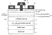
- the electron supply layer 23 has a structure that an i-In 0.52 Ga 0.48 As spacer layer 14, an Si- ⁇ doped layer 16 and an i-In 0.52 Ga 0.48 As barrier layer 18 are stacked in order as depicted in FIG. 3 .
- This configuration is referred to as first comparative example.
- the thickness of the i-In 0.52 Ga 0.48 As spacer layer 14 is approximately 3 nm and the thickness of the i-In 0.52 Ga 0.48 As barrier layer 18 is approximately 6 nm, and the thickness of the overall electron supply layer is equal to that of the embodiment described above.
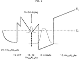
- a band discontinuity amount ⁇ E c of a conduction band E c between the electron supply layer 23 and the electron transit layer 13 does not increase very much.
- the Si- ⁇ doped layer 16 doped with an n-type impurity is provided on the electron supply layer 23 that functions as a barrier layer, the energy of the conduction band at the portion sometimes decreases, resulting in formation of a channel in which electrons are conducted also in the electron supply layer 23.
- a thin dotted line indicates a Fermi level E f and a thick dotted line indicates that the portion is Si- ⁇ -doped, and a waveform indicates an electron distribution.
- the channel in the electron supply layer 23 in which electrons are conducted namely, the ⁇ -doped portion, has an electron mobility and an electron speed lower than those in the electron transit layer 13. This is because the ⁇ -doped portion is an InAlAs layer in which the effective mass of electrons is heavy and that ionization impurity diffusion is great. Therefore, if a channel in which electrons are conducted is formed in the electron supply layer 23, namely, if parallel conduction occurs, then degradation of a characteristic is caused. For example, if parallel conduction occurs, then the overall delay time period is influenced not only by electrons in the electron transit layer 13 but also by electrons of the ⁇ -doped portion increases the value thereof, and this causes degradation of a characteristic of the cutoff frequency or the like. Accordingly, parallel conduction in the electron supply layer 23 that functions as a barrier layer is desired to be suppressed as far as possible without having an influence on some other delay time period or the like.
- the electron supply layer 23 so as to have a structure that, as depicted in FIG.
- an i-In x Al 1-x As (x ⁇ 0.52) spacer layer 14X for example, an i-In 0.4 Al 0.6 As spacer layer
- an Si- ⁇ doped layer 16 and an i-In x Al 1-x As (x ⁇ 0.52) barrier layer 18X are stacked in order, namely, such a conduction band structure as depicted in FIG. 6 to suppress parallel conduction. This is referred to as second comparative example.
- the i-In x Al 1-x As (x ⁇ 0.52) spacer layer 14X for example, an i-In 0.4 Al 0.6 As spacer layer
- the i-In x Al 1-x As (x ⁇ 0.52) barrier layer 18X for example, an i-In 0.4 Al 0.6 As barrier layer
- a thin broken line indicates a Fermi level E f and a thick broken line indicates that the portion is Si- ⁇ -doped, and a waveform in an InGaAs channel layer indicates an electron distribution.
- the energy of the conduction band E c of the electron supply layer 23 is increased entirely in this manner, then tunnel current and thermal current decrease and the contact resistance (ohmic contact resistance; contact resistance) of the source electrode 31 and drain electrode 32 increases and besides the delay time period of parasitic resistance increases, and this degrades a characteristic.
- a high-frequency characteristic value for example, a cutoff frequency f T , a maximum oscillation frequency f max or the like.
- the tunnel current is generated by passing of electrons in the electron supply layer 23 by a quantum-mechanical tunnel effect.
- the thermal current is generated by electrons that exceed a high barrier by thermal energy.
- the Al composition of InAlAs configuring the electron supply layer 23 is partially increased only in the proximity of the ⁇ doped portion as described above to increase the energy of the conduction band E c of the electron supply layer 23 partially only in the proximity of the ⁇ doped portion (refer to FIG. 2 ).
- the electron supply layer 23 has a structure that the i-In 0.52 Al 0.48 As spacer layer 14, an i-In x Al 1-x As (x ⁇ 0.52) layer 15 (for example, an i-In 0.4 Al 0.6 As layer), the Si- ⁇ doped layer 16, an i-In x Al 1-x As (x ⁇ 0.52) layer 17 (for example, an i-In 0.4 Al 0.6 As layer) and the i-In 0.52 Al 0.48 As barrier layer 18 are stacked in order.
- the energy of the conduction band E c does not decrease so much at the ⁇ doped portion and in the proximity of the ⁇ doped portion as that in the first comparative example (refer to FIG. 4 ) described above and parallel conduction in which the ⁇ doped portion functions as a channel in which electrons are conducted can be suppressed.
- the energy of the conduction band at the ⁇ doped portion and in the proximity of the ⁇ doped portion does not drop to a level equal to or lower than the Fermi energy E f , and parallel conduction in which the ⁇ doped portion functions as a channel in which electrons are conducted can be suppressed.
- the ratio of electrons existing in the electron supply layer 23 can be decreased to substantially 0 %.
- the energy of the conduction band E c of the entire electron supply layer does not increase so much as that of the second comparative example (refer to FIG. 6 ) described above, increase of the ohmic contact resistance of the source electrode 31 and the drain electrode 32 can be suppressed. Consequently, degradation of a characteristic arising from increase of the delay time period by increase of the ohmic contact resistance can be suppressed.
- the Al composition in the region to be doped with an n-type impurity is increased entirely to increase the energy of the conduction band E c in the overall region. Therefore, it is not sufficient to suppress degradation of a characteristic arising from increase of the delay time period by increase of the ohmic contact resistance described above.
- the energy of the conduction band at the portion doped with an n-type impurity and in the proximity of the portion decreases. Therefore, degradation of a characteristic arising from increase of the delay time period by increase of the ohmic contact resistance can be sufficiently suppressed.
- the ohmic contact resistance decreases and the delay time period by parasitic resistance reduces and the high-frequency characteristic value (for example, the cutoff frequency f T , maximum oscillation frequency f max or the like) increases.
- an n-type impurity is only doped partially into the portion at which the energy of the conduction band E c on the electron supply layer 23 has been increased.
- an impurity is not doped in the upper and lower portions sandwiching the ⁇ doped portion, namely, in the portions other than the ⁇ doped portion of the portion in which the energy of the conduction band E c has been increased. Therefore, it can be suppressed that an n-type impurity is dispersed from the ⁇ doped portion to the upper and lower portions (spacer layer 14 and barrier layer 18) sandwiching the portion at which the energy of the conduction band E c has been increased.
- the energy of the conduction band E c in the upper and lower portions (spacer layer 14 and barrier layer 18) sandwiching the portion at which the energy of the conduction band E c has been increased decreases and the energy of the conduction band E c at the boundary portion between the portion at which the energy of the conduction band E c has been increased and the upper and lower portions (spacer layer 14 and barrier layer 18) sandwiching the portion decreases, resulting in formation of a channel in which electrons are conducted at the boundary portion and occurrence of parallel conduction to degrade a characteristic.
- an n-type impurity may be dispersed from the region in which an n-type impurity is doped to the non-doped region and the energy of the conduction band E c in the non-doped region may decrease to decrease the energy of the conduction band E c at the boundary portion between the n-type impurity doped region and the non-doped region and form a channel in which electrons are conducted at the boundary portion, resulting in occurrence of parallel conduction to degrade a characteristic.
- the structure of the present embodiment that the ⁇ doped portion having a thickness equal to or smaller than a one-atom layer is sandwiched by the undoped portions and the structure of the conventional technology (first technology described above) that an n-type impurity is doped uniformly in the overall layer having a high Al composition and a thickness of approximately 1 nm can be distinguished from each other, for example, depending upon secondary ion mass spectrometry (SIMS).
- SIMS secondary ion mass spectrometry
- MBE molecular beam epitaxy
- the buffer layer 11 has a thickness set to approximately 1000 nm.
- the i-In 0.52 Al 0.48 As layer 12 has a thickness set to approximately 200 nm.
- the i-InGaAs electron transit layer 13 has a thickness set to approximately 10 nm.
- the i-In 0.52 Al 0.48 As spacer layer 14 has a thickness set to approximately 2 nm.
- the i-In 0.4 Al 0.6 As layer 15 has a thickness set to approximately 1 nm.
- the Si- ⁇ doped layer 16 has a ⁇ doping amount of Si set to approximately 1 ⁇ 10 13 cm -2 .
- the i-In 0.4 Al 0.6 As layer 17 has a thickness set to approximately 1 nm.
- the i-In 0.52 Ga 0.48 As barrier layer 18 has a thickness set to approximately 5 nm. Further, the i-InP etching stopping layer 19 has a thickness set to approximately 3 nm. Further, the n-In 0.53 Ga 0.47 As cap layer 20 has a thickness set to approximately 20 nm and an Si doping amount set to approximately 2 ⁇ 10 19 cm -3 .
- a source electrode 31 and a drain electrode 32 individually having a three-layer structure, for example, of Ti/Pt/Au are formed as depicted in FIG. 7(B) . Consequently, the source electrode 31 and the drain electrode 32 are formed on the n-In 0.53 Ga 0.47 As cap layer 20.
- an SiO 2 film 21 is formed on the n-In 0.53 Ga 0.47 As cap layer 20 between the source electrode 31 and the drain electrode 32 as depicted in FIG. 7 (C) , for example, by a plasma CVD (Chemical Vapor Deposition) method.
- the SiO 2 film 21 has a thickness of approximately 20 nm.
- a T-shaped gate electrode 33 is formed as depicted in FIGS. 8(A) to 9(C) .
- resist films 41 to 43 having a three-layer structure are formed first as depicted in FIG. 8(A) .
- a ZEP resist by Zeon Corporation
- a PMGI Poly-dimethylglutarimide resist and the ZEP resist are applied in order to form the resist films having a three-layer structure that a ZEP resist film 41, a PMGI resist film 42 and a ZEP resist film 43 are stacked in order.
- a region in which a head portion of the T-shaped gate electrode 33 is to be formed is exposed to form an opening on the ZEP resist film 43 and the PMGI resist film 42 as depicted in FIG. 8(B) .
- a region in which a foot portion of the T-shaped gate electrode 33 is to be formed is exposed to form an opening in accordance with a desired gate length on the ZEP resist film 41 of the lowest layer as depicted in FIG. 8(C) .
- an opening is formed in the SiO 2 film 21 as depicted in FIG. 9(A) , for example, by reactive ion etching in which CF 4 is used as etching gas using the ZEP resist film 41 of the lowest layer having the opening formed in accordance with the gate length as a mask.
- wet etching is performed, for example, using mixture solution of citric acid (C 6 H B O 7 ) and hydrogen peroxide solution (H 2 O 2 ) as etching liquid to form a recess as depicted in FIG. 9(B) .
- T-shaped gate electrode 33 having a three-layer structure of, for example, Ti/Pt/Au as depicted in FIG. 9(C) . Consequently, the T-shaped gate electrode 33 is formed on the i-InP etching stopping layer 19.
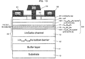
- the Al composition of the electron supply layer 23 is set to increase stepwise only in the proximity of (around) the ⁇ doped portion
- the AI composition is not limited to this.
- InAlAs layers having a gradient composition may be provided such that the Al composition gradually increases toward the portion at which the Al composition in the proximity of the ⁇ doped portion is set high.
- Such a gradient composition InAlAs layer as described above can be formed by gradually increasing the Al composition, for example, from In 0.52 Al 0.48 As that lattice-matches with the In 0.53 Al 0.47 As electron transit layer 13 to In 0.4 Al 0.6 As and performing ⁇ doping while maintaining the composition and then further maintaining the composition, whereafter the Al composition is gradually decreased to In 0.52 Al 0.48 As.
- the Al composition is gradually decreased to In 0.52 Al 0.48 As.
- the conduction band structure becomes such as depicted in FIG. 11 . It is to be noted that, in FIG.
- a thin broken line indicates a Fermi level E f and a thick broken line indicates that the portion is Si- ⁇ -doped, and a waveform in an InGaAs channel layer indicates an electron distribution.
- the energy of the conduction band E c does not decrease so much at the ⁇ doped portion and in the proximity of the ⁇ doped portion as that in the first comparative example (refer to FIG. 4 ) described hereinabove and parallel conduction in which the ⁇ doped portion functions as a channel in which electrons are conducted can be suppressed. Therefore, degradation of a characteristic by parallel conduction can be suppressed.
- the ohmic contact resistance increases exceeding that of the embodiment described above, the ohmic contact resistance does not increase so much as that in the second comparative example (refer to FIG. 6 ) described hereinabove. Therefore, degradation of a characteristic arising from increase of the delay time period by increase of the ohmic contact resistance can be suppressed. Further, similarly as in the embodiment (refer to FIG. 2 ) described hereinabove, the energy of the conduction band E c of the electron supply layer 23 is only partially increased.
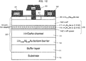
- the electron supply layer 23 has a structure that the InAlAs spacer layer 14, InAlAs layer 15, Si- ⁇ doped layer 16, InAlAs layer 17 and InAlAs barrier layer 18 are stacked in order, the structure of the electron supply layer 23 is not limited to this.
- the electron supply layer 23 may be configured so as to have a structure that an InP spacer layer 14Z (second portion), an InAlAs layer 15 (first portion; undoped portion), an Si- ⁇ doped layer 16 (first portion; doped portion), an InAlAs layer 17 (first portion; undopedportion) and an InP barrier layer 18Z (second portion) are stacked in order.
- the InP barrier layer 18Z functions also as an etching stopping layer.
- the first portion and the second portion include semiconductor materials different from each other.
- the electron supply layer 23 may be configured so as to have a structure that an i-InP spacer layer 14Z, an i-In 0.52 Al 0.48 As layer 15, an Si- ⁇ doped layer 16, an i-In 0.52 Al 0.48 As layer 17 and an i-InP barrier layer 18Z are stacked in order.
- the InAlAs layers 15 and 17 here namely, InAlAs layers 15 and 17 for which ⁇ doping is to be performed
- the configuration of the InAlAs layers 15 and 17 is not limited to this.
- the Al composition may be increased (for example, formed as i-In 0.4 Al 0.6 As layers) and the energy (potential) of the conduction band of the ⁇ doped portion and in the proximity of the portion may be increased. Therefore, the InAlAs layers 15 and 17 that sandwich the Si- ⁇ doped layer 16 (namely, the InAlAs layers 15 and 17 for which ⁇ doping is to be performed) may be i-In x Al 1-x As (x ⁇ 0.52) layers. Where such a configuration as just described is applied, the conduction band structure becomes such as depicted in FIG. 13 . It is to be noted that, in FIG.
- a thin broken line indicates a Fermi level E f and a thick broken line indicates that the portion is Si- ⁇ -doped, and a waveform in an InGaAs channel layer indicates an electron distribution.
- This is referred to as second modification. Even if the semiconductor device according to the second modification configured in such a manner as described above is applied, an effect similar to that of the embodiment described above can be obtained.
- the material system is not limited to this.
- a semiconductor stacked structure 22A may be provided in which a buffer layer 11A, an AlGaAs lower barrier layer 12A, a GaAs electron transit layer 13A, an AlGaAs electron supply layer 23A and a GaAs cap layer 20A are stacked in order on a GaAs substrate 10A.
- a semiconductor stacked structure 22A may be provided in which a buffer layer 11A, an i-Al x Ga 1-x As lower barrier layer 12A, an i-GaAs electron transit layer 13A, an i-AlGaAs electron supply layer 23A and an n-GaAs cap layer 20A are stacked in order on the GaAs substrate 10A.
- the i-AlGaAs electron supply layer 23A may be configured so as to have a structure that an i-Al x Ga 1-x As spacer layer 14A (second portion), an i-Al y Ga 1-y As (x ⁇ y) layer 15A (first portion; undoped portion), an Si- ⁇ doped layer 16A (first portion; doped portion), an i-Al y Ga 1-y As (x ⁇ y) layer 17A (first portion; undoped portion) and an i-Al x Ga 1-x As barrier layer 18A (second portion) are stacked in order.
- the Al composition of AlGaAs configuring the electron supply layer 23A may be partially increased only in the proximity of the ⁇ doped portion such that the energy of the conduction band E c of the electron supply layer 23A is partially increased only in the proximity of the ⁇ doped portion.
- the conduction band structure becomes such as depicted in FIG. 15 . It is to be noted that, in FIG.
- a thin broken line indicates a Fermi level E f and a thick broken line indicates that the portion is Si- ⁇ -doped, and a waveform in an InGaAs channel layer indicates an electron distribution.
- the electron transit layer 13 may be configured as an InGaAs layer such as, for example, an In 0.15 Ga 0.85 As layer by adding some InAs thereto.
- the cap layer 20A may be configured as a GaAs layer (n-type GaAs layer), an InGaAs layer (n-type InGaAs layer) or a layer in which an InGaAs layer and a GaAs layer are stacked (layer in which an n-type InGaAs layer and an n-type GaAs layer are stacked).
- This is referred to as AlGaAs/InGaAs-based HEMT.
- This is referred to as third modification. Also with the third modification configured in such a manner as just described, an effect similar to that achieved by the embodiment described above can be achieved.
- a gradient composition AlGaAs layer may be used for the barrier layer 18A and the spacer layer 14A configuring the electron supply layer 23A of the third modification as in the first modification described above.
- the first and second portions contain Al.
- the first portion has an Al composition higher than that of the second portion and has energy of the conduction band E c higher than that of the second portion.
- the first portion and the second portion include semiconductor materials same as each other but include compositions different from each other.
- the first portion has a doped portion doped with an n-type impurity and undoped portions that sandwich the doped portion and are not doped with an impurity.
- the doped portion is a portion at which an n-type impurity is planar-doped, and the n-type impurity is Si. Further, the second portion is not doped with an impurity. It is to be noted that an AlGaAs/GaAs-based chemical semiconductor or an AlGaAs/InGaAs-based chemical compound is referred to as III-V group chemical compound.
- a semiconductor stacked structure 22B may be provided in which a buffer layer 11B, a GaN electron transit layer 13B and an AlGaN electron supply layer 23B are stacked in order on an SiC substrate 10B.
- a semiconductor stacked structure 22B may be provided in which a buffer layer 11B, an i-GaN electron transit layer 13B and an i-AlGaN electron supply layer 23B are stacked in order on an SiC substrate 10B.
- the i-AlGaN electron supply layer 23B may be configured so as to have a structure that an i-Al x Ga 1-x N spacer layer 14B (second portion), an i-Al y Ga 1-y N (x ⁇ y) layer 15B (first portion; undoped portion), an Si- ⁇ doped layer 16B (first portion; doped portion), an i-Al y Ga 1-y N (x ⁇ y) layer 17B (first portion; undoped portion) and an i-Al x Ga 1-x N barrier layer 18B (second portion) are stacked in order.
- the Al composition (AlN composition) of AlGaN configuring the electron supply layer 23B is partially increased only in the proximity of the ⁇ doped portion such that the energy of the conduction band E c of the electron supply layer 23B is partially increased only in the proximity of the ⁇ doped portion.
- the conduction band structure becomes such as depicted in FIG. 17 . It is to be noted that, in FIG.
- a thin broken line indicates a Fermi level E f and a thick broken line indicates that the portion is Si- ⁇ -doped, and a waveform in a GaN channel layer indicates an electron distribution.
- AlGaN is used as a semiconductor material configuring the layers of the electron supply layer 23B
- the semiconductor material is not limited to this and, for example, an InAlN layer may be used. This is referred to as InAlN/GaN-based HEMT.
- also confining of electrons can be improved by providing, for example, an i-Al z Ga 1-z N lower barrier layer at the lower side of the electron transit layer 13B. In this case, z may be approximately 0.05 to approximately 0.10.
- an n-type GaN cap layer may be provided on the electron supply layer 23B.
- the ohmic resistance can be decreased by providing the Si- ⁇ doped layer 16B in the AlGaN/GaN-based HEMT or an InAlN/GaN-based HEMT.
- This is referred to as fourth modification.
- a gradient composition AlGaN layer may be used for the barrier layer 18B and the spacer layer 14B configuring the electron supply layer 23B of the fourth modification as in the first modification described above.
- the first and second portions contain Al.
- the first portion has an Al composition higher than that of the second portion and has energy of the conduction band higher than that of the second portion.
- the first portion and the second portion include semiconductor materials same as each other but include compositions different from each other.
- the first portion has a doped portion doped with an n-type impurity and undoped portions that sandwich the doped portion and are not doped with an impurity.
- the doped portion is a portion at which an n-type impurity is planar-doped, and the n-type impurity is Si.
- the second portion is not doped with an impurity.
- an AlGaN/GaN-based chemical semiconductor or an InAlN/GaN-based chemical compound is referred to as III-V group chemical compound. It is to be noted that also a sapphire substrate or an Si (111) substrate can be used as the substrate 10B for use for a nitride semiconductor.
Landscapes
- Junction Field-Effect Transistors (AREA)
Abstract
Description
- The present invention relates to a semiconductor device.
- Conventionally, a semiconductor device is available which includes a semiconductor stacked structure including an electron transit layer and an electron supply layer provided over a substrate.
- In such a semiconductor device as just described, since an n-type impurity is doped in the electron supply layer that functions also as a barrier layer, energy of a conduction band sometimes drops at the portion at which the n-type impurity is doped and a channel by which electrons are conducted is formed also in the electron supply layer. In particular, a situation in which electrons are conducted in the electron supply layer other than the electron transit layer, namely, so-called parallel conduction, sometimes occurs.
- Since a channel in the electron supply layer by which electrons are conducted has an electron mobility and an electronic speed lower than those in the electron transit layer, if a channel by which electrons are conducted is formed in the electron supply layer, namely, if the parallel conduction occurs, then degradation in characteristic is caused.
- Thus, a technology is available that, by setting a composition of Al in a region in which an n-type impurity is to be doped higher than a composition of Al in a non-doped region, for example, in an AlGaN barrier layer, energy of the conduction band of the region in which the n-type impurity is to be doped is increased and decrease of the energy of the conduction band arising from doping with the n-type impurity is compensated for. This is referred to as first technology.
- It is to be noted that also a configuration is available that an InAlAs layer having a high composition of Al is provided on the opposite sides across an InAlAs electron supply layer in which the n-type impurity is doped entirely.
-
- PTL 1:
Japanese Laid-Open Patent Application No. 2005-302861 - PTL 2:
Japanese Laid-Open Patent Application No. 2001-177089 - Incidentally, it seems a possible idea to increase, for example, energy of the conduction band of the overall electron supply layer in order to suppress the parallel conduction described above. However, if the energy of the conduction band of the overall electron supply layer is increased, then tunnel current and thermal current of electrons decrease and contact resistance (ohmic contact resistance) of the source electrode and the drain electrode increases and besides the delay time period by parasitic resistance increases. Consequently, a characteristic is degraded.
- Further, in the first technology described above, in order to compensate for decrease of energy of the conduction band caused by doping of an n-type impurity, the composition of Al of the overall region in which the n-type impurity is to be doped is increased to increase the energy of the conduction band of the overall region. However, the countermeasure just described is insufficient to suppress degradation in characteristic arising from increase of the delay time period by increase of the ohmic contact resistance described above. Further, there is the possibility that the n-type impurity may be dispersed from the region in which the n-type impurity is doped to the non-doped region and the energy of the conduction band in a boundary portion between the n-type impurity doped region and the non-doped region may decrease and then a channel by which electrons are conducted may be formed at the boundary portion to cause parallel conduction to degrade a characteristic.
- Therefore, it is desirable to suppress parallel conduction and suppress degradation of a characteristic by the parallel conduction while degradation of a characteristic caused by increase of a delay time period by increase of ohmic contact resistance is sufficiently suppressed.
- The present semiconductor device includes a semiconductor stacked structure including at least an electron transit layer and an electron supply layer over a substrate, wherein the electron supply layer includes a first portion and second portions sandwiching the first portion, and the first portion has a higher energy of a conduction band than that of the second portion, and includes a doped portion doped with an n-type impurity and undoped portions that sandwich the doped portion and are not doped with an impurity.
- Accordingly, with the present semiconductor device, there is an advantage that parallel conduction is suppressed while degradation of a characteristic caused by increase of the delay time period by increase of the ohmic contact resistance is sufficiently suppressed and degradation of a characteristic arising from the parallel conduction can be suppressed.
-
- [
FIG. 1] FIG. 1 is a schematic sectional view depicting a configuration of a semiconductor device (InAlAs/InGaAs-based HEMT; InP-based HEMT) of a present embodiment. - [
FIG. 2] FIG. 2 is a schematic view depicting a conduction band structure of the semiconductor device (InAlAs/InGaAs-based HEMT; InP-based HEMT) of the present embodiment. - [
FIG. 3] FIG. 3 is a schematic sectional view depicting a configuration of a semiconductor device (InAlAs/InGaAs-based HEMT; InP-based HEMT) of a first comparative example. - [
FIG. 4] FIG. 4 is a schematic view depicting a conduction band structure of the semiconductor device (InAlAs/InGaAs-based HEMT; InP-based HEMT) of the first comparative example. - [
FIG. 5] FIG. 5 is a schematic sectional view depicting a configuration of a semiconductor device (InAlAs/InGaAs-based HEMT; InP-based HEMT) of a second comparative example. - [
FIG. 6] FIG. 6 is a schematic view depicting a conduction band structure of the semiconductor device (InAlAs/InGaAs-based HEMT; InP-based HEMT) of the second comparative example. - [
FIG. 7] FIGS. 7(A) to 7(C) are schematic sectional views illustrating a fabrication method for the semiconductor device (InAlAs/InGaAs-based HEMT; InP-based HEMT) of the present embodiment. - [
FIG. 8] FIGS. 8(A) to 8(C) are schematic sectional views illustrating a fabrication method for the semiconductor device (InAlAs/InGaAs-based HEMT; InP-based HEMT) of the present embodiment. - [
FIG. 9] FIGS. 9(A) to 9(C) are schematic sectional views illustrating a fabrication method for the semiconductor device (InAlAs/InGaAs-based HEMT; InP-based HEMT) of the present embodiment. - [
FIG. 10] FIG. 10 is a schematic sectional view depicting a configuration of a semiconductor device (InAlAs/InGaAs-based HEMT; InP-based HEMT) of a first modification to the present embodiment. - [
FIG. 11] FIG. 11 is a schematic view depicting a conduction band structure of the semiconductor device (InAlAs/InGaAs-based HEMT; InP-based HEMT) of the first modification to the present embodiment. - [
FIG. 12] FIG. 12 is a schematic sectional view depicting a configuration of a semiconductor device (InP-based HEMT) of a second modification to the present embodiment. - [
FIG. 13] FIG. 13 is a schematic view depicting a conduction band structure of the semiconductor device (InP-based HEMT) of the second modification to the present embodiment. - [
FIG. 14] FIG. 14 is a schematic sectional view depicting a configuration of a semiconductor device (AlGaAs/GaAs-based HEMT) of a third modification to the present embodiment. - [
FIG. 15] FIG. 15 is a schematic view depicting a conduction band structure of the semiconductor device (AlGaAs/GaAs-based HEMT) of the third modification to the present embodiment. - [
FIG. 16] FIG. 16 is a schematic sectional view depicting a configuration of a semiconductor device (AlGaN/GaN-based HEMT) of a fourth modification to the present embodiment. - [
FIG. 17] FIG. 17 is a schematic view depicting a conduction band structure of the semiconductor device (AlGaN/GaN-based HEMT) of the fourth modification to the present embodiment. - In the following, a semiconductor device according to an embodiment of the present invention is described with reference to
FIGS. 1 to 9 of the drawings. - The semiconductor device according to the present embodiment includes an InP-based high electron mobility transistor (HEMT) that is one of ultra-high-speed transistors used, for example, for communication. In particular, the present semiconductor device includes an InP-based HEMT having a semiconductor stacked structure in which an InAlAs/InGaAs-based compound semiconductor is used, for example, on an InP substrate. The InP-based HEMT is a transistor capable of operating in a region of, for example, a millimeter wave (approximately 30 to approximately 300 GHz) or a submillimeter wave (approximately 300 GHz to approximately 3 THz). It is to be noted that the InAlAs/InGaAs-based compound semiconductor is referred to sometimes as III-V group compound semiconductor. Further, the InP-based HEMT is referred to sometimes as InAlAs/InGaAs-based HEMT.
- As depicted in
FIG. 1 , the present InP-based HEMT includes asubstrate 10, a semiconductor stackedstructure 22 provided on thesubstrate 10, and agate electrode 33, asource electrode 31 and adrain electrode 32 provided on the semiconductor stackedstructure 22. - In the present embodiment, the
substrate 10 is a semi-insulating InP substrate (semiconductor substrate). It is to be noted that, as thesubstrate 10, also a GaAs substrate or an Si substrate can be used. - The semiconductor stacked
structure 22 is a semiconductor stacked structure including an electron transit layer (channel layer) 13 and an electron supply layer (barrier layer) 23. Here, the semiconductor stackedstructure 22 has a structure that abuffer layer 11, alower barrier layer 12, theelectron transit layer 13, theelectron supply layer 23, anetching stopping layer 19 and acap layer 20 are stacked in order. - In the present embodiment, the
buffer layer 11 has a thickness of, for example, approximately 1000 nm. It is to be noted that a material to be used for thebuffer layer 11 is different depending upon thesubstrate 10. - The
lower barrier layer 12 is an InAlAs layer. Here, thelower barrier layer 12 is an undoped InAlAs layer. For example, thelower barrier layer 12 is an i-In0.52Al0.48As layer and has a thickness of approximately 200 nm. - The
electron transit layer 13 is an InGaAs layer. In particular, theelectron transit layer 13 includes InGaAs. Here, theelectron transit layer 13 is an undoped InGaAs layer. For example, theelectron transit layer 13 is an i-In0.53Ga0.47As layer and has a thickness of approximately 10 nm. It is to be noted that an In0.53Ga0.47As layer that lattice-matches with InP may not be used as theelectron transit layer 13, and the InAs composition may be increased so as to be higher than 0.53 as in an In0.7Ga0.3As layer to which compression distortion is applied or the like. - The
electron supply layer 23 has a structure that anInAlAs spacer layer 14, anInAlAs layer 15, an Si-δ dopedlayer 16, anInAlAs layer 17 and anInAlAs barrier layer 18 are stacked in order. Here, theelectron supply layer 23 has a structure that an undopedInAlAs spacer layer 14, an undopedInAlAs layer 15, an Si-δ dopedlayer 16 δ-doped with Si that is an n-type impurity, an undopedInAlAs layer 17 and an undopedInAlAs barrier layer 18 are stacked in order. For example, theelectron supply layer 23 has a structure that an i-In0.52Ga0.48Asspacer layer 14 having a thickness of approximately 2 nm, an i-In0.4Ga0.6Aslayer 15 having a thickness of approximately 1 nm, an Si-δ dopedlayer 16 in which the δ doping amount of Si is approximately 1 × 1013 cm-2, an i-In0.4Ga0.6Aslayer 17 having a thickness of approximately 1 nm and an i-In0.52Ga0.48Asbarrier layer 18 having a thickness of approximately 5 nm are stacked in order. - It is to be noted that, while the InAlAs layers 15 and 17 that sandwich the Si-δ doped
layer 16, namely, InAlAs layers for which δ doping is to be performed, are i-In0.4Ga0.6As layers here, the InAlAs layers are not limited to this, and i-InxAl1-xAs (x < 0.52) layers may be used. In particular, the InAlAs layers 15 and 17 may formed so as to have a higher composition of Al (AlAs composition) than that of theInAlAs spacer layer 14 and theInAlAs barrier layer 18 that sandwich the InAlAs layers 15 and 17. - Further, the Si-o doped
layer 16 is configured by forming an element (here, Si) to be used as an n-type impurity as a very thin film having a thickness equal to or thinner than a one-atom layer without supplying, upon crystal growth of InAlAs, a III group element and a V group element. The Si-δ dopedlayer 16 and the InAlAs layers 15 and 17 sandwiching the Si-δ dopedlayer 16 can be entirely considered as a layer in which an element (here, Si) to be used as an n-type impurity is planar-doped between the InAlAs layers. The Si-δ dopedlayer 16 is referred to sometimes as n-type impurity doped layer, n-type impurity planar-doped layer, n-type impurity layer or n-type impurity atom layer. In this manner, an n-type impurity is not doped uniformly but is σ-doped, namely, planar-doped, into a region in which the energy of the conduction band is increased by increasing the Al composition of the InAlAs configuring theelectron supply layer 23. By the δ doping, the n-type impurity is doped partially into the region in which the energy of the conduction band is increased by increasing the Al composition of InAlAs. This is effective to form, when a gate length Lg is to be refined in order to achieve increase of the speed of the HEMT, the electron supply layer between the gate electrode and the electron transit layer as thin as possible in accordance with the refinement of the gate length Lg from a view point of scaling. - Further, the
InAlAs layer 15, Si-δ dopedlayer 16 andInAlAs layer 17 are referred to sometimes as first portion. Further, theInAlAs spacer layer 14 and theInAlAs barrier layer 18 are referred to as second portion. In this case, theelectron supply layer 23 has the first portion and the second portions that sandwich the first portion, and the first and second portions individually contain InAlAs, namely, the first and second portions individually contain Al, and besides the first portion has a composition of Al higher than that of the second portions. Therefore, the first portion is higher in energy of the conduction band than the second portion. In this manner, the first portion and the second portions that configure theelectron supply layer 23 contain the same semiconductor material but have compositions different from each other. Further, since the Si-δ dopedlayer 16 is a portion δ-doped with Si as an n-type impurity, the Si-δ dopedlayer 16 is referred to sometimes as doped portion doped with an n-type impurity or as doped portion planar-doped with an n-type impurity. Further, since the InAlAs layers 15 and 17 sandwiching the Si-δ dopedlayer 16, namely, the InAlAs layers to which δ doping is to be performed, are undoped InAlAs layers, the InAlAs layers 15 and 17 are referred to sometimes as undoped portion not doped with an impurity. In this case, the first portion includes a doped portion doped with an n-type impurity and undoped portions that sandwich the doped portion and are not doped with an impurity. Further, since theInAlAs spacer layer 14 and theInAlAs barrier layer 18 are undoped InAlAs layers, the second portions are not doped with an impurity. - In this manner, in the present embodiment, InAlAs is used for the
electron supply layer 23 and the Al composition of an intermediate portion (inner side portion) sandwiched by the upper side portion and the lower side portion (outer side portions) is increased to increase the energy of the conduction band of the intermediate portion. In particular, the portion at which the energy of the conduction band is increased by increasing the Al composition is sandwiched by the portions that have an Al composition and energy of the conduction band lower than those of the portion to be sandwiched. Further, planar doping (δ doping) of an n-type impurity is performed for the central position in the thicknesswise direction of the intermediate portion having high energy of the conduction band. In particular, the portion planar-doped with the n-type impurity is sandwiched by the portions that have high energy of the conduction band and are not doped with an impurity. In this manner, the region in which the energy of the conduction band is high is provided partially within theelectron supply layer 23 and an n-type impurity is doped partially in the region in which the energy of the conduction band is high. Consequently, the portion doped with the n-type impurity is sandwiched by the portions that have high energy of the conduction band and are not doped with an impurity, and the portions that have high energy of the conduction band and are not doped with an impurity are sandwiched by the portions that have energy of the conduction band lower than that of the portions and are not doped with an impurity. - It is to be noted that, while InAlAs is used as a semiconductor material configuring the layers of the
electron supply layer 23 here, the semiconductor material is not limited to this and, for example, InAlAsSb may be used. - The
etching stopping layer 19 is an InP layer and is an etching stopping layer for thecap layer 20. Here, theetching stopping layer 19 is an undoped InP layer, namely, an i-InP layer and has a thickness of approximately 3 nm. It is to be noted theetching stopping layer 19 has also a function as a protective layer for preventing oxidation of an InAlAs electron supply layer. - The
cap layer 20 is an InGaAs layer. Here, thecap layer 20 is an n-InGaAs layer in which Si is doped to provide an n-type conductivity. For example, thecap layer 20 is an n-In0.53Ga0.47As layer, and has a thickness of approximately 20 nm and has an Si doping amount of approximately 2 × 1019 cm-3. It is to be noted that thecap layer 20 may be configured as a cap layer having a two-layer structure formed by stacking an n-In0.70Ga0.30As layer on an n-In0.53Ga0.47As layer. Further, thecap layer 20 may be configured as a cap layer having a two-layer structure formed by stacking an n-type InGaAs layer and an n-type InAlAs layer. - The conduction band structure of the semiconductor stacked
structure 22 configured in such a manner as described above is depicted inFIG. 2 . It is to be noted that, inFIG. 2 , a thin dotted line indicates a Fermi level Ef and a thick dotted line indicates that the portion is Si-δ-doped, and a waveform in an InGaAs channel layer indicates an electron distribution. - It is to be noted that the semiconductor stacked
structure 22 may include at least theelectron transit layer 13 and theelectron supply layer 23 over thesubstrate 10 and may include a different stacked structure. Further, the semiconductor stackedstructure 22 is referred to sometimes as hetero structure semiconductor layer. - The
gate electrode 33,source electrode 31 anddrain electrode 32 are provided on the semiconductor stackedstructure 22 configured in such a manner as described above, and the surface of the semiconductor stackedstructure 22 is covered with an SiO2 film (insulating film) 21. - Here, the
source electrode 31 and thedrain electrode 32 configured, for example, fromTi/Pt/Au are provided on the n-InGaAs cap layer 20. Further, thegate electrode 33 configured, for example, from Ti/Pt/Au is provided on the i-InP layer 19. - Incidentally, the reason why the
electron supply layer 23 in the present embodiment is configured as described above is described below. - For example, the
electron supply layer 23 has a structure that an i-In0.52Ga0.48Asspacer layer 14, an Si-δ dopedlayer 16 and an i-In0.52Ga0.48Asbarrier layer 18 are stacked in order as depicted inFIG. 3 . This configuration is referred to as first comparative example. It is to be noted that, in this case, the thickness of the i-In0.52Ga0.48Asspacer layer 14 is approximately 3 nm and the thickness of the i-In0.52Ga0.48Asbarrier layer 18 is approximately 6 nm, and the thickness of the overall electron supply layer is equal to that of the embodiment described above. - In this case, for example, as depicted in
FIG. 4 in which a conduction band structure is depicted, a band discontinuity amount ΔEc of a conduction band Ec between theelectron supply layer 23 and theelectron transit layer 13 does not increase very much. Further, since the Si-δ dopedlayer 16 doped with an n-type impurity is provided on theelectron supply layer 23 that functions as a barrier layer, the energy of the conduction band at the portion sometimes decreases, resulting in formation of a channel in which electrons are conducted also in theelectron supply layer 23. In particular, the energy of the conduction band Ec of the δ doped portion in theelectron supply layer 23, namely, of the Si-δ dopedlayer 16 sandwiched by the i-In0.52Ga0.48Asspacer layer 14 and the i-In0.52Ga0.48Asbarrier layer 18 configuring theelectron supply layer 23, decreases sharply and the energy of the conduction band Ec of the δ doped portion becomes equal to or lower than the Fermi energy Ef. Then, a channel in which electrons are conducted is formed also at the δ doped portion, and electrons are sometimes conducted also in theelectron supply layer 23 other than theelectron transit layer 13, namely, so-called parallel conduction sometimes occurs. It is to be noted that, inFIG. 4 , a thin dotted line indicates a Fermi level Ef and a thick dotted line indicates that the portion is Si-δ-doped, and a waveform indicates an electron distribution. - The channel in the
electron supply layer 23 in which electrons are conducted, namely, the δ-doped portion, has an electron mobility and an electron speed lower than those in theelectron transit layer 13. This is because the δ-doped portion is an InAlAs layer in which the effective mass of electrons is heavy and that ionization impurity diffusion is great. Therefore, if a channel in which electrons are conducted is formed in theelectron supply layer 23, namely, if parallel conduction occurs, then degradation of a characteristic is caused. For example, if parallel conduction occurs, then the overall delay time period is influenced not only by electrons in theelectron transit layer 13 but also by electrons of the δ-doped portion increases the value thereof, and this causes degradation of a characteristic of the cutoff frequency or the like. Accordingly, parallel conduction in theelectron supply layer 23 that functions as a barrier layer is desired to be suppressed as far as possible without having an influence on some other delay time period or the like. - It seems a possible idea to generally increase, in order to suppress such parallel conduction as described above, the Al composition of InAlAs configuring the
electron supply layer 23 to increase the energy of the conduction band Ec of the entire electron supply layer, namely, to increase the band discontinuity amount of the conduction band Ec of theelectron supply layer 23 and theelectron transit layer 13. For example, it seems a possible idea to configure theelectron supply layer 23 so as to have a structure that, as depicted inFIG. 5 , an i-InxAl1-xAs (x < 0.52) spacer layer 14X (for example, an i-In0.4Al0.6As spacer layer), an Si-δ dopedlayer 16 and an i-InxAl1-xAs (x < 0.52)barrier layer 18X (for example, an i-In0.4Al0.6As barrier layer) are stacked in order, namely, such a conduction band structure as depicted inFIG. 6 to suppress parallel conduction. This is referred to as second comparative example. It is to be noted that the i-InxAl1-xAs (x < 0.52) spacer layer 14X (for example, an i-In0.4Al0.6As spacer layer) and the i-InxAl1-xAs (x < 0.52)barrier layer 18X (for example, an i-In0.4Al0.6As barrier layer) are same as those in the case of the first comparative example described above. It is to be noted that, inFIG. 6 , a thin broken line indicates a Fermi level Ef and a thick broken line indicates that the portion is Si-δ-doped, and a waveform in an InGaAs channel layer indicates an electron distribution. - However, if the energy of the conduction band Ec of the
electron supply layer 23 is increased entirely in this manner, then tunnel current and thermal current decrease and the contact resistance (ohmic contact resistance; contact resistance) of thesource electrode 31 anddrain electrode 32 increases and besides the delay time period of parasitic resistance increases, and this degrades a characteristic. For example, if the ohmic contact resistance increases and the delay time period by parasitic resistance increases, then a high-frequency characteristic value (for example, a cutoff frequency fT, a maximum oscillation frequency fmax or the like) decreases. It is to be noted that the tunnel current is generated by passing of electrons in theelectron supply layer 23 by a quantum-mechanical tunnel effect. Further, the thermal current is generated by electrons that exceed a high barrier by thermal energy. - Therefore, in the present embodiment, the Al composition of InAlAs configuring the
electron supply layer 23 is partially increased only in the proximity of the δ doped portion as described above to increase the energy of the conduction band Ec of theelectron supply layer 23 partially only in the proximity of the δ doped portion (refer toFIG. 2 ). Here, an InxAl1-xAs layer (x < 0.52; for example, x = approximately 0.4) is provided over and under the δ doped portion in the i-In0.52Al0.48As layer configuring theelectron supply layer 23 so that the Al composition (AlAs composition) in theelectron supply layer 23 is increased stepwise only in the proximity of the δ doped portion. In this case, theelectron supply layer 23 has a structure that the i-In0.52Al0.48Asspacer layer 14, an i-InxAl1-xAs (x < 0.52) layer 15 (for example, an i-In0.4Al0.6As layer), the Si-δ dopedlayer 16, an i-InxAl1-xAs (x < 0.52) layer 17 (for example, an i-In0.4Al0.6As layer) and the i-In0.52Al0.48Asbarrier layer 18 are stacked in order. - Consequently, as indicated by the conduction band structure of
FIG. 2 , the energy of the conduction band Ec does not decrease so much at the δ doped portion and in the proximity of the δ doped portion as that in the first comparative example (refer toFIG. 4 ) described above and parallel conduction in which the δ doped portion functions as a channel in which electrons are conducted can be suppressed. In other words, the energy of the conduction band at the δ doped portion and in the proximity of the δ doped portion does not drop to a level equal to or lower than the Fermi energy Ef, and parallel conduction in which the δ doped portion functions as a channel in which electrons are conducted can be suppressed. Therefore, degradation of a characteristic by parallel conduction can be suppressed. For example, as regards the electron distribution, while electrons of approximately 10 % can exist in theelectron supply layer 23 in the first comparative example (refer toFIG. 4 ) described above, in the present embodiment, the ratio of electrons existing in theelectron supply layer 23 can be decreased to substantially 0 %. Further, since also the energy of the conduction band Ec of the entire electron supply layer does not increase so much as that of the second comparative example (refer toFIG. 6 ) described above, increase of the ohmic contact resistance of thesource electrode 31 and thedrain electrode 32 can be suppressed. Consequently, degradation of a characteristic arising from increase of the delay time period by increase of the ohmic contact resistance can be suppressed. - Furthermore, since only the energy of the conduction band Ec of the
electron supply layer 23 is increased partially, degradation of a characteristic arising from increase of the delay time period by increase of the ohmic contact resistance can be sufficiently suppressed. In contrast, in the conventional technology (first technology described above), in order to compensate for decrease of energy of the conduction band Ec caused by doping of an n-type impurity, the Al composition in the region to be doped with an n-type impurity is increased entirely to increase the energy of the conduction band Ec in the overall region. Therefore, it is not sufficient to suppress degradation of a characteristic arising from increase of the delay time period by increase of the ohmic contact resistance described above. In this manner, in comparison with the conventional technology (first technology described), by applying the configuration described above as in the present embodiment, the energy of the conduction band at the portion doped with an n-type impurity and in the proximity of the portion decreases. Therefore, degradation of a characteristic arising from increase of the delay time period by increase of the ohmic contact resistance can be sufficiently suppressed. For example, by applying the configuration described as in the present embodiment, in comparison with the conventional technology (first technology described above), the ohmic contact resistance decreases and the delay time period by parasitic resistance reduces and the high-frequency characteristic value (for example, the cutoff frequency fT, maximum oscillation frequency fmax or the like) increases. - Further, an n-type impurity is only doped partially into the portion at which the energy of the conduction band Ec on the
electron supply layer 23 has been increased. In particular, an impurity is not doped in the upper and lower portions sandwiching the δ doped portion, namely, in the portions other than the δ doped portion of the portion in which the energy of the conduction band Ec has been increased. Therefore, it can be suppressed that an n-type impurity is dispersed from the δ doped portion to the upper and lower portions (spacer layer 14 and barrier layer 18) sandwiching the portion at which the energy of the conduction band Ec has been increased. Therefore, it can be suppressed that the energy of the conduction band Ec in the upper and lower portions (spacer layer 14 and barrier layer 18) sandwiching the portion at which the energy of the conduction band Ec has been increased decreases and the energy of the conduction band Ec at the boundary portion between the portion at which the energy of the conduction band Ec has been increased and the upper and lower portions (spacer layer 14 and barrier layer 18) sandwiching the portion decreases, resulting in formation of a channel in which electrons are conducted at the boundary portion and occurrence of parallel conduction to degrade a characteristic. On the other hand, in the conventional technology (first technology described above), there is the possibility that an n-type impurity may be dispersed from the region in which an n-type impurity is doped to the non-doped region and the energy of the conduction band Ec in the non-doped region may decrease to decrease the energy of the conduction band Ec at the boundary portion between the n-type impurity doped region and the non-doped region and form a channel in which electrons are conducted at the boundary portion, resulting in occurrence of parallel conduction to degrade a characteristic. It is to be noted that the structure of the present embodiment that the δ doped portion having a thickness equal to or smaller than a one-atom layer is sandwiched by the undoped portions and the structure of the conventional technology (first technology described above) that an n-type impurity is doped uniformly in the overall layer having a high Al composition and a thickness of approximately 1 nm can be distinguished from each other, for example, depending upon secondary ion mass spectrometry (SIMS). - Then, a fabrication method for the semiconductor (InP-based HEMT; InAlAs/InGaAs-based HEMT) according to the present embodiment is described with reference to
FIGS. 7 to 9 . - First, as depicted in
FIG. 7(A) , abuffer layer 11, an i-In0.52Al0.48Aslayer 12, an i-InGaAselectron transit layer 13, and an i-In0.52Al0.48Asspacer layer 14, an i-In0.4Al0.6Aslayer 15, an Si-5 dopedlayer 16, an i-In0.4Al0.6Aslayer 17, and an i-In0.52Al0.48Asspacer layer 18, which are to configure theelectron supply layer 23, as well as an i-InPetching stopping layer 19 and an n-In0.53Ga0.47Ascap layer 20 are stacked in order on thesemi-insulation InP substrate 10, for example, by a molecular beam epitaxy (MBE) method to forma semiconductor stackedstructure 22. It is to be noted that the crystal growth method is not limited to the MBE method, and, for example, also a metal organic chemical vapor deposition (MOCVD) method can be used. - Here, the
buffer layer 11 has a thickness set to approximately 1000 nm. The i-In0.52Al0.48Aslayer 12 has a thickness set to approximately 200 nm. Further, the i-InGaAselectron transit layer 13 has a thickness set to approximately 10 nm. Further, the i-In0.52Al0.48Asspacer layer 14 has a thickness set to approximately 2 nm. Further, the i-In0.4Al0.6Aslayer 15 has a thickness set to approximately 1 nm. Further, the Si-δ dopedlayer 16 has a δ doping amount of Si set to approximately 1 × 1013 cm-2. Further, the i-In0.4Al0.6Aslayer 17 has a thickness set to approximately 1 nm. Further, the i-In0.52Ga0.48Asbarrier layer 18 has a thickness set to approximately 5 nm. Further, the i-InPetching stopping layer 19 has a thickness set to approximately 3 nm. Further, the n-In0.53Ga0.47Ascap layer 20 has a thickness set to approximately 20 nm and an Si doping amount set to approximately 2 × 1019 cm-3. - Then, after element isolation, a
source electrode 31 and adrain electrode 32 individually having a three-layer structure, for example, of Ti/Pt/Au are formed as depicted inFIG. 7(B) . Consequently, thesource electrode 31 and thedrain electrode 32 are formed on the n-In0.53Ga0.47Ascap layer 20. - Then, an SiO2 film 21 is formed on the n-In0.53Ga0.47As
cap layer 20 between thesource electrode 31 and thedrain electrode 32 as depicted inFIG. 7 (C) , for example, by a plasma CVD (Chemical Vapor Deposition) method. Here, the SiO2 film 21 has a thickness of approximately 20 nm. - Then, a T-shaped
gate electrode 33 is formed as depicted inFIGS. 8(A) to 9(C) . - In particular, resist
films 41 to 43 having a three-layer structure are formed first as depicted inFIG. 8(A) . Here, a ZEP resist (by Zeon Corporation), a PMGI (Poly-dimethylglutarimide) resist and the ZEP resist are applied in order to form the resist films having a three-layer structure that a ZEP resistfilm 41, a PMGI resistfilm 42 and a ZEP resistfilm 43 are stacked in order. - Then, for example, by an electron beam exposure method, a region in which a head portion of the T-shaped
gate electrode 33 is to be formed is exposed to form an opening on the ZEP resistfilm 43 and the PMGI resistfilm 42 as depicted inFIG. 8(B) . Further, for example, by an electron beam exposure method, a region in which a foot portion of the T-shapedgate electrode 33 is to be formed is exposed to form an opening in accordance with a desired gate length on the ZEP resistfilm 41 of the lowest layer as depicted inFIG. 8(C) . - Then, an opening is formed in the SiO2 film 21 as depicted in
FIG. 9(A) , for example, by reactive ion etching in which CF4 is used as etching gas using the ZEP resistfilm 41 of the lowest layer having the opening formed in accordance with the gate length as a mask. - Then, in order to electrically isolate the n-type In0.53Ga0.47As
cap layer 20, wet etching is performed, for example, using mixture solution of citric acid (C6HBO7) and hydrogen peroxide solution (H2O2) as etching liquid to form a recess as depicted inFIG. 9(B) . - Finally, after, for example, Ti, Pt and Au are vapor-deposited, liftoff is performed to form a T-shaped
gate electrode 33 having a three-layer structure of, for example, Ti/Pt/Au as depicted inFIG. 9(C) . Consequently, the T-shapedgate electrode 33 is formed on the i-InPetching stopping layer 19. - Accordingly, with the semiconductor device according to the present embodiment, there is an advantage that parallel conduction can be suppressed while degradation of a characteristic arising from increase of the delay time period by increase of the ohmic contact resistance is suppressed sufficiently.
- It is to be noted that, while, in the embodiment described above, the Al composition of the
electron supply layer 23 is set to increase stepwise only in the proximity of (around) the δ doped portion, the AI composition is not limited to this. For example, in place of the configuration that an InAlAs layer (here, an In0.52Al0.48As layer) having a fixed composition is provided over and under the portion at which the Al composition in the proximity of the δ doped portion is set high, InAlAs layers having a gradient composition may be provided such that the Al composition gradually increases toward the portion at which the Al composition in the proximity of the δ doped portion is set high. It is to be noted that details of the other part are similar to those of the embodiment described above. This is referred to as first modification. Such a gradient composition InAlAs layer as described above can be formed by gradually increasing the Al composition, for example, from In0.52Al0.48As that lattice-matches with the In0.53Al0.47Aselectron transit layer 13 to In0.4Al0.6As and performing δ doping while maintaining the composition and then further maintaining the composition, whereafter the Al composition is gradually decreased to In0.52Al0.48As. In this case, as depicted inFIG. 10 , theelectron supply layer 23 has a structure that an i-InzAl1-zAs (z = 0.52 to 0.4; decreases upwardly)spacer layer 14Y, an i-InxAl1-xAs (x < 0.52) layer 15 (for example, an i-In0.4Al0.6As layer), an Si-δ dopedlayer 16, an i-InxAl1-xAs (x < 0.52) layer 17 (for example, an i-In0.4Al0.6As layer), and an i-InyAl1-yAs (y = 0.4 to 0.52; increases upwardly)barrier layer 18Y are stacked in order. The conduction band structure becomes such as depicted inFIG. 11 . It is to be noted that, inFIG. 11 , a thin broken line indicates a Fermi level Ef and a thick broken line indicates that the portion is Si-δ-doped, and a waveform in an InGaAs channel layer indicates an electron distribution. In such a structure as just described, similarly as in the embodiment (refer toFIG. 2 ) described above, the energy of the conduction band Ec does not decrease so much at the δ doped portion and in the proximity of the δ doped portion as that in the first comparative example (refer toFIG. 4 ) described hereinabove and parallel conduction in which the δ doped portion functions as a channel in which electrons are conducted can be suppressed. Therefore, degradation of a characteristic by parallel conduction can be suppressed. Further, although the ohmic contact resistance increases exceeding that of the embodiment described above, the ohmic contact resistance does not increase so much as that in the second comparative example (refer toFIG. 6 ) described hereinabove. Therefore, degradation of a characteristic arising from increase of the delay time period by increase of the ohmic contact resistance can be suppressed. Further, similarly as in the embodiment (refer toFIG. 2 ) described hereinabove, the energy of the conduction band Ec of theelectron supply layer 23 is only partially increased. Therefore, degradation of a characteristic arising from increasing of the delay time period by increase of the ohmic contact resistance can be sufficiently suppressed, and it can be suppressed that parallel conduction is caused by dispersion of an n-type impurity in the δ doped portion to degrade a characteristic. - Further, while, in the embodiment described above, the
electron supply layer 23 has a structure that theInAlAs spacer layer 14,InAlAs layer 15, Si-δ dopedlayer 16,InAlAs layer 17 andInAlAs barrier layer 18 are stacked in order, the structure of theelectron supply layer 23 is not limited to this. - For example, as depicted in
FIG. 12 , theelectron supply layer 23 may be configured so as to have a structure that anInP spacer layer 14Z (second portion), an InAlAs layer 15 (first portion; undoped portion), an Si-δ doped layer 16 (first portion; doped portion), an InAlAs layer 17 (first portion; undopedportion) and anInP barrier layer 18Z (second portion) are stacked in order. It is to be noted that, in this case, theInP barrier layer 18Z functions also as an etching stopping layer. Further, in this case, the first portion and the second portion include semiconductor materials different from each other. For example, theelectron supply layer 23 may be configured so as to have a structure that an i-InP spacer layer 14Z, an i-In0.52Al0.48Aslayer 15, an Si-δ dopedlayer 16, an i-In0.52Al0.48Aslayer 17 and an i-InP barrier layer 18Z are stacked in order. It is to be noted that, while the InAlAs layers 15 and 17 here (namely, InAlAs layers 15 and 17 for which δ doping is to be performed) that sandwich the Si-δ dopedlayer 16 are i-In0.52Al0.48As layers that lattice-match with InP, the configuration of the InAlAs layers 15 and 17 is not limited to this. For example, the Al composition may be increased (for example, formed as i-In0.4Al0.6As layers) and the energy (potential) of the conduction band of the δ doped portion and in the proximity of the portion may be increased. Therefore, the InAlAs layers 15 and 17 that sandwich the Si-δ doped layer 16 (namely, the InAlAs layers 15 and 17 for which δ doping is to be performed) may be i-InxAl1-xAs (x ≤ 0.52) layers. Where such a configuration as just described is applied, the conduction band structure becomes such as depicted inFIG. 13 . It is to be noted that, inFIG. 13 , a thin broken line indicates a Fermi level Ef and a thick broken line indicates that the portion is Si-δ-doped, and a waveform in an InGaAs channel layer indicates an electron distribution. It is to be noted that details of the other part are similar to those of the embodiment described above. This is referred to as second modification. Even if the semiconductor device according to the second modification configured in such a manner as described above is applied, an effect similar to that of the embodiment described above can be obtained. - Further, while the embodiment is described taking an InP-based HEMT (InAlAs/InGaAs-based HEMT) as an example, the material system is not limited to this.
- For example, the present invention can be applied also to an AlGaAs/GaAs-based HEMT. For example, as depicted in
FIG. 14 , a semiconductor stackedstructure 22A may be provided in which abuffer layer 11A, an AlGaAslower barrier layer 12A, a GaAselectron transit layer 13A, an AlGaAselectron supply layer 23A and aGaAs cap layer 20A are stacked in order on aGaAs substrate 10A. For example, a semiconductor stackedstructure 22A may be provided in which abuffer layer 11A, an i-AlxGa1-xAslower barrier layer 12A, an i-GaAselectron transit layer 13A, an i-AlGaAselectron supply layer 23A and an n-GaAs cap layer 20A are stacked in order on theGaAs substrate 10A. Further, the i-AlGaAselectron supply layer 23A may be configured so as to have a structure that an i-AlxGa1-xAs spacer layer 14A (second portion), an i-AlyGa1-yAs (x < y) layer 15A (first portion; undoped portion), an Si-δ dopedlayer 16A (first portion; doped portion), an i-AlyGa1-yAs (x < y) layer 17A (first portion; undoped portion) and an i-AlxGa1-xAs barrier layer 18A (second portion) are stacked in order. Here, the difference between x and y is required to be approximately 0.1 and, for example, x and y may be set to x = 0.3 and y = 0.4, respectively. In this manner, similarly as in the embodiment described above, the Al composition of AlGaAs configuring theelectron supply layer 23A may be partially increased only in the proximity of the δ doped portion such that the energy of the conduction band Ec of theelectron supply layer 23A is partially increased only in the proximity of the δ doped portion. Where such a configuration as just described is applied, the conduction band structure becomes such as depicted inFIG. 15 . It is to be noted that, inFIG. 15 , a thin broken line indicates a Fermi level Ef and a thick broken line indicates that the portion is Si-δ-doped, and a waveform in an InGaAs channel layer indicates an electron distribution. It is to be noted that theelectron transit layer 13 may be configured as an InGaAs layer such as, for example, an In0.15Ga0.85As layer by adding some InAs thereto. In this case, thecap layer 20A may be configured as a GaAs layer (n-type GaAs layer), an InGaAs layer (n-type InGaAs layer) or a layer in which an InGaAs layer and a GaAs layer are stacked (layer in which an n-type InGaAs layer and an n-type GaAs layer are stacked). This is referred to as AlGaAs/InGaAs-based HEMT. This is referred to as third modification. Also with the third modification configured in such a manner as just described, an effect similar to that achieved by the embodiment described above can be achieved. It is to be noted that a gradient composition AlGaAs layer may be used for the barrier layer 18A and the spacer layer 14A configuring theelectron supply layer 23A of the third modification as in the first modification described above. Also where such a configuration as just described is applied, similarly as in the embodiment described above, the first and second portions contain Al. Further, the first portion has an Al composition higher than that of the second portion and has energy of the conduction band Ec higher than that of the second portion. In particular, the first portion and the second portion include semiconductor materials same as each other but include compositions different from each other. Further, the first portion has a doped portion doped with an n-type impurity and undoped portions that sandwich the doped portion and are not doped with an impurity. Further, the doped portion is a portion at which an n-type impurity is planar-doped, and the n-type impurity is Si. Further, the second portion is not doped with an impurity. It is to be noted that an AlGaAs/GaAs-based chemical semiconductor or an AlGaAs/InGaAs-based chemical compound is referred to as III-V group chemical compound. - Further, the present invention can be applied, for example, also to an AlGaN/GaN-based HEMT. For example, as depicted in
FIG. 16 , a semiconductor stackedstructure 22B may be provided in which abuffer layer 11B, a GaNelectron transit layer 13B and an AlGaNelectron supply layer 23B are stacked in order on anSiC substrate 10B. For example, a semiconductor stackedstructure 22B may be provided in which abuffer layer 11B, an i-GaNelectron transit layer 13B and an i-AlGaNelectron supply layer 23B are stacked in order on anSiC substrate 10B. Further, the i-AlGaNelectron supply layer 23B may be configured so as to have a structure that an i-AlxGa1-xN spacer layer 14B (second portion), an i-AlyGa1-yN (x < y) layer 15B (first portion; undoped portion), an Si-δ dopedlayer 16B (first portion; doped portion), an i-AlyGa1-yN (x < y) layer 17B (first portion; undoped portion) and an i-AlxGa1-xN barrier layer 18B (second portion) are stacked in order. Here, the difference between x and y may be approximately 0.05 and, for example, x and y may be set to x = 0.25 and y = 0.30, respectively. In this manner, similarly as in the embodiment described above, the Al composition (AlN composition) of AlGaN configuring theelectron supply layer 23B is partially increased only in the proximity of the δ doped portion such that the energy of the conduction band Ec of theelectron supply layer 23B is partially increased only in the proximity of the δ doped portion. Where such a configuration as just described is applied, the conduction band structure becomes such as depicted inFIG. 17 . It is to be noted that, inFIG. 17 , a thin broken line indicates a Fermi level Ef and a thick broken line indicates that the portion is Si-δ-doped, and a waveform in a GaN channel layer indicates an electron distribution. It is to be noted that, while AlGaN is used as a semiconductor material configuring the layers of theelectron supply layer 23B, the semiconductor material is not limited to this and, for example, an InAlN layer may be used. This is referred to as InAlN/GaN-based HEMT. Further, also confining of electrons can be improved by providing, for example, an i-AlzGa1-zN lower barrier layer at the lower side of theelectron transit layer 13B. In this case, z may be approximately 0.05 to approximately 0.10. Further, an n-type GaN cap layer may be provided on theelectron supply layer 23B. It is to be noted that the ohmic resistance can be decreased by providing the Si-δ dopedlayer 16B in the AlGaN/GaN-based HEMT or an InAlN/GaN-based HEMT. This is referred to as fourth modification. Also with the fourth modification configured in such a manner as just described, an effect similar to that achieved by the embodiment described above can be achieved. It is to be noted that a gradient composition AlGaN layer may be used for the barrier layer 18B and the spacer layer 14B configuring theelectron supply layer 23B of the fourth modification as in the first modification described above. Also where such a configuration as just described is applied, similarly as in the embodiment described above, the first and second portions contain Al. Further, the first portion has an Al composition higher than that of the second portion and has energy of the conduction band higher than that of the second portion. In particular, the first portion and the second portion include semiconductor materials same as each other but include compositions different from each other. Further, the first portion has a doped portion doped with an n-type impurity and undoped portions that sandwich the doped portion and are not doped with an impurity. Further, the doped portion is a portion at which an n-type impurity is planar-doped, and the n-type impurity is Si. Further, the second portion is not doped with an impurity. It is to be noted that an AlGaN/GaN-based chemical semiconductor or an InAlN/GaN-based chemical compound is referred to as III-V group chemical compound. It is to be noted that also a sapphire substrate or an Si (111) substrate can be used as thesubstrate 10B for use for a nitride semiconductor. -
- 10
- substrate (InP substrate)
- 10A
- substrate (GaAs substrate)
- 10B
- substrate (SiC substrate)
- 11, 11A, 11B
- buffer layer
- 12
- InAlAs lower barrier layer
- 12A
- AlGaAs lower barrier layer
- 13
- InGaAs electron transit layer
- 13A
- GaAs electron transit layer
- 13B
- GaN electron transit layer
- 14
- i-In0.52Al0.48As spacer layer
- 14A
- AlxGa1-xAs spacer layer
- 14B
- AlxGa1-xN spacer layer
- 14X
- InxAl1-xAs (x < 0.52) spacer layer
- 14Y
- InxAl1-xAs (x = 0.52 → 0.4) spacer layer
- 14Z
- InP spacer layer
- 15
- InxAl1-xAs (x < 0.52) layer
- 15A
- AlyGa1-yAs (x < y) layer
- 15B
- AlyGa1-yN (x < y) layer
- 16, 16A, 16B
- Si-δ doped layer
- 17
- InxAl1-xAs (x < 0.52) layer
- 17A
- AlyGa1-yAs (x < y) layer
- 17B
- AlyGa1-yN (x < y) layer
- 18
- i-In0.52Ga0.48As barrier layer
- 18A
- AlxGa1-xAs barrier layer
- 18B
- AlxGa1-xN barrier layer
- 18X
- InxAl1-xAs (x < 0.52) barrier layer
- 18Y
- InxAl1-xAs (x = 0.4 → 0.52) barrier layer
- 18Z
- InP barrier layer
- 19
- InP etching stopping layer
- 20
- InGaAs cap layer
- 20A
- GaAs cap layer
- 21
- SiO2 film
- 22, 22A, 22B
- semiconductor stacked structure
- 23, 23A, 23B
- electron supply layer
- 31
- source electrode
- 32
- drain electrode
- 33
- gate electrode
- 41
- resist film (ZEP)
- 42
- resist film (PMGI)
- 43
- resist film (ZEP)
Claims (11)
- A semiconductor device, comprising:a semiconductor stacked structure including at least an electron transit layer and an electron supply layer over a substrate; whereinthe electron supply layer includes a first portion and second portions sandwiching the first portion; andthe first portion has a higher energy of a conduction band than that of the second portion, and includes a doped portion doped with an n-type impurity and undoped portions that sandwich the doped portion and are not doped with an impurity.
- The semiconductor device according to claim 1, wherein the first portion and the second portions include the same semiconductor material but include compositions different from each other.
- The semiconductor device according to claim 2, wherein the first portion and the second portions contain Al; and
the first portion has a higher composition of Al than that of the second portions. - The semiconductor device according to claim 1, wherein the first portion and the second portions include semiconductor materials different from each other.
- The semiconductor device according to any one of claims 1 to 4, wherein the second portions are not doped with an impurity.
- The semiconductor device according to any one of claims 1 to 5, wherein the doped portion is a planar-doped portion with an n-type impurity.
- The semiconductor device according to any one of claims 1 to 6, wherein the n-type impurity is Si.
- The semiconductor device according to any one of claims 1 to 3 and 5 to 7, wherein the electron transit layer contains InGaAs;
the first portion and the second portions contain InAlAs; and
the first portion has a higher composition of Al than that of the second portion. - The semiconductor device according to any one of claims 1, 4 and 5 to 7, wherein the electron transit layer contains InGaAs;
the first portion contains InAlAs; and
the second portions contain InP. - The semiconductor device according to any one of claims 1 to 3 and 5 to 7, wherein the electron transit layer contains GaAs or InGaAs;
the first portion and the second portions contain AlGaAs; and
the first portion has a higher composition of Al than that of the second portion. - The semiconductor device according to any one of claims 1 to 3 and 5 to 7, wherein the electron transit layer contains GaN;
the first portion and the second portions contain AlGaN or InAlN; and
the first portion has a higher composition of Al than that of the second portion.
Applications Claiming Priority (1)
| Application Number | Priority Date | Filing Date | Title |
|---|---|---|---|
| PCT/JP2013/057658 WO2014147706A1 (en) | 2013-03-18 | 2013-03-18 | Semiconductor device |
Publications (2)
| Publication Number | Publication Date |
|---|---|
| EP2978013A1 true EP2978013A1 (en) | 2016-01-27 |
| EP2978013A4 EP2978013A4 (en) | 2016-11-09 |
Family
ID=51579443
Family Applications (1)
| Application Number | Title | Priority Date | Filing Date |
|---|---|---|---|
| EP13878857.5A Withdrawn EP2978013A4 (en) | 2013-03-18 | 2013-03-18 | SEMICONDUCTOR DEVICE |
Country Status (4)
| Country | Link |
|---|---|
| US (1) | US9786743B2 (en) |
| EP (1) | EP2978013A4 (en) |
| JP (1) | JP6222220B2 (en) |
| WO (1) | WO2014147706A1 (en) |
Families Citing this family (4)
| Publication number | Priority date | Publication date | Assignee | Title |
|---|---|---|---|---|
| JP6604036B2 (en) | 2015-06-03 | 2019-11-13 | 富士通株式会社 | Compound semiconductor device and manufacturing method thereof |
| US9941398B2 (en) * | 2016-03-17 | 2018-04-10 | Taiwan Semiconductor Manufacturing Company Ltd. | High-electron-mobility transistor (HEMT) capable of protecting a III-V compound layer |
| JP6720775B2 (en) * | 2016-08-25 | 2020-07-08 | 富士通株式会社 | Compound semiconductor device and method of manufacturing compound semiconductor device |
| US12082512B2 (en) | 2019-10-24 | 2024-09-03 | Microsoft Technology Licensing, Llc | Semiconductor-superconductor hybrid device |
Family Cites Families (22)
| Publication number | Priority date | Publication date | Assignee | Title |
|---|---|---|---|---|
| EP0214047B1 (en) * | 1985-08-20 | 1993-12-22 | Fujitsu Limited | Field effect transistor |
| US5061970A (en) * | 1990-06-04 | 1991-10-29 | Motorola, Inc. | Energy band leveling modulation doped quantum well |
| JP2924239B2 (en) * | 1991-03-26 | 1999-07-26 | 三菱電機株式会社 | Field effect transistor |
| US5313093A (en) * | 1991-10-29 | 1994-05-17 | Rohm Co., Ltd. | Compound semiconductor device |
| WO1997017731A1 (en) * | 1995-11-09 | 1997-05-15 | Matsushita Electronics Corporation | Field effect transistor |
| JP3340308B2 (en) * | 1996-03-15 | 2002-11-05 | 株式会社東芝 | Semiconductor device and resonant tunnel diode |
| US6160274A (en) * | 1996-04-18 | 2000-12-12 | The United States Of America As Represented By The Secretary Of The Army | Reduced 1/f low frequency noise high electron mobility transistor |
| JP3058262B2 (en) * | 1996-11-28 | 2000-07-04 | 日本電気株式会社 | Heterojunction field effect transistor |
| JP4507285B2 (en) * | 1998-09-18 | 2010-07-21 | ソニー株式会社 | Semiconductor device and manufacturing method thereof |
| JP3442668B2 (en) * | 1998-10-23 | 2003-09-02 | カナレ電気株式会社 | Field effect transistor with quantum wave interference layer |
| JP2001177089A (en) | 1999-12-20 | 2001-06-29 | Nec Corp | Field effect transistor |
| TWI288435B (en) * | 2000-11-21 | 2007-10-11 | Matsushita Electric Industrial Co Ltd | Semiconductor device and equipment for communication system |
| JP2003324110A (en) * | 2002-04-26 | 2003-11-14 | Nippon Telegr & Teleph Corp <Ntt> | Delta-doped transistor structure |
| JP2004221101A (en) * | 2003-01-09 | 2004-08-05 | Nippon Telegr & Teleph Corp <Ntt> | Heterostructure type field effect transistor |
| JP4801325B2 (en) | 2004-04-08 | 2011-10-26 | パナソニック株式会社 | Semiconductor device using group III-V nitride semiconductor |
| JP2007048933A (en) * | 2005-08-10 | 2007-02-22 | Nippon Telegr & Teleph Corp <Ntt> | Epitaxial wafer for heterostructure field effect transistor, heterostructure field effect transistor, and heterostructure field effect transistor fabrication method |
| JP4799966B2 (en) * | 2005-09-06 | 2011-10-26 | 日本電信電話株式会社 | Field effect transistor |
| WO2007091383A1 (en) * | 2006-02-10 | 2007-08-16 | Nec Corporation | Semiconductor device |
| US20080023726A1 (en) * | 2006-05-24 | 2008-01-31 | Ilesanmi Adesida | Schottky gate metallization for semiconductor devices |
| US20100270591A1 (en) * | 2009-04-27 | 2010-10-28 | University Of Seoul Industry Cooperation Foundation | High-electron mobility transistor |
| JP5925410B2 (en) * | 2010-03-19 | 2016-05-25 | 富士通株式会社 | Semiconductor device |
| JP5953706B2 (en) * | 2011-11-02 | 2016-07-20 | 富士通株式会社 | Compound semiconductor device and manufacturing method thereof |
-
2013
- 2013-03-18 WO PCT/JP2013/057658 patent/WO2014147706A1/en not_active Ceased
- 2013-03-18 JP JP2015506391A patent/JP6222220B2/en not_active Expired - Fee Related
- 2013-03-18 EP EP13878857.5A patent/EP2978013A4/en not_active Withdrawn
-
2015
- 2015-08-18 US US14/828,995 patent/US9786743B2/en not_active Expired - Fee Related
Also Published As
| Publication number | Publication date |
|---|---|
| WO2014147706A1 (en) | 2014-09-25 |
| JP6222220B2 (en) | 2017-11-01 |
| EP2978013A4 (en) | 2016-11-09 |
| US9786743B2 (en) | 2017-10-10 |
| JPWO2014147706A1 (en) | 2017-02-16 |
| US20150357420A1 (en) | 2015-12-10 |
Similar Documents
| Publication | Publication Date | Title |
|---|---|---|
| US7859020B2 (en) | Nitride semiconductor device, Doherty amplifier and drain voltage controlled amplifier | |
| US9035353B2 (en) | Compound semiconductor device comprising electrode above compound semiconductor layer and method of manufacturing the same | |
| CN100429786C (en) | Aluminum gallium nitride/gallium nitride high electron mobility transistors having a gate contact on a gallium nitride based cap segment and methods of fabricating same | |
| US8809987B2 (en) | Normally-off III-nitride metal-2DEG tunnel junction field-effect transistors | |
| US8669591B2 (en) | E-mode HFET device | |
| US20130313561A1 (en) | Group iii-nitride transistor with charge-inducing layer | |
| US20050173728A1 (en) | Nitride heterojunction transistors having charge-transfer induced energy barriers and methods of fabricating the same | |
| US20130032860A1 (en) | HFET with low access resistance | |
| JP6597046B2 (en) | High electron mobility transistor | |
| US10658501B2 (en) | Vertically stacked multichannel pyramid transistor | |
| US20090230482A1 (en) | Semiconductor device and manufacturing method thereof | |
| CN111213244A (en) | High electron mobility transistor having a semiconductor layer with a thickness that varies along the transistor width | |
| US10256332B1 (en) | High hole mobility transistor | |
| CN111194483A (en) | Transistor with multiple metal gates | |
| Shrestha et al. | Design and simulation of high performance lattice matched double barrier normally off AlInGaN/GaN HEMTs | |
| US20140092636A1 (en) | Compound semiconductor device and method of manufacturing the same | |
| US20140084345A1 (en) | Compound semiconductor device and method of manufacturing the same | |
| US9379205B2 (en) | Semiconductor device | |
| US9786743B2 (en) | Semiconductor device with electron supply layer | |
| US20070200142A1 (en) | High linear enhancement-mode heterostructure field-effect transistor | |
| US7456444B2 (en) | Field effect transistor | |
| EP3405979B1 (en) | Semiconductor device, electronic part, electronic apparatus, and method for fabricating semiconductor device | |
| JP2020167275A (en) | Semiconductor devices, semiconductor device manufacturing methods and electronic devices | |
| US9087888B2 (en) | Semiconductor device and electronic apparatus | |
| KR20140111425A (en) | Heterojunction transistor and method of fabricating the same |
Legal Events
| Date | Code | Title | Description |
|---|---|---|---|
| PUAI | Public reference made under article 153(3) epc to a published international application that has entered the european phase |
Free format text: ORIGINAL CODE: 0009012 |
|
| 17P | Request for examination filed |
Effective date: 20150814 |
|
| AK | Designated contracting states |
Kind code of ref document: A1 Designated state(s): AL AT BE BG CH CY CZ DE DK EE ES FI FR GB GR HR HU IE IS IT LI LT LU LV MC MK MT NL NO PL PT RO RS SE SI SK SM TR |
|
| AX | Request for extension of the european patent |
Extension state: BA ME |
|
| DAX | Request for extension of the european patent (deleted) | ||
| A4 | Supplementary search report drawn up and despatched |
Effective date: 20161011 |
|
| RIC1 | Information provided on ipc code assigned before grant |
Ipc: H01L 21/338 20060101AFI20161005BHEP Ipc: H01L 29/812 20060101ALI20161005BHEP Ipc: H01L 29/778 20060101ALI20161005BHEP |
|
| GRAP | Despatch of communication of intention to grant a patent |
Free format text: ORIGINAL CODE: EPIDOSNIGR1 |
|
| STAA | Information on the status of an ep patent application or granted ep patent |
Free format text: STATUS: GRANT OF PATENT IS INTENDED |
|
| INTG | Intention to grant announced |
Effective date: 20190529 |
|
| STAA | Information on the status of an ep patent application or granted ep patent |
Free format text: STATUS: THE APPLICATION IS DEEMED TO BE WITHDRAWN |
|
| 18D | Application deemed to be withdrawn |
Effective date: 20191009 |