EP2977735A2 - Particulate matter impact sensor - Google Patents
Particulate matter impact sensor Download PDFInfo
- Publication number
- EP2977735A2 EP2977735A2 EP15176406.5A EP15176406A EP2977735A2 EP 2977735 A2 EP2977735 A2 EP 2977735A2 EP 15176406 A EP15176406 A EP 15176406A EP 2977735 A2 EP2977735 A2 EP 2977735A2
- Authority
- EP
- European Patent Office
- Prior art keywords
- impact
- layer
- particulate matter
- sensor
- seed
- Prior art date
- Legal status (The legal status is an assumption and is not a legal conclusion. Google has not performed a legal analysis and makes no representation as to the accuracy of the status listed.)
- Granted
Links
Images


Classifications
-
- G—PHYSICS
- G01—MEASURING; TESTING
- G01F—MEASURING VOLUME, VOLUME FLOW, MASS FLOW OR LIQUID LEVEL; METERING BY VOLUME
- G01F1/00—Measuring the volume flow or mass flow of fluid or fluent solid material wherein the fluid passes through a meter in a continuous flow
- G01F1/05—Measuring the volume flow or mass flow of fluid or fluent solid material wherein the fluid passes through a meter in a continuous flow by using mechanical effects
- G01F1/20—Measuring the volume flow or mass flow of fluid or fluent solid material wherein the fluid passes through a meter in a continuous flow by using mechanical effects by detection of dynamic effects of the flow
- G01F1/28—Measuring the volume flow or mass flow of fluid or fluent solid material wherein the fluid passes through a meter in a continuous flow by using mechanical effects by detection of dynamic effects of the flow by drag-force, e.g. vane type or impact flowmeter
- G01F1/30—Measuring the volume flow or mass flow of fluid or fluent solid material wherein the fluid passes through a meter in a continuous flow by using mechanical effects by detection of dynamic effects of the flow by drag-force, e.g. vane type or impact flowmeter for fluent solid material
-
- G—PHYSICS
- G01—MEASURING; TESTING
- G01L—MEASURING FORCE, STRESS, TORQUE, WORK, MECHANICAL POWER, MECHANICAL EFFICIENCY, OR FLUID PRESSURE
- G01L1/00—Measuring force or stress, in general
- G01L1/14—Measuring force or stress, in general by measuring variations in capacitance or inductance of electrical elements, e.g. by measuring variations of frequency of electrical oscillators
- G01L1/142—Measuring force or stress, in general by measuring variations in capacitance or inductance of electrical elements, e.g. by measuring variations of frequency of electrical oscillators using capacitors
- G01L1/146—Measuring force or stress, in general by measuring variations in capacitance or inductance of electrical elements, e.g. by measuring variations of frequency of electrical oscillators using capacitors for measuring force distributions, e.g. using force arrays
-
- G—PHYSICS
- G01—MEASURING; TESTING
- G01L—MEASURING FORCE, STRESS, TORQUE, WORK, MECHANICAL POWER, MECHANICAL EFFICIENCY, OR FLUID PRESSURE
- G01L1/00—Measuring force or stress, in general
- G01L1/16—Measuring force or stress, in general using properties of piezoelectric devices
-
- G—PHYSICS
- G01—MEASURING; TESTING
- G01L—MEASURING FORCE, STRESS, TORQUE, WORK, MECHANICAL POWER, MECHANICAL EFFICIENCY, OR FLUID PRESSURE
- G01L5/00—Apparatus for, or methods of, measuring force, work, mechanical power, or torque, specially adapted for specific purposes
- G01L5/0052—Apparatus for, or methods of, measuring force, work, mechanical power, or torque, specially adapted for specific purposes measuring forces due to impact
-
- G—PHYSICS
- G01—MEASURING; TESTING
- G01N—INVESTIGATING OR ANALYSING MATERIALS BY DETERMINING THEIR CHEMICAL OR PHYSICAL PROPERTIES
- G01N33/00—Investigating or analysing materials by specific methods not covered by groups G01N1/00 - G01N31/00
- G01N33/02—Food
- G01N33/025—Fruits or vegetables
-
- A—HUMAN NECESSITIES
- A01—AGRICULTURE; FORESTRY; ANIMAL HUSBANDRY; HUNTING; TRAPPING; FISHING
- A01D—HARVESTING; MOWING
- A01D41/00—Combines, i.e. harvesters or mowers combined with threshing devices
- A01D41/12—Details of combines
- A01D41/127—Control or measuring arrangements specially adapted for combines
- A01D41/1271—Control or measuring arrangements specially adapted for combines for measuring crop flow
- A01D41/1272—Control or measuring arrangements specially adapted for combines for measuring crop flow for measuring grain flow
- A01D41/1273—Control or measuring arrangements specially adapted for combines for measuring crop flow for measuring grain flow for measuring grain loss
Definitions
- the invention relates to particulate matter impact sensors. More particularly it relates to grain impact sensors for agricultural harvesters.
- Agricultural harvesters such as combines, separate crop plants from the ground, thresh the crop plants, separate the grain from the remainder of the crop plants, deposit the remainder the crop plants (MOG) on the ground, and store the grain in a grain reservoir or tank. Periodically, the grain in the grain reservoir is offloaded to a cart or truck that travels alongside the agricultural harvester and is carried away for storage.
- MOG crop plants
- a particulate matter impact sensor is typically called “grain sensors” or “grain loss sensors”. These types of sensors are configured to sense the impact of a falling kernel of grain upon a surface of the sensor, and to convert this impact into an electrical signal. This raw electrical signal is then processed and transmitted to an ECU for further use.
- This use can be as simple as displaying the amount (or relative amount) of grain impacting the sensor. With this information alone, an operator, based on his experience, can adjust the machine manually to improve performance. Alternatively, the use can be or complex, such as by employing the signal to automatically adjust the operating settings of various internal mechanisms of the agricultural harvester.
- a common grain loss sensor design in agricultural harvesters comprises a flat impact plate, generally rectangular, to which a sensing element is attached on the rear side of the impact plate.
- the grain impacts the front side of the impact plate, causing the impact plate to flex.
- a sensing element (typically a piezoelectric sensing element in the form of a thin layer) is attached to the back side of the plate. When the plate flexes, it causes the sensing element on the backside the plate flex in a similar manner.
- the sensing element is coupled to sensing circuits that receive the minute electrical signals from these flexures. The sensing circuits amplify and filter these signals, and convert them into a form that is usable by a digital microprocessor.
- the common grain loss sensor design suffers from several defects. Some of these defects are due to the characteristics of the piezoelectric sensing element itself, and some of them are due to the inhomogeneity of the design overall.
- Piezoelectric sensing elements mounted as described above generate minute electrical signals based upon the gross bending of the sensor element rather than the localized bending at the point of impact of the kernel of grain upon the impact plate.
- the impact plate is typically made of relatively rigid material, such fiber reinforced plastic, aluminum, or steel that is a few millimeters thick.
- the kernels of grain contact perhaps a 10 mm 2 area of the impact plate.
- the impact plate due to its stiffness, however, does not flex locally in response to the impact. Instead, each grain impact causes substantially the entire impact plate to bend inwardly an infinitesimal distance causing an extremely small curvature of the impact plate.
- a shallow metal housing or box 100 is fixed to an impact plate 102.
- the impact plate 102 has an outer surface 104 against which grains of crop, such as soybeans 106, corn kernels 108, and wheat 110 impact. It has an inside surface 112 two which is bonded a piezoelectric sensing element 114.
- a signal conditioning circuit 116 is fixed to the sensing element 114.
- a signal lead 118 is fixed to the signal conditioning circuit to provide it with electrical power and to receive back conditioned signals. These signals are received by an ECU/DSP for further processing and use.
- the impact plate 102 is fixed at its edges to the edges of the shallow metal housing 100. It may be fixed with mechanical fasteners 120 such as rivets, bolts, screws, etc., or an adhesive 122. The edges of the impact plate 102 are therefore constrained in their movement by being fixed and/or coupled to the edges of the shallow metal housing 100.
- the impact plate 102 is homogeneous in construction in that it has a constant thickness and constant material characteristics over substantially its entire extent.
- the impact plate 102 is large compared to the size of the seeds that contact it.
- the impact plate 102 typically ranges from 75 mm x 75 mm to 125 mm x 250 mm.
- the sensing element 114 does not extend over the entire inner surface of the impact plate 102. Grain can contact the impact plate 102 at any of locations 124, for example, that is disposed away from the sensing element 114. In order to communicate this impact to the sensing element 114 itself, the entire impact plate 102 must flex in response.
- the seed 106 is approaching the impact plate 102 at a velocity "V".
- the seed approaches the impact plate 102 at the center of the plate, equidistant from all the edges of the plate.
- the impact plate 102 has the sensing element 114 attached to its inner surface 112.
- the edges of the housing 100 that support the edges of the impact plate 102 are shown schematically as ground symbols. They are fixed and stationary.
- the seed 106 has just contacted the impact plate 102.
- the contact area is approximately 2 mm x 2 mm.
- the seed 106 has transferred all of its kinetic energy into the impact plate 102 and has slowed to a stop.
- the impact plate 102 has stored the kinetic energy of the seed 106 by elastic deformation.
- the impact plate 102 has flexed inward, becoming concave on its outer surface 104 and convex on its inner surface 112.
- the impact plate 102 has flexed inward an amount "D". This inward flexure of the impact plate 102 has caused the corresponding and substantially equal flexure of the sensing element 114. Since the sensing element 114 disposed on the back of the impact plate 102, it is stretched in a direction "X" that is generally parallel to the plane of the sensing element 114. It is also flexed into a similar concave shape as the impact plate 102 since it is bonded to the inner surface 112 of the impact plate 102. This stretching and flexure of the sensing element 114 effects substantially the entire area of the sensing element 114.
- the seed 106 would bounce off the (concave) outer surface 104 ( Figure 5 ) and the impact plate 102 and the sensing element 114 would gradually return to their planar position (as shown in Figure 6 ) without achieving the convex position shown in Figure 7 .
- the gradual restitution of the sensing element 114 to its initial planar shape would cause a gradual falloff of the signal produced by the sensing element 114.
- this gradual signal falloff can take 5 to 10 ms.
- the 5 to 10 ms decay of the signal from the sensing element 114 has been determined to be a function of its overall size, mass, and stiffness.
- a seed 106 approaches the impact plate 102 in a position that is off-center and adjacent to the edge of the impact plate 102.
- the impact plate 102 is supported on all sides by the housing 100.
- the housing 100 is represented as a ground symbol for convenience of illustration.
- the seed 106 has contacted the impact plate 102 and has deflected it inward in the region surrounding the point of impact. Since the point of impact is off-center and immediately adjacent to the housing 100 which supports the impact plate 102, the movement of the impact plate is constrained. The impact plate 102 can no longer flex symmetrically across substantially its entire surface. Instead, as the energy of the seed 108 is absorbed by the impact plate 102, the impact plate 102 is deflected into a second mode of oscillation in which a portion 200 of the plate adjacent to the seed 106 is flexed into a concave shape, and a portion 202 of the impact plate 102 away from the seed 106 is flexed into a convex shape. Similarly, the sensing element 114, which is disposed in a center region of the impact plate 102) reproduces a similar convex/concave flexure.
- the distance "D" of the concave flexure is smaller than the distance "D" of the concave flexure for a center impact (see Figure 5 ) since the seed one impacted the impact plate 102 adjacent to fixed support (i.e. the edge of the impact plate 102 where it is fixed rigidly to the shallow housing 100. since the distance "D" is reduced for a seed impact adjacent to an edge of the impact plate 102 as compared to a seed impact in the center of the impact plate 102, the sensing element 114 flexes much less, and therefore generates a much smaller electrical signal for impacts adjacent to the edge. This change in signal amplitude based upon the position of the seed impact on the surface of the impact plate 102 makes it difficult to properly condition the signal.
- the signal problem is further complicated since the sensing element generates a signal related to its degree of stretching and its flexure.
- the portion 204 of the sensing element 114 adjacent to the seed and is under tension - it is stretched.
- the portion 206 of the sensing element 114 on the other side of the grain loss sensor is compressed.
- the signal produced by the sensing element 114 is an average of the tension/compression effects across the entire surface area of the sensing element 114. Since the sensing element 114 is experiencing both a tension in one portion 204 and a compression in another portion 206, the electrical signal generated by the sensing element 114 overall is even further reduced, since these two areas generate opposing electrical signals that (in effect) cancel each other out.
- Figure 10 illustrates the oscillation of the impact plate 102 when the impact plate 102 plus sensing element 114 combination is underdamped after the seed 106 is released.
- the impact plate 102 can oscillate back-and-forth between the two extreme positions illustrated in Figure 10 .
- the impact plate 102 + sensing element 114 will gradually return to the position shown in Figure 8 as their energy is dissipated. This can take 5 to 10 ms.
- a further complication is the difference in vibrational frequencies generated by the seed one impact of Figures 3-7 and the seed 106 impact of Figures 8-10 .
- the impact plate 102 oscillates in its primary mode (shown in Figures 3-7 ) it has a frequency of oscillation that is less than the frequency of oscillation caused by the off-center seed impact shown in Figures 8-10 . This also adds to the complexity and difficulty of determining individual seed impacts.
- the final complication in determining seed impacts on a grain loss sensor of this design is when several seeds make contact the impact plate at many different locations on the impact plate within milliseconds of each other. Given the long decay time from a single seed impact (5-10 ms), it is virtually impossible to distinguish individual seed impacts when they are occurring faster than once every 20-30 ms or so. There are so many possible modes of oscillation (based upon the location of the strike), there are so many possible amplitudes (based upon the location of the strike) and there is such a long decay time (because of the large mass of the sensing element 114 and the impact plate 102) that identifying and quantifying grain strikes with any accuracy is virtually impossible.
- Another potential solution is to have a single large impact plate 102, but to bond multiple, smaller sensing elements 114 in an array on the back of the impact plate 102. This, too, would be quite costly. The number of electrical interconnections that would have to be made to each individual sensor would be prohibitive. Further, each sensor would still generate a signal that was a composite of the effects of grain strikes all over the sensor plate since the oscillations of the impact plate 102 would still be communicated through the impact plate from the point of impact to other adjacent regions of the impact plate 102. Separating out spurious components of the signal from one sensing element 114 due to grain strikes on a distant portion of the impact plate 102 would be virtually impossible.
- each sensing element 114 bonded to the back of the impact plate 102
- the size of each sensing element 114 would have to be correspondingly reduced.
- the reduced size of each sensing element 114 would cause a corresponding reduction in signal amplitude which would thus make each sensing element 114 much less sensitive and much more subject to electrical and mechanical noise.
- This new sensor arrangement embodies several inventions. This new sensor arrangement has several different embodiments.
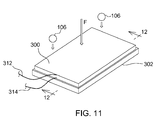
- Figure 11 illustrates a first configuration of a particulate matter impact sensor 301 (e.g. a grain loss sensor).
- a sensing media layer 300 is bonded to a support layer 302.
- the sensing media layer 300 has a first surface 304 that faces the direction of grain flow "F".
- the sensing media layer 300 has a second surface 306 on the opposite side of the sensing media layer that faces away from the direction of grain flow "F”.
- the second surface 306 is bonded to a first surface 308 of the support layer 302.
- the first surface 308 of the support layer 302 faces the direction of grain flow "F”.
- the support layer 302 has a second surface 310 that faces away from the direction of grain flow "F”.
- the sensing media layer 300 is responsive to impacts by seeds 106 traveling in the direction "F" of grain flow. In response to the impacts by seeds 106, the sensing media layer 300 produces an electrical signal at one or more electrical connections 312, 314. The electrical connections 312, 314 are electrically coupled to the sensing media layer 300.
- the function of the support layer 302 is to support the sensing media layer 300.
- a fastening means is used to attach the support layer 302 to the sensing media layer 300.
- the fastening means comprises an adhesive disposed between the second surface 306 to the first surface 308.
- the fastening means comprises a frame extending about the periphery of the sensing media layer.
- the fastening means comprises a plurality of spaced up mechanical fasteners such as screws, rivets, bolts, nuts, and clips that extend between and/or through the support layer 302 and the sensing media layer 300.
- the support layer 302 and the sensing media layer 300 are formed integral with each other.
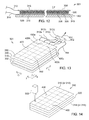
- Figure 12 illustrates a first configuration of the sensing media layer 300.
- the sensing media layer 300 has an upper conductive layer 316, a lower conductive layer 318, and an impact responsive layer 320.
- the upper conductive layer 316 conducts electricity to or from one surface of the impact responsive layer 320 to the electrical connection 314.
- the lower conductive layer 318 conducts electricity to or from an opposing surface of the impact responsive layer 320 to the electrical connection 312.
- the impact responsive layer 320 comprises a pressure responsive media that changes its electrical characteristics upon the impact of the seed 106.
- the electrical characteristics may comprise a change in resistivity, a change in capacitance, or a production of electricity caused by the impact of the seed 106. These electrical characteristics are changed locally in the impact responsive layer 320 immediately adjacent to the location of the seed impact.
- Typical pressure responsive media includes such things as electromechanical films, cellular polymers, polymer electrets, piezoelectric polymers, piezoelectric films, and quasi-piezoelectric films.
- the impact responsive layer 320 comprises a cellular polymer sensing media.
- This material is formed as a thin polypropylene sheet having a cellular structure. This material is manufactured by stretching a polypropylene preform in longitudinal and transverse directions. The stretched sheet is then charged by a corona discharge method. The stretched sheet is full tiny gas voids or "cells" extending in a longitudinal and transverse direction. These cells are separated from one another by leaf-like polypropylene layers. The cells can be compared to large electrical dipoles that are easily compressed in a thickness direction by an externally applied force. The change in thickness at the site of the compression (in our case, the impact site of the seed 106) modifies the dimensions of the dipoles which generates a corresponding electrical charge.
- the biaxial stretching and cellular nature of the material causes the cellular polymer media to respond to compression of the media in a direction normal to the planar extent of the media.
- it also causes the media to be relatively nonresponsive to shear forces applied to the surface of the media.
- cellular polymer sensing media can have a 100-fold reduced sensitivity to shearing forces (i.e. sliding contact) as opposed to normal forces (i.e particle impacts normal to the surface of the media).
- the impact responsive layer 320 comprises a polar piezoelectric polymer (e.g. polyvinylidenefluoride or PVDF) that generates an electrical charge upon impact.
- a polar piezoelectric polymer e.g. polyvinylidenefluoride or PVDF
- the impact responsive layer 320 comprises a material that changes its electrical resistance upon impact and compression, such as molybdenum disulfide-based inks, or conductive coating products such as the "Cho-Shield” line provided by Parker-Chomerics of Woburn, MA.
- the impact responsive layer 320 comprises polymer composites that further comprise polymers (e.g. polymers with polarizable moieties such as polyimides, polyamides, silicon-based polymers, vinyl polymers, polyurethanes, polyureas, polythioureas, polyacrylates, polyesters and/or biopolymers) to which carbon nanotubes (e.g. single wall nanotubes and multiwall nanotubes) have been added, or to which electroceramic particles (e.g. lead-zirconium titanate, lanthanum-modified lead-zirconate titanate, niobium-modified lead-zirconate titanate and/or barium titanate) or to which both have been added.
- polymers e.g. polymers with polarizable moieties such as polyimides, polyamides, silicon-based polymers, vinyl polymers, polyurethanes, polyureas, polythioureas, polyacrylates, polyesters and/or biopolymers
- the upper conductive layer 316 and the lower conductive layer 318 may comprise a film base (e.g. a polyimide (e.g. Kapton), BiPEt (e.g. Mylar, Melinex, Hostaphan), polyester or PTFE (polytetrafluoroethylene) (e.g. Teflon) to which a conductive media (e.g. metals such as aluminum, silver, or gold; or conductive oxides such as indium tin oxide; or carbon such as carbon nanotubes or graphene) is deposited by a sputter-, vapor- or plasma-deposition process (with or without post-deposition annealing or curing).
- a film base e.g. a polyimide (e.g. Kapton), BiPEt (e.g. Mylar, Melinex, Hostaphan), polyester or PTFE (polytetrafluoroethylene) (e.g. Teflon) to which a conductive media (e.g.
- a surface of the upper conductive layer 316 in the lower conductive layer 318 to which the conductive media is applied is then bonded to the impact responsive layer 320.
- This arrangement has the benefit of providing an outwardly facing (e.g. the surface facing seeds 106) polymer layer that provides strength, flexibility, and durability, yet covers and protects a more fragile conductive media.
- the upper conductive layer 316 and the lower conductive layer 318 are continuous and homogeneous over substantially the entire surface of the impact responsive layer. This is particularly beneficial when used to detect random impacts of particulate matter.
- the particular matter impacts random locations on the surface of the sensor. Grain falls from the threshing and separating section of a combine in essentially a random pattern over the surface of the grain impact sensor. It is not directed to a particular region of the grain impact sensor. Each particle has its own random and unpredictable velocity and location as it falls into the surface of the grain impact sensor. As a result, there is no way to predict the point of impact of any particle.
- substantially the entire surface of the particulate matter sensor is preferably equally responsive to impacts of particles.
- the upper conductive layer 316 and the lower conductive layer 318 preferably do not vary in their conductive characteristics over the entire surface of the grain impact sensor. If grain impact occurs at a random location (X, Y) on grain impact sensor and an identical grain impact occurs at a location even as little as 1 mm away from the location (X, Y), an identical electrical change (e.g. a change in resistivity, capacitance, or electrical charge) should be generated by the impact responsive layer 320 and that identical electrical change should be identically communicated through the upper conductive layer 316 in the lower conductive layer 318 to a signal processing circuit. The conveyance of this identical electrical change through the upper conductive layer 316 and the lower conductive layer 318 is enhanced by the continuous and homogeneous characteristics of the upper conductive layer 316 and the lower conductive layer 318 over substantially the entire surface of the grain impact sensor.
- the thickness of the upper conductive layer 316 and the lower conductive layer 318 is generally between 7 and 25 urn.
- “Dynamic mass” refers to the mass of the sensor that is moved in order to cause an electrical change sufficient to indicate a grain impact.
- “Dynamic volume” refers to the volume of the sensor that is moved in order to cause an electrical change sufficient to indicate a grain impact.
- seed-to-sensor mass ratio refers to the mass of the seed making an impact divided by the dynamic mass of the sensor due to that impact.
- the impact of a single seed 106 flexes substantially the entire impact plate 102 and piezoelectric sensing element 114 in order to generate an electrical signal.
- the impact plate 102 and the piezoelectric sensing element 114 can typically have a mass that is 20 to 100 times as great as the seed itself - i.e. a seed-to-sensor mass ratio of 0.05 to 0.01.
- a seed-to-sensor mass ratio of 0.05 to 0.01.
- the impact of the seed 106 against the impact plate 102 is substantially damped and dissipated.
- the kinetic energy of movement of the seed 106 must be converted into a flexure of a much larger mass (the impact plate 102 + the piezoelectric sensing element 114).
- the dynamic mass of the particulate matter impact sensor 301 is significantly smaller.
- the dynamic mass of the particulate matter impact sensor 301 is less than the mass of the particles whose impacts are being sensed by the particulate matter impact sensor 301.
- a corn seed has a mass of about 1000 mg
- a soybean seed has a mass of about 800 mg
- a barley seed has a mass of about 75 mg
- wheat seed has a mass of about 60 mg.
- These seeds 106 are rounded, generally spherical, ovoid, or oblate, and have an overall size of 4 mm to 10 mm.
- a typical seed 106 may impact and deflect and/or compress a small surface area (2 mm 2 to 10 mm 2 ) of the sensing media layer 300 to a depth typically ranging between 25 and 250 urn.
- the depth of this depression depends upon the thickness of the sensing media layer 300, the thickness any protective film layer of that may be provided in front of the sensing media layer 300, and the thickness of any intermediate layer (not shown) that may be disposed between the sensing media layer 300 and the support layer 302.
- This intermediate layer may comprise an adhesive layer provided to attach the sensing media layer 300 to the support layer 302.
- the mass density of the sensing media layer 300 can be approximated as 1.3 g/cm 3 .
- the sensing media layer is impacted by the seed 106 and is compressed only slightly, e.g. to a depth of 25 ⁇ m, and that this compression occurs over of surface area of 2 mm 2 , the dynamic mass of the particulate matter impact sensor 301 is approximately 17 ⁇ g.
- seed 106 is a corn kernel having a mass of 1 g, this arrangement provides a seed-to-sensor mass ratio of 1g/17 ⁇ g or approximately 60,000.
- the sensing media layer is impacted by the seed 106 and is compressed significantly more, e.g. to a depth of 250 ⁇ m over a 10 mm 2 surface area.
- the dynamic mass of the particulate matter impact sensor 301 is approximately 850 ⁇ g.
- seed 106 is a corn kernel having a mass of 1 g, this arrangement provides a seed-to-sensor mass ratio of 1g/850 ⁇ g or approximately 1200.
- the dynamic mass of a traditional grain impact sensor (e.g. the one illustrated in Figures 1-10 ) is 27 g and the dynamic volume is 21 cm 3 .
- these estimates are based upon an impact plate 102 made of plastic, having a thickness of 2 mm, a width of 7 cm, and a length of 15 cm.
- the particulate matter impact sensor 301 has a seed-to-sensor mass ratio greater than 5, alternatively greater than 50, alternatively greater than 500 and alternatively greater than 5000.
- Figure 13 shows a first alternative construction of the particulate matter impact sensor 301 in which support layer 302 similarly supports a particulate matter impact sensor 301 as described above.
- the upper conductive layer 316 has been divided into a plurality of separate, electrically discontinuous, regions 400 (shown in Figure 13 as 400, 400a, 400b, et seq.).
- each of the electrically discontinuous regions (i.e. electrodes) 400 are illustrated in Figure 13 as dashed lines. In Figure 13 , there are 28 of these regions. The regions are discontinuous in a lateral direction "L” and in a direction “O" that is orthogonal to the lateral direction "L".
- the lateral direction “L” is oriented perpendicular to the direction of travel of the agricultural combine on which the particulate matter impact sensor 301 is mounted.
- Each of the regions 400 of the upper conductive layer 316 has a corresponding electrical connection 312 that is connected to a signal processing circuit 402. For convenience of illustration, only four of these electrical connections 312 are shown (312a, 312b, 312c, and 312d). The other regions 400 are similarly connected to the signal processing circuit 402.
- the lower conductive layer 318 extends, unbroken, across the entire lower surface of the impact responsive layer, and thus provides a common electrical connection to the lower surface of the impact responsive layer 320 for each of the individual regions 400 (400a, 400b, etc.).
- the impact responsive layer 320 extends, unbroken, across the entire lower surface of the impact responsive layer.
- the signal processing circuit 402 is configured to receive the electrical changes (discussed above) separately from each of these regions 400 as they are generated by the impact responsive layer 320. In this manner, the electrical change generated by an impact upon the surface of the particulate matter impact sensor 301 registers on the particular corresponding upper electrical connection (312a, 312b, etc.) and on the common electrical connection 314.
- the signal processing circuit 402 is configured to determine the location of the impact based upon which of the electrical connections 312 (312a, 312b, etc.) generates a signal.
- the signal processing circuit 402 is further configured to generate an output signal on signal line 404 that indicates not only the occurrence of an impact, but also the particular region 400 (400a, 400b, etc.) of the regions 400 were the impact occurred. In this manner, the signal processing circuit 402 is configured to determine not only (i) the occurrence of an impact, but (ii) the relative( e.g. x,y or L,O) location of the impact on the particulate matter impact sensor 301
- the lower conductive layer 318 is configured as the upper conductive layer 316 is in Figure 13
- the upper conductive layer 316 is configured as the lower conductive layer 318 is in Figure 13
- the sensing media layer 300 is reversed (compared to that in Figure 13 ) such that the lower conductive layer 318 is divided into regions 400 with each region 400 having its own, separate electrical connection 314 to the signal processing circuit 402 and with a single electrical connection 314 extending across the entire top surface of the particulate matter impact sensor 301.
- This second alternative arrangement has the advantage of providing a substantially continuous and unbroken upper conductive layer 316, which is more resistant to repeated impacts of particles on the first surface 304 as compared to the first alternative arrangement shown in Figure 13 . Wherever there are discontinuities in the upper conductive layer 316 (such as gaps between individual regions 400) it is possible that the upper conductive layer 316 will delaminate from the impact responsive layer 320.
- both the lower conductive layer 318 and the upper conductive layer 316 are divided into regions 400.
- individual electrical connections 312, 314, both upper and lower, to each region 400 are provided.
- an electrical connection 312 connecting to the upper surface and electrical connection 314 connected to the lower surface of that region, and that region alone, is provided for each of the regions 400 of the particulate matter impact sensor 301 and are connected to the signal processing circuit 402.
- the individual regions 400 of the upper conductive layer 316 and/or the lower conductive layer 318 for any of these three alternative arrangements can be provided in a variety of ways.
- the particulate matter impact sensor 301 can be formed as shown in Figure 12 , with a continuous upper conductive layer 316 and a continuous lower conductive layer 318 that are bonded to the impact responsive layer 320. These continuous layers can then be divided into independent regions 400 by removing the conductive material from between each adjacent region 400. This removal would follow (for example) the dashed lines shown in Figure 12 (and shown in Figure 13 as dashed lines 504). In this manner, either the upper conductive layer 316, the lower conductive layer 318, or both of the conductive layers can be segmented into separate regions 400. This can be done, for example, by a laser 500 emitting a computer steerable laser beam 502 following the dashed lines 504 (see Figure 14 ) that mark the divisions between individual regions 400.
- This first process has the advantage of permitting the manufacture of a standard, uniform, and large web of material having an upper conductive layer 316, a lower conductive layer 318, and an impact responsive layer 320, and then permitting it to be cut to reduced dimensions that fit particular particulate matter impact sensor 301, then dividing either (or both) of the upper conductive layer 316 and the lower conductive layer 318 into custom regions 400 for a particular application.
- the impact responsive layer 320 can be provided, and the upper conductive layer 316 and the lower conductive layer 318 (or both) can be applied as a coating on the impact responsive layer 320 in the form of separate regions 400.
- This coating can be done, for example, by screenprinting of conductive materials such as conductive inks, vapor deposition of conductive material (e.g. conductive oxides such as indium tin oxide or carbon such as graphene), or plasma spray deposition of conductive material (e.g. conductive oxides or carbon).
- a screen, mask, or stencil can be disposed between the source of the conductive material and the impact responsive layer 320 itself during the coating process to ensure that separate regions 400 are produced on the surface of the impact responsive layer 320.
- non-coated, non-conductive regions are provided (for example) where the dashed lines appear in Figure 13 by the interposition of the screen, mask, or stencil between the source of the coating and the impact responsive layer 320.
- the upper conductive layer 316 and/or the lower conductive layer 318 can be provided as a continuous conductive layer on an inner surface of a film base (as described above in the section entitled "Conductive Layers") and then selectively removed from the film base using the first process to thereby define the regions 400.
- This film base (with regions 400 defined thereon) can then be fixed to the impact responsive layer 320.
- the upper conductive layer 316 and/or the lower conductive layer 318 can be applied as individual regions 400 on a film base (as described above in the section entitled "Conductive Layers") either directly or with an interposed screen, mask, or stencil.
- This film base (with regions 400 defined thereon) can then be fixed to the impact responsive layer 320.
- Some particulate sensing environments may damage the particulate matter impact sensor 301.
- the particulate matter impact sensor 301 may experience many thousands of seed impacts every minute, (depending upon where the particulate matter impact sensor 301 is located within an agricultural vehicle).
- Monocotyledon seeds 106 such as corn or maize have a sharp stalk at one end that is particularly abrasive when it impacts the particulate matter impact sensor 301.
- FIG. 15 and Figure 16 One arrangement of the particulate matter impact sensor 301 with a protective layer 600 is shown in Figure 15 and Figure 16.
- the protective layer 600 is fixed to the particulate matter impact sensor 301.
- the protective layer 600 substantially covers the upper conductive layer 316, thereby protecting it against wear and erosion.
- the protective layer 600 deforms (i.e. flexes inward), bending the upper conductive layer 316 underneath it, which in turn deforms the impact responsive layer 320 and compresses the impact responsive layer 320 against the lower conductive layer and the support layer 302.
- the protective layer 600 comprises a plastic laminate.
- the plastic laminate may comprise a fiber reinforced plastic.
- the fiber reinforced plastic may comprise a glass fiber reinforced plastic or a carbon fiber reinforced plastic.
- the glass fiber reinforced plastic may comprise a chopped fiber and resin laminate or it may comprise a woven fiber cloth embedded in an epoxy resin binder.
- the woven fiber cloth that is embedded in an epoxy resin binder may comprise National Electrical Manufacturer Association (NEMA) FR-4 grade material or NEMA G-10 grade material.
- NEMA National Electrical Manufacturer Association
- the thickness of the protective layer 600 is in the range of 0.1 to 1.0 mm when using FR-4 grade or G-10 grade material.
- the protective layer 600 comprises plastic.
- the plastic may comprise a polyester material.
- the plastic may comprise polyethylene terephthalate (PET).
- the protective layer 600 comprises a metal.
- the metal may comprise a light metal, e.g. aluminum or an aluminum alloy, or a heavier metal, e.g. steel.
- the protective layer when made from G-10 or FR-4, has a thickness of 0.1 to 1.0 mm. Alternatively it has a thickness 0.15 to 0.8 mm. Alternatively it has a thickness of 0.2 to 0.6 mm. When made of other materials, the protective layer 600 has a thickness sufficient to provide an equivalent flexural rigidity as the flexural rigidity of the protective layer of G-10 or FR-4 with the stated thickness ranges.
- the protective layer 600 is fixed to the particulate matter impact sensor 301 with an adhesive layer 602 that is disposed between the protective layer 600 and the upper conductive layer 316.
Landscapes
- General Physics & Mathematics (AREA)
- Physics & Mathematics (AREA)
- Engineering & Computer Science (AREA)
- Chemical & Material Sciences (AREA)
- Food Science & Technology (AREA)
- Health & Medical Sciences (AREA)
- Life Sciences & Earth Sciences (AREA)
- Biochemistry (AREA)
- Medicinal Chemistry (AREA)
- Analytical Chemistry (AREA)
- General Health & Medical Sciences (AREA)
- Immunology (AREA)
- Pathology (AREA)
- Fluid Mechanics (AREA)
- Power Engineering (AREA)
- Force Measurement Appropriate To Specific Purposes (AREA)
- Laminated Bodies (AREA)
- Investigating Strength Of Materials By Application Of Mechanical Stress (AREA)
- Pressure Sensors (AREA)
- Measurement Of Mechanical Vibrations Or Ultrasonic Waves (AREA)
Abstract
a support layer (302); and
a sensing media layer (300) disposed in front of the support layer (302).
Description
- The invention relates to particulate matter impact sensors. More particularly it relates to grain impact sensors for agricultural harvesters.
- Agricultural harvesters, such as combines, separate crop plants from the ground, thresh the crop plants, separate the grain from the remainder of the crop plants, deposit the remainder the crop plants (MOG) on the ground, and store the grain in a grain reservoir or tank. Periodically, the grain in the grain reservoir is offloaded to a cart or truck that travels alongside the agricultural harvester and is carried away for storage.
- There are several mechanisms inside the agricultural harvester that are used to separate the grain from the MOG. To ensure their proper settings and operation, the performance of various subsystems must be monitored. One way of monitoring the performance of these agricultural harvester subsystems is by determining how much grain passes through particular mechanisms within the agricultural harvester.
- One way of monitoring the passage of grain is by use of a particulate matter impact sensor. These impact sensors are typically called "grain sensors" or "grain loss sensors". These types of sensors are configured to sense the impact of a falling kernel of grain upon a surface of the sensor, and to convert this impact into an electrical signal. This raw electrical signal is then processed and transmitted to an ECU for further use.
- This use can be as simple as displaying the amount (or relative amount) of grain impacting the sensor. With this information alone, an operator, based on his experience, can adjust the machine manually to improve performance. Alternatively, the use can be or complex, such as by employing the signal to automatically adjust the operating settings of various internal mechanisms of the agricultural harvester.
- A common grain loss sensor design in agricultural harvesters comprises a flat impact plate, generally rectangular, to which a sensing element is attached on the rear side of the impact plate. The grain impacts the front side of the impact plate, causing the impact plate to flex.
- A sensing element (typically a piezoelectric sensing element in the form of a thin layer) is attached to the back side of the plate. When the plate flexes, it causes the sensing element on the backside the plate flex in a similar manner. The sensing element, in turn, is coupled to sensing circuits that receive the minute electrical signals from these flexures. The sensing circuits amplify and filter these signals, and convert them into a form that is usable by a digital microprocessor.
- The common grain loss sensor design suffers from several defects. Some of these defects are due to the characteristics of the piezoelectric sensing element itself, and some of them are due to the inhomogeneity of the design overall.
- Piezoelectric sensing elements mounted as described above, generate minute electrical signals based upon the gross bending of the sensor element rather than the localized bending at the point of impact of the kernel of grain upon the impact plate. The impact plate is typically made of relatively rigid material, such fiber reinforced plastic, aluminum, or steel that is a few millimeters thick. The kernels of grain contact perhaps a 10 mm2 area of the impact plate. The impact plate, due to its stiffness, however, does not flex locally in response to the impact. Instead, each grain impact causes substantially the entire impact plate to bend inwardly an infinitesimal distance causing an extremely small curvature of the impact plate.
- One example of a prior art arrangement can be seen in
Figures 1-2 , the dynamic response of which is discussed below. - In
Figure 1 , a shallow metal housing orbox 100 is fixed to animpact plate 102. Theimpact plate 102 has anouter surface 104 against which grains of crop, such assoybeans 106,corn kernels 108, andwheat 110 impact. It has aninside surface 112 two which is bonded apiezoelectric sensing element 114. Asignal conditioning circuit 116 is fixed to thesensing element 114. A signal lead 118 is fixed to the signal conditioning circuit to provide it with electrical power and to receive back conditioned signals. These signals are received by an ECU/DSP for further processing and use. - The
impact plate 102 is fixed at its edges to the edges of theshallow metal housing 100. It may be fixed withmechanical fasteners 120 such as rivets, bolts, screws, etc., or anadhesive 122. The edges of theimpact plate 102 are therefore constrained in their movement by being fixed and/or coupled to the edges of theshallow metal housing 100. Theimpact plate 102 is homogeneous in construction in that it has a constant thickness and constant material characteristics over substantially its entire extent. - The
impact plate 102 is large compared to the size of the seeds that contact it. Theimpact plate 102 typically ranges from 75 mm x 75 mm to 125 mm x 250 mm. - The
sensing element 114 does not extend over the entire inner surface of theimpact plate 102. Grain can contact theimpact plate 102 at any oflocations 124, for example, that is disposed away from thesensing element 114. In order to communicate this impact to thesensing element 114 itself, theentire impact plate 102 must flex in response. - To illustrate this effect, an exaggerated view of this flexure in response to shown in
Figures 3-5 . - In
Figure 3 , theseed 106 is approaching theimpact plate 102 at a velocity "V". The seed approaches theimpact plate 102 at the center of the plate, equidistant from all the edges of the plate. Theimpact plate 102 has thesensing element 114 attached to itsinner surface 112. The edges of thehousing 100 that support the edges of theimpact plate 102 are shown schematically as ground symbols. They are fixed and stationary. - In
Figure 4 , theseed 106 has just contacted theimpact plate 102. Given the deformation of the typical seed at a velocity "V", the contact area is approximately 2 mm x 2 mm. - In
Figure 5 , theseed 106 has transferred all of its kinetic energy into theimpact plate 102 and has slowed to a stop. Theimpact plate 102 has stored the kinetic energy of theseed 106 by elastic deformation. Theimpact plate 102 has flexed inward, becoming concave on itsouter surface 104 and convex on itsinner surface 112. - In
Figure 5 , theimpact plate 102 has flexed inward an amount "D". This inward flexure of theimpact plate 102 has caused the corresponding and substantially equal flexure of thesensing element 114. Since thesensing element 114 disposed on the back of theimpact plate 102, it is stretched in a direction "X" that is generally parallel to the plane of thesensing element 114. It is also flexed into a similar concave shape as theimpact plate 102 since it is bonded to theinner surface 112 of theimpact plate 102. This stretching and flexure of thesensing element 114 effects substantially the entire area of thesensing element 114. - In
Figure 6 , the energy stored in theimpact plate 102 and thesensing element 114 has been released and theseed 106 has been propelled in the reverse direction. Theimpact plate 102 has returned to its initial position (in this case, generally flat) as well as thesensing element 114. The electrical signal that was produced by the flexure of thesensing element 114 has disappeared since thesensing element 114 has returned to its initial, and stressed, shape. - In
Figure 7 , theimpact plate 102 and thesensing element 114 continues moving in the reverse direction until both have achieved a convex configuration. In order to get a fast response, and loss sensors are underdamped, which permits them to oscillate convex> concave > convex > concave as the energy input by theseed 106 dissipates. As this oscillation occurs, the signal from thesensing element 114 continues This "ringing" of the sensor occurs at a relatively low natural frequency, often taking 10 or 15 ms to decay. In an overdamped sensor arrangement, theseed 106 would bounce off the (concave) outer surface 104 (Figure 5 ) and theimpact plate 102 and thesensing element 114 would gradually return to their planar position (as shown inFigure 6 ) without achieving the convex position shown inFigure 7 . In this situation, the gradual restitution of thesensing element 114 to its initial planar shape would cause a gradual falloff of the signal produced by thesensing element 114. As in the case of the underdamped system, this gradual signal falloff can take 5 to 10 ms. - The 5 to 10 ms decay of the signal from the
sensing element 114 has been determined to be a function of its overall size, mass, and stiffness. - The description above illustrates the ideal situation in which a
seed 106 impacts the center of theimpact plate 102 causing equal deflection of theimpact plate 102 and thesensing element 114 in all directions. Given the symmetry in all directions about the center contact point of theseed 106 against the impact plate, the physical characteristics of theimpact plate 102 and thesensing element 114 mandate that the response will be generally are shown inFigures 3-7 . - In the real world, however, substantially the entire
outer surface 104 of theimpact plate 102 can be impacted by theseed 106. When an off-center impact by theseed 106 occurs, the characteristics of the resultant signal changes in unpredictable ways. An off-center impact of theseed 106 against theimpact plate 102 is illustrated inFigures 8-10 . - In
Figure 8 , for example, aseed 106 approaches theimpact plate 102 in a position that is off-center and adjacent to the edge of theimpact plate 102. Theimpact plate 102 is supported on all sides by thehousing 100. As in the examples ofFigures 3-7 , thehousing 100 is represented as a ground symbol for convenience of illustration. - In
Figure 9 , theseed 106 has contacted theimpact plate 102 and has deflected it inward in the region surrounding the point of impact. Since the point of impact is off-center and immediately adjacent to thehousing 100 which supports theimpact plate 102, the movement of the impact plate is constrained. Theimpact plate 102 can no longer flex symmetrically across substantially its entire surface. Instead, as the energy of theseed 108 is absorbed by theimpact plate 102, theimpact plate 102 is deflected into a second mode of oscillation in which aportion 200 of the plate adjacent to theseed 106 is flexed into a concave shape, and aportion 202 of theimpact plate 102 away from theseed 106 is flexed into a convex shape. Similarly, thesensing element 114, which is disposed in a center region of the impact plate 102) reproduces a similar convex/concave flexure. - The distance "D" of the concave flexure is smaller than the distance "D" of the concave flexure for a center impact (see
Figure 5 ) since the seed one impacted theimpact plate 102 adjacent to fixed support (i.e. the edge of theimpact plate 102 where it is fixed rigidly to theshallow housing 100. since the distance "D" is reduced for a seed impact adjacent to an edge of theimpact plate 102 as compared to a seed impact in the center of theimpact plate 102, thesensing element 114 flexes much less, and therefore generates a much smaller electrical signal for impacts adjacent to the edge. This change in signal amplitude based upon the position of the seed impact on the surface of theimpact plate 102 makes it difficult to properly condition the signal. - The signal problem is further complicated since the sensing element generates a signal related to its degree of stretching and its flexure. The
portion 204 of thesensing element 114 adjacent to the seed and is under tension - it is stretched. However, theportion 206 of thesensing element 114 on the other side of the grain loss sensor is compressed. The signal produced by thesensing element 114 is an average of the tension/compression effects across the entire surface area of thesensing element 114. Since thesensing element 114 is experiencing both a tension in oneportion 204 and a compression in anotherportion 206, the electrical signal generated by thesensing element 114 overall is even further reduced, since these two areas generate opposing electrical signals that (in effect) cancel each other out. -
Figure 10 illustrates the oscillation of theimpact plate 102 when theimpact plate 102 plussensing element 114 combination is underdamped after theseed 106 is released. In a typical grain loss sensor of this design, theimpact plate 102 can oscillate back-and-forth between the two extreme positions illustrated inFigure 10 . In this case, theimpact plate 102 +sensing element 114 will gradually return to the position shown inFigure 8 as their energy is dissipated. This can take 5 to 10 ms. - Alternatively, if the
impact plate 102 plussensing element 114 combination is overdamped, it will release theseed 106 in the position shown inFigure 9 and relax to the generally planar position shown inFigure 8 . Depending on the degree of over damping, this gradual return to the position shown inFigure 9 can take 5 to 10 ms. - A further complication is the difference in vibrational frequencies generated by the seed one impact of
Figures 3-7 and theseed 106 impact ofFigures 8-10 . When theimpact plate 102 oscillates in its primary mode (shown inFigures 3-7 ) it has a frequency of oscillation that is less than the frequency of oscillation caused by the off-center seed impact shown inFigures 8-10 . This also adds to the complexity and difficulty of determining individual seed impacts. - In the description above regarding
Figures 3-10 , I've illustrated only two different positions at which theseed 106 may impact theimpact plate 102. There are an infinite number of positions at which a seed one can impact theimpact plate 102. Further, the wave equation predicts that there are an infinite number of modes of oscillation that can be generated by each impact, each mode of oscillation having its own distinct (and different) frequency and its own distinct (and different) amplitude. - The final complication in determining seed impacts on a grain loss sensor of this design is when several seeds make contact the impact plate at many different locations on the impact plate within milliseconds of each other. Given the long decay time from a single seed impact (5-10 ms), it is virtually impossible to distinguish individual seed impacts when they are occurring faster than once every 20-30 ms or so. There are so many possible modes of oscillation (based upon the location of the strike), there are so many possible amplitudes (based upon the location of the strike) and there is such a long decay time (because of the large mass of the
sensing element 114 and the impact plate 102) that identifying and quantifying grain strikes with any accuracy is virtually impossible. - One potential solution is to provide many more of these grain loss sensors and arranging them side-by-side, each of these grain loss sensors having a smaller impact plate. The costs of doing this are high, however.
- Another potential solution is to have a single
large impact plate 102, but to bond multiple,smaller sensing elements 114 in an array on the back of theimpact plate 102. This, too, would be quite costly. The number of electrical interconnections that would have to be made to each individual sensor would be prohibitive. Further, each sensor would still generate a signal that was a composite of the effects of grain strikes all over the sensor plate since the oscillations of theimpact plate 102 would still be communicated through the impact plate from the point of impact to other adjacent regions of theimpact plate 102. Separating out spurious components of the signal from onesensing element 114 due to grain strikes on a distant portion of theimpact plate 102 would be virtually impossible. Finally, as the number of thesensing elements 114 bonded to the back of theimpact plate 102 is increased, the size of eachsensing element 114 would have to be correspondingly reduced. The reduced size of eachsensing element 114 would cause a corresponding reduction in signal amplitude which would thus make eachsensing element 114 much less sensitive and much more subject to electrical and mechanical noise. - What is needed, therefore, is a sensor arrangement that is faster, that has less noise, that has a higher frequency of response, and/or has a lower dynamic mass. It is an object of this invention to provide such a sensor arrangement.
- This new sensor arrangement embodies several inventions. This new sensor arrangement has several different embodiments.
-
Figure 11 illustrates a first configuration of a particulate matter impact sensor 301 (e.g. a grain loss sensor). In this arrangement, asensing media layer 300 is bonded to asupport layer 302. Thesensing media layer 300 has afirst surface 304 that faces the direction of grain flow "F". Thesensing media layer 300 has asecond surface 306 on the opposite side of the sensing media layer that faces away from the direction of grain flow "F". Thesecond surface 306 is bonded to afirst surface 308 of thesupport layer 302. Thefirst surface 308 of thesupport layer 302 faces the direction of grain flow "F". Thesupport layer 302 has asecond surface 310 that faces away from the direction of grain flow "F". - The
sensing media layer 300 is responsive to impacts byseeds 106 traveling in the direction "F" of grain flow. In response to the impacts byseeds 106, thesensing media layer 300 produces an electrical signal at one or moreelectrical connections electrical connections sensing media layer 300. - The function of the
support layer 302 is to support thesensing media layer 300. A fastening means is used to attach thesupport layer 302 to thesensing media layer 300. In one arrangement, the fastening means comprises an adhesive disposed between thesecond surface 306 to thefirst surface 308. In another arrangement the fastening means comprises a frame extending about the periphery of the sensing media layer. In another arrangement, the fastening means comprises a plurality of spaced up mechanical fasteners such as screws, rivets, bolts, nuts, and clips that extend between and/or through thesupport layer 302 and thesensing media layer 300. In another arrangement, thesupport layer 302 and thesensing media layer 300 are formed integral with each other. -
Figure 12 illustrates a first configuration of thesensing media layer 300. In this arrangement, thesensing media layer 300 has an upperconductive layer 316, a lowerconductive layer 318, and an impactresponsive layer 320. - The upper
conductive layer 316 conducts electricity to or from one surface of the impactresponsive layer 320 to theelectrical connection 314. - The lower
conductive layer 318 conducts electricity to or from an opposing surface of the impactresponsive layer 320 to theelectrical connection 312. - The impact
responsive layer 320 comprises a pressure responsive media that changes its electrical characteristics upon the impact of theseed 106. The electrical characteristics may comprise a change in resistivity, a change in capacitance, or a production of electricity caused by the impact of theseed 106. These electrical characteristics are changed locally in the impactresponsive layer 320 immediately adjacent to the location of the seed impact. Typical pressure responsive media includes such things as electromechanical films, cellular polymers, polymer electrets, piezoelectric polymers, piezoelectric films, and quasi-piezoelectric films. - In one particular arrangement the impact
responsive layer 320 comprises a cellular polymer sensing media. This material is formed as a thin polypropylene sheet having a cellular structure. This material is manufactured by stretching a polypropylene preform in longitudinal and transverse directions. The stretched sheet is then charged by a corona discharge method. The stretched sheet is full tiny gas voids or "cells" extending in a longitudinal and transverse direction. These cells are separated from one another by leaf-like polypropylene layers. The cells can be compared to large electrical dipoles that are easily compressed in a thickness direction by an externally applied force. The change in thickness at the site of the compression (in our case, the impact site of the seed 106) modifies the dimensions of the dipoles which generates a corresponding electrical charge. - The biaxial stretching and cellular nature of the material causes the cellular polymer media to respond to compression of the media in a direction normal to the planar extent of the media. Advantageously, it also causes the media to be relatively nonresponsive to shear forces applied to the surface of the media. In fact, cellular polymer sensing media can have a 100-fold reduced sensitivity to shearing forces (i.e. sliding contact) as opposed to normal forces (i.e particle impacts normal to the surface of the media).
- This is of particular benefit for grain loss sensors that are disposed normal to a path of incoming, falling grain or other particulate matter. Grain (or other particulate matter) impacting the surface of the sensor normal to the longitudinal and transverse extent of the impact responsive layer will generate a strong signal upon initial (normal) impact. As those same particles slide down the face of the sensor after impact, the shear forces generated by the sliding of the particles will generate a corresponding electric charge with a greatly reduced. This will innately reduce or eliminate the signals generated from second impacts and sliding movement of the particulate matter after the initial impact. In this manner, double (or triple) counts of each seed impact can be reduced or eliminated and therefore the number of tool particles contacting the sensor can be more accurately counted.
- In another arrangement, the impact
responsive layer 320 comprises a polar piezoelectric polymer (e.g. polyvinylidenefluoride or PVDF) that generates an electrical charge upon impact. - In another arrangement the impact
responsive layer 320 comprises a material that changes its electrical resistance upon impact and compression, such as molybdenum disulfide-based inks, or conductive coating products such as the "Cho-Shield" line provided by Parker-Chomerics of Woburn, MA. - In another arrangement, the impact
responsive layer 320 comprises polymer composites that further comprise polymers (e.g. polymers with polarizable moieties such as polyimides, polyamides, silicon-based polymers, vinyl polymers, polyurethanes, polyureas, polythioureas, polyacrylates, polyesters and/or biopolymers) to which carbon nanotubes (e.g. single wall nanotubes and multiwall nanotubes) have been added, or to which electroceramic particles (e.g. lead-zirconium titanate, lanthanum-modified lead-zirconate titanate, niobium-modified lead-zirconate titanate and/or barium titanate) or to which both have been added. See, for example, published patent applicationUS 2006/0084752 A1 , which is incorporated herein by reference for all that it teaches. - In one arrangement, the upper
conductive layer 316 and the lowerconductive layer 318 may comprise a film base (e.g. a polyimide (e.g. Kapton), BiPEt (e.g. Mylar, Melinex, Hostaphan), polyester or PTFE (polytetrafluoroethylene) (e.g. Teflon) to which a conductive media (e.g. metals such as aluminum, silver, or gold; or conductive oxides such as indium tin oxide; or carbon such as carbon nanotubes or graphene) is deposited by a sputter-, vapor- or plasma-deposition process (with or without post-deposition annealing or curing). In this arrangement, a surface of the upperconductive layer 316 in the lowerconductive layer 318 to which the conductive media is applied is then bonded to the impactresponsive layer 320. This arrangement has the benefit of providing an outwardly facing (e.g. the surface facing seeds 106) polymer layer that provides strength, flexibility, and durability, yet covers and protects a more fragile conductive media. - In one arrangement, the upper
conductive layer 316 and the lowerconductive layer 318 are continuous and homogeneous over substantially the entire surface of the impact responsive layer. This is particularly beneficial when used to detect random impacts of particulate matter. In the present case (i.e. that of a grain impact sensor) the particular matter impacts random locations on the surface of the sensor. Grain falls from the threshing and separating section of a combine in essentially a random pattern over the surface of the grain impact sensor. It is not directed to a particular region of the grain impact sensor. Each particle has its own random and unpredictable velocity and location as it falls into the surface of the grain impact sensor. As a result, there is no way to predict the point of impact of any particle. - To accommodate this virtually infinite number of impact locations, substantially the entire surface of the particulate matter sensor is preferably equally responsive to impacts of particles. Thus, the upper
conductive layer 316 and the lowerconductive layer 318 preferably do not vary in their conductive characteristics over the entire surface of the grain impact sensor. If grain impact occurs at a random location (X, Y) on grain impact sensor and an identical grain impact occurs at a location even as little as 1 mm away from the location (X, Y), an identical electrical change (e.g. a change in resistivity, capacitance, or electrical charge) should be generated by the impactresponsive layer 320 and that identical electrical change should be identically communicated through the upperconductive layer 316 in the lowerconductive layer 318 to a signal processing circuit. The conveyance of this identical electrical change through the upperconductive layer 316 and the lowerconductive layer 318 is enhanced by the continuous and homogeneous characteristics of the upperconductive layer 316 and the lowerconductive layer 318 over substantially the entire surface of the grain impact sensor. - The thickness of the upper
conductive layer 316 and the lowerconductive layer 318 is generally between 7 and 25 urn. - "Dynamic mass" refers to the mass of the sensor that is moved in order to cause an electrical change sufficient to indicate a grain impact.
- "Dynamic volume" refers to the volume of the sensor that is moved in order to cause an electrical change sufficient to indicate a grain impact.
- The "seed-to-sensor mass ratio" refers to the mass of the seed making an impact divided by the dynamic mass of the sensor due to that impact.
- In prior art arrangements (shown in
Figures 1-10 ) the impact of asingle seed 106 flexes substantially theentire impact plate 102 andpiezoelectric sensing element 114 in order to generate an electrical signal. Theimpact plate 102 and thepiezoelectric sensing element 114 can typically have a mass that is 20 to 100 times as great as the seed itself - i.e. a seed-to-sensor mass ratio of 0.05 to 0.01. As the inventors have discovered, and as described above in conjunction withFigures 1-10 , as the seed the sensor mass ratio decreases, the natural frequency of the sensor decreases making it hard to identify individual seed impacts upon the sensor surface. Further, the larger, thinner and more flexible the particulate impact sensor is made, the more modes of vibration are generated in the particulate matter impact sensor, each mode having its own natural frequencies of oscillation, which also makes it difficult to identify anindividual seed 106 impact from the signal generated by the particulate matter impact sensor. - Even if the
seed 106 is traveling at a relatively high speed when it impacts theimpact plate 102, the impact of theseed 106 against theimpact plate 102 is substantially damped and dissipated. The kinetic energy of movement of theseed 106 must be converted into a flexure of a much larger mass (theimpact plate 102 + the piezoelectric sensing element 114). - In comparison to this prior art arrangement, the dynamic mass of the particulate
matter impact sensor 301 is significantly smaller. The dynamic mass of the particulatematter impact sensor 301 is less than the mass of the particles whose impacts are being sensed by the particulatematter impact sensor 301. A corn seed has a mass of about 1000 mg, a soybean seed has a mass of about 800 mg, a barley seed has a mass of about 75 mg, and wheat seed has a mass of about 60 mg. Theseseeds 106 are rounded, generally spherical, ovoid, or oblate, and have an overall size of 4 mm to 10 mm. - Depending upon the resilience of the
sensing media layer 300 and the size and mass of the seed, atypical seed 106 may impact and deflect and/or compress a small surface area (2 mm2 to 10 mm2) of thesensing media layer 300 to a depth typically ranging between 25 and 250 urn. The depth of this depression depends upon the thickness of thesensing media layer 300, the thickness any protective film layer of that may be provided in front of thesensing media layer 300, and the thickness of any intermediate layer (not shown) that may be disposed between thesensing media layer 300 and thesupport layer 302. This intermediate layer may comprise an adhesive layer provided to attach thesensing media layer 300 to thesupport layer 302. - The mass density of the
sensing media layer 300 can be approximated as 1.3 g/cm3. - In one example, assume that the sensing media layer is impacted by the
seed 106 and is compressed only slightly, e.g. to a depth of 25 µm, and that this compression occurs over of surface area of 2 mm2, the dynamic mass of the particulatematter impact sensor 301 is approximately 17 µg. Assuming thatseed 106 is a corn kernel having a mass of 1 g, this arrangement provides a seed-to-sensor mass ratio of 1g/17µg or approximately 60,000. - In another example, assume that the sensing media layer is impacted by the
seed 106 and is compressed significantly more, e.g. to a depth of 250 µm over a 10 mm2 surface area. In this case, the dynamic mass of the particulatematter impact sensor 301 is approximately 850 µg. Assuming thatseed 106 is a corn kernel having a mass of 1 g, this arrangement provides a seed-to-sensor mass ratio of 1g/850µg or approximately 1200. - By way of comparison, the dynamic mass of a traditional grain impact sensor (e.g. the one illustrated in
Figures 1-10 ) is 27 g and the dynamic volume is 21 cm3. These estimates are based upon animpact plate 102 made of plastic, having a thickness of 2 mm, a width of 7 cm, and a length of 15 cm. - To provide optimum performance, the particulate
matter impact sensor 301 has a seed-to-sensor mass ratio greater than 5, alternatively greater than 50, alternatively greater than 500 and alternatively greater than 5000. -
Figure 13 shows a first alternative construction of the particulatematter impact sensor 301 in whichsupport layer 302 similarly supports a particulatematter impact sensor 301 as described above. - In this alternative construction, however, the upper
conductive layer 316 has been divided into a plurality of separate, electrically discontinuous, regions 400 (shown inFigure 13 as 400, 400a, 400b, et seq.). - The boundaries of each of the electrically discontinuous regions (i.e. electrodes) 400 are illustrated in
Figure 13 as dashed lines. InFigure 13 , there are 28 of these regions. The regions are discontinuous in a lateral direction "L" and in a direction "O" that is orthogonal to the lateral direction "L". - The lateral direction "L" is oriented perpendicular to the direction of travel of the agricultural combine on which the particulate
matter impact sensor 301 is mounted. By providingmultiple regions 400 of the particulatematter impact sensor 301 that are oriented adjacent to each other in the direction "L" , the particulatematter impact sensor 301 is capable of determining - Each of the
regions 400 of the upperconductive layer 316 has a correspondingelectrical connection 312 that is connected to asignal processing circuit 402. For convenience of illustration, only four of theseelectrical connections 312 are shown (312a, 312b, 312c, and 312d). Theother regions 400 are similarly connected to thesignal processing circuit 402. - The lower
conductive layer 318 extends, unbroken, across the entire lower surface of the impact responsive layer, and thus provides a common electrical connection to the lower surface of the impactresponsive layer 320 for each of the individual regions 400 (400a, 400b, etc.). Similarly, the impactresponsive layer 320 extends, unbroken, across the entire lower surface of the impact responsive layer. - The
signal processing circuit 402 is configured to receive the electrical changes (discussed above) separately from each of theseregions 400 as they are generated by the impactresponsive layer 320. In this manner, the electrical change generated by an impact upon the surface of the particulatematter impact sensor 301 registers on the particular corresponding upper electrical connection (312a, 312b, etc.) and on the commonelectrical connection 314. Thesignal processing circuit 402 is configured to determine the location of the impact based upon which of the electrical connections 312 (312a, 312b, etc.) generates a signal. Thesignal processing circuit 402 is further configured to generate an output signal onsignal line 404 that indicates not only the occurrence of an impact, but also the particular region 400 (400a, 400b, etc.) of theregions 400 were the impact occurred. In this manner, thesignal processing circuit 402 is configured to determine not only (i) the occurrence of an impact, but (ii) the relative( e.g. x,y or L,O) location of the impact on the particulatematter impact sensor 301. - In a second alternative arrangement similar to that of the arrangement in
Figure 13 , the lowerconductive layer 318 is configured as the upperconductive layer 316 is inFigure 13 , and the upperconductive layer 316 is configured as the lowerconductive layer 318 is inFigure 13 . In other words, thesensing media layer 300 is reversed (compared to that inFigure 13 ) such that the lowerconductive layer 318 is divided intoregions 400 with eachregion 400 having its own, separateelectrical connection 314 to thesignal processing circuit 402 and with a singleelectrical connection 314 extending across the entire top surface of the particulatematter impact sensor 301. This second alternative arrangement has the advantage of providing a substantially continuous and unbroken upperconductive layer 316, which is more resistant to repeated impacts of particles on thefirst surface 304 as compared to the first alternative arrangement shown inFigure 13 . Wherever there are discontinuities in the upper conductive layer 316 (such as gaps between individual regions 400) it is possible that the upperconductive layer 316 will delaminate from the impactresponsive layer 320. - In a third alternative arrangement similar to that of the arrangement in
Figures 12 and 13 , both the lowerconductive layer 318 and the upperconductive layer 316 are divided intoregions 400. To sense electrical changes due to particulate matter impacts in aparticular region 400 of the particulatematter impact sensor 301, individualelectrical connections region 400 are provided. Thus for eachregion 400, anelectrical connection 312 connecting to the upper surface andelectrical connection 314 connected to the lower surface of that region, and that region alone, is provided for each of theregions 400 of the particulatematter impact sensor 301 and are connected to thesignal processing circuit 402. - The
individual regions 400 of the upperconductive layer 316 and/or the lowerconductive layer 318 for any of these three alternative arrangements can be provided in a variety of ways. - In a first process, the particulate
matter impact sensor 301 can be formed as shown inFigure 12 , with a continuous upperconductive layer 316 and a continuous lowerconductive layer 318 that are bonded to the impactresponsive layer 320. These continuous layers can then be divided intoindependent regions 400 by removing the conductive material from between eachadjacent region 400. This removal would follow (for example) the dashed lines shown inFigure 12 (and shown inFigure 13 as dashed lines 504). In this manner, either the upperconductive layer 316, the lowerconductive layer 318, or both of the conductive layers can be segmented intoseparate regions 400. This can be done, for example, by alaser 500 emitting a computer steerable laser beam 502 following the dashed lines 504 (seeFigure 14 ) that mark the divisions betweenindividual regions 400. - This first process has the advantage of permitting the manufacture of a standard, uniform, and large web of material having an upper
conductive layer 316, a lowerconductive layer 318, and an impactresponsive layer 320, and then permitting it to be cut to reduced dimensions that fit particular particulatematter impact sensor 301, then dividing either (or both) of the upperconductive layer 316 and the lowerconductive layer 318 intocustom regions 400 for a particular application. - In a second process, the impact
responsive layer 320 can be provided, and the upperconductive layer 316 and the lower conductive layer 318 (or both) can be applied as a coating on the impactresponsive layer 320 in the form ofseparate regions 400. This coating can be done, for example, by screenprinting of conductive materials such as conductive inks, vapor deposition of conductive material (e.g. conductive oxides such as indium tin oxide or carbon such as graphene), or plasma spray deposition of conductive material (e.g. conductive oxides or carbon). - If in the second process the coatings cannot be selectively applied as
separate regions 400 to the impactresponsive layer 320, then a screen, mask, or stencil can be disposed between the source of the conductive material and the impactresponsive layer 320 itself during the coating process to ensure thatseparate regions 400 are produced on the surface of the impactresponsive layer 320. In other words, that non-coated, non-conductive regions are provided (for example) where the dashed lines appear inFigure 13 by the interposition of the screen, mask, or stencil between the source of the coating and the impactresponsive layer 320. - In a third process, the upper
conductive layer 316 and/or the lowerconductive layer 318 can be provided as a continuous conductive layer on an inner surface of a film base (as described above in the section entitled "Conductive Layers") and then selectively removed from the film base using the first process to thereby define theregions 400. This film base (withregions 400 defined thereon) can then be fixed to the impactresponsive layer 320. - In a fourth process, the upper
conductive layer 316 and/or the lowerconductive layer 318 can be applied asindividual regions 400 on a film base (as described above in the section entitled "Conductive Layers") either directly or with an interposed screen, mask, or stencil. This film base (withregions 400 defined thereon) can then be fixed to the impactresponsive layer 320. - Some particulate sensing environments may damage the particulate
matter impact sensor 301. For example, in agricultural applications, the particulatematter impact sensor 301 may experience many thousands of seed impacts every minute, (depending upon where the particulatematter impact sensor 301 is located within an agricultural vehicle).Monocotyledon seeds 106 such as corn or maize have a sharp stalk at one end that is particularly abrasive when it impacts the particulatematter impact sensor 301. - To prevent excessive damage to the particulate
matter impact sensor 301 it is beneficial to provide one or more protective layers 600 to cover the upperconductive layer 316. One arrangement of the particulatematter impact sensor 301 with a protective layer 600 is shown in Figure 15 and Figure 16. The protective layer 600 is fixed to the particulatematter impact sensor 301. The protective layer 600 substantially covers the upperconductive layer 316, thereby protecting it against wear and erosion. When impacted by particulate matter such as seeds, the protective layer 600 deforms (i.e. flexes inward), bending the upperconductive layer 316 underneath it, which in turn deforms the impactresponsive layer 320 and compresses the impactresponsive layer 320 against the lower conductive layer and thesupport layer 302. - In one arrangement the protective layer 600 comprises a plastic laminate. The plastic laminate may comprise a fiber reinforced plastic. The fiber reinforced plastic may comprise a glass fiber reinforced plastic or a carbon fiber reinforced plastic. The glass fiber reinforced plastic may comprise a chopped fiber and resin laminate or it may comprise a woven fiber cloth embedded in an epoxy resin binder. The woven fiber cloth that is embedded in an epoxy resin binder may comprise National Electrical Manufacturer Association (NEMA) FR-4 grade material or NEMA G-10 grade material. The thickness of the protective layer 600 is in the range of 0.1 to 1.0 mm when using FR-4 grade or G-10 grade material.
- In another arrangement, the protective layer 600 comprises plastic. The plastic may comprise a polyester material. The plastic may comprise polyethylene terephthalate (PET).
- In another arrangement, the protective layer 600 comprises a metal. The metal may comprise a light metal, e.g. aluminum or an aluminum alloy, or a heavier metal, e.g. steel.
- The protective layer, when made from G-10 or FR-4, has a thickness of 0.1 to 1.0 mm. Alternatively it has a thickness 0.15 to 0.8 mm. Alternatively it has a thickness of 0.2 to 0.6 mm. When made of other materials, the protective layer 600 has a thickness sufficient to provide an equivalent flexural rigidity as the flexural rigidity of the protective layer of G-10 or FR-4 with the stated thickness ranges.
- The protective layer 600 is fixed to the particulate
matter impact sensor 301 with an adhesive layer 602 that is disposed between the protective layer 600 and the upperconductive layer 316.
Claims (10)
- A particulate matter impact sensor (301) for sensing impacts of particles (106) comprising:a support layer (302); anda sensing media layer (300) disposed in front of the support layer (302).
- The particulate matter impact sensor (301) of Claim 1, wherein the sensing media layer (300) comprises a sheet with cellular voids.
- The particulate matter impact sensor (301) according to any of the claims herein, wherein the sensing media layer (300) comprises an impact responsive layer (320) having an outer surface facing a direction of material flow and an inner surface facing the support layer (302).
- The particulate matter impact sensor (301) according to any of the claims herein, wherein the sensing media layer (300) has a thickness of no greater than 500 urn.
- The particulate matter impact sensor (301) according to any of the claims herein, wherein the sensing media layer (300) is comprised of biaxially stretched polypropylene.
- The particulate matter impact sensor (301) according to any of the claims herein, further comprising a protective layer (600) that is fixed to the sensing media layer (300) and is located between the particles (106) impacting the particulate matter impact sensor (301) and the sensing media layer (300).
- The particulate matter impact sensor (301) according to Claim 6, wherein the protective layer (600) comprises plastic or metal.
- The particulate matter impact sensor (301) according to Claim 7, wherein the protective layer (600) comprises a plastic laminate.
- The particulate matter impact sensor (301) according to Claim 8, wherein the plastic laminate comprises a fiber reinforced plastic, in particular reinforced with glass fibers or carbon fibers.
- The particulate matter impact sensor (301) according to Claim 7, wherein the protective layer (600) comprises aluminum.
Applications Claiming Priority (2)
| Application Number | Priority Date | Filing Date | Title |
|---|---|---|---|
| US201462027514P | 2014-07-22 | 2014-07-22 | |
| US14/794,089 US10126153B2 (en) | 2014-07-22 | 2015-07-08 | Particulate matter impact sensor |
Publications (3)
| Publication Number | Publication Date |
|---|---|
| EP2977735A2 true EP2977735A2 (en) | 2016-01-27 |
| EP2977735A3 EP2977735A3 (en) | 2016-06-15 |
| EP2977735B1 EP2977735B1 (en) | 2018-02-14 |
Family
ID=53682525
Family Applications (1)
| Application Number | Title | Priority Date | Filing Date |
|---|---|---|---|
| EP15176406.5A Active EP2977735B1 (en) | 2014-07-22 | 2015-07-13 | Particulate matter impact sensor |
Country Status (3)
| Country | Link |
|---|---|
| US (1) | US10126153B2 (en) |
| EP (1) | EP2977735B1 (en) |
| BR (1) | BR102015017370B8 (en) |
Cited By (7)
| Publication number | Priority date | Publication date | Assignee | Title |
|---|---|---|---|---|
| CN106706177A (en) * | 2016-11-11 | 2017-05-24 | 浙江大学 | Double-layered crisscross-structure particle collision sensor based on PVDF (Polyvinylidene Fluoride) |
| DE102017204101A1 (en) | 2017-03-13 | 2018-09-13 | Deere & Company | Grain sensor for a combine harvester |
| CN110715763A (en) * | 2019-11-11 | 2020-01-21 | 西安近代化学研究所 | Shock wave pressure measuring device and method for parallel combined dielectric elastomer |
| WO2020126309A1 (en) * | 2018-12-19 | 2020-06-25 | Agco International Gmbh | Grain cleaning system and method of controlling such |
| WO2024170351A1 (en) * | 2023-02-13 | 2024-08-22 | Technische Universität Darmstadt | Electromechanical converter element |
| EP4454451A1 (en) | 2023-04-25 | 2024-10-30 | Deere & Company | Sensor arrangement for a combine harvester |
| EP4702830A1 (en) | 2024-08-29 | 2026-03-04 | Deere & Company | Sensor arrangement for detecting grains in a crop flow containing grains and material other than grain in a combine harvester |
Families Citing this family (75)
| Publication number | Priority date | Publication date | Assignee | Title |
|---|---|---|---|---|
| JP6652882B2 (en) * | 2016-04-28 | 2020-02-26 | Nissha株式会社 | Pressure detector |
| JP6401735B2 (en) * | 2016-05-12 | 2018-10-10 | 三菱重工業株式会社 | Impact detection laminate, impact detection method, and inspection method for protection object |
| JP6811113B2 (en) * | 2017-02-14 | 2021-01-13 | 株式会社Screenホールディングス | Impact force measuring device, substrate processing device, impact force measuring method, and substrate processing method |
| US10792960B2 (en) * | 2017-12-20 | 2020-10-06 | The Goodyear Tire & Rubber Company | Article with electronic component inclusion |
| US10729067B2 (en) * | 2018-10-20 | 2020-08-04 | Deere & Company | Biomass impact sensor having a conformal encasement enveloping a pressure sensitive film |
| US11178818B2 (en) | 2018-10-26 | 2021-11-23 | Deere & Company | Harvesting machine control system with fill level processing based on yield data |
| US11467605B2 (en) | 2019-04-10 | 2022-10-11 | Deere & Company | Zonal machine control |
| US11589509B2 (en) | 2018-10-26 | 2023-02-28 | Deere & Company | Predictive machine characteristic map generation and control system |
| US12069978B2 (en) | 2018-10-26 | 2024-08-27 | Deere & Company | Predictive environmental characteristic map generation and control system |
| US11672203B2 (en) | 2018-10-26 | 2023-06-13 | Deere & Company | Predictive map generation and control |
| US11957072B2 (en) | 2020-02-06 | 2024-04-16 | Deere & Company | Pre-emergence weed detection and mitigation system |
| US11653588B2 (en) | 2018-10-26 | 2023-05-23 | Deere & Company | Yield map generation and control system |
| US11641800B2 (en) | 2020-02-06 | 2023-05-09 | Deere & Company | Agricultural harvesting machine with pre-emergence weed detection and mitigation system |
| US11079725B2 (en) | 2019-04-10 | 2021-08-03 | Deere & Company | Machine control using real-time model |
| US11240961B2 (en) | 2018-10-26 | 2022-02-08 | Deere & Company | Controlling a harvesting machine based on a geo-spatial representation indicating where the harvesting machine is likely to reach capacity |
| US11234366B2 (en) | 2019-04-10 | 2022-02-01 | Deere & Company | Image selection for machine control |
| US11778945B2 (en) | 2019-04-10 | 2023-10-10 | Deere & Company | Machine control using real-time model |
| CN110206552B (en) * | 2019-06-21 | 2024-04-19 | 中国电建集团成都勘测设计研究院有限公司 | Pressure sensing system for shield body of tunnel boring machine |
| US11460362B2 (en) * | 2019-07-23 | 2022-10-04 | Toyota Motor Engineering & Manufacturing North America, Inc. | Flexible printed pressure transducer with sensor diffusion stack materials and methods incorporating the same |
| US12225846B2 (en) | 2020-02-06 | 2025-02-18 | Deere & Company | Machine control using a predictive map |
| US12329148B2 (en) | 2020-02-06 | 2025-06-17 | Deere & Company | Predictive weed map and material application machine control |
| US12035648B2 (en) | 2020-02-06 | 2024-07-16 | Deere & Company | Predictive weed map generation and control system |
| NO345979B1 (en) | 2020-02-25 | 2021-12-06 | Norce Innovation As | A method, apparatus and system for determining a volumetric flowrate for a well flow out from a wellbore |
| US11477940B2 (en) | 2020-03-26 | 2022-10-25 | Deere & Company | Mobile work machine control based on zone parameter modification |
| DE102020113658A1 (en) * | 2020-05-20 | 2021-11-25 | Claas Selbstfahrende Erntemaschinen Gmbh | Sensor system for the detection of elements of a crop flow |
| DE102020113667A1 (en) * | 2020-05-20 | 2021-11-25 | Claas Selbstfahrende Erntemaschinen Gmbh | Combine harvester with a sensor system |
| JP7576418B2 (en) * | 2020-09-16 | 2024-10-31 | 株式会社ジャパンディスプレイ | Pressure Sensors |
| US11874669B2 (en) | 2020-10-09 | 2024-01-16 | Deere & Company | Map generation and control system |
| US11825768B2 (en) | 2020-10-09 | 2023-11-28 | Deere & Company | Machine control using a predictive map |
| US11635765B2 (en) | 2020-10-09 | 2023-04-25 | Deere & Company | Crop state map generation and control system |
| US12386354B2 (en) | 2020-10-09 | 2025-08-12 | Deere & Company | Predictive power map generation and control system |
| US11727680B2 (en) | 2020-10-09 | 2023-08-15 | Deere & Company | Predictive map generation based on seeding characteristics and control |
| US11895948B2 (en) | 2020-10-09 | 2024-02-13 | Deere & Company | Predictive map generation and control based on soil properties |
| US11871697B2 (en) | 2020-10-09 | 2024-01-16 | Deere & Company | Crop moisture map generation and control system |
| US20220110258A1 (en) | 2020-10-09 | 2022-04-14 | Deere & Company | Map generation and control system |
| US11675354B2 (en) | 2020-10-09 | 2023-06-13 | Deere & Company | Machine control using a predictive map |
| US11844311B2 (en) | 2020-10-09 | 2023-12-19 | Deere & Company | Machine control using a predictive map |
| US12013245B2 (en) | 2020-10-09 | 2024-06-18 | Deere & Company | Predictive map generation and control system |
| US11711995B2 (en) | 2020-10-09 | 2023-08-01 | Deere & Company | Machine control using a predictive map |
| US11983009B2 (en) | 2020-10-09 | 2024-05-14 | Deere & Company | Map generation and control system |
| US11474523B2 (en) | 2020-10-09 | 2022-10-18 | Deere & Company | Machine control using a predictive speed map |
| US11650587B2 (en) | 2020-10-09 | 2023-05-16 | Deere & Company | Predictive power map generation and control system |
| US12178158B2 (en) | 2020-10-09 | 2024-12-31 | Deere & Company | Predictive map generation and control system for an agricultural work machine |
| US12069986B2 (en) | 2020-10-09 | 2024-08-27 | Deere & Company | Map generation and control system |
| US11845449B2 (en) | 2020-10-09 | 2023-12-19 | Deere & Company | Map generation and control system |
| US11849671B2 (en) | 2020-10-09 | 2023-12-26 | Deere & Company | Crop state map generation and control system |
| US12422847B2 (en) | 2020-10-09 | 2025-09-23 | Deere & Company | Predictive agricultural model and map generation |
| US11849672B2 (en) | 2020-10-09 | 2023-12-26 | Deere & Company | Machine control using a predictive map |
| US12550802B2 (en) | 2020-10-08 | 2026-02-17 | Deere & Company | Predictive machine characteristic map generation and control system |
| US11592822B2 (en) | 2020-10-09 | 2023-02-28 | Deere & Company | Machine control using a predictive map |
| US11864483B2 (en) | 2020-10-09 | 2024-01-09 | Deere & Company | Predictive map generation and control system |
| US12419220B2 (en) | 2020-10-09 | 2025-09-23 | Deere & Company | Predictive map generation and control system |
| US11889788B2 (en) | 2020-10-09 | 2024-02-06 | Deere & Company | Predictive biomass map generation and control |
| US20220110238A1 (en) | 2020-10-09 | 2022-04-14 | Deere & Company | Machine control using a predictive map |
| US11946747B2 (en) | 2020-10-09 | 2024-04-02 | Deere & Company | Crop constituent map generation and control system |
| US11927459B2 (en) | 2020-10-09 | 2024-03-12 | Deere & Company | Machine control using a predictive map |
| US11889787B2 (en) | 2020-10-09 | 2024-02-06 | Deere & Company | Predictive speed map generation and control system |
| US12250905B2 (en) | 2020-10-09 | 2025-03-18 | Deere & Company | Machine control using a predictive map |
| GB2602988A (en) * | 2021-01-22 | 2022-07-27 | Cambridge Touch Tech Ltd | Force input localisation |
| US12127500B2 (en) | 2021-01-27 | 2024-10-29 | Deere & Company | Machine control using a map with regime zones |
| US12376521B2 (en) * | 2021-08-17 | 2025-08-05 | Cnh Industrial America Llc | Agricultural system and method for determining crop loss of an agricultural harvester |
| US12229886B2 (en) | 2021-10-01 | 2025-02-18 | Deere & Company | Historical crop state model, predictive crop state map generation and control system |
| US12310286B2 (en) | 2021-12-14 | 2025-05-27 | Deere & Company | Crop constituent sensing |
| US12302791B2 (en) | 2021-12-20 | 2025-05-20 | Deere & Company | Crop constituents, predictive mapping, and agricultural harvester control |
| US12245549B2 (en) | 2022-01-11 | 2025-03-11 | Deere & Company | Predictive response map generation and control system |
| US12520759B2 (en) | 2022-01-26 | 2026-01-13 | Deere & Company | Systems and methods for predicting material dynamics |
| US12082531B2 (en) | 2022-01-26 | 2024-09-10 | Deere & Company | Systems and methods for predicting material dynamics |
| US12295288B2 (en) | 2022-04-05 | 2025-05-13 | Deere &Company | Predictive machine setting map generation and control system |
| US12582035B2 (en) | 2022-04-08 | 2026-03-24 | Deere & Company | Systems and methods for predictive power requirements and control |
| US12284934B2 (en) | 2022-04-08 | 2025-04-29 | Deere & Company | Systems and methods for predictive tractive characteristics and control |
| US12058951B2 (en) | 2022-04-08 | 2024-08-13 | Deere & Company | Predictive nutrient map and control |
| US12358493B2 (en) | 2022-04-08 | 2025-07-15 | Deere & Company | Systems and methods for predictive power requirements and control |
| US12298767B2 (en) | 2022-04-08 | 2025-05-13 | Deere & Company | Predictive material consumption map and control |
| US12310285B2 (en) | 2023-02-27 | 2025-05-27 | Deere & Company | Agricultural operation evaluation system and method |
| PT118678B (en) * | 2023-05-26 | 2025-07-03 | Univ Do Porto | INTEGRATED SOLIDS FLOW METER AND METHOD FOR MEASURING SOLIDS FLOW |
Citations (1)
| Publication number | Priority date | Publication date | Assignee | Title |
|---|---|---|---|---|
| US20060084752A1 (en) | 2004-03-09 | 2006-04-20 | Usa As Represented By The Administrator Of The National Aeronautics And Space Administration | Sensing/actuating materials made from carbon nanotube polymer composites and methods for making same |
Family Cites Families (13)
| Publication number | Priority date | Publication date | Assignee | Title |
|---|---|---|---|---|
| DE2448745C2 (en) | 1974-10-12 | 1982-09-02 | Gebr.Claas Maschinenfabrik GmbH, 4834 Harsewinkel | Sensor for measuring grain loss in combine harvesters |
| US4490964A (en) | 1977-08-17 | 1985-01-01 | Eldredge Kim W | Grain loss indicator |
| EP0339142B1 (en) | 1988-04-26 | 1992-09-02 | Ford New Holland N.V. | Impact detectors |
| JPH10249768A (en) | 1997-03-12 | 1998-09-22 | Tokai Rubber Ind Ltd | Force sensor |
| US6698272B1 (en) * | 2002-12-30 | 2004-03-02 | International Business Machines Corporation | Device for indicating exposure to an impact, adverse temperature and/or humidity |
| US7730547B2 (en) * | 2003-01-23 | 2010-06-01 | William Marsh Rice University | Smart materials: strain sensing and stress determination by means of nanotube sensing systems, composites, and devices |
| KR100497610B1 (en) * | 2003-02-14 | 2005-07-01 | 삼성전자주식회사 | method of forming dielectric layer in semiconductor device |
| JPWO2006118033A1 (en) * | 2005-04-27 | 2008-12-18 | リンテック株式会社 | Sheet-like underfill material and method for manufacturing semiconductor device |
| WO2012033837A2 (en) | 2010-09-08 | 2012-03-15 | Micropen Technologies Corporation | Pressure sensing or force generating device |
| US9112058B2 (en) | 2010-09-10 | 2015-08-18 | The Board Of Trustees Of The Leland Stanford Junior University | Interface apparatus and methods |
| FI20116082L (en) * | 2011-11-03 | 2013-05-04 | Marko Pudas | Sensor |
| KR101480752B1 (en) * | 2012-03-30 | 2015-01-09 | 한국과학기술원 | Apparatus for measuring surface shape |
| JP6030716B1 (en) * | 2015-06-24 | 2016-11-24 | 日本写真印刷株式会社 | Membrane switch member manufacturing method, membrane switch member, and membrane switch |
-
2015
- 2015-07-08 US US14/794,089 patent/US10126153B2/en active Active
- 2015-07-13 EP EP15176406.5A patent/EP2977735B1/en active Active
- 2015-07-21 BR BR102015017370A patent/BR102015017370B8/en active IP Right Grant
Patent Citations (1)
| Publication number | Priority date | Publication date | Assignee | Title |
|---|---|---|---|---|
| US20060084752A1 (en) | 2004-03-09 | 2006-04-20 | Usa As Represented By The Administrator Of The National Aeronautics And Space Administration | Sensing/actuating materials made from carbon nanotube polymer composites and methods for making same |
Cited By (10)
| Publication number | Priority date | Publication date | Assignee | Title |
|---|---|---|---|---|
| CN106706177A (en) * | 2016-11-11 | 2017-05-24 | 浙江大学 | Double-layered crisscross-structure particle collision sensor based on PVDF (Polyvinylidene Fluoride) |
| CN106706177B (en) * | 2016-11-11 | 2019-01-25 | 浙江大学 | A PVDF-based particle collision sensor with double-layer crisscross structure |
| DE102017204101A1 (en) | 2017-03-13 | 2018-09-13 | Deere & Company | Grain sensor for a combine harvester |
| WO2020126309A1 (en) * | 2018-12-19 | 2020-06-25 | Agco International Gmbh | Grain cleaning system and method of controlling such |
| US12213407B2 (en) | 2018-12-19 | 2025-02-04 | Agco International Gmbh | Grain cleaning system and method of controlling such |
| CN110715763A (en) * | 2019-11-11 | 2020-01-21 | 西安近代化学研究所 | Shock wave pressure measuring device and method for parallel combined dielectric elastomer |
| WO2024170351A1 (en) * | 2023-02-13 | 2024-08-22 | Technische Universität Darmstadt | Electromechanical converter element |
| EP4454451A1 (en) | 2023-04-25 | 2024-10-30 | Deere & Company | Sensor arrangement for a combine harvester |
| DE102023110536A1 (en) | 2023-04-25 | 2024-10-31 | Deere & Company | sensor arrangement for a combine harvester |
| EP4702830A1 (en) | 2024-08-29 | 2026-03-04 | Deere & Company | Sensor arrangement for detecting grains in a crop flow containing grains and material other than grain in a combine harvester |
Also Published As
| Publication number | Publication date |
|---|---|
| EP2977735B1 (en) | 2018-02-14 |
| BR102015017370A2 (en) | 2016-01-26 |
| EP2977735A3 (en) | 2016-06-15 |
| BR102015017370B8 (en) | 2020-12-15 |
| BR102015017370B1 (en) | 2020-11-03 |
| US10126153B2 (en) | 2018-11-13 |
| US20160025531A1 (en) | 2016-01-28 |
Similar Documents
| Publication | Publication Date | Title |
|---|---|---|
| EP2977735B1 (en) | Particulate matter impact sensor | |
| US20200120870A1 (en) | Biomass impact sensor | |
| CN210533396U (en) | an ultrasonic sensor | |
| US11131603B2 (en) | Sensorized mechanical component | |
| JP5566693B2 (en) | Device for converting mechanical impact energy to electrical energy with optimized efficiency | |
| KR102000992B1 (en) | Touch pressure detecting apparatus | |
| US20070041274A1 (en) | Acoustic sensor | |
| EP4149118A1 (en) | Piezoelectric element and piezoelectric speaker | |
| US11266048B2 (en) | Electromagnetic wave absorber, article with electromagnetic wave absorber, and method for manufacturing electromagnetic wave absorber | |
| EP1763016B1 (en) | Electronic drum and its drum head | |
| JP2011517396A (en) | Apparatus for forming electrical energy in a rotating system | |
| US6438242B1 (en) | Acoustic transducer panel | |
| CN109848957B (en) | Flexible micro-robot | |
| CN102308468B (en) | Non-resonant energy harvesting apparatus and method | |
| WO2014147943A1 (en) | Sensor device, input device, and electronic device | |
| KR20130056628A (en) | Piezoelectric device of polymer | |
| JP2013507894A (en) | Method and apparatus for energy harvesting | |
| JP7473720B2 (en) | device | |
| US10211388B2 (en) | Piezoelectric device and method of manufacturing the same | |
| US20160332198A1 (en) | Impedance matching layer for ultrasonic transducers with metallic protection structure | |
| CN109387235A (en) | Flexible tactile sensor arrays based on thin-film bulk acoustic wave resonators | |
| CA2658141A1 (en) | Capacitive displacement transducer for a weak-motion inertial sensor | |
| US20130194082A1 (en) | Static analysis of audio signals for generation of discernable feedback | |
| DE102006061886B4 (en) | ultrasonic sensor | |
| US7459837B2 (en) | Broadband energy harvester apparatus and method |
Legal Events
| Date | Code | Title | Description |
|---|---|---|---|
| PUAI | Public reference made under article 153(3) epc to a published international application that has entered the european phase |
Free format text: ORIGINAL CODE: 0009012 |
|
| AK | Designated contracting states |
Kind code of ref document: A2 Designated state(s): AL AT BE BG CH CY CZ DE DK EE ES FI FR GB GR HR HU IE IS IT LI LT LU LV MC MK MT NL NO PL PT RO RS SE SI SK SM TR |
|
| AX | Request for extension of the european patent |
Extension state: BA ME |
|
| PUAL | Search report despatched |
Free format text: ORIGINAL CODE: 0009013 |
|
| AK | Designated contracting states |
Kind code of ref document: A3 Designated state(s): AL AT BE BG CH CY CZ DE DK EE ES FI FR GB GR HR HU IE IS IT LI LT LU LV MC MK MT NL NO PL PT RO RS SE SI SK SM TR |
|
| AX | Request for extension of the european patent |
Extension state: BA ME |
|
| RIC1 | Information provided on ipc code assigned before grant |
Ipc: G01L 1/14 20060101AFI20160509BHEP Ipc: A01D 41/127 20060101ALI20160509BHEP Ipc: G01L 5/00 20060101ALI20160509BHEP Ipc: G01F 1/30 20060101ALI20160509BHEP Ipc: G01L 1/16 20060101ALI20160509BHEP Ipc: G01N 33/02 20060101ALI20160509BHEP |
|
| 17P | Request for examination filed |
Effective date: 20161215 |
|
| RBV | Designated contracting states (corrected) |
Designated state(s): AL AT BE BG CH CY CZ DE DK EE ES FI FR GB GR HR HU IE IS IT LI LT LU LV MC MK MT NL NO PL PT RO RS SE SI SK SM TR |
|
| 17Q | First examination report despatched |
Effective date: 20170208 |
|
| GRAP | Despatch of communication of intention to grant a patent |
Free format text: ORIGINAL CODE: EPIDOSNIGR1 |
|
| INTG | Intention to grant announced |
Effective date: 20170919 |
|
| GRAS | Grant fee paid |
Free format text: ORIGINAL CODE: EPIDOSNIGR3 |
|
| GRAA | (expected) grant |
Free format text: ORIGINAL CODE: 0009210 |
|
| AK | Designated contracting states |
Kind code of ref document: B1 Designated state(s): AL AT BE BG CH CY CZ DE DK EE ES FI FR GB GR HR HU IE IS IT LI LT LU LV MC MK MT NL NO PL PT RO RS SE SI SK SM TR |
|
| REG | Reference to a national code |
Ref country code: GB Ref legal event code: FG4D |
|
| REG | Reference to a national code |
Ref country code: CH Ref legal event code: EP |
|
| REG | Reference to a national code |
Ref country code: IE Ref legal event code: FG4D |
|
| REG | Reference to a national code |
Ref country code: DE Ref legal event code: R096 Ref document number: 602015007976 Country of ref document: DE Ref country code: AT Ref legal event code: REF Ref document number: 970163 Country of ref document: AT Kind code of ref document: T Effective date: 20180315 |
|
| REG | Reference to a national code |
Ref country code: NL Ref legal event code: MP Effective date: 20180214 |
|
| REG | Reference to a national code |
Ref country code: AT Ref legal event code: MK05 Ref document number: 970163 Country of ref document: AT Kind code of ref document: T Effective date: 20180214 |
|
| REG | Reference to a national code |
Ref country code: FR Ref legal event code: PLFP Year of fee payment: 4 |
|
| PG25 | Lapsed in a contracting state [announced via postgrant information from national office to epo] |
Ref country code: FI Free format text: LAPSE BECAUSE OF FAILURE TO SUBMIT A TRANSLATION OF THE DESCRIPTION OR TO PAY THE FEE WITHIN THE PRESCRIBED TIME-LIMIT Effective date: 20180214 Ref country code: NO Free format text: LAPSE BECAUSE OF FAILURE TO SUBMIT A TRANSLATION OF THE DESCRIPTION OR TO PAY THE FEE WITHIN THE PRESCRIBED TIME-LIMIT Effective date: 20180514 Ref country code: LT Free format text: LAPSE BECAUSE OF FAILURE TO SUBMIT A TRANSLATION OF THE DESCRIPTION OR TO PAY THE FEE WITHIN THE PRESCRIBED TIME-LIMIT Effective date: 20180214 Ref country code: CY Free format text: LAPSE BECAUSE OF FAILURE TO SUBMIT A TRANSLATION OF THE DESCRIPTION OR TO PAY THE FEE WITHIN THE PRESCRIBED TIME-LIMIT Effective date: 20180214 Ref country code: HR Free format text: LAPSE BECAUSE OF FAILURE TO SUBMIT A TRANSLATION OF THE DESCRIPTION OR TO PAY THE FEE WITHIN THE PRESCRIBED TIME-LIMIT Effective date: 20180214 Ref country code: ES Free format text: LAPSE BECAUSE OF FAILURE TO SUBMIT A TRANSLATION OF THE DESCRIPTION OR TO PAY THE FEE WITHIN THE PRESCRIBED TIME-LIMIT Effective date: 20180214 Ref country code: NL Free format text: LAPSE BECAUSE OF FAILURE TO SUBMIT A TRANSLATION OF THE DESCRIPTION OR TO PAY THE FEE WITHIN THE PRESCRIBED TIME-LIMIT Effective date: 20180214 |
|
| PG25 | Lapsed in a contracting state [announced via postgrant information from national office to epo] |
Ref country code: BG Free format text: LAPSE BECAUSE OF FAILURE TO SUBMIT A TRANSLATION OF THE DESCRIPTION OR TO PAY THE FEE WITHIN THE PRESCRIBED TIME-LIMIT Effective date: 20180514 Ref country code: GR Free format text: LAPSE BECAUSE OF FAILURE TO SUBMIT A TRANSLATION OF THE DESCRIPTION OR TO PAY THE FEE WITHIN THE PRESCRIBED TIME-LIMIT Effective date: 20180515 Ref country code: SE Free format text: LAPSE BECAUSE OF FAILURE TO SUBMIT A TRANSLATION OF THE DESCRIPTION OR TO PAY THE FEE WITHIN THE PRESCRIBED TIME-LIMIT Effective date: 20180214 Ref country code: LV Free format text: LAPSE BECAUSE OF FAILURE TO SUBMIT A TRANSLATION OF THE DESCRIPTION OR TO PAY THE FEE WITHIN THE PRESCRIBED TIME-LIMIT Effective date: 20180214 Ref country code: RS Free format text: LAPSE BECAUSE OF FAILURE TO SUBMIT A TRANSLATION OF THE DESCRIPTION OR TO PAY THE FEE WITHIN THE PRESCRIBED TIME-LIMIT Effective date: 20180214 Ref country code: AT Free format text: LAPSE BECAUSE OF FAILURE TO SUBMIT A TRANSLATION OF THE DESCRIPTION OR TO PAY THE FEE WITHIN THE PRESCRIBED TIME-LIMIT Effective date: 20180214 |
|
| PG25 | Lapsed in a contracting state [announced via postgrant information from national office to epo] |
Ref country code: RO Free format text: LAPSE BECAUSE OF FAILURE TO SUBMIT A TRANSLATION OF THE DESCRIPTION OR TO PAY THE FEE WITHIN THE PRESCRIBED TIME-LIMIT Effective date: 20180214 Ref country code: EE Free format text: LAPSE BECAUSE OF FAILURE TO SUBMIT A TRANSLATION OF THE DESCRIPTION OR TO PAY THE FEE WITHIN THE PRESCRIBED TIME-LIMIT Effective date: 20180214 Ref country code: IT Free format text: LAPSE BECAUSE OF FAILURE TO SUBMIT A TRANSLATION OF THE DESCRIPTION OR TO PAY THE FEE WITHIN THE PRESCRIBED TIME-LIMIT Effective date: 20180214 Ref country code: AL Free format text: LAPSE BECAUSE OF FAILURE TO SUBMIT A TRANSLATION OF THE DESCRIPTION OR TO PAY THE FEE WITHIN THE PRESCRIBED TIME-LIMIT Effective date: 20180214 Ref country code: PL Free format text: LAPSE BECAUSE OF FAILURE TO SUBMIT A TRANSLATION OF THE DESCRIPTION OR TO PAY THE FEE WITHIN THE PRESCRIBED TIME-LIMIT Effective date: 20180214 |
|
| REG | Reference to a national code |
Ref country code: DE Ref legal event code: R097 Ref document number: 602015007976 Country of ref document: DE |
|
| PG25 | Lapsed in a contracting state [announced via postgrant information from national office to epo] |
Ref country code: SK Free format text: LAPSE BECAUSE OF FAILURE TO SUBMIT A TRANSLATION OF THE DESCRIPTION OR TO PAY THE FEE WITHIN THE PRESCRIBED TIME-LIMIT Effective date: 20180214 Ref country code: CZ Free format text: LAPSE BECAUSE OF FAILURE TO SUBMIT A TRANSLATION OF THE DESCRIPTION OR TO PAY THE FEE WITHIN THE PRESCRIBED TIME-LIMIT Effective date: 20180214 Ref country code: DK Free format text: LAPSE BECAUSE OF FAILURE TO SUBMIT A TRANSLATION OF THE DESCRIPTION OR TO PAY THE FEE WITHIN THE PRESCRIBED TIME-LIMIT Effective date: 20180214 Ref country code: SM Free format text: LAPSE BECAUSE OF FAILURE TO SUBMIT A TRANSLATION OF THE DESCRIPTION OR TO PAY THE FEE WITHIN THE PRESCRIBED TIME-LIMIT Effective date: 20180214 |
|
| PLBE | No opposition filed within time limit |
Free format text: ORIGINAL CODE: 0009261 |
|
| STAA | Information on the status of an ep patent application or granted ep patent |
Free format text: STATUS: NO OPPOSITION FILED WITHIN TIME LIMIT |
|
| 26N | No opposition filed |
Effective date: 20181115 |
|
| PG25 | Lapsed in a contracting state [announced via postgrant information from national office to epo] |
Ref country code: SI Free format text: LAPSE BECAUSE OF FAILURE TO SUBMIT A TRANSLATION OF THE DESCRIPTION OR TO PAY THE FEE WITHIN THE PRESCRIBED TIME-LIMIT Effective date: 20180214 |
|
| REG | Reference to a national code |
Ref country code: CH Ref legal event code: PL |
|
| PG25 | Lapsed in a contracting state [announced via postgrant information from national office to epo] |
Ref country code: LU Free format text: LAPSE BECAUSE OF NON-PAYMENT OF DUE FEES Effective date: 20180713 Ref country code: MC Free format text: LAPSE BECAUSE OF FAILURE TO SUBMIT A TRANSLATION OF THE DESCRIPTION OR TO PAY THE FEE WITHIN THE PRESCRIBED TIME-LIMIT Effective date: 20180214 |
|
| REG | Reference to a national code |
Ref country code: BE Ref legal event code: MM Effective date: 20180731 |
|
| REG | Reference to a national code |
Ref country code: IE Ref legal event code: MM4A |
|
| PG25 | Lapsed in a contracting state [announced via postgrant information from national office to epo] |
Ref country code: IE Free format text: LAPSE BECAUSE OF NON-PAYMENT OF DUE FEES Effective date: 20180713 Ref country code: LI Free format text: LAPSE BECAUSE OF NON-PAYMENT OF DUE FEES Effective date: 20180731 Ref country code: CH Free format text: LAPSE BECAUSE OF NON-PAYMENT OF DUE FEES Effective date: 20180731 |
|
| PG25 | Lapsed in a contracting state [announced via postgrant information from national office to epo] |
Ref country code: BE Free format text: LAPSE BECAUSE OF NON-PAYMENT OF DUE FEES Effective date: 20180731 |
|
| PGFP | Annual fee paid to national office [announced via postgrant information from national office to epo] |
Ref country code: GB Payment date: 20190729 Year of fee payment: 5 |
|
| PG25 | Lapsed in a contracting state [announced via postgrant information from national office to epo] |
Ref country code: MT Free format text: LAPSE BECAUSE OF NON-PAYMENT OF DUE FEES Effective date: 20180713 |
|
| PG25 | Lapsed in a contracting state [announced via postgrant information from national office to epo] |
Ref country code: TR Free format text: LAPSE BECAUSE OF FAILURE TO SUBMIT A TRANSLATION OF THE DESCRIPTION OR TO PAY THE FEE WITHIN THE PRESCRIBED TIME-LIMIT Effective date: 20180214 |
|
| PG25 | Lapsed in a contracting state [announced via postgrant information from national office to epo] |
Ref country code: PT Free format text: LAPSE BECAUSE OF FAILURE TO SUBMIT A TRANSLATION OF THE DESCRIPTION OR TO PAY THE FEE WITHIN THE PRESCRIBED TIME-LIMIT Effective date: 20180214 |
|
| PG25 | Lapsed in a contracting state [announced via postgrant information from national office to epo] |
Ref country code: HU Free format text: LAPSE BECAUSE OF FAILURE TO SUBMIT A TRANSLATION OF THE DESCRIPTION OR TO PAY THE FEE WITHIN THE PRESCRIBED TIME-LIMIT; INVALID AB INITIO Effective date: 20150713 Ref country code: MK Free format text: LAPSE BECAUSE OF NON-PAYMENT OF DUE FEES Effective date: 20180214 |
|
| PG25 | Lapsed in a contracting state [announced via postgrant information from national office to epo] |
Ref country code: IS Free format text: LAPSE BECAUSE OF FAILURE TO SUBMIT A TRANSLATION OF THE DESCRIPTION OR TO PAY THE FEE WITHIN THE PRESCRIBED TIME-LIMIT Effective date: 20180614 |
|
| GBPC | Gb: european patent ceased through non-payment of renewal fee |
Effective date: 20200713 |
|
| PG25 | Lapsed in a contracting state [announced via postgrant information from national office to epo] |
Ref country code: GB Free format text: LAPSE BECAUSE OF NON-PAYMENT OF DUE FEES Effective date: 20200713 |
|
| PGFP | Annual fee paid to national office [announced via postgrant information from national office to epo] |
Ref country code: DE Payment date: 20250620 Year of fee payment: 11 |
|
| PGFP | Annual fee paid to national office [announced via postgrant information from national office to epo] |
Ref country code: FR Payment date: 20250725 Year of fee payment: 11 |