EP2975719B1 - Fault current detecting circuit - Google Patents
Fault current detecting circuit Download PDFInfo
- Publication number
- EP2975719B1 EP2975719B1 EP15175678.0A EP15175678A EP2975719B1 EP 2975719 B1 EP2975719 B1 EP 2975719B1 EP 15175678 A EP15175678 A EP 15175678A EP 2975719 B1 EP2975719 B1 EP 2975719B1
- Authority
- EP
- European Patent Office
- Prior art keywords
- current
- circuit section
- fault
- amplifier circuit
- signal
- Prior art date
- Legal status (The legal status is an assumption and is not a legal conclusion. Google has not performed a legal analysis and makes no representation as to the accuracy of the status listed.)
- Active
Links
- 238000001514 detection method Methods 0.000 claims description 259
- 238000006243 chemical reaction Methods 0.000 claims description 110
- 230000003321 amplification Effects 0.000 claims description 60
- 238000003199 nucleic acid amplification method Methods 0.000 claims description 60
- 230000000694 effects Effects 0.000 description 7
- 238000010586 diagram Methods 0.000 description 3
- 230000002708 enhancing effect Effects 0.000 description 3
- XEEYBQQBJWHFJM-UHFFFAOYSA-N Iron Chemical group [Fe] XEEYBQQBJWHFJM-UHFFFAOYSA-N 0.000 description 1
- 239000000470 constituent Substances 0.000 description 1
- 230000002596 correlated effect Effects 0.000 description 1
- 230000001419 dependent effect Effects 0.000 description 1
- 238000005516 engineering process Methods 0.000 description 1
- 230000002265 prevention Effects 0.000 description 1
- 239000007787 solid Substances 0.000 description 1
- 230000003068 static effect Effects 0.000 description 1
- 230000008646 thermal stress Effects 0.000 description 1
- 230000003245 working effect Effects 0.000 description 1
Images


Classifications
-
- G—PHYSICS
- G01—MEASURING; TESTING
- G01R—MEASURING ELECTRIC VARIABLES; MEASURING MAGNETIC VARIABLES
- G01R31/00—Arrangements for testing electric properties; Arrangements for locating electric faults; Arrangements for electrical testing characterised by what is being tested not provided for elsewhere
- G01R31/50—Testing of electric apparatus, lines, cables or components for short-circuits, continuity, leakage current or incorrect line connections
- G01R31/62—Testing of transformers
-
- G—PHYSICS
- G01—MEASURING; TESTING
- G01R—MEASURING ELECTRIC VARIABLES; MEASURING MAGNETIC VARIABLES
- G01R19/00—Arrangements for measuring currents or voltages or for indicating presence or sign thereof
- G01R19/165—Indicating that current or voltage is either above or below a predetermined value or within or outside a predetermined range of values
-
- H—ELECTRICITY
- H02—GENERATION; CONVERSION OR DISTRIBUTION OF ELECTRIC POWER
- H02H—EMERGENCY PROTECTIVE CIRCUIT ARRANGEMENTS
- H02H3/00—Emergency protective circuit arrangements for automatic disconnection directly responsive to an undesired change from normal electric working condition with or without subsequent reconnection ; integrated protection
- H02H3/08—Emergency protective circuit arrangements for automatic disconnection directly responsive to an undesired change from normal electric working condition with or without subsequent reconnection ; integrated protection responsive to excess current
- H02H3/10—Emergency protective circuit arrangements for automatic disconnection directly responsive to an undesired change from normal electric working condition with or without subsequent reconnection ; integrated protection responsive to excess current additionally responsive to some other abnormal electrical conditions
- H02H3/105—Emergency protective circuit arrangements for automatic disconnection directly responsive to an undesired change from normal electric working condition with or without subsequent reconnection ; integrated protection responsive to excess current additionally responsive to some other abnormal electrical conditions responsive to excess current and fault current to earth
Definitions
- the present disclosure relates to a fault current limiter which is one of electric power receiving and distributing equipment, and more particularly, to a high-speed fault current detection circuit for the fault current limiter.
- a fault current limiter (can be abbreviated as "FCL”), which is one of electric power receiving and distributing equipment, is an apparatus for reducing a fault current below an appropriate value within a short period of time to enhance the mechanical/thermal stress prevention of an electric power device and grid reliability when a large fault current occurs in a grid.
- Patent Literature 1 KR10-2014-0055129 A
- a high-speed fault current detection circuit in the related art has a configuration in which a detection signal detected through one common secondary current transformer is shared for a fault currents and surge currents.
- the size of a surge current is significantly larger than that of a fault current, and thus has a big difference therebetween, and when it is detected with a common detection device and amplified with a common amplifier circuit section, the detection accuracy of a fault current having a size smaller than that of a surge current is reduced, thus causing a problem in the reliability of the high-speed fault current detection circuit as a whole.
- US 3,786,311 which is regarded as closest prior art discloses a circuit breaker including separable contacts, an operating means for opening and closing the contacts and a trip coil responsive to a static control circuit for tripping the circuit breaker when instantaneous power in one of the phases of a three phase alternating current circuit exceeds adjustable predetermined levels for adjustable predetermined times as well as ground faults.
- a separate non-saturated iron core current transformer detects the current in each of the phases independently and powers independent cascaded current transformers having outputs of the same polarity connected to form OR circuits and provide a voltage signal correlated with the instantaneous current in a single one of the protected lines with the highest signal back biasing the others.
- This signal is amplified and delivered to a plurality of independent solid state adjustable time delay circuits for instantaneous time delay, short time delay and long time delay actuation of the trip coil dependent upon the extent to which the current levels in the protected line providing the signal exceeds a predetermined level of line current. Ground fault protection is also provided.
- EP 2 728 691 A1 discloses a fault current detecting circuit including: a current detection unit that outputs a current detection signal; a first comparing circuit unit that compares the current detection signal with a predetermined reference current value and outputs a first output signal; a differentiator that differentiates the current detection signal to output a change slope of the current detection signal; a second comparing circuit unit that compares the change slope with a predetermined reference change slope value and outputs a second output signal; a third comparing circuit unit that compares the current detection signal with a predetermined current detection limit reference value and outputs a third output signal; and a trip determining unit that outputs a trip control signal only when the first output signal and the second output signal are maintained to be received and the third output signal is not received.
- an aspect of the present disclosure is to provide a high-speed fault current detection circuit capable of enhancing the detection accuracy of a fault current exceeding a rated current of a circuit breaker while at the same time allowing the accurate detection of a surge current to enhance reliability.
- the foregoing object of the present disclosure may be accomplished by providing a high-speed fault current detection circuit according to claim 1.
- Said circuit comprises inter alia:
- the high-speed fault current detection circuit further comprises:
- the fault detection circuit section comprises:
- the surge detection circuit section comprises:
- the high-speed fault current detection circuit further comprises:
- an amplification ratio of the first amplifier circuit section is a first amplification ratio
- an amplification ratio of the second amplifier circuit section is a second amplification ratio
- an amplification ratio of the third amplifier circuit section is a third amplification ratio
- an amplification ratio of the fourth amplifier circuit section is a fourth amplification ratio
- the trip determination unit is configured with a logical OR circuit.
- the trip determination unit is configured with a logical AND circuit.
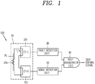
- a high-speed fault current detection circuit according to a first preferred embodiment of the present disclosure comprises a primary current transformer 10a, a pair of secondary current transformers 10b, 10c, a fault detection circuit section 20, a surge detection circuit section 30 and a trip determination circuit section 40.
- the primary current transformer 10a may detect a current flowing through a power circuit (PL) in a grid and primarily detect and output a current detection signal (i).
- the pair of secondary current transformers 10b, 10c are connected to the fault detection circuit section 20 and surge detection circuit section 30, respectively, through output terminals thereof to convert the current detection signal provided by the primary current transformer 10a into secondary conversion signals, respectively, with a small current so as to provide them to the fault detection circuit section 20 and surge detection circuit section 30, respectively.
- the pair of secondary current transformers 10b, 10c may be referred to as a secondary current transformer-1 10b and a secondary current transformer-2 10c, respectively.
- the fault detection circuit section 20 is connected to an output terminal of either one of the pair of secondary current transformers 10b, 10c, namely, the secondary current transformer-1 10b, to determine that a fault current occurs on the power circuit by comparing a current value represented by a secondary conversion signal outputted from the secondary current transformer-1 10b with a predetermined reference current when the current value is equal to or larger than a value of the predetermined reference current, and output a signal with a logical value "1" (one) as a fault detection signal when determined that a fault current has occurred.
- the value of the predetermined reference current may be predetermined as a current value in proportion to a rated current value of a circuit breaker or fault current limiter connected to the high-speed fault current detection circuit.
- the surge detection circuit section 30 is connected to an output terminal of the other one of the pair of secondary current transformers 10b, 10c, namely, the secondary current transformer-2 10c, to determine that a surge current occurs on the power circuit by comparing a current value represented by a secondary conversion signal outputted from the secondary current transformer-2 10c with a predetermined reference current when the current value is equal to or larger than a predetermined reference current value, and output a signal with a logical value "1" as a surge detection signal when determined that a surge current has occurred.
- the predetermined reference current value may be predetermined as a current value of signal that can be recognized as a predetermined typical surge signal.
- the trip determination circuit section 40 is connected to an output terminals of the fault detection circuit section 20 and surge detection circuit section 30 to receive the fault detection signal and the surge detection signal to generate a trip control signal when at least either one of the fault detection signal and the surge detection signal is received.
- the trip determination circuit section 40 may be configured with a logical OR circuit or logical AND circuit.
- a high-speed fault current detection circuit comprises a primary current transformer 10a, a pair of secondary current transformers 10b, 10c, a first amplifier circuit section 51, a first differentiator 61, a second amplifier circuit section 52, a second differentiator 62, a fault detection circuit section 20, a surge detection circuit section 30 and a trip determination circuit section 40.
- a high-speed fault current detection circuit according to a second preferred embodiment of the present disclosure further comprises a first amplifier circuit section 51, a first differentiator 61, a second amplifier circuit section 52 and a second differentiator 62 as a configuration difference from the foregoing high-speed fault current detection circuit according to a first preferred embodiment of the present disclosure. Accordingly, only different configuring elements will be described to avoid the redundant description thereof.
- the first amplifier circuit section 51 is connected between an output terminal of the secondary current transformer-1 10b of the pair of secondary current transformers and the fault detection circuit section 20 to amplify a secondary conversion signal outputted from the secondary current transformer-1 10b and output the amplified secondary conversion signal to the fault detection circuit section 20.
- the first differentiator 61 is connected between an output terminal of the secondary current transformer-1 10b of the pair of secondary current transformers and the fault detection circuit section 20 to differentiate a secondary conversion signal outputted from the secondary current transformer-1 10b and output a change gradient of the secondary conversion signal to the fault detection circuit section 20.
- the second amplifier circuit section 52 is connected between an output terminal of the secondary current transformer-2 10c of the pair of secondary current transformers and the surge detection circuit section 30 to amplify a secondary conversion signal outputted from the secondary current transformer-2 10c and output the amplified secondary conversion signal to the surge detection circuit section 30.
- the second differentiator 62 is connected between an output terminal of the secondary current transformer-2 10c of the pair of secondary current transformers and the surge detection circuit section 30 to differentiate a secondary conversion signal outputted from secondary current transformer-2 10c of the pair of secondary current transformers and output a change gradient of the secondary conversion signal to the surge detection circuit section 30.
- a high-speed fault current detection circuit comprises a primary current transformer 10a, a pair of secondary current transformers 10b, 10c, a first amplifier circuit section 51, a first differentiator 61, a third amplifier circuit section 53, a second amplifier circuit section 52, a second differentiator 62, a fourth amplifier circuit section 54, a fault detection circuit section 20, a surge detection circuit section 30 and a trip determination circuit section 40.
- a high-speed fault current detection circuit according to a third preferred embodiment of the present disclosure further comprises a third amplifier circuit section 53 and a fourth amplifier circuit section 54 as a configuration difference from the foregoing high-speed fault current detection circuit according to a second preferred embodiment of the present disclosure. Accordingly, only constituent elements different from the second embodiment will be described to avoid the redundant description thereof.
- the third amplifier circuit section 53 is connected to an output terminal of the first differentiator 61 to amplify and output a change gradient of the secondary conversion signal outputted from the first differentiator 61.
- the fourth amplifier circuit section 54 is connected between an output terminal of the second differentiator 62 and the surge detection circuit section 30 to amplify and output a change gradient of the secondary conversion signal outputted from the second differentiator 62.
- the fault detection circuit section 20 may comprise a first comparator 21 and a second comparator 22.
- the first comparator 21 is connected to an output terminal of the first amplifier circuit section 51 to compare a current value represented by the amplified secondary conversion signal from the first amplifier circuit section 51 with a predetermined first reference value so as to output a first fault detection signal when the current value represented by the amplified secondary conversion signal is no less than the first reference value, namely, equal to or larger than the first reference value.
- the first fault detection signal may be configured with a signal indicating a logical value "1".
- the second comparator 22 is connected to an output terminal of the third amplifier circuit section 53 to compare an amplification value of the change gradient from the third amplifier circuit section 53 with a predetermined second reference value so as to output a second fault detection signal when the change gradient from the second amplifier circuit section is no less than the second reference value, namely, when the change gradient from the second amplifier circuit section is equal to or larger than the second reference value.
- the second fault detection signal may be configured with a signal indicating a logical value "1".
- a configuration in which the fault detection circuit section 20 comprises the first comparator 21 and second comparator 22 has the same configuration as the fault detection circuit section 20 according to the foregoing first embodiment and second embodiment, and the redundant description thereof will be omitted.
- the surge detection circuit section 30 may comprise a third comparator 31 and a fourth comparator 32.
- the third comparator 31 is connected to an output terminal of the second amplifier circuit section 52 to compare a current value represented by the amplified secondary conversion signal from the second amplifier circuit section 52 with a predetermined third reference value so as to output a first surge detection signal when the current value represented by the amplified secondary conversion signal from the second amplifier circuit section 52 is no less than the third reference value, namely, when the current value represented by the amplified secondary conversion signal from the second amplifier circuit section 52 is equal to or larger than the third reference value.
- the first surge detection signal may be configured with a signal indicating a logical value "1".
- the fourth comparator 32 is connected to an output terminal of the fourth amplifier circuit section 54 to compare an amplification value of the change gradient from the fourth amplifier circuit section 54 with a predetermined fourth reference value so as to output a second surge detection signal when the amplification value of the change gradient from the fourth amplifier circuit section 54 is no less than the fourth reference value, namely, equal to or larger than the fourth reference value.
- the second surge detection signal may be configured with a signal indicating a logical value "1".
- the surge detection circuit section 30 comprises the third comparator 31 and fourth comparator 32 has the same configuration as the surge detection circuit section 30 according to the foregoing first embodiment and second embodiment, and the redundant description thereof will be omitted.
- an amplification ratio of the first amplifier circuit section 51 is a first amplification ratio
- an amplification ratio of the second amplifier circuit section 52 is a second amplification ratio
- an amplification ratio of the third amplifier circuit section 53 is a third amplification ratio
- an amplification ratio of the fourth amplifier circuit section 54 is a fourth amplification ratio
- the trip determination unit 40 is connected to an output terminal of the fault detection circuit section 20 and the surge detection circuit section 30 to receive the first fault detection signal, second fault detection signal, first surge detection signal and second surge detection signal, and when at least any one of the first fault detection signal, second fault detection signal, first surge detection signal and second surge detection signal is received, the trip determination circuit section 40 generates and outputs a trip control signal.
- the trip determination circuit section 40 may be configured with a logical OR circuit or logical AND circuit section.
- the configuration and operation of the trip determination circuit section 40 according to the foregoing first embodiment and second embodiment may be configure to have the same configuration and operation of the trip determination circuit section 40 in a high-speed fault current detection circuit according to the foregoing third embodiment.
- the primary current transformer 10a detects a current flowing through an electric power circuit (PL) in a grid and output a current detection signal (i).
- the current detection signal (i) primarily detected and outputted by the primary current transformer 10a has a large value, and thus is not appropriate to a processing signal level of a digital circuit section such as a comparator, a differentiator circuit, a logic circuit and the like, and a pair of secondary current transformers 10b, 10c are connected to the fault detection circuit section 20 and surge detection circuit section 30, respectively, through an output terminal thereof to convert the current detection signal provided by the primary current transformer 10a into secondary conversion signals, respectively, with a small current and provide them to the fault detection circuit section 20 and surge detection circuit section 30, respectively.
- a digital circuit section such as a comparator, a differentiator circuit, a logic circuit and the like
- the fault detection circuit section 20 determines that a fault current occurs on the electric power circuit by comparing a current value represented by a secondary conversion signal outputted from the secondary current transformer-1 10b with a predetermined reference current value when the current value represented by the secondary conversion signal is equal to or larger than the predetermined reference current value, and outputs a signal with a logical value "1 " as a fault detection signal when determined that the fault current has occurred.
- the surge detection circuit section 30 is connected to an output terminal of the other one of the pair of secondary current transformers 10b, 10c, namely, the secondary current transformer-2 10c to determine that a surge current occurs on the electric power circuit by comparing a current value represented by a secondary conversion signal outputted from the secondary current transformer-2 10c with a predetermined reference current value when the current value is larger than the predetermined reference current value, and outputs a signal with a logical value "1" as a surge detection signal when determined that the surge current has occurred.
- the trip determination circuit section 40 When the trip determination circuit section 40 is configured with a logical OR circuit, the trip determination circuit section 40 generates and outputs a trip control signal when at least either one of the fault detection signal and the surge detection signal is received as a signal with a logical value "1".
- the trip determination circuit section 40 When the trip determination circuit section 40 is configured with a logical AND circuit, the trip determination circuit section 40 generates and outputs a trip control signal only when a signal with a logical value "1" is received as the fault detection signal and the surge detection signal at the same time.
- the trip control signal generated and output in this manner may be provided to a circuit breaker (not shown) to perform a trip operation or provided to a fault current limiter (not shown) to trip or limit a fault current and/or surge current occurred on the electric power circuit (PL) in the grid by allowing the relevant circuit breaker to perform a trip (automatic circuit break) operation in response to this or the fault current limiter to perform a fault current limiting operation in response to this, thereby protecting a circuit connected as a next stage of the relevant circuit breaker or fault current limiter and a load device connected thereto.
- a circuit breaker not shown
- a fault current limiter not shown
- the primary current transformer 10a detects a current flowing through an electric power circuit (PL) in a grid and output a current detection signal (i).
- the pair of secondary current transformers 10b, 10c convert the current detection signal provided by the primary current transformer 10a into secondary conversion signals, respectively, with a small current such that the secondary current transformer-1 10b provides a secondary conversion signal to the first amplifier circuit section 51 and first differentiator 61, and the secondary current transformer-2 10c provides a secondary conversion signal to the second amplifier circuit section 52 and second differentiator 62.
- the first amplifier circuit section 51 amplifies a secondary conversion signal outputted from the secondary current transformer-1 10b to output the amplified secondary conversion signal to the fault detection circuit section 20.
- the first differentiator 61 differentiates a secondary conversion signal outputted from the secondary current transformer-1 10b to output a change gradient of the secondary conversion signal to the fault detection circuit section 20.
- the second amplifier circuit section 52 amplifies and output the secondary conversion signal outputted from the secondary current transformer-2 10c to the surge detection circuit section 30.
- the second differentiator 62 differentiate the secondary conversion signal outputted from the secondary current transformer-2 10c to output a change gradient of the secondary conversion signal to the surge detection circuit section 30.
- the first comparator 21 included in the fault detection circuit section 20 compares a current value represented by the amplified secondary conversion signal from the first amplifier circuit section 51 with a predetermined first reference value to output a first fault detection signal as a logical value "1" when the current value represented by the amplified secondary conversion signal is no less than the first reference value, namely, equal to or larger than the first reference value.
- the second comparator 22 included in the fault detection circuit section 20 compares the change gradient value from the first differentiator 61 with a predetermined second reference value to output a second fault detection signal when the change gradient value from the first differentiator 61 is no less than the second reference value, namely, when a valued represented by the change gradient from the first differentiator 61 is equal to or larger than the second reference.
- the second fault detection signal may be configured with a signal indicating a logical value "1".
- the third comparator 31 compares a current value represented by the amplified secondary conversion signal from the second amplifier circuit section 52 with a predetermined third reference value to output a first surge detection signal as a logical value "1" when a current value represented by the amplified secondary conversion signal from the second amplifier circuit section 52 is no less than the third reference value, namely, when the current value represented by the amplified secondary conversion signal from the second amplifier circuit section 52 is equal to or larger than the third reference value.
- the fourth comparator 32 compares a value of the change gradient from the second differentiator 62 with a predetermined fourth reference value to output a second surge detection signal when the value of the change gradient from the second differentiator 62 is no less than the fourth reference value, namely, equal to or larger than the fourth reference value.
- the second surge detection signal may be configured with a signal indicating a logical value "1".
- the trip determination circuit section 40 when the trip determination circuit section 40 is configured with a logical OR circuit, the trip determination circuit section 40 generates and outputs a trip control signal when at least any one of the first fault detection signal, the second fault detection signal, the first surge detection signal and the second surge detection signal is received as a signal with a logical value "1".
- the trip determination circuit section 40 When the trip determination circuit section 40 is configured with a logical AND circuit, the trip determination circuit section 40 generates and outputs a trip control signal when the first fault detection signal, the second fault detection signal, the first surge detection signal and the second surge detection signal are all received at the same time as a signal with a logical value "1".
- the use of the trip control signal is similar to the operation of the foregoing first embodiment, and thus provided to a circuit breaker (not shown) to perform a trip operation or provided to the fault current limiter (not shown).
- the primary current transformer 10a detects a current flowing through an electric power circuit (PL) in a grid to primarily detect and output a current detection signal (i).
- a pair of secondary current transformers 10b, 10c convert the current detection signal provided by the primary current transformer 10a into secondary conversion signals, respectively, with a small current such that the secondary current transformer-1 10b provides a secondary conversion signal to the first amplifier circuit section 51 and first differentiator 61, and the secondary current transformer-2 10c provides a secondary conversion signal to the second amplifier circuit section 52 and second differentiator 62.
- the first amplifier circuit section 51 amplifies the secondary conversion signal outputted from the secondary current transformer-1 10b to output the amplified secondary conversion signal to the fault detection circuit section 20.
- the first differentiator 61 differentiates the secondary conversion signal outputted from the secondary current transformer-1 10b to output a change gradient of the secondary conversion signal to the third amplifier circuit section 53.
- the second amplifier circuit section 52 amplifies and output the secondary conversion signal outputted from the secondary current transformer-2 10c to the surge detection circuit section 30.
- the second differentiator 62 differentiate a secondary conversion signal outputted from the secondary current transformer-2 10c to output a change gradient of the secondary conversion signal to the fourth amplifier circuit section 54.
- the fourth amplifier circuit section 54 amplifies and outputs a signal represented by a change gradient from the second differentiator 62 to the surge detection circuit section 30.
- the first comparator 21 included in the fault detection circuit section 20 compares a current value represented by the amplified secondary conversion signal from the first amplifier circuit section 51 with a predetermined first reference value to output a first fault detection signal as a logical value "1" when the current value represented by the amplified secondary conversion signal is no less than the first reference value, namely, equal to or larger than the first reference value.
- the second comparator 22 included in the fault detection circuit section 20 compares an amplification value of the change gradient value from the third amplifier circuit section 53 with a predetermined second reference value to output a second fault detection signal when the amplification value of the change gradient value from the first differentiator 61 is no less than the second reference value, namely, when the amplification value of the change gradient from the first differentiator 61 is equal to or larger than the second reference.
- the second fault detection signal may be configured with a signal indicating a logical value "1".
- the third comparator 31 compares a current value represented by the amplified secondary conversion signal from the second amplifier circuit section 52 with a predetermined third reference value to output a first surge detection signal as a logical value "1" when a current value represented by the amplified secondary conversion signal from the second amplifier circuit section 52 is no less than the third reference value, namely, when the current value represented by the amplified secondary conversion signal from the second amplifier circuit section 52 is equal to or larger than the third reference value.
- the fourth comparator 32 compares an amplification value of the change gradient from the fourth amplifier circuit section 54 with a predetermined fourth reference value to output a second surge detection signal when the amplification value of the change gradient from the second differentiator 62 is no less than the fourth reference value, namely, equal to or larger than the fourth reference value.
- the second surge detection signal may be configured with a signal indicating a logical value "1".
- the trip determination circuit section 40 when the trip determination circuit section 40 is configured with a logical OR circuit, the trip determination circuit section 40 generates and outputs a trip control signal when at least any one of the first fault detection signal, the second fault detection signal, the first surge detection signal and the second surge detection signal is received as a signal with a logical value "1".
- a high-speed fault current detection circuit outputs a trip control signal, thereby opening the electric power circuit through a circuit breaker or limiting a current through the fault current limiter.
- the trip determination circuit section 40 When the trip determination circuit section 40 is configured with a logical AND circuit, the trip determination circuit section 40 generates and outputs a trip control signal when the first fault detection signal, the second fault detection signal, the first surge detection signal and the second surge detection signal are all received at the same time as a signal with a logical value "1".
- a high-speed fault current detection circuit outputs a trip control signal, thereby opening a circuit through a circuit breaker or limiting a current through the fault current limiter.
- a high-speed fault current detection circuit may be configured with a pair of (two) secondary current transformers, and those secondary current transformers, respectively, are configured to connect to the fault detection circuit section for detecting a fault current exceeding a rated current of the circuit breaker and the surge detection circuit section for detecting a surge current in a separate manner so as to independently detect a fault current and a surge current having largely different current sizes thereof, thereby providing an effect of enhancing detection accuracy.
- a high-speed fault current detection circuit may comprise a first amplifier circuit section configured to amplify a secondary conversion signal outputted by either one of the one pair of secondary current transformers and output the amplified secondary conversion signal to the fault detection circuit section, a first differentiator configured to differentiate a secondary conversion signal outputted by either one of the one pair of secondary current transformers and output a change gradient of the secondary conversion signal to the fault detection circuit section, a second amplifier circuit section configured to amplify a secondary conversion signal outputted by the other one of the one pair of secondary current transformers and output the amplified secondary conversion signal to the surge detection circuit section, and a second differentiator configured to output a change gradient of the secondary conversion signal outputted by the other one of the one pair of secondary current transformers to the surge detection circuit section, thereby obtaining an effect of allowing the fault detection circuit section to receive the amplified secondary conversion signal which is a failure current detection signal from the relevant secondary current transformer as well as receiving its change gradient, and allowing the surge detection circuit section to receive the ampl
- the fault detection circuit section may comprise a first comparator configured to compare a current value represented by the amplified secondary conversion signal from the first amplifier circuit section with a predetermined first reference value, and a second comparator configured to compare the change gradient of the secondary conversion signal with a predetermined second reference value, thereby obtaining an effect of determining whether or not a fault current exceeding a reference current has occurred as well as determining whether the change gradient exceeds a reference value.
- the surge detection circuit section may comprise a third comparator configured to compare a current value represented by the amplified secondary conversion signal from the second amplifier circuit section with a predetermined third reference value, and a fourth comparator configured to compare a change gradient of the secondary conversion signal outputted by the second differentiator with a predetermined fourth reference value, thereby obtaining an effect of determining whether or not a surge current exceeding a reference current has occurred as well as determining whether the change gradient of the surge current exceeds a reference value.
- an amplification ratio of the first amplifier circuit section is a first amplification ratio
- an amplification ratio of the second amplifier circuit section is a second amplification ratio
- an amplification ratio of the third amplifier circuit section is a third amplification ratio
- an amplification ratio of the fourth amplifier circuit section is a fourth amplification ratio
- an amplification ratio of the amplifier unit configured to amplify a surge current or a change gradient of the surge current with regard to the surge current having a larger current value compared to the fault current may be configured to be different (smaller) than that of the amplification unit configured to amplify a detection fault current having a value smaller than that or a change gradient of the detection fault current, thereby providing an effect of enhancing the detection reliability of the fault current as well as the surge current.
- the trip determination unit may be configured with a logical OR circuit to generate a trip control signal when a fault current is detected or a change gradient of the fault current is abrupt or a surge current is detected or a change gradient of the surge current is abrupt so as to perform a circuit breaking or fault current limiting operation in the relevant case, thereby obtaining an effect of protecting a circuit connected as next stage thereof and a load device connected to the circuit from the fault current or surge current.
- the trip determination unit may be configured with a logical AND circuit to generate a trip control signal when a fault current is detected and a change gradient thereof is abrupt and a surge current is also detected and a change gradient thereof is also abrupt so as to perform a circuit breaking or fault current limiting operation with respect to a large detection current indicating an abrupt change gradient, thereby obtaining an effect of preventing an error operation of the circuit breaker or fault current limiter.
Description
- The present disclosure relates to a fault current limiter which is one of electric power receiving and distributing equipment, and more particularly, to a high-speed fault current detection circuit for the fault current limiter.
- As a protection device for protecting an electric circuit from a fault current such as an overcurrent or short-circuit current, a fault current limiter (can be abbreviated as "FCL"), which is one of electric power receiving and distributing equipment, is an apparatus for reducing a fault current below an appropriate value within a short period of time to enhance the mechanical/thermal stress prevention of an electric power device and grid reliability when a large fault current occurs in a grid.
- For an example of conventional technologies for high-speed fault current detection circuits as such fault current limiters, the following patent literature disclosed by the applicant of the present disclosure is descried below for reference.
- (Patent Literature 1) KR10-2014-0055129 A
- A high-speed fault current detection circuit in the related art according to the patent document has a configuration in which a detection signal detected through one common secondary current transformer is shared for a fault currents and surge currents. In terms of a current signal received in the high-speed fault current detection circuit, the size of a surge current is significantly larger than that of a fault current, and thus has a big difference therebetween, and when it is detected with a common detection device and amplified with a common amplifier circuit section, the detection accuracy of a fault current having a size smaller than that of a surge current is reduced, thus causing a problem in the reliability of the high-speed fault current detection circuit as a whole.
-
US 3,786,311 which is regarded as closest prior art discloses a circuit breaker including separable contacts, an operating means for opening and closing the contacts and a trip coil responsive to a static control circuit for tripping the circuit breaker when instantaneous power in one of the phases of a three phase alternating current circuit exceeds adjustable predetermined levels for adjustable predetermined times as well as ground faults. A separate non-saturated iron core current transformer detects the current in each of the phases independently and powers independent cascaded current transformers having outputs of the same polarity connected to form OR circuits and provide a voltage signal correlated with the instantaneous current in a single one of the protected lines with the highest signal back biasing the others. This signal is amplified and delivered to a plurality of independent solid state adjustable time delay circuits for instantaneous time delay, short time delay and long time delay actuation of the trip coil dependent upon the extent to which the current levels in the protected line providing the signal exceeds a predetermined level of line current. Ground fault protection is also provided. -
EP 2 728 691 A1 - Accordingly, the present disclosure is provided to solve the problem in the related art, and an aspect of the present disclosure is to provide a high-speed fault current detection circuit capable of enhancing the detection accuracy of a fault current exceeding a rated current of a circuit breaker while at the same time allowing the accurate detection of a surge current to enhance reliability.
- The foregoing object of the present disclosure may be accomplished by providing a high-speed fault current detection circuit according to
claim 1. Said circuit comprises inter alia: - a primary current transformer configured to detect a current flowing through an electric power circuit in a grid to output a current detection signal;
- a pair of secondary current transformers connected to the primary current transformer to convert and provide the current detection signal provided by the primary current transformer into secondary conversion signals, respectively, with a small current;
- a fault detection circuit section connected to any one output terminal of the one pair of secondary current transformers to determine whether or not a fault current occurs on the electric power circuit by comparing a current value
- represented by a secondary conversion signal outputted by either one of the one pair of secondary current transformers with a predetermined reference current value, and output a fault detection signal when determined that the fault current has occurred;
- a surge detection circuit section connected to the other output terminal of the one pair of secondary current transformers to determine whether or not a surge current occurs on the electric power circuit by comparing a current value represented by a secondary conversion signal outputted by the other one of the one pair of secondary current transformers with a predetermined reference current value, and output a surge detection signal when determined that the surge current has occurred; and
- a trip determination unit connected to output terminals of the fault detection circuit section and the surge detection circuit section to receive the fault detection signal and the surge detection signal, and generates a trip control signal when at least either one of the fault detection signal and the surge detection signal is received.
- The high-speed fault current detection circuit according to present disclosure, further comprises:
- a first amplifier circuit section connected between either one output terminal of the one pair of secondary current transformers and the fault detection circuit section to amplify a secondary conversion signal outputted by either one of the one pair of secondary current transformers and output the amplified secondary conversion signal to the fault detection circuit section;
- a first differentiator connected between either one output terminal of the one pair of secondary current transformers and the fault detection circuit section to differentiate a secondary conversion signal outputted by either one of the one pair of secondary current transformers and output a change gradient of the secondary conversion signal to the fault detection circuit section;
- a second amplifier circuit section connected between the other output terminal of the one pair of secondary current transformers and the surge detection circuit section to amplify a secondary conversion signal outputted by the other one of the one pair of secondary current transformers and output the amplified secondary conversion signal to the surge detection circuit section; and
- a second differentiator connected between the other output terminal of the one pair of secondary current transformers and the surge detection circuit section to differentiate a secondary conversion signal outputted by the other one of the one pair of secondary current transformers and output a change gradient of the secondary conversion signal to the surge detection circuit section.
- According to the present disclosure, the fault detection circuit section comprises:
- a first comparator connected to an output terminal of the first amplifier circuit section to compare a current value represented by the amplified secondary conversion signal from the first amplifier circuit section with a predetermined first reference value; and
- a second comparator configured to compare the change gradient with a predetermined second reference value.
- According to the present disclosure, the surge detection circuit section comprises:
- a third comparator connected to an output terminal of the second amplifier circuit section to compare a current value represented by the amplified secondary conversion signal from the second amplifier circuit section with a predetermined third reference value; and
- a fourth comparator configured to compare a change gradient of the secondary conversion signal outputted by the second differentiator with a predetermined fourth reference value.
- According to the present disclosure, the high-speed fault current detection circuit according to present disclosure further comprises:
- a first amplifier circuit section connected to either one output terminal of the one pair of secondary current transformers to amplify a secondary conversion signal outputted by either one of the one pair of secondary current transformers and output the amplified secondary conversion signal;
- a first differentiator connected to either one output terminal of the one pair of secondary current transformers to differentiate a secondary conversion signal outputted by either one of the one pair of secondary current transformers and output a change gradient of the secondary conversion signal;
- a third amplifier circuit section connected to an output terminal of the first differentiator to amplify and output a change gradient of the secondary conversion signal outputted by the first differentiator;
- a second amplifier circuit section connected to the other output terminal of the one pair of secondary current transformers to amplify a secondary conversion signal outputted by the other one of the one pair of secondary current transformers and output the amplified secondary conversion signal;
- a second differentiator connected to the other output terminal of the one pair of secondary current transformers to differentiate a secondary conversion signal outputted by the other one of the one pair of secondary current transformers and output a change gradient of the secondary conversion signal; and
- a fourth amplifier circuit section connected to an output terminal of the second differentiator to amplify a change gradient of the secondary conversion signal outputted by the second differentiator,
- wherein the fault detection circuit section comprises:
- a first comparator connected to an output terminal of the first amplifier circuit section to compare a current value represented by the amplified secondary conversion signal from the first amplifier circuit section with a predetermined first reference value so as to output a first fault detection signal when the current value represented by the amplified secondary conversion signal is no less than the first reference value; and
- a second comparator connected to an output terminal of the third amplifier circuit section to compare an amplification value of the change gradient from the third amplifier circuit section with a predetermined second reference value so as to output a second fault detection signal when the change gradient from the third amplifier circuit section is no less than the second reference value, and
- the surge detection circuit section comprises:
- a third comparator connected to an output terminal of the second amplifier circuit section to compare a current value represented by the amplified secondary conversion signal from the second amplifier circuit section with a predetermined third reference value so as to output a first surge detection signal when the current value represented by the amplified secondary conversion signal from the second amplifier circuit section is no less than the third reference value; and
- a fourth comparator connected to an output terminal of the fourth amplifier circuit section to compare an amplification value of the change gradient from the fourth amplifier circuit section with a predetermined fourth reference value so as to output a second surge detection signal when the amplification value of the change gradient from the fourth amplifier circuit section is no less than the fourth reference value, and
- the trip determination unit is connected to output terminals of the fault detection circuit section and the surge detection circuit section to receive the first fault detection signal, second fault detection signal, first surge detection signal and second surge detection signal, and configured to generate a trip control signal when at least any one of the first fault detection signal, second fault detection signal, first surge detection signal and second surge detection signal is received.
- According to the present disclosure, when an amplification ratio of the first amplifier circuit section is a first amplification ratio, and an amplification ratio of the second amplifier circuit section is a second amplification ratio, and an amplification ratio of the third amplifier circuit section is a third amplification ratio, and an amplification ratio of the fourth amplifier circuit section is a fourth amplification ratio, the first amplification ratio > the second amplification ratio, and the third amplification ratio > the fourth amplification ratio.
- According to still another aspect of the present disclosure, the trip determination unit is configured with a logical OR circuit.
- According to still another aspect of the present disclosure, the trip determination unit is configured with a logical AND circuit.
- The accompanying drawings, which are included to provide a further understanding of the invention and are incorporated in and constitute a part of this specification, illustrate embodiments of the invention and together with the description serve to explain the principles of the invention.
- In the drawings:
-
FIG. 1 is a block diagram illustrating the configuration of a high-speed fault current detection circuit according to an embodiment of the present disclosure; -
FIG. 2 is a block diagram illustrating the configuration of a high-speed fault current detection circuit according to another embodiment of the present disclosure; and -
FIG. 3 is a block diagram illustrating the configuration of a high-speed fault current detection circuit according to still another embodiment of the present disclosure. - The objective of the present invention, as well as the configuration and working effect thereof to accomplish the foregoing objective will be more clearly understood by the following description for the preferred embodiments of present disclosure with reference to the accompanying drawings.
- First, the configuration of a high-speed fault current detection circuit according to a preferred embodiment of the present disclosure will be described with reference to
FIG. 1 . - Referring to
FIG. 1 , a high-speed fault current detection circuit according to a first preferred embodiment of the present disclosure comprises a primarycurrent transformer 10a, a pair ofsecondary current transformers detection circuit section 20, a surgedetection circuit section 30 and a tripdetermination circuit section 40. - As a circuit section included in a
current detection unit 10, the primarycurrent transformer 10a may detect a current flowing through a power circuit (PL) in a grid and primarily detect and output a current detection signal (i). - The pair of
secondary current transformers detection circuit section 20 and surgedetection circuit section 30, respectively, through output terminals thereof to convert the current detection signal provided by the primarycurrent transformer 10a into secondary conversion signals, respectively, with a small current so as to provide them to the faultdetection circuit section 20 and surgedetection circuit section 30, respectively. Here, the pair of secondarycurrent transformers - The fault
detection circuit section 20 is connected to an output terminal of either one of the pair of secondarycurrent transformers - The surge
detection circuit section 30 is connected to an output terminal of the other one of the pair of secondarycurrent transformers - The trip
determination circuit section 40 is connected to an output terminals of the faultdetection circuit section 20 and surgedetection circuit section 30 to receive the fault detection signal and the surge detection signal to generate a trip control signal when at least either one of the fault detection signal and the surge detection signal is received. To this end, the tripdetermination circuit section 40 may be configured with a logical OR circuit or logical AND circuit. - On the other hand, the configuration of a high-speed fault current detection circuit according to a second preferred embodiment of the present disclosure will be described with reference to
FIG. 2 . - As illustrated in
FIG. 2 , a high-speed fault current detection circuit according to a second preferred embodiment of the present disclosure comprises a primarycurrent transformer 10a, a pair of secondarycurrent transformers amplifier circuit section 51, afirst differentiator 61, a secondamplifier circuit section 52, asecond differentiator 62, a faultdetection circuit section 20, a surgedetection circuit section 30 and a tripdetermination circuit section 40. - As illustrated in
FIG. 2 , a high-speed fault current detection circuit according to a second preferred embodiment of the present disclosure further comprises a firstamplifier circuit section 51, afirst differentiator 61, a secondamplifier circuit section 52 and asecond differentiator 62 as a configuration difference from the foregoing high-speed fault current detection circuit according to a first preferred embodiment of the present disclosure. Accordingly, only different configuring elements will be described to avoid the redundant description thereof. - The first
amplifier circuit section 51 is connected between an output terminal of the secondary current transformer-1 10b of the pair of secondary current transformers and the faultdetection circuit section 20 to amplify a secondary conversion signal outputted from the secondary current transformer-1 10b and output the amplified secondary conversion signal to the faultdetection circuit section 20. - The
first differentiator 61 is connected between an output terminal of the secondary current transformer-1 10b of the pair of secondary current transformers and the faultdetection circuit section 20 to differentiate a secondary conversion signal outputted from the secondary current transformer-1 10b and output a change gradient of the secondary conversion signal to the faultdetection circuit section 20. - The second
amplifier circuit section 52 is connected between an output terminal of the secondary current transformer-2 10c of the pair of secondary current transformers and the surgedetection circuit section 30 to amplify a secondary conversion signal outputted from the secondary current transformer-2 10c and output the amplified secondary conversion signal to the surgedetection circuit section 30. - The
second differentiator 62 is connected between an output terminal of the secondary current transformer-2 10c of the pair of secondary current transformers and the surgedetection circuit section 30 to differentiate a secondary conversion signal outputted from secondary current transformer-2 10c of the pair of secondary current transformers and output a change gradient of the secondary conversion signal to the surgedetection circuit section 30. - On the other hand, the configuration of a high-speed fault current detection circuit according to a third preferred embodiment of the present disclosure will be described with reference to
FIG. 3 . - As illustrated in
FIG. 3 , a high-speed fault current detection circuit according to a third preferred embodiment of the present disclosure comprises a primarycurrent transformer 10a, a pair of secondarycurrent transformers amplifier circuit section 51, afirst differentiator 61, a thirdamplifier circuit section 53, a secondamplifier circuit section 52, asecond differentiator 62, a fourthamplifier circuit section 54, a faultdetection circuit section 20, a surgedetection circuit section 30 and a tripdetermination circuit section 40. - As illustrated in
FIG. 3 , a high-speed fault current detection circuit according to a third preferred embodiment of the present disclosure further comprises a thirdamplifier circuit section 53 and a fourthamplifier circuit section 54 as a configuration difference from the foregoing high-speed fault current detection circuit according to a second preferred embodiment of the present disclosure. Accordingly, only constituent elements different from the second embodiment will be described to avoid the redundant description thereof. - The third
amplifier circuit section 53 is connected to an output terminal of thefirst differentiator 61 to amplify and output a change gradient of the secondary conversion signal outputted from thefirst differentiator 61. - The fourth
amplifier circuit section 54 is connected between an output terminal of thesecond differentiator 62 and the surgedetection circuit section 30 to amplify and output a change gradient of the secondary conversion signal outputted from thesecond differentiator 62. - On the other hand, referring to
FIG. 3 , the faultdetection circuit section 20 may comprise afirst comparator 21 and asecond comparator 22. - The
first comparator 21 is connected to an output terminal of the firstamplifier circuit section 51 to compare a current value represented by the amplified secondary conversion signal from the firstamplifier circuit section 51 with a predetermined first reference value so as to output a first fault detection signal when the current value represented by the amplified secondary conversion signal is no less than the first reference value, namely, equal to or larger than the first reference value. Here, the first fault detection signal may be configured with a signal indicating a logical value "1". - The
second comparator 22 is connected to an output terminal of the thirdamplifier circuit section 53 to compare an amplification value of the change gradient from the thirdamplifier circuit section 53 with a predetermined second reference value so as to output a second fault detection signal when the change gradient from the second amplifier circuit section is no less than the second reference value, namely, when the change gradient from the second amplifier circuit section is equal to or larger than the second reference value. Here, the second fault detection signal may be configured with a signal indicating a logical value "1". - Here, a configuration in which the fault
detection circuit section 20 comprises thefirst comparator 21 andsecond comparator 22 has the same configuration as the faultdetection circuit section 20 according to the foregoing first embodiment and second embodiment, and the redundant description thereof will be omitted. - Moreover, referring to
FIG. 3 , the surgedetection circuit section 30 may comprise athird comparator 31 and afourth comparator 32. - The
third comparator 31 is connected to an output terminal of the secondamplifier circuit section 52 to compare a current value represented by the amplified secondary conversion signal from the secondamplifier circuit section 52 with a predetermined third reference value so as to output a first surge detection signal when the current value represented by the amplified secondary conversion signal from the secondamplifier circuit section 52 is no less than the third reference value, namely, when the current value represented by the amplified secondary conversion signal from the secondamplifier circuit section 52 is equal to or larger than the third reference value. Here, the first surge detection signal may be configured with a signal indicating a logical value "1". - The
fourth comparator 32 is connected to an output terminal of the fourthamplifier circuit section 54 to compare an amplification value of the change gradient from the fourthamplifier circuit section 54 with a predetermined fourth reference value so as to output a second surge detection signal when the amplification value of the change gradient from the fourthamplifier circuit section 54 is no less than the fourth reference value, namely, equal to or larger than the fourth reference value. Here, the second surge detection signal may be configured with a signal indicating a logical value "1". - Furthermore, a configuration in which the surge
detection circuit section 30 comprises thethird comparator 31 andfourth comparator 32 has the same configuration as the surgedetection circuit section 30 according to the foregoing first embodiment and second embodiment, and the redundant description thereof will be omitted. - According to a preferred aspect of the present disclosure, when an amplification ratio of the first
amplifier circuit section 51 is a first amplification ratio, and an amplification ratio of the secondamplifier circuit section 52 is a second amplification ratio, and an amplification ratio of the thirdamplifier circuit section 53 is a third amplification ratio, and an amplification ratio of the fourthamplifier circuit section 54 is a fourth amplification ratio, the first amplification ratio > the second amplification ratio, and the third amplification ratio > the fourth amplification ratio. - Furthermore, as illustrated in
FIG. 3 , in a high-speed fault current detection circuit according to a third embodiment of the present disclosure, thetrip determination unit 40 is connected to an output terminal of the faultdetection circuit section 20 and the surgedetection circuit section 30 to receive the first fault detection signal, second fault detection signal, first surge detection signal and second surge detection signal, and when at least any one of the first fault detection signal, second fault detection signal, first surge detection signal and second surge detection signal is received, the tripdetermination circuit section 40 generates and outputs a trip control signal. To this end, the tripdetermination circuit section 40 may be configured with a logical OR circuit or logical AND circuit section. - The configuration and operation of the trip
determination circuit section 40 according to the foregoing first embodiment and second embodiment may be configure to have the same configuration and operation of the tripdetermination circuit section 40 in a high-speed fault current detection circuit according to the foregoing third embodiment. - The operation of a high-speed fault current detection circuit having the foregoing configuration according to a preferred embodiment of the present disclosure will be described below.
- First, the operation of a high-speed fault current detection circuit according to a first embodiment of the present disclosure will be described with reference to
FIG. 1 . - The primary
current transformer 10a detects a current flowing through an electric power circuit (PL) in a grid and output a current detection signal (i). - The current detection signal (i) primarily detected and outputted by the primary
current transformer 10a has a large value, and thus is not appropriate to a processing signal level of a digital circuit section such as a comparator, a differentiator circuit, a logic circuit and the like, and a pair of secondarycurrent transformers detection circuit section 20 and surgedetection circuit section 30, respectively, through an output terminal thereof to convert the current detection signal provided by the primarycurrent transformer 10a into secondary conversion signals, respectively, with a small current and provide them to the faultdetection circuit section 20 and surgedetection circuit section 30, respectively. - The fault
detection circuit section 20 determines that a fault current occurs on the electric power circuit by comparing a current value represented by a secondary conversion signal outputted from the secondary current transformer-1 10b with a predetermined reference current value when the current value represented by the secondary conversion signal is equal to or larger than the predetermined reference current value, and outputs a signal with a logical value "1 " as a fault detection signal when determined that the fault current has occurred. - The surge
detection circuit section 30 is connected to an output terminal of the other one of the pair of secondarycurrent transformers - When the trip
determination circuit section 40 is configured with a logical OR circuit, the tripdetermination circuit section 40 generates and outputs a trip control signal when at least either one of the fault detection signal and the surge detection signal is received as a signal with a logical value "1". - When the trip
determination circuit section 40 is configured with a logical AND circuit, the tripdetermination circuit section 40 generates and outputs a trip control signal only when a signal with a logical value "1" is received as the fault detection signal and the surge detection signal at the same time. - The trip control signal generated and output in this manner may be provided to a circuit breaker (not shown) to perform a trip operation or provided to a fault current limiter (not shown) to trip or limit a fault current and/or surge current occurred on the electric power circuit (PL) in the grid by allowing the relevant circuit breaker to perform a trip (automatic circuit break) operation in response to this or the fault current limiter to perform a fault current limiting operation in response to this, thereby protecting a circuit connected as a next stage of the relevant circuit breaker or fault current limiter and a load device connected thereto.
- Next, the operation of a high-speed fault current detection circuit according to a second embodiment of the present disclosure will be described with reference to
FIG. 2 . - The primary
current transformer 10a detects a current flowing through an electric power circuit (PL) in a grid and output a current detection signal (i). - Then, the pair of secondary
current transformers current transformer 10a into secondary conversion signals, respectively, with a small current such that the secondary current transformer-1 10b provides a secondary conversion signal to the firstamplifier circuit section 51 andfirst differentiator 61, and the secondary current transformer-2 10c provides a secondary conversion signal to the secondamplifier circuit section 52 andsecond differentiator 62. - As a result, the first
amplifier circuit section 51 amplifies a secondary conversion signal outputted from the secondary current transformer-1 10b to output the amplified secondary conversion signal to the faultdetection circuit section 20. - The
first differentiator 61 differentiates a secondary conversion signal outputted from the secondary current transformer-1 10b to output a change gradient of the secondary conversion signal to the faultdetection circuit section 20. - The second
amplifier circuit section 52 amplifies and output the secondary conversion signal outputted from the secondary current transformer-2 10c to the surgedetection circuit section 30. - The
second differentiator 62 differentiate the secondary conversion signal outputted from the secondary current transformer-2 10c to output a change gradient of the secondary conversion signal to the surgedetection circuit section 30. - Then, the
first comparator 21 included in the faultdetection circuit section 20 compares a current value represented by the amplified secondary conversion signal from the firstamplifier circuit section 51 with a predetermined first reference value to output a first fault detection signal as a logical value "1" when the current value represented by the amplified secondary conversion signal is no less than the first reference value, namely, equal to or larger than the first reference value. - Furthermore, the
second comparator 22 included in the faultdetection circuit section 20 compares the change gradient value from thefirst differentiator 61 with a predetermined second reference value to output a second fault detection signal when the change gradient value from thefirst differentiator 61 is no less than the second reference value, namely, when a valued represented by the change gradient from thefirst differentiator 61 is equal to or larger than the second reference. Here, the second fault detection signal may be configured with a signal indicating a logical value "1". - The
third comparator 31 compares a current value represented by the amplified secondary conversion signal from the secondamplifier circuit section 52 with a predetermined third reference value to output a first surge detection signal as a logical value "1" when a current value represented by the amplified secondary conversion signal from the secondamplifier circuit section 52 is no less than the third reference value, namely, when the current value represented by the amplified secondary conversion signal from the secondamplifier circuit section 52 is equal to or larger than the third reference value. - The
fourth comparator 32 compares a value of the change gradient from thesecond differentiator 62 with a predetermined fourth reference value to output a second surge detection signal when the value of the change gradient from thesecond differentiator 62 is no less than the fourth reference value, namely, equal to or larger than the fourth reference value. Here, the second surge detection signal may be configured with a signal indicating a logical value "1". - Then, when the trip
determination circuit section 40 is configured with a logical OR circuit, the tripdetermination circuit section 40 generates and outputs a trip control signal when at least any one of the first fault detection signal, the second fault detection signal, the first surge detection signal and the second surge detection signal is received as a signal with a logical value "1". - When the trip
determination circuit section 40 is configured with a logical AND circuit, the tripdetermination circuit section 40 generates and outputs a trip control signal when the first fault detection signal, the second fault detection signal, the first surge detection signal and the second surge detection signal are all received at the same time as a signal with a logical value "1". - Then, the use of the trip control signal is similar to the operation of the foregoing first embodiment, and thus provided to a circuit breaker (not shown) to perform a trip operation or provided to the fault current limiter (not shown).
- Next, the operation of a high-speed fault current detection circuit according to a third embodiment of the present disclosure will be described with reference to
FIG. 3 . - The primary
current transformer 10a detects a current flowing through an electric power circuit (PL) in a grid to primarily detect and output a current detection signal (i). - Then, a pair of secondary
current transformers current transformer 10a into secondary conversion signals, respectively, with a small current such that the secondary current transformer-1 10b provides a secondary conversion signal to the firstamplifier circuit section 51 andfirst differentiator 61, and the secondary current transformer-2 10c provides a secondary conversion signal to the secondamplifier circuit section 52 andsecond differentiator 62. - As a result, the first
amplifier circuit section 51 amplifies the secondary conversion signal outputted from the secondary current transformer-1 10b to output the amplified secondary conversion signal to the faultdetection circuit section 20. - The
first differentiator 61 differentiates the secondary conversion signal outputted from the secondary current transformer-1 10b to output a change gradient of the secondary conversion signal to the thirdamplifier circuit section 53. - The second
amplifier circuit section 52 amplifies and output the secondary conversion signal outputted from the secondary current transformer-2 10c to the surgedetection circuit section 30. - The
second differentiator 62 differentiate a secondary conversion signal outputted from the secondary current transformer-2 10c to output a change gradient of the secondary conversion signal to the fourthamplifier circuit section 54. - The fourth
amplifier circuit section 54 amplifies and outputs a signal represented by a change gradient from thesecond differentiator 62 to the surgedetection circuit section 30. - Then, the
first comparator 21 included in the faultdetection circuit section 20 compares a current value represented by the amplified secondary conversion signal from the firstamplifier circuit section 51 with a predetermined first reference value to output a first fault detection signal as a logical value "1" when the current value represented by the amplified secondary conversion signal is no less than the first reference value, namely, equal to or larger than the first reference value. - Furthermore, the
second comparator 22 included in the faultdetection circuit section 20 compares an amplification value of the change gradient value from the thirdamplifier circuit section 53 with a predetermined second reference value to output a second fault detection signal when the amplification value of the change gradient value from thefirst differentiator 61 is no less than the second reference value, namely, when the amplification value of the change gradient from thefirst differentiator 61 is equal to or larger than the second reference. Here, the second fault detection signal may be configured with a signal indicating a logical value "1". - The
third comparator 31 compares a current value represented by the amplified secondary conversion signal from the secondamplifier circuit section 52 with a predetermined third reference value to output a first surge detection signal as a logical value "1" when a current value represented by the amplified secondary conversion signal from the secondamplifier circuit section 52 is no less than the third reference value, namely, when the current value represented by the amplified secondary conversion signal from the secondamplifier circuit section 52 is equal to or larger than the third reference value. - The
fourth comparator 32 compares an amplification value of the change gradient from the fourthamplifier circuit section 54 with a predetermined fourth reference value to output a second surge detection signal when the amplification value of the change gradient from thesecond differentiator 62 is no less than the fourth reference value, namely, equal to or larger than the fourth reference value. Here, the second surge detection signal may be configured with a signal indicating a logical value "1". - Then, when the trip
determination circuit section 40 is configured with a logical OR circuit, the tripdetermination circuit section 40 generates and outputs a trip control signal when at least any one of the first fault detection signal, the second fault detection signal, the first surge detection signal and the second surge detection signal is received as a signal with a logical value "1". - It denotes that in a case where a fault current which is no less than a rated current of the circuit breaker is currently detected as a detection current in a grid, or in a case where a change gradient of the detection current is abruptly increased, or in a case where the detection is no less than a reference value regarded as a surge current or in a case where a change gradient of the detection current is no less than a typical reference change rate of the surge current, a high-speed fault current detection circuit according to the present disclosure outputs a trip control signal, thereby opening the electric power circuit through a circuit breaker or limiting a current through the fault current limiter.
- When the trip
determination circuit section 40 is configured with a logical AND circuit, the tripdetermination circuit section 40 generates and outputs a trip control signal when the first fault detection signal, the second fault detection signal, the first surge detection signal and the second surge detection signal are all received at the same time as a signal with a logical value "1". - It denotes that in a case where a fault current which is no less than a rated current of the circuit breaker is currently detected as a detection current in a grid while in a case where a change gradient of the detection current is abruptly increased, and in a case where the detection is no less than a reference value regarded as a surge current while in a case where a change gradient of the detection current is no less than a typical reference change rate of the surge current, a high-speed fault current detection circuit according to the present disclosure outputs a trip control signal, thereby opening a circuit through a circuit breaker or limiting a current through the fault current limiter.
- As described above, a high-speed fault current detection circuit according to the present disclosure may be configured with a pair of (two) secondary current transformers, and those secondary current transformers, respectively, are configured to connect to the fault detection circuit section for detecting a fault current exceeding a rated current of the circuit breaker and the surge detection circuit section for detecting a surge current in a separate manner so as to independently detect a fault current and a surge current having largely different current sizes thereof, thereby providing an effect of enhancing detection accuracy.
- A high-speed fault current detection circuit according to the present disclosure may comprise a first amplifier circuit section configured to amplify a secondary conversion signal outputted by either one of the one pair of secondary current transformers and output the amplified secondary conversion signal to the fault detection circuit section, a first differentiator configured to differentiate a secondary conversion signal outputted by either one of the one pair of secondary current transformers and output a change gradient of the secondary conversion signal to the fault detection circuit section, a second amplifier circuit section configured to amplify a secondary conversion signal outputted by the other one of the one pair of secondary current transformers and output the amplified secondary conversion signal to the surge detection circuit section, and a second differentiator configured to output a change gradient of the secondary conversion signal outputted by the other one of the one pair of secondary current transformers to the surge detection circuit section, thereby obtaining an effect of allowing the fault detection circuit section to receive the amplified secondary conversion signal which is a failure current detection signal from the relevant secondary current transformer as well as receiving its change gradient, and allowing the surge detection circuit section to receive the amplified secondary conversion signal which is a surge detection signal from the relevant secondary current transformer as well as receiving its change gradient.
- In a high-speed fault current detection circuit according to the present disclosure, the fault detection circuit section may comprise a first comparator configured to compare a current value represented by the amplified secondary conversion signal from the first amplifier circuit section with a predetermined first reference value, and a second comparator configured to compare the change gradient of the secondary conversion signal with a predetermined second reference value, thereby obtaining an effect of determining whether or not a fault current exceeding a reference current has occurred as well as determining whether the change gradient exceeds a reference value.
- In a high-speed fault current detection circuit according to the present disclosure, the surge detection circuit section may comprise a third comparator configured to compare a current value represented by the amplified secondary conversion signal from the second amplifier circuit section with a predetermined third reference value, and a fourth comparator configured to compare a change gradient of the secondary conversion signal outputted by the second differentiator with a predetermined fourth reference value, thereby obtaining an effect of determining whether or not a surge current exceeding a reference current has occurred as well as determining whether the change gradient of the surge current exceeds a reference value.
- In a high-speed fault current detection circuit according to the present disclosure, when an amplification ratio of the first amplifier circuit section is a first amplification ratio, and an amplification ratio of the second amplifier circuit section is a second amplification ratio, and an amplification ratio of the third amplifier circuit section is a third amplification ratio, and an amplification ratio of the fourth amplifier circuit section is a fourth amplification ratio, an amplification ratio of the amplifier unit configured to amplify a surge current or a change gradient of the surge current with regard to the surge current having a larger current value compared to the fault current may be configured to be different (smaller) than that of the amplification unit configured to amplify a detection fault current having a value smaller than that or a change gradient of the detection fault current, thereby providing an effect of enhancing the detection reliability of the fault current as well as the surge current.
- In a high-speed fault current detection circuit according to the present disclosure, the trip determination unit may be configured with a logical OR circuit to generate a trip control signal when a fault current is detected or a change gradient of the fault current is abrupt or a surge current is detected or a change gradient of the surge current is abrupt so as to perform a circuit breaking or fault current limiting operation in the relevant case, thereby obtaining an effect of protecting a circuit connected as next stage thereof and a load device connected to the circuit from the fault current or surge current.
- In a high-speed fault current detection circuit according to the present disclosure, the trip determination unit may be configured with a logical AND circuit to generate a trip control signal when a fault current is detected and a change gradient thereof is abrupt and a surge current is also detected and a change gradient thereof is also abrupt so as to perform a circuit breaking or fault current limiting operation with respect to a large detection current indicating an abrupt change gradient, thereby obtaining an effect of preventing an error operation of the circuit breaker or fault current limiter.
Claims (3)
- A high-speed fault current detection circuit, comprising:a primary current transformer (1a) configured to detect a current flowing through an electric power circuit in a grid to output a current detection signal;a pair of secondary current transformers (10b, 10c) connected to the primary current transformer (1a) to convert and provide the current detection signal provided by the primary current transformer (1a) into secondary conversion signals, respectively, with a corresponding current;a fault detection circuit section (20) connected to any one output terminal of the one pair of secondary current transformers (10b, 10c) to determine whether or not a fault current occurs on the electric power circuit by comparing a current value represented by a secondary conversion signal outputted by either one secondary current transformer (10b, 10c) of the one pair of secondary current transformers (10b, 10c) with a predetermined first reference current value, and output a fault detection signal when determined that the fault current has occurred;a surge detection circuit section (30) connected to the other output terminal of the one pair of secondary current transformers (10b, 10c) to determine whether or not a surge current occurs on the electric power circuit by comparing a current value represented by a secondary conversion signal outputted by the other one secondary current transformer (10b, 10c) of the one pair of secondary current transformers (10b, 10c) with a predetermined third reference current value, and output a surge detection signal when determined that the surge current has occurred;a trip determination unit (40) connected to output terminals of the fault detection circuit section (20) and the surge detection circuit section (30) to receive the fault detection signal and the surge detection signal, and generates a trip control signal when at least either one of the fault detection signal and the surge detection signal is received,characterized in that the high speed fault current detection circuit further comprising:a first amplifier circuit section (51) connected to either one output terminal of the one pair of secondary current transformers (10b, 10c) to amplify a secondary conversion signal outputted by either one secondary current transformer (10b, 10c) of the one pair of secondary current transformers (10b, 10c) and output the amplified secondary conversion signal;a first differentiator (61) connected to either one output terminal of the one pair of secondary current transformers (10b, 10c) to differentiate a secondary conversion signal outputted by either one secondary current transformer (10b, 10c) of the one pair of secondary current transformers (10b, 10c) and output a change gradient of the secondary conversion signal;a third amplifier circuit section (53) connected to an output terminal of the first differentiator (61) to amplify and output a change gradient of the secondary conversion signal outputted by the first differentiator (61);a second amplifier circuit section (52) connected to the other output terminal of the one pair of secondary current transformers (10b, 10c) to amplify a secondary conversion signal outputted by the other one secondary current transformer (10b, 10c) of the one pair of secondary current transformers (10b, 10c) and output the amplified secondary conversion signal;a second differentiator (62) connected to the other output terminal of the one pair of secondary current transformers (10b, 10c) to differentiate a secondary conversion signal outputted by the other one secondary current transformer (10b, 10c) of the one pair of secondary current transformers (10b, 10c) and output a change gradient of the secondary conversion signal; anda fourth amplifier circuit section (54) connected to an output terminal of the second differentiator (62) to amplify a change gradient of the secondary conversion signal outputted by the second differentiator (62),wherein the fault detection circuit section (20) comprises:a first comparator (21) connected to an output terminal of the first amplifier circuit section (51) to compare a current value represented by the amplified secondary conversion signal from the first amplifier circuit section (51) with the predetermined first reference value so as to output a first fault detection signal when the current value represented by the amplified secondary conversion signal is no less than the first reference value; anda second comparator (22) connected to an output terminal of the third amplifier circuit section (53) to compare an amplification value of the change gradient from the third amplifier circuit section (53) with a predetermined second reference value so as to output a second fault detection signal when the change gradient from the third amplifier circuit section (53) is no less than the second reference value, andthe surge detection circuit section (30) comprises:a third comparator (31) connected to an output terminal of the second amplifier circuit section (52) to compare a current value represented by the amplified secondary conversion signal from the second amplifier circuit section (52) with the predetermined third reference value so as to output a first surge detection signal when the current value represented by the amplified secondary conversion signal from the second amplifier circuit section (52) is no less than the third reference value; anda fourth comparator (32) connected to an output terminal of the fourth amplifier circuit section (54) to compare an amplification value of the change gradient from the fourth amplifier circuit section (54) with a predetermined fourth reference value so as to output a second surge detection signal when the amplification value of the change gradient from the fourth amplifier circuit section (54) is no less than the fourth reference value, andthe trip determination unit (40) is connected to output terminals of the fault detection circuit section (20) and the surge detection circuit section (30) to receive the first fault detection signal, second fault detection signal, first surge detection signal and second surge detection signal, and configured to generate a trip control signal when at least any one of the first fault detection signal, second fault detection signal, first surge detection signal and second surge detection signal is received,wherein when an amplification ratio of the first amplifier circuit section (51) is a first amplification ratio, and an amplification ratio of the second amplifier circuit section (52) is a second amplification ratio, and an amplification ratio of the third amplifier circuit section (53) is a third amplification ratio, and an amplification ratio of the fourth amplifier circuit section (54) is a fourth amplification ratio, the first amplification ratio is greater than the second amplification ratio, and the third amplification ratio is greater than the fourth amplification ratio.
- The high-speed fault current detection circuit of claim 1, wherein the trip determination unit (40) is configured with a logical OR circuit.
- The high-speed fault current detection circuit of claim 1, wherein the trip determination unit (40) is configured with a logical AND circuit.
Applications Claiming Priority (1)
| Application Number | Priority Date | Filing Date | Title |
|---|---|---|---|
| KR1020140089283A KR101631633B1 (en) | 2014-07-15 | 2014-07-15 | Fault current detecting circuit |
Publications (2)
| Publication Number | Publication Date |
|---|---|
| EP2975719A1 EP2975719A1 (en) | 2016-01-20 |
| EP2975719B1 true EP2975719B1 (en) | 2019-06-26 |
Family
ID=53514118
Family Applications (1)
| Application Number | Title | Priority Date | Filing Date |
|---|---|---|---|
| EP15175678.0A Active EP2975719B1 (en) | 2014-07-15 | 2015-07-07 | Fault current detecting circuit |
Country Status (6)
| Country | Link |
|---|---|
| US (1) | US9599654B2 (en) |
| EP (1) | EP2975719B1 (en) |
| JP (1) | JP6077602B2 (en) |
| KR (1) | KR101631633B1 (en) |
| CN (1) | CN105277771B (en) |
| ES (1) | ES2743778T3 (en) |
Families Citing this family (13)
| Publication number | Priority date | Publication date | Assignee | Title |
|---|---|---|---|---|
| KR101736000B1 (en) * | 2016-02-26 | 2017-05-15 | 엘에스산전 주식회사 | Apparatus for detecting defect of electric power system |
| FR3051095B1 (en) * | 2016-05-04 | 2020-11-13 | Valeo Iluminacion Sa | DETECTION OF PARTIAL AND / OR TOTAL FAILURE OF A GROUP OF LIGHT SOURCES OF A VEHICLE |
| CN107064712B (en) * | 2017-03-14 | 2020-04-10 | 南京矽力杰半导体技术有限公司 | Short circuit detection method, short circuit detection circuit and D-class audio amplifier |
| US10833499B2 (en) * | 2017-10-25 | 2020-11-10 | Texas Instruments Incorporated | Pyro-fuse circuit |
| CN107860998B (en) * | 2017-10-31 | 2021-03-19 | 华勤技术股份有限公司 | Method and terminal for monitoring electrical surge |
| CN108181578A (en) * | 2017-12-28 | 2018-06-19 | 珠海格力电器股份有限公司 | A kind of detection circuit of switchgear, detection method and I/O control |
| KR102126314B1 (en) * | 2018-03-08 | 2020-06-24 | 엘에스일렉트릭(주) | Earth Leakage Breaker and Arc Detecting Device detatchable thereto |
| US11095110B1 (en) | 2018-06-28 | 2021-08-17 | Smart Wires Inc. | Energy harvesting from fault currents |
| DE102018213783A1 (en) * | 2018-08-16 | 2020-02-20 | Continental Teves Ag & Co. Ohg | Transformer with test circuit |
| CN113162009B (en) * | 2020-01-07 | 2023-07-11 | 华为技术有限公司 | Over-energy protection circuit, residual current device, electronic equipment and distribution box |
| WO2021204569A1 (en) * | 2020-04-09 | 2021-10-14 | Signify Holding B.V. | Energy metering and surge current detection |
| KR102414473B1 (en) * | 2022-02-25 | 2022-06-29 | 주식회사 나산전기산업 | Apparatus and method for monitoring electric power having high speed circuit-breaking capability |
| KR20230133473A (en) * | 2022-03-11 | 2023-09-19 | 동아전기공업 주식회사 | Earth leakage breaker with built-in trip module type circuit breaker |
Family Cites Families (16)
| Publication number | Priority date | Publication date | Assignee | Title |
|---|---|---|---|---|
| GB1455280A (en) | 1973-01-02 | 1976-11-10 | Gen Electric | Circuit breaker having a polyphase control circuit |
| US3786311A (en) * | 1973-01-02 | 1974-01-15 | Gen Electric | Circuit breaker and static trip circuit therefor |
| US4068283A (en) | 1976-10-01 | 1978-01-10 | General Electric Company | Circuit breaker solid state trip unit incorporating trip indicating circuit |
| JPS62173914A (en) | 1986-01-27 | 1987-07-30 | 三菱電機株式会社 | Circuit breaker |
| JPH0417286A (en) | 1990-05-09 | 1992-01-22 | Sumitomo Electric Ind Ltd | Thunderbolt detecting and reporting apparatus |
| GB2279189A (en) | 1993-06-15 | 1994-12-21 | Sheir Chun Lam | Earth fault circuit breaker |
| JP3691594B2 (en) | 1996-06-21 | 2005-09-07 | テンパール工業株式会社 | Circuit breaker for wiring |
| JPH10336874A (en) | 1997-06-05 | 1998-12-18 | Shikoku Sogo Kenkyusho:Kk | Overcurrent protection device in semiconductor circuit breaker |
| JPH11164468A (en) | 1997-12-01 | 1999-06-18 | Toshiba Corp | Inverter device |
| US6275044B1 (en) * | 1998-07-15 | 2001-08-14 | Square D Company | Arcing fault detection system |
| US6031699A (en) * | 1998-11-23 | 2000-02-29 | Siemens Energy & Automation, Inc. | Arc fault detector apparatus, means and system |
| US6556397B2 (en) * | 2000-05-12 | 2003-04-29 | Human El-Tech, Inc. | Device and method for detecting arc fault |
| JP2002084653A (en) | 2000-09-06 | 2002-03-22 | Tomita Denki Seisakusho:Kk | Current detector |
| KR100956162B1 (en) | 2009-06-19 | 2010-05-06 | 주식회사 헤코 | Combo type a circuit breaker and method thereof |
| KR101118375B1 (en) * | 2010-09-07 | 2012-03-09 | 엘에스산전 주식회사 | Apparatus for swift determination of fault in electric power system |
| KR101846221B1 (en) | 2012-10-30 | 2018-04-06 | 엘에스산전 주식회사 | Fault current detecting circuit |
-
2014
- 2014-07-15 KR KR1020140089283A patent/KR101631633B1/en active IP Right Grant
-
2015
- 2015-07-07 EP EP15175678.0A patent/EP2975719B1/en active Active
- 2015-07-07 US US14/793,439 patent/US9599654B2/en active Active
- 2015-07-07 ES ES15175678T patent/ES2743778T3/en active Active
- 2015-07-13 CN CN201510516262.8A patent/CN105277771B/en active Active
- 2015-07-15 JP JP2015141161A patent/JP6077602B2/en active Active
Non-Patent Citations (1)
| Title |
|---|
| None * |
Also Published As
| Publication number | Publication date |
|---|---|
| CN105277771B (en) | 2018-05-29 |
| CN105277771A (en) | 2016-01-27 |
| US9599654B2 (en) | 2017-03-21 |
| JP6077602B2 (en) | 2017-02-08 |
| US20160018457A1 (en) | 2016-01-21 |
| EP2975719A1 (en) | 2016-01-20 |
| KR101631633B1 (en) | 2016-06-17 |
| KR20160008894A (en) | 2016-01-25 |
| JP2016021859A (en) | 2016-02-04 |
| ES2743778T3 (en) | 2020-02-20 |
Similar Documents
| Publication | Publication Date | Title |
|---|---|---|
| EP2975719B1 (en) | Fault current detecting circuit | |
| EP2728691B1 (en) | Fault current detecting circuit | |
| US7535686B2 (en) | Control of circuit breakers in a multi-phase power system | |
| EP1929602B1 (en) | Method and system for fault detection in electrical power devices | |
| Valdes et al. | Advances in protective device interlocking for improved protection and selectivity | |
| CN101097818B (en) | Distance protection relay and method | |
| CA2910749C (en) | Method of tripping a circuit interrupter in a back fed configuration | |
| JP6881068B2 (en) | Busbar protection device | |
| US8830646B2 (en) | Protection coordination system | |
| CN105098717B (en) | Contactor guard method and device | |
| US7301743B2 (en) | Device and a method for advanced protection from short circuit current | |
| CN108028531B (en) | Device for safely disconnecting an overvoltage protection means on the network side independently of a switchgear or a backup safety device in critical operating states | |
| AU2019447727B2 (en) | Electric line (L) protection device for detecting a leakage fault, a short-circuit, fault, an overcurrent fault and an arc fault | |
| JP2012065459A (en) | Overcurrent detecting device, and overcurrent detecting method | |
| JP5578888B2 (en) | Current differential relay | |
| JP2010211948A (en) | Earth leakage breaker with protection against neutral line open-phase for single-phase three lines | |
| KR101890035B1 (en) | System for protrecting power system and method for operating the same | |
| US20220181865A1 (en) | Method and system for detecting faults in a low voltage three-phase network | |
| JP2016163523A (en) | Separator and separation method | |
| Rozine et al. | Protective device problems and solutions | |
| JP2016220502A (en) | Protective relay device | |
| JP2004327180A (en) | Power supply receptacle | |
| JP2006006044A (en) | Short-circuit direction relay system | |
| JP2003134662A (en) | Phase modifier protective device |
Legal Events
| Date | Code | Title | Description |
|---|---|---|---|
| PUAI | Public reference made under article 153(3) epc to a published international application that has entered the european phase |
Free format text: ORIGINAL CODE: 0009012 |
|
| AK | Designated contracting states |
Kind code of ref document: A1 Designated state(s): AL AT BE BG CH CY CZ DE DK EE ES FI FR GB GR HR HU IE IS IT LI LT LU LV MC MK MT NL NO PL PT RO RS SE SI SK SM TR |
|
| AX | Request for extension of the european patent |
Extension state: BA ME |
|
| 17P | Request for examination filed |
Effective date: 20160711 |
|
| RBV | Designated contracting states (corrected) |
Designated state(s): AL AT BE BG CH CY CZ DE DK EE ES FI FR GB GR HR HU IE IS IT LI LT LU LV MC MK MT NL NO PL PT RO RS SE SI SK SM TR |
|
| STAA | Information on the status of an ep patent application or granted ep patent |
Free format text: STATUS: EXAMINATION IS IN PROGRESS |
|
| 17Q | First examination report despatched |
Effective date: 20171207 |
|
| GRAP | Despatch of communication of intention to grant a patent |
Free format text: ORIGINAL CODE: EPIDOSNIGR1 |
|
| STAA | Information on the status of an ep patent application or granted ep patent |
Free format text: STATUS: GRANT OF PATENT IS INTENDED |
|
| INTG | Intention to grant announced |
Effective date: 20190208 |
|
| GRAJ | Information related to disapproval of communication of intention to grant by the applicant or resumption of examination proceedings by the epo deleted |
Free format text: ORIGINAL CODE: EPIDOSDIGR1 |
|
| STAA | Information on the status of an ep patent application or granted ep patent |
Free format text: STATUS: EXAMINATION IS IN PROGRESS |
|
| GRAR | Information related to intention to grant a patent recorded |
Free format text: ORIGINAL CODE: EPIDOSNIGR71 |
|
| GRAS | Grant fee paid |
Free format text: ORIGINAL CODE: EPIDOSNIGR3 |
|
| STAA | Information on the status of an ep patent application or granted ep patent |
Free format text: STATUS: GRANT OF PATENT IS INTENDED |
|
| GRAA | (expected) grant |
Free format text: ORIGINAL CODE: 0009210 |
|
| STAA | Information on the status of an ep patent application or granted ep patent |
Free format text: STATUS: THE PATENT HAS BEEN GRANTED |
|
| INTC | Intention to grant announced (deleted) | ||
| AK | Designated contracting states |
Kind code of ref document: B1 Designated state(s): AL AT BE BG CH CY CZ DE DK EE ES FI FR GB GR HR HU IE IS IT LI LT LU LV MC MK MT NL NO PL PT RO RS SE SI SK SM TR |
|
| INTG | Intention to grant announced |
Effective date: 20190520 |
|
| REG | Reference to a national code |
Ref country code: GB Ref legal event code: FG4D |
|
| REG | Reference to a national code |
Ref country code: CH Ref legal event code: EP |
|
| REG | Reference to a national code |
Ref country code: DE Ref legal event code: R096 Ref document number: 602015032582 Country of ref document: DE |
|
| REG | Reference to a national code |
Ref country code: AT Ref legal event code: REF Ref document number: 1149407 Country of ref document: AT Kind code of ref document: T Effective date: 20190715 |
|
| REG | Reference to a national code |
Ref country code: IE Ref legal event code: FG4D |
|
| REG | Reference to a national code |
Ref country code: NL Ref legal event code: MP Effective date: 20190626 |
|
| PG25 | Lapsed in a contracting state [announced via postgrant information from national office to epo] |
Ref country code: SE Free format text: LAPSE BECAUSE OF FAILURE TO SUBMIT A TRANSLATION OF THE DESCRIPTION OR TO PAY THE FEE WITHIN THE PRESCRIBED TIME-LIMIT Effective date: 20190626 Ref country code: AL Free format text: LAPSE BECAUSE OF FAILURE TO SUBMIT A TRANSLATION OF THE DESCRIPTION OR TO PAY THE FEE WITHIN THE PRESCRIBED TIME-LIMIT Effective date: 20190626 Ref country code: NO Free format text: LAPSE BECAUSE OF FAILURE TO SUBMIT A TRANSLATION OF THE DESCRIPTION OR TO PAY THE FEE WITHIN THE PRESCRIBED TIME-LIMIT Effective date: 20190926 Ref country code: FI Free format text: LAPSE BECAUSE OF FAILURE TO SUBMIT A TRANSLATION OF THE DESCRIPTION OR TO PAY THE FEE WITHIN THE PRESCRIBED TIME-LIMIT Effective date: 20190626 Ref country code: LT Free format text: LAPSE BECAUSE OF FAILURE TO SUBMIT A TRANSLATION OF THE DESCRIPTION OR TO PAY THE FEE WITHIN THE PRESCRIBED TIME-LIMIT Effective date: 20190626 Ref country code: HR Free format text: LAPSE BECAUSE OF FAILURE TO SUBMIT A TRANSLATION OF THE DESCRIPTION OR TO PAY THE FEE WITHIN THE PRESCRIBED TIME-LIMIT Effective date: 20190626 |
|
| REG | Reference to a national code |
Ref country code: LT Ref legal event code: MG4D |
|
| PG25 | Lapsed in a contracting state [announced via postgrant information from national office to epo] |
Ref country code: GR Free format text: LAPSE BECAUSE OF FAILURE TO SUBMIT A TRANSLATION OF THE DESCRIPTION OR TO PAY THE FEE WITHIN THE PRESCRIBED TIME-LIMIT Effective date: 20190927 Ref country code: LV Free format text: LAPSE BECAUSE OF FAILURE TO SUBMIT A TRANSLATION OF THE DESCRIPTION OR TO PAY THE FEE WITHIN THE PRESCRIBED TIME-LIMIT Effective date: 20190626 Ref country code: BG Free format text: LAPSE BECAUSE OF FAILURE TO SUBMIT A TRANSLATION OF THE DESCRIPTION OR TO PAY THE FEE WITHIN THE PRESCRIBED TIME-LIMIT Effective date: 20190926 Ref country code: RS Free format text: LAPSE BECAUSE OF FAILURE TO SUBMIT A TRANSLATION OF THE DESCRIPTION OR TO PAY THE FEE WITHIN THE PRESCRIBED TIME-LIMIT Effective date: 20190626 |
|
| REG | Reference to a national code |
Ref country code: AT Ref legal event code: MK05 Ref document number: 1149407 Country of ref document: AT Kind code of ref document: T Effective date: 20190626 |
|
| PG25 | Lapsed in a contracting state [announced via postgrant information from national office to epo] |
Ref country code: AT Free format text: LAPSE BECAUSE OF FAILURE TO SUBMIT A TRANSLATION OF THE DESCRIPTION OR TO PAY THE FEE WITHIN THE PRESCRIBED TIME-LIMIT Effective date: 20190626 Ref country code: NL Free format text: LAPSE BECAUSE OF FAILURE TO SUBMIT A TRANSLATION OF THE DESCRIPTION OR TO PAY THE FEE WITHIN THE PRESCRIBED TIME-LIMIT Effective date: 20190626 Ref country code: EE Free format text: LAPSE BECAUSE OF FAILURE TO SUBMIT A TRANSLATION OF THE DESCRIPTION OR TO PAY THE FEE WITHIN THE PRESCRIBED TIME-LIMIT Effective date: 20190626 Ref country code: RO Free format text: LAPSE BECAUSE OF FAILURE TO SUBMIT A TRANSLATION OF THE DESCRIPTION OR TO PAY THE FEE WITHIN THE PRESCRIBED TIME-LIMIT Effective date: 20190626 Ref country code: CZ Free format text: LAPSE BECAUSE OF FAILURE TO SUBMIT A TRANSLATION OF THE DESCRIPTION OR TO PAY THE FEE WITHIN THE PRESCRIBED TIME-LIMIT Effective date: 20190626 Ref country code: PT Free format text: LAPSE BECAUSE OF FAILURE TO SUBMIT A TRANSLATION OF THE DESCRIPTION OR TO PAY THE FEE WITHIN THE PRESCRIBED TIME-LIMIT Effective date: 20191028 Ref country code: SK Free format text: LAPSE BECAUSE OF FAILURE TO SUBMIT A TRANSLATION OF THE DESCRIPTION OR TO PAY THE FEE WITHIN THE PRESCRIBED TIME-LIMIT Effective date: 20190626 |
|
| PG25 | Lapsed in a contracting state [announced via postgrant information from national office to epo] |
Ref country code: SM Free format text: LAPSE BECAUSE OF FAILURE TO SUBMIT A TRANSLATION OF THE DESCRIPTION OR TO PAY THE FEE WITHIN THE PRESCRIBED TIME-LIMIT Effective date: 20190626 Ref country code: IS Free format text: LAPSE BECAUSE OF FAILURE TO SUBMIT A TRANSLATION OF THE DESCRIPTION OR TO PAY THE FEE WITHIN THE PRESCRIBED TIME-LIMIT Effective date: 20191026 |
|
| REG | Reference to a national code |
Ref country code: CH Ref legal event code: PL |
|
| PG25 | Lapsed in a contracting state [announced via postgrant information from national office to epo] |
Ref country code: MC Free format text: LAPSE BECAUSE OF FAILURE TO SUBMIT A TRANSLATION OF THE DESCRIPTION OR TO PAY THE FEE WITHIN THE PRESCRIBED TIME-LIMIT Effective date: 20190626 Ref country code: TR Free format text: LAPSE BECAUSE OF FAILURE TO SUBMIT A TRANSLATION OF THE DESCRIPTION OR TO PAY THE FEE WITHIN THE PRESCRIBED TIME-LIMIT Effective date: 20190626 |
|
| REG | Reference to a national code |
Ref country code: BE Ref legal event code: MM Effective date: 20190731 |
|
| PG25 | Lapsed in a contracting state [announced via postgrant information from national office to epo] |
Ref country code: DK Free format text: LAPSE BECAUSE OF FAILURE TO SUBMIT A TRANSLATION OF THE DESCRIPTION OR TO PAY THE FEE WITHIN THE PRESCRIBED TIME-LIMIT Effective date: 20190626 Ref country code: PL Free format text: LAPSE BECAUSE OF FAILURE TO SUBMIT A TRANSLATION OF THE DESCRIPTION OR TO PAY THE FEE WITHIN THE PRESCRIBED TIME-LIMIT Effective date: 20190626 |
|
| PG25 | Lapsed in a contracting state [announced via postgrant information from national office to epo] |
Ref country code: LI Free format text: LAPSE BECAUSE OF NON-PAYMENT OF DUE FEES Effective date: 20190731 Ref country code: IS Free format text: LAPSE BECAUSE OF FAILURE TO SUBMIT A TRANSLATION OF THE DESCRIPTION OR TO PAY THE FEE WITHIN THE PRESCRIBED TIME-LIMIT Effective date: 20200224 Ref country code: BE Free format text: LAPSE BECAUSE OF NON-PAYMENT OF DUE FEES Effective date: 20190731 Ref country code: LU Free format text: LAPSE BECAUSE OF NON-PAYMENT OF DUE FEES Effective date: 20190707 Ref country code: CH Free format text: LAPSE BECAUSE OF NON-PAYMENT OF DUE FEES Effective date: 20190731 |
|
| REG | Reference to a national code |
Ref country code: DE Ref legal event code: R097 Ref document number: 602015032582 Country of ref document: DE |
|
| PLBE | No opposition filed within time limit |
Free format text: ORIGINAL CODE: 0009261 |
|
| STAA | Information on the status of an ep patent application or granted ep patent |
Free format text: STATUS: NO OPPOSITION FILED WITHIN TIME LIMIT |
|
| PG2D | Information on lapse in contracting state deleted |
Ref country code: IS |
|
| PG25 | Lapsed in a contracting state [announced via postgrant information from national office to epo] |
Ref country code: IE Free format text: LAPSE BECAUSE OF NON-PAYMENT OF DUE FEES Effective date: 20190707 |
|
| 26N | No opposition filed |
Effective date: 20200603 |
|
| PG25 | Lapsed in a contracting state [announced via postgrant information from national office to epo] |
Ref country code: SI Free format text: LAPSE BECAUSE OF FAILURE TO SUBMIT A TRANSLATION OF THE DESCRIPTION OR TO PAY THE FEE WITHIN THE PRESCRIBED TIME-LIMIT Effective date: 20190626 |
|
| PG25 | Lapsed in a contracting state [announced via postgrant information from national office to epo] |
Ref country code: CY Free format text: LAPSE BECAUSE OF FAILURE TO SUBMIT A TRANSLATION OF THE DESCRIPTION OR TO PAY THE FEE WITHIN THE PRESCRIBED TIME-LIMIT Effective date: 20190626 |
|
| PG25 | Lapsed in a contracting state [announced via postgrant information from national office to epo] |
Ref country code: HU Free format text: LAPSE BECAUSE OF FAILURE TO SUBMIT A TRANSLATION OF THE DESCRIPTION OR TO PAY THE FEE WITHIN THE PRESCRIBED TIME-LIMIT; INVALID AB INITIO Effective date: 20150707 Ref country code: MT Free format text: LAPSE BECAUSE OF FAILURE TO SUBMIT A TRANSLATION OF THE DESCRIPTION OR TO PAY THE FEE WITHIN THE PRESCRIBED TIME-LIMIT Effective date: 20190626 |
|
| PG25 | Lapsed in a contracting state [announced via postgrant information from national office to epo] |
Ref country code: MK Free format text: LAPSE BECAUSE OF FAILURE TO SUBMIT A TRANSLATION OF THE DESCRIPTION OR TO PAY THE FEE WITHIN THE PRESCRIBED TIME-LIMIT Effective date: 20190626 |
|
| PGFP | Annual fee paid to national office [announced via postgrant information from national office to epo] |
Ref country code: IT Payment date: 20230608 Year of fee payment: 9 Ref country code: FR Payment date: 20230609 Year of fee payment: 9 |
|
| P01 | Opt-out of the competence of the unified patent court (upc) registered |
Effective date: 20230625 |
|
| PGFP | Annual fee paid to national office [announced via postgrant information from national office to epo] |
Ref country code: GB Payment date: 20230607 Year of fee payment: 9 Ref country code: ES Payment date: 20230814 Year of fee payment: 9 |
|
| PGFP | Annual fee paid to national office [announced via postgrant information from national office to epo] |
Ref country code: DE Payment date: 20230607 Year of fee payment: 9 |