EP2974020B1 - Current-mode buffer with output swing detector for high frequency clock interconnect - Google Patents
Current-mode buffer with output swing detector for high frequency clock interconnect Download PDFInfo
- Publication number
- EP2974020B1 EP2974020B1 EP14715182.3A EP14715182A EP2974020B1 EP 2974020 B1 EP2974020 B1 EP 2974020B1 EP 14715182 A EP14715182 A EP 14715182A EP 2974020 B1 EP2974020 B1 EP 2974020B1
- Authority
- EP
- European Patent Office
- Prior art keywords
- current
- voltage
- nmos transistor
- transistor
- pmos transistor
- Prior art date
- Legal status (The legal status is an assumption and is not a legal conclusion. Google has not performed a legal analysis and makes no representation as to the accuracy of the status listed.)
- Not-in-force
Links
- 239000000872 buffer Substances 0.000 title description 12
- 239000003990 capacitor Substances 0.000 claims description 46
- 230000007423 decrease Effects 0.000 claims description 31
- 230000008878 coupling Effects 0.000 claims description 18
- 238000010168 coupling process Methods 0.000 claims description 18
- 238000005859 coupling reaction Methods 0.000 claims description 18
- 238000000034 method Methods 0.000 claims description 14
- 230000003247 decreasing effect Effects 0.000 claims description 8
- 238000010586 diagram Methods 0.000 description 8
- 230000005540 biological transmission Effects 0.000 description 2
- 230000003139 buffering effect Effects 0.000 description 2
- 230000001419 dependent effect Effects 0.000 description 2
- 230000001934 delay Effects 0.000 description 1
- 239000004065 semiconductor Substances 0.000 description 1
Images

Classifications
-
- H—ELECTRICITY
- H03—ELECTRONIC CIRCUITRY
- H03K—PULSE TECHNIQUE
- H03K5/00—Manipulating of pulses not covered by one of the other main groups of this subclass
- H03K5/01—Shaping pulses
- H03K5/08—Shaping pulses by limiting; by thresholding; by slicing, i.e. combined limiting and thresholding
-
- H—ELECTRICITY
- H03—ELECTRONIC CIRCUITRY
- H03K—PULSE TECHNIQUE
- H03K6/00—Manipulating pulses having a finite slope and not covered by one of the other main groups of this subclass
- H03K6/02—Amplifying pulses
Definitions
- the present invention relates to Integrated Circuits (IC), and more particularly to a high-frequency clock interconnect circuit used in ICs.
- An IC often includes a clock interconnect circuit adapted to generate a multitude of clock signals that control the operations of the various blocks disposed in the IC. Controlling the variation in the arrival times of the clock signals, commonly referred to as clock skew, is important.
- Clock skew is dependent on two main parameters, namely the loading seen by the clock signal, as well as the RC delay of the clock interconnect. As is well known, clock skew increases the cycle times and reduces the rate at which the IC can operate. A number of different clock drivers have been developed to compensate for the differential delays of individual clock signals in order to minimize clock skew.
- Document US 6 177 819 B1 refers to an IC driver circuit having an adjustable trip point.
- the driver circuit automatically adjusts the trip point of the circuit based on the state of the output signal (and thus, by inference, on the state of the input signal), by using first and second switches to couple and decouple secondary pullup and pulldown circuits.
- Document EP 1 014 584 A1 refers to a data transmitter comprising a driver for transmitting data, a receiver for receiving data transmitted from the driver, a transmission line for connecting the driver to the receiver, and a variable impedance element having a variably controllable impedance.
- the variable impedance element is connected to the transmission line.
- the clock buffer circuit includes a first clock buffer for receiving and buffering a normal-phase clock signal, a second clock buffer for receiving and buffering a reverse-phase clock signal, and an internal clock generator for generating an internal clock signal in response to output signals from the first and second clock buffers.
- a current-mode driver circuit in accordance with one embodiment of the present invention includes, in part, a first PMOS transistor, a first NMOS transistor, first and second variable conductivity circuits, and a control circuit.
- the first PMOS transistor has a gate terminal receiving an oscillating signal and a source terminal receiving a first supply voltage.
- the first NMOS transistor has a gate terminal receiving the oscillating signal and a source terminal receiving a second supply voltage.
- the first variable conductivity circuit has a first input terminal coupled to a drain terminal of the first PMOS transistor and an output terminal coupled to a common node.
- the second variable conductivity circuit has a first input terminal coupled to a drain terminal of the first NMOS transistor and an output terminal coupled to the common node.
- the control circuit is adapted to increase the conductivities of the first and second variable conductivity circuits in response to decreases in voltage swing of the common node, and further to decrease the conductivities of the first and second variable conductivity circuits in response to increases in voltage swing of the common node.
- the first variable conductivity circuit is a PMOS transistor (second PMOS transistor) having a source terminal coupled to the drain terminal of the first PMOS transistor and a drain terminal coupled to the common node.
- the second variable conductivity circuit is an NMOS transistor (second NMOS transistor) having a source terminal coupled to the drain terminal of the first NMOS transistor and a drain terminal coupled to the common node.
- the current-mode clock driver circuit further includes a first biasing circuit that, in turn, includes a first current mirror, a first capacitor, and a first differential amplifier.
- the first differential amplifier includes a third NMOS transistor whose source terminal is responsive to the voltage of the common node.
- the first differential amplifier further includes a fourth NMOS transistor receiving the current generated by the first current mirror and having a gate terminal coupled to the gate terminal of the third NMOS transistor.
- the first biasing circuit further includes, in part, a resistive element coupled between the source terminal of the fourth NMOS transistor and the second supply voltage.
- the voltage across the first capacitor is defined by a difference between the current supplied by the first current mirror and the current flowing through the third NMOS transistor.
- the current-mode clock driver circuit further includes a second biasing circuit that, in turn, includes a second current mirror, a second capacitor, and a second differential amplifier.
- the second differential amplifier includes a third PMOS transistor whose source terminal is responsive to the voltage of the common node.
- the second differential amplifier further includes a fourth PMOS transistor receiving a current generated by the second current mirror and having a gate terminal coupled to the gate terminal of the third PMOS transistor.
- the voltage across the second capacitor is defined by the difference between the current supplied by the second current mirror and the current flowing through the third PMOS transistor. In one embodiment, the voltage across the first capacitor is applied to the gate terminal of the second NMOS transistor, and the voltage across the second capacitor is applied to the gate terminal of the second PMOS transistor.
- a method of driving a clock interconnect includes applying an oscillating signal to the gate terminal of a first PMOS transistor whose source terminal receives a first supply voltage, applying the oscillating signal to the gate terminal of a first NMOS transistor whose source terminal receives a second supply voltage, coupling the drain terminal of the first PMOS transistor to a first input terminal of a first variable conductivity circuit, coupling the drain terminal of the first NMOS transistor to a first input terminal of a second variable conductivity circuit, coupling output terminals of the first and second variable conductivity circuits to a common node, increasing conductivities of the first and second variable conductivity circuits in response to decreases in voltage swing of the common node, and decreasing the conductivities of the first and second variable conductivity circuits in response to increases in voltage swing of the common node.
- the first variable conductivity circuit is a PMOS transistor (second PMOS transistor) having a source terminal coupled to the drain terminal of the first PMOS transistor, and a drain terminal coupled to the common node.
- the second variable conductivity circuit is an NMOS transistor (second NMOS transistor) having a source terminal coupled to the drain terminal of the first NMOS transistor and a drain terminal coupled to the common node.
- Varying the conductivity of the second NMOS transistor includes forming a first current mirror, coupling the first current mirror to a first capacitor, and forming a first differential amplifier.
- the first differential amplifier includes a third NMOS transistor whose source terminal is responsive to the voltage of the common node.
- the first differential amplifier may further include a fourth NMOS transistor that receives the current generated by the first current mirror and whose gate terminal is coupled to the gate terminal of the third NMOS transistor.
- the method further includes coupling a resistive element between the source terminal of the fourth NMOS transistor and the second supply voltage.
- the method in accordance with one embodiment, further includes forming a voltage across the first capacitor defined by the difference between the current supplied by the first current mirror and the current flowing through the third NMOS transistor.
- varying the conductivity of the second PMOS transistor includes forming a second current mirror, coupling the second current mirror to a second capacitor, and forming a second differential amplifier.
- the second differential amplifier may further include a third PMOS transistor whose source terminal is responsive to the voltage of the common node.
- the second differential amplifier may further include a fourth PMOS transistor that receives the current generated by the second current mirror and whose gate terminal is coupled to the gate terminal of the third PMOS transistor.
- the method further includes forming a voltage across the second capacitor defined by the difference between the current supplied by the second current mirror and the current flowing through the third PMOS transistor.
- the method further includes applying the voltage of the first capacitor to the gate terminal of the second NMOS transistor, and applying the voltage of the second capacitor to the gate terminal of the second PMOS transistor.
- a current-mode clock driver in accordance with one embodiment of the present invention includes, in part, means for applying an oscillating signal to a gate terminal of a first PMOS transistor having a source terminal receiving a first supply voltage, means for applying the oscillating signal to a gate terminal of a first NMOS transistor a source terminal receiving a second supply voltage, means for coupling a drain terminal of the first PMOS transistor to a first input terminal of a first variable conductivity circuit, means for coupling a drain terminal of the first NMOS transistor to a first input terminal of a second variable conductivity circuit, means for coupling output terminals of the first and second variable conductivity circuits to a common node, means for increasing conductivities of the first and second variable conductivity circuits in response to decreases in voltage swing of the common node, and means for decreasing the conductivities of the first and second variable conductivity circuits in response to increases in voltage swing of the common node.
- the first variable conductivity circuit is a PMOS transistor (second PMOS transistor) having a source terminal coupled to the drain terminal of the first PMOS transistor and a drain terminal coupled to the common node.
- the second variable conductivity circuit is an NMOS transistor (second NMOS transistor) having a source terminal coupled to the drain terminal of the first NMOS transistor and a drain terminal coupled to the common node.
- the means for increasing or decreasing the conductivity of the second NMOS transistor further includes means for forming a first current mirror, means for coupling the first current mirror to a first capacitor, and means for forming a first differential amplifier having a third NMOS transistor whose source terminal is responsive to the voltage of the common node.
- the first differential amplifier may further include a fourth NMOS transistor that receives the current generated by the first current mirror and whose gate terminal is coupled to the gate terminal of the third NMOS transistor.
- the current-mode clock driver further includes, in part, means for coupling a resistive element between a source terminal of the fourth NMOS transistor and the second supply voltage. In one embodiment, the current-mode clock driver further includes, in part, means for forming a first voltage across the first capacitor defined by the difference between the current supplied by the first current mirror and the current flowing through the third NMOS transistor.
- the means for increasing or decreasing the conductivity of the second PMOS transistor further includes means for forming a second current mirror, means for coupling the second current mirror to a second capacitor, and means for forming a second differential amplifier having a third PMOS transistor whose source terminal is responsive to the voltage of the common node.
- the second differential amplifier may further include a fourth PMOS transistor that receives the current generated by the second current mirror and whose gate terminal is coupled to the gate terminal of the third PMOS transistor.
- the current-mode clock driver further includes, in part, means for forming a second voltage across the second capacitor defined by the difference between the current supplied by the second current mirror and the current flowing through the third PMOS transistor.
- the current-mode clock driver further includes, in part, means for applying the first voltage to the gate terminal of the second NMOS transistor, and means for applying the second voltage to the gate terminal of the second PMOS transistor.
- a non-transitory computer readable storage medium includes instructions that when executed by a processor cause the processor to apply an oscillating signal to a gate terminal of a first PMOS transistor having a source terminal receiving a first supply voltage, apply the oscillating signal to a gate terminal of a first NMOS transistor having a source terminal receiving a second supply voltage, couple the drain terminal of the first PMOS transistor to a first input terminal of a first variable conductivity circuit, couple the drain terminal of the first NMOS transistor to a first input terminal of a second variable conductivity circuit, couple output terminals of the first and second variable conductivity circuits to a common node, increase conductivities of the first and second variable conductivity circuits in response to decreases in voltage swing of the common node, and decrease the conductivities of the first and second variable conductivity circuits in response to increases in voltage swing of the common node.
- the first variable conductivity circuit is a PMOS transistor (second PMOS transistor) having a source terminal coupled to the drain terminal of the first PMOS transistor and a drain terminal coupled to the common node.
- the second variable conductivity circuit is an NMOS transistor (second NMOS transistor) having a source terminal coupled to the drain terminal of the first NMOS transistor, and a drain terminal coupled to the common node.
- the instructions further cause the processor to form a first current mirror, couple the first current mirror to a first capacitor, and form a first differential amplifier having a third NMOS transistor whose source terminal is responsive to the voltage of the common node.
- the first differential amplifier may further include a fourth NMOS transistor that receives the current generated by the first current mirror and whose gate terminal is coupled to the gate terminal of the third NMOS transistor.
- the instructions further cause the processor to couple a resistive element between the source terminal of the fourth NMOS transistor and the second supply voltage. In one embodiment, the instructions further cause the processor to form a voltage across the first capacitor defined by the difference between the current supplied by the first current mirror and the current flowing through the third NMOS transistor.
- the instructions further cause the processor to form a second current mirror, couple the second current mirror to a second capacitor, and form a second differential amplifier having a third PMOS transistor whose source terminal is responsive to the voltage of the common node.
- the second differential amplifier may further include a fourth PMOS transistor that receives the current generated by the second current mirror and whose gate terminal is coupled to the gate terminal of the third PMOS transistor.
- the instructions further cause the processor to form a voltage across the second capacitor defined by the difference between the current supplied by the second current mirror and the current flowing through the third PMOS transistor. In one embodiment, the instructions further cause the processor to apply the voltage of the first capacitor to the gate terminal of the second NMOS transistor, and apply the voltage of the second capacitor to the gate terminal of the second PMOS transistor.
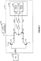
- FIG. 1 is a simplified schematic diagram of a current-mode buffer (alternatively referred to herein in as clock driver) 100 adapted to drive a high-frequency clock interconnect in accordance with one embodiment of the present invention.
- Clock driver 100 is shown as including PMOS transistors 104, 108, NMOS transistors 106, 110, inverters 112, 114, and control circuit 200.
- Control circuit 200 includes a biasing circuits 150 adapted to bias transistor 108, as well as biasing circuit 250 adapted to bias transistor 110.
- Clock driver 100 is shown as receiving an oscillating signal OSC from voltage-controlled oscillator (VCO) 102, and driving clock interconnect 200 that may be distributed throughout one or more sections of an Integrated Circuit in which it is disposed.
- Voltage-controlled oscillator 102 may be part of a phase locked-loop, frequency locked-loop or any other controlled-loop circuit.
- oscillating signal OSC is applied to the gate terminals of PMOS transistor 104 and NMOS transistors 106.
- the drain terminal of transistor 104 is coupled to the source terminal of transistors 108.
- the source terminal of transistor 110 is coupled to the drain terminal of transistor 106.
- the drain terminals of transistors 108, 110 are coupled to common node A and to the input terminal of inverter 112.
- the output terminal of inverter 112 is coupled to the input terminal of inverter 114 whose output terminal is coupled to the input terminals IN of biasing circuits 150, 250.
- the output terminal of biasing circuit 150 is coupled to the gate terminal of transistor 108.
- the output terminal of biasing circuit 250 is coupled to the gate terminal of transistor 110.
- Biasing circuit 150 is adapted to cause transistor 108 to be on when transistor 104 is on. Biasing circuit 150 is further adapted to cause transistor 108 to be off when transistor 104 is off. Likewise biasing circuit 250 is adapted to cause transistor 110 to be on when transistor 106 is on/off. Biasing circuit 250 is further adapted to cause transistor 108 to be off when transistor 104 is off.
- node A is charged to supply voltage Vcc via transistors 104, 108.
- transistor 106 is on and transistor 104 is off, because transistors 108, 110 are off and on respectively, node A is discharged to the ground potential via transistors 110, 106.
- the voltage at node A is buffered via inverters 112, 114 and applied to the input terminals IN of biasing circuits 150, 250.
- Node B coupled to the source terminal of transistor 108, supplies a signal to clock interconnect 200, which in turn, is adapted to provide clock signals to various blocks of an integrated circuit in which clock diver 100 is disposed.
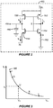
- FIG. 2 is a simplified transistor schematic diagram of an exemplary biasing circuit 150, in accordance with one embodiment of the present invention.
- Biasing circuit 150 is shown as including PMOS transistors 152, 156, NMOS transistors 154, 158, capacitor 160 and resistor 162.
- Transistors 152, 156 have the same gate-to-source voltage and form a current mirror.
- Resistor 162 is adapted to maintain the voltage of the source terminal of transistor 154, i.e., node D, above the ground potential. For example, in one embodiment, when the supply voltage VCC is 1.2 volts, node D is at 0.2 volts.
- Capacitor 160 has a first terminal coupled to the ground potential. The second terminal of capacitor 160 is coupled to node nbias and to the drain terminals of transistors 156, 158.
- Biasing circuit 150 is adapted to operate differentially to compare the voltages of source terminals of transistors 154 and 158 to detect the minimum voltage of the source terminal of transistor 158, i.e., the minimum voltage of terminal IN.
- PMOS transistors 152, 156 form a current mirror and thus generate the same current I 1 . Accordingly, if the voltage at de IN increases, because of the decrease in the gate-to-source voltage of transistor 158, the current through transistor 158 decreases. Since the current I 1 flowing through transistor 156 is relatively constant, the decrease in the current flow through transistor 158 causes more current to flow and charge capacitor 160, thereby causing the voltage of node nbias to increase.
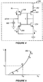
- Figure 3 shows a plot 180 indicating the relationship between the current flow I 2 through transistor 158 and the voltage V IN received by the source terminal of transistor 158.
- current I 2 has an inverse relationship with voltage V IN , decreasing when V IN increases and increasing when V IN decreases.
- Voltage V D of node D and the corresponding current I I flowing through node D is identified in plot 180 as point D'.
- plot 180 has a relatively high slope when voltage V IN is small (for example, between points F and G), and a relatively low slope when voltage V N is large (for example, between points K and L). Accordingly, the voltage across capacitor 160 is mostly defined by the near minimum values of voltage V IN .
- biasing circuit 150 is a minimum peak detector adapted to detect the near minimum value of voltage V IN -seen by its input terminal IN-and generate a voltage at its output terminal nbais that is defined by the detected minimum voltage. The larger the voltage swing at node IN and thereby the longer the time when the voltage at node IN is smaller than the voltage of node D, the greater is the voltage at node nbias.
- output terminal nbias of biasing circuit 150 is coupled to the gate terminal of transistor 110.
- FIG. 4 is a simplified transistor schematic diagram of an exemplary biasing circuit 250, in accordance with one embodiment of the present invention.
- Biasing circuit 250 is shown as including PMOS transistors 252, 256, NMOS transistors 254, 258, capacitor 260 and resistor 262.
- Transistors 258, 254 have the same gate-to-source voltage and form a current mirror.
- Resistor 262 is adapted to maintain the voltage at the source terminal of transistor 154, i.e., node M, below the supply voltage Vcc. For example, in one embodiment, when the supply voltage VCC is 1.2 volts, node M may be at 1.0 volts.
- Capacitor 260 has a first terminal coupled to the ground potential.
- the second terminal of capacitor 260 is coupled to node pbias and to the drain terminals of transistors 256, 258.
- Biasing circuit 250 is adapted to operate differentially to compare the voltages of source terminals of transistors 256 and 262 to detect the peak voltage of the source terminal of transistor 256, i.e., the peak voltage of terminal IN.
- NMOS transistors 254, 258 form a current mirror and thus generate the same current I 3 . Accordingly, if the voltage at node (terminal) IN increases, because of the increase in the gate-to-source voltage of transistor 256, the current through transistor 256 increases. Since the current I 3 flowing through transistor 258 is relatively constant, the increase in the current flow through transistor 256 causes more current to flow and charge capacitor 260, thereby causing the voltage of node pbias to increase.
- Figure 5 shows a plot 280 indicating the relationship between the current flow I 4 through transistor 258 and the voltage V IN received by the source terminal of transistor 258.
- current I 4 has a direct relationship with voltage V IN , decreasing when V IN decreases, and increasing when V IN increases.
- Voltage V M of node M and the corresponding current I 3 flowing through node M is identified in plot 180 as point M'.
- plot 280 has a relatively high slope when voltage V IN is large (for example, between points P and Q), and a relatively low slope when voltage V IN is small (for example, between points N and O). Accordingly, the voltage across capacitor 260 is mostly defined by the near maxim values of voltage V IN .
- biasing circuit 250 is a peak detector adapted to detect the near peak value of voltage V IN -seen by its input terminal IN-and generate a voltage at its output terminal pbais that is defined by this detected peak voltage. The larger the voltage swing at node IN and thereby the longer the time when the voltage at node IN is larger than the voltage of node M, the greater is the DC voltage at node pbias.
- output terminal pbias of biasing circuit 250 is coupled to the gate terminal of transistor 108.
- FIG. 6 is a simplified schematic diagram of a current-mode clock driver 300 adapted to drive a high-frequency clock interconnect in accordance with another embodiment of the present invention.
- Clock driver 300 is similar to clock driver 100 except that clock driver 300 includes first and second variable conductivity circuits 208, 210 in place of transistors 108, 110 of clock driver 100.
- the drain terminal of transistor 104 is coupled to a first input terminal of variable conductivity circuit 208.
- the drain terminal of transistor 106 is coupled to a first input terminal of variable conductivity circuit 210.
- Output terminals pbias and nbias of control circuit 200 are respectively applied to the second input terminals of first and second conductivity circuits 208, 210.
- the output terminals of first and second conductivity circuits 208, 210 are coupled to a common node A and to the input terminals IN of first and second biasing circuits 150, 250.
- Biasing circuit 150 is adapted to cause variable conductivity circuit 208 to be on when transistor 104 is on. Biasing circuit 150 is further adapted to cause variable conductivity circuit 208 to be off when transistor 104 is off. Likewise biasing circuit 250 is adapted to cause variable conductivity circuit 210 to be on when transistor 106 is on/off. Biasing circuit 250 is further adapted to cause variable conductivity circuit 210 to be off when transistor 104 is off.
- variable conductivity circuits 208, 210 As the voltage swing of node IN increases and thereby the peak and minimum voltages of node IN increase and decrease respectively, the voltage at node pbias increases and the voltage at node nbias decreases. This causes variable conductivity circuits 208, 210 to become less conductive, thereby causing the voltage swing of node IN to decrease. Likewise, as the voltage swing of node IN decreases, the voltage at node pbias decreases and the voltage at node nbias increases. This causes variable conductivity circuits 208, 210 to become more conductive, thereby causing the voltage swing of node IN to increase. Accordingly, the feedback loop formed by variable conductivity circuits 208, 210 and control circuitry 200 is adapted to minimize the variations of the voltage at node IN.
Landscapes
- Physics & Mathematics (AREA)
- Nonlinear Science (AREA)
- Amplifiers (AREA)
- Logic Circuits (AREA)
- Manipulation Of Pulses (AREA)
Description
- The present invention relates to Integrated Circuits (IC), and more particularly to a high-frequency clock interconnect circuit used in ICs.
- An IC often includes a clock interconnect circuit adapted to generate a multitude of clock signals that control the operations of the various blocks disposed in the IC. Controlling the variation in the arrival times of the clock signals, commonly referred to as clock skew, is important.
- Clock skew is dependent on two main parameters, namely the loading seen by the clock signal, as well as the RC delay of the clock interconnect. As is well known, clock skew increases the cycle times and reduces the rate at which the IC can operate. A number of different clock drivers have been developed to compensate for the differential delays of individual clock signals in order to minimize clock skew.
- As the operating frequency of an IC increases, the power consumption of various components of a clock distribution circuit, such as the local oscillator (LO) and the phase locked-loop (PLL), starts to increase. To reduce the power consumption at high frequencies, current-mode clock drivers/buffers have been developed. Conventional current-mode clock drivers, however, are designed to operate under worst case voltage, temperature and process conditions. As such, conventional current-mode buffers are not power efficient. Controlling the power consumption of a clock interconnect circuit operating at relatively high frequencies remains a challenge.
- Document
US 6 177 819 B1 refers to an IC driver circuit having an adjustable trip point. The driver circuit automatically adjusts the trip point of the circuit based on the state of the output signal (and thus, by inference, on the state of the input signal), by using first and second switches to couple and decouple secondary pullup and pulldown circuits. -
Document EP 1 014 584 A1 refers to a data transmitter comprising a driver for transmitting data, a receiver for receiving data transmitted from the driver, a transmission line for connecting the driver to the receiver, and a variable impedance element having a variably controllable impedance. The variable impedance element is connected to the transmission line. - Document
US 2008/201596 A1 refers to a clock buffer circuit of a semiconductor device which receives an external clock signal and generates an internal clock signal with no duty distortion. The clock buffer circuit includes a first clock buffer for receiving and buffering a normal-phase clock signal, a second clock buffer for receiving and buffering a reverse-phase clock signal, and an internal clock generator for generating an internal clock signal in response to output signals from the first and second clock buffers. - In accordance with the present invention, an apparatus as set forth in
claim 1, and a method as set forth in claim 10 are provided. Further embodiments of the invention are claimed in the dependent claims. - A current-mode driver circuit, in accordance with one embodiment of the present invention includes, in part, a first PMOS transistor, a first NMOS transistor, first and second variable conductivity circuits, and a control circuit. The first PMOS transistor has a gate terminal receiving an oscillating signal and a source terminal receiving a first supply voltage. The first NMOS transistor has a gate terminal receiving the oscillating signal and a source terminal receiving a second supply voltage. The first variable conductivity circuit has a first input terminal coupled to a drain terminal of the first PMOS transistor and an output terminal coupled to a common node. The second variable conductivity circuit has a first input terminal coupled to a drain terminal of the first NMOS transistor and an output terminal coupled to the common node. The control circuit is adapted to increase the conductivities of the first and second variable conductivity circuits in response to decreases in voltage swing of the common node, and further to decrease the conductivities of the first and second variable conductivity circuits in response to increases in voltage swing of the common node.
- The first variable conductivity circuit is a PMOS transistor (second PMOS transistor) having a source terminal coupled to the drain terminal of the first PMOS transistor and a drain terminal coupled to the common node. The second variable conductivity circuit is an NMOS transistor (second NMOS transistor) having a source terminal coupled to the drain terminal of the first NMOS transistor and a drain terminal coupled to the common node.
- The current-mode clock driver circuit further includes a first biasing circuit that, in turn, includes a first current mirror, a first capacitor, and a first differential amplifier. The first differential amplifier includes a third NMOS transistor whose source terminal is responsive to the voltage of the common node. The first differential amplifier further includes a fourth NMOS transistor receiving the current generated by the first current mirror and having a gate terminal coupled to the gate terminal of the third NMOS transistor.
- In one embodiment, the first biasing circuit further includes, in part, a resistive element coupled between the source terminal of the fourth NMOS transistor and the second supply voltage. In one embodiment, the voltage across the first capacitor is defined by a difference between the current supplied by the first current mirror and the current flowing through the third NMOS transistor.
- In one embodiment, the current-mode clock driver circuit further includes a second biasing circuit that, in turn, includes a second current mirror, a second capacitor, and a second differential amplifier. The second differential amplifier includes a third PMOS transistor whose source terminal is responsive to the voltage of the common node. The second differential amplifier further includes a fourth PMOS transistor receiving a current generated by the second current mirror and having a gate terminal coupled to the gate terminal of the third PMOS transistor.
- In one embodiment, the voltage across the second capacitor is defined by the difference between the current supplied by the second current mirror and the current flowing through the third PMOS transistor. In one embodiment, the voltage across the first capacitor is applied to the gate terminal of the second NMOS transistor, and the voltage across the second capacitor is applied to the gate terminal of the second PMOS transistor.
- A method of driving a clock interconnect, according to the invention, includes applying an oscillating signal to the gate terminal of a first PMOS transistor whose source terminal receives a first supply voltage, applying the oscillating signal to the gate terminal of a first NMOS transistor whose source terminal receives a second supply voltage, coupling the drain terminal of the first PMOS transistor to a first input terminal of a first variable conductivity circuit, coupling the drain terminal of the first NMOS transistor to a first input terminal of a second variable conductivity circuit, coupling output terminals of the first and second variable conductivity circuits to a common node, increasing conductivities of the first and second variable conductivity circuits in response to decreases in voltage swing of the common node, and decreasing the conductivities of the first and second variable conductivity circuits in response to increases in voltage swing of the common node.
- The first variable conductivity circuit is a PMOS transistor (second PMOS transistor) having a source terminal coupled to the drain terminal of the first PMOS transistor, and a drain terminal coupled to the common node. The second variable conductivity circuit is an NMOS transistor (second NMOS transistor) having a source terminal coupled to the drain terminal of the first NMOS transistor and a drain terminal coupled to the common node.
- Varying the conductivity of the second NMOS transistor includes forming a first current mirror, coupling the first current mirror to a first capacitor, and forming a first differential amplifier. The first differential amplifier includes a third NMOS transistor whose source terminal is responsive to the voltage of the common node. The first differential amplifier may further include a fourth NMOS transistor that receives the current generated by the first current mirror and whose gate terminal is coupled to the gate terminal of the third NMOS transistor.
- The method, in accordance with one embodiment, further includes coupling a resistive element between the source terminal of the fourth NMOS transistor and the second supply voltage. The method, in accordance with one embodiment, further includes forming a voltage across the first capacitor defined by the difference between the current supplied by the first current mirror and the current flowing through the third NMOS transistor.
- In one embodiment, varying the conductivity of the second PMOS transistor includes forming a second current mirror, coupling the second current mirror to a second capacitor, and forming a second differential amplifier. The second differential amplifier may further include a third PMOS transistor whose source terminal is responsive to the voltage of the common node. The second differential amplifier may further include a fourth PMOS transistor that receives the current generated by the second current mirror and whose gate terminal is coupled to the gate terminal of the third PMOS transistor.
- The method, in accordance with one embodiment, further includes forming a voltage across the second capacitor defined by the difference between the current supplied by the second current mirror and the current flowing through the third PMOS transistor. The method further includes applying the voltage of the first capacitor to the gate terminal of the second NMOS transistor, and applying the voltage of the second capacitor to the gate terminal of the second PMOS transistor.
- A current-mode clock driver, in accordance with one embodiment of the present invention includes, in part, means for applying an oscillating signal to a gate terminal of a first PMOS transistor having a source terminal receiving a first supply voltage, means for applying the oscillating signal to a gate terminal of a first NMOS transistor a source terminal receiving a second supply voltage, means for coupling a drain terminal of the first PMOS transistor to a first input terminal of a first variable conductivity circuit, means for coupling a drain terminal of the first NMOS transistor to a first input terminal of a second variable conductivity circuit, means for coupling output terminals of the first and second variable conductivity circuits to a common node, means for increasing conductivities of the first and second variable conductivity circuits in response to decreases in voltage swing of the common node, and means for decreasing the conductivities of the first and second variable conductivity circuits in response to increases in voltage swing of the common node.
- In one embodiment, the first variable conductivity circuit is a PMOS transistor (second PMOS transistor) having a source terminal coupled to the drain terminal of the first PMOS transistor and a drain terminal coupled to the common node. The second variable conductivity circuit is an NMOS transistor (second NMOS transistor) having a source terminal coupled to the drain terminal of the first NMOS transistor and a drain terminal coupled to the common node.
- In one embodiment, the means for increasing or decreasing the conductivity of the second NMOS transistor further includes means for forming a first current mirror, means for coupling the first current mirror to a first capacitor, and means for forming a first differential amplifier having a third NMOS transistor whose source terminal is responsive to the voltage of the common node. The first differential amplifier may further include a fourth NMOS transistor that receives the current generated by the first current mirror and whose gate terminal is coupled to the gate terminal of the third NMOS transistor.
- In one embodiment, the current-mode clock driver further includes, in part, means for coupling a resistive element between a source terminal of the fourth NMOS transistor and the second supply voltage. In one embodiment, the current-mode clock driver further includes, in part, means for forming a first voltage across the first capacitor defined by the difference between the current supplied by the first current mirror and the current flowing through the third NMOS transistor.
- In one embodiment, the means for increasing or decreasing the conductivity of the second PMOS transistor further includes means for forming a second current mirror, means for coupling the second current mirror to a second capacitor, and means for forming a second differential amplifier having a third PMOS transistor whose source terminal is responsive to the voltage of the common node. The second differential amplifier may further include a fourth PMOS transistor that receives the current generated by the second current mirror and whose gate terminal is coupled to the gate terminal of the third PMOS transistor.
- In one embodiment, the current-mode clock driver further includes, in part, means for forming a second voltage across the second capacitor defined by the difference between the current supplied by the second current mirror and the current flowing through the third PMOS transistor.
- In one embodiment, the current-mode clock driver further includes, in part, means for applying the first voltage to the gate terminal of the second NMOS transistor, and means for applying the second voltage to the gate terminal of the second PMOS transistor.
- A non-transitory computer readable storage medium, in accordance with one embodiment of the present invention, includes instructions that when executed by a processor cause the processor to apply an oscillating signal to a gate terminal of a first PMOS transistor having a source terminal receiving a first supply voltage, apply the oscillating signal to a gate terminal of a first NMOS transistor having a source terminal receiving a second supply voltage, couple the drain terminal of the first PMOS transistor to a first input terminal of a first variable conductivity circuit, couple the drain terminal of the first NMOS transistor to a first input terminal of a second variable conductivity circuit, couple output terminals of the first and second variable conductivity circuits to a common node, increase conductivities of the first and second variable conductivity circuits in response to decreases in voltage swing of the common node, and decrease the conductivities of the first and second variable conductivity circuits in response to increases in voltage swing of the common node.
- In accordance with one embodiment, the first variable conductivity circuit is a PMOS transistor (second PMOS transistor) having a source terminal coupled to the drain terminal of the first PMOS transistor and a drain terminal coupled to the common node. The second variable conductivity circuit is an NMOS transistor (second NMOS transistor) having a source terminal coupled to the drain terminal of the first NMOS transistor, and a drain terminal coupled to the common node.
- In one embodiment, to vary the conductivity of the second NMOS transistor, the instructions further cause the processor to form a first current mirror, couple the first current mirror to a first capacitor, and form a first differential amplifier having a third NMOS transistor whose source terminal is responsive to the voltage of the common node. The first differential amplifier may further include a fourth NMOS transistor that receives the current generated by the first current mirror and whose gate terminal is coupled to the gate terminal of the third NMOS transistor.
- In one embodiment, the instructions further cause the processor to couple a resistive element between the source terminal of the fourth NMOS transistor and the second supply voltage. In one embodiment, the instructions further cause the processor to form a voltage across the first capacitor defined by the difference between the current supplied by the first current mirror and the current flowing through the third NMOS transistor.
- In one embodiment, to vary the conductivity of the second PMOS transistor, the instructions further cause the processor to form a second current mirror, couple the second current mirror to a second capacitor, and form a second differential amplifier having a third PMOS transistor whose source terminal is responsive to the voltage of the common node. The second differential amplifier may further include a fourth PMOS transistor that receives the current generated by the second current mirror and whose gate terminal is coupled to the gate terminal of the third PMOS transistor.
- In one embodiment, the instructions further cause the processor to form a voltage across the second capacitor defined by the difference between the current supplied by the second current mirror and the current flowing through the third PMOS transistor. In one embodiment, the instructions further cause the processor to apply the voltage of the first capacitor to the gate terminal of the second NMOS transistor, and apply the voltage of the second capacitor to the gate terminal of the second PMOS transistor.
-
-
Figure 1 is a simplified schematic diagram of a current-mode buffer adapted to drive a high-frequency clock interconnect, in accordance with one embodiment of the present invention. -
Figure 2 is a simplified transistor schematic diagram of one of the biasing circuits of the current-mode buffer ofFigure 1 , in accordance with one embodiment of the present invention. -
Figure 3 shows the relationship between the current flowing through and the source voltage of one of the transistors disposed in the biasing circuit ofFigure 2 . -
Figure 4 is a simplified transistor schematic diagram of another one of the biasing circuits of the current-mode buffer ofFigure 1 , in accordance with one embodiment of the present invention. -
Figure 5 shows the relationship between the current flowing through and the source voltage of one of the transistors disposed in the biasing circuit ofFigure 5 . -
Figure 6 is a simplified schematic diagram of a current-mode clock driver adapted to drive a high-frequency clock interconnect in accordance with another embodiment of the present invention. -
Figure 1 is a simplified schematic diagram of a current-mode buffer (alternatively referred to herein in as clock driver) 100 adapted to drive a high-frequency clock interconnect in accordance with one embodiment of the present invention.Clock driver 100 is shown as includingPMOS transistors NMOS transistors inverters control circuit 200.Control circuit 200 includes a biasingcircuits 150 adapted tobias transistor 108, as well as biasingcircuit 250 adapted tobias transistor 110. -
Clock driver 100 is shown as receiving an oscillating signal OSC from voltage-controlled oscillator (VCO) 102, and drivingclock interconnect 200 that may be distributed throughout one or more sections of an Integrated Circuit in which it is disposed. Voltage-controlledoscillator 102 may be part of a phase locked-loop, frequency locked-loop or any other controlled-loop circuit. As is seen fromFigure 1 , oscillating signal OSC is applied to the gate terminals ofPMOS transistor 104 andNMOS transistors 106. - When signal OSC is at a low value,
PMOS transistor 104 is on andNMOS transistor 106 is off. Accordingly, when signal OSC is at a low value, node B is enabled to charge to the supply voltage VCC viatransistor 104. Conversely, when signal OSC is at a high value,PMOS transistor 104 is off andNMOS transistor 106 is on. Accordingly, when signal OSC is at a high value, node C is enabled to discharge to the ground potential viatransistor 106. - The drain terminal of
transistor 104 is coupled to the source terminal oftransistors 108. Likewise, the source terminal oftransistor 110 is coupled to the drain terminal oftransistor 106. The drain terminals oftransistors inverter 112. The output terminal ofinverter 112 is coupled to the input terminal ofinverter 114 whose output terminal is coupled to the input terminals IN of biasingcircuits circuit 150 is coupled to the gate terminal oftransistor 108. Likewise, the output terminal of biasingcircuit 250 is coupled to the gate terminal oftransistor 110. -
Biasing circuit 150 is adapted to causetransistor 108 to be on whentransistor 104 is on.Biasing circuit 150 is further adapted to causetransistor 108 to be off whentransistor 104 is off. Likewise biasingcircuit 250 is adapted to causetransistor 110 to be on whentransistor 106 is on/off.Biasing circuit 250 is further adapted to causetransistor 108 to be off whentransistor 104 is off. - Accordingly, when
transistor 104 is on andtransistor 106 is off, becausetransistors transistors transistor 106 is on andtransistor 104 is off, becausetransistors transistors inverters circuits transistor 108, supplies a signal toclock interconnect 200, which in turn, is adapted to provide clock signals to various blocks of an integrated circuit in whichclock diver 100 is disposed. -
Figure 2 is a simplified transistor schematic diagram of anexemplary biasing circuit 150, in accordance with one embodiment of the present invention.Biasing circuit 150 is shown as includingPMOS transistors NMOS transistors capacitor 160 andresistor 162.Transistors Resistor 162 is adapted to maintain the voltage of the source terminal oftransistor 154, i.e., node D, above the ground potential. For example, in one embodiment, when the supply voltage VCC is 1.2 volts, node D is at 0.2 volts. - The gate terminals of
transistors 152, 154,156 and 158 are coupled to one another. The gate and drain terminals oftransistors Capacitor 160 has a first terminal coupled to the ground potential. The second terminal ofcapacitor 160 is coupled to node nbias and to the drain terminals oftransistors -
Biasing circuit 150 is adapted to operate differentially to compare the voltages of source terminals oftransistors transistor 158, i.e., the minimum voltage of terminal IN. As described above,PMOS transistors transistor 158, the current throughtransistor 158 decreases. Since the current I1 flowing throughtransistor 156 is relatively constant, the decrease in the current flow throughtransistor 158 causes more current to flow andcharge capacitor 160, thereby causing the voltage of node nbias to increase. - Conversely, if the voltage at node IN decreases, because of the increase in the gate-to-source voltage of
transistor 158, the current throughtransistor 158 increases. Since the current I1 flowing throughtransistor 156 is relatively constant, the increase in the current flow throughtransistor 158 causes current to be withdrawn fromcapacitor 160, thereby causing the voltage of node nbias to decrease. -
Figure 3 shows aplot 180 indicating the relationship between the current flow I2 throughtransistor 158 and the voltage VIN received by the source terminal oftransistor 158. As seen fromFigure 3 , current I2 has an inverse relationship with voltage VIN, decreasing when VIN increases and increasing when VIN decreases. Voltage VD of node D and the corresponding current II flowing through node D is identified inplot 180 as point D'. - As is seen from
Figure 3 ,plot 180 has a relatively high slope when voltage VIN is small (for example, between points F and G), and a relatively low slope when voltage VN is large (for example, between points K and L). Accordingly, the voltage acrosscapacitor 160 is mostly defined by the near minimum values of voltage VIN. In other words, biasingcircuit 150 is a minimum peak detector adapted to detect the near minimum value of voltage VIN-seen by its input terminal IN-and generate a voltage at its output terminal nbais that is defined by the detected minimum voltage. The larger the voltage swing at node IN and thereby the longer the time when the voltage at node IN is smaller than the voltage of node D, the greater is the voltage at node nbias. As is seen fromFigure 1 , output terminal nbias of biasingcircuit 150 is coupled to the gate terminal oftransistor 110. -
Figure 4 is a simplified transistor schematic diagram of anexemplary biasing circuit 250, in accordance with one embodiment of the present invention.Biasing circuit 250 is shown as includingPMOS transistors NMOS transistors capacitor 260 andresistor 262.Transistors Resistor 262 is adapted to maintain the voltage at the source terminal oftransistor 154, i.e., node M, below the supply voltage Vcc. For example, in one embodiment, when the supply voltage VCC is 1.2 volts, node M may be at 1.0 volts. - The gate terminals of
transistors transistors Capacitor 260 has a first terminal coupled to the ground potential. The second terminal ofcapacitor 260 is coupled to node pbias and to the drain terminals oftransistors -
Biasing circuit 250 is adapted to operate differentially to compare the voltages of source terminals oftransistors transistor 256, i.e., the peak voltage of terminal IN. As described above,NMOS transistors transistor 256, the current throughtransistor 256 increases. Since the current I3 flowing throughtransistor 258 is relatively constant, the increase in the current flow throughtransistor 256 causes more current to flow andcharge capacitor 260, thereby causing the voltage of node pbias to increase. - Conversely, if the voltage at node IN decreases, because of the decrease in the gate-to-source voltage of
transistor 256, the current throughtransistor 256 decreases. Since the current I3 flowing throughtransistor 258 is relatively constant, the decrease in the current flow throughtransistor 256 causes capacitor 260 to discharge, thereby causing the voltage of node pbias to decrease. -
Figure 5 shows aplot 280 indicating the relationship between the current flow I4 throughtransistor 258 and the voltage VIN received by the source terminal oftransistor 258. As seen fromFigure 5 , current I4 has a direct relationship with voltage VIN, decreasing when VIN decreases, and increasing when VIN increases. Voltage VM of node M and the corresponding current I3 flowing through node M is identified inplot 180 as point M'. - As is seen from
Figure 5 ,plot 280 has a relatively high slope when voltage VIN is large (for example, between points P and Q), and a relatively low slope when voltage VIN is small (for example, between points N and O). Accordingly, the voltage acrosscapacitor 260 is mostly defined by the near maxim values of voltage VIN. In other words, biasingcircuit 250 is a peak detector adapted to detect the near peak value of voltage VIN-seen by its input terminal IN-and generate a voltage at its output terminal pbais that is defined by this detected peak voltage. The larger the voltage swing at node IN and thereby the longer the time when the voltage at node IN is larger than the voltage of node M, the greater is the DC voltage at node pbias. As is seen fromFigure 1 , output terminal pbias of biasingcircuit 250 is coupled to the gate terminal oftransistor 108. - Referring to
Figures 1 ,2 and4 concurrently, as the voltage swing of node IN increases and thereby the peak and minimum voltages of node IN increase and decrease respectively, the voltage at node pbias increases and the voltage at node nbias decreases. This causestransistors transistors transistors control circuitry 200 is adapted to minimize the variations of the voltage at node IN. -
Figure 6 is a simplified schematic diagram of a current-mode clock driver 300 adapted to drive a high-frequency clock interconnect in accordance with another embodiment of the present invention.Clock driver 300 is similar toclock driver 100 except thatclock driver 300 includes first and secondvariable conductivity circuits transistors clock driver 100. - The drain terminal of
transistor 104 is coupled to a first input terminal ofvariable conductivity circuit 208. Likewise, the drain terminal oftransistor 106 is coupled to a first input terminal ofvariable conductivity circuit 210. Output terminals pbias and nbias ofcontrol circuit 200 are respectively applied to the second input terminals of first andsecond conductivity circuits second conductivity circuits second biasing circuits -
Biasing circuit 150 is adapted to causevariable conductivity circuit 208 to be on whentransistor 104 is on.Biasing circuit 150 is further adapted to causevariable conductivity circuit 208 to be off whentransistor 104 is off. Likewise biasingcircuit 250 is adapted to causevariable conductivity circuit 210 to be on whentransistor 106 is on/off.Biasing circuit 250 is further adapted to causevariable conductivity circuit 210 to be off whentransistor 104 is off. - As the voltage swing of node IN increases and thereby the peak and minimum voltages of node IN increase and decrease respectively, the voltage at node pbias increases and the voltage at node nbias decreases. This causes
variable conductivity circuits variable conductivity circuits variable conductivity circuits control circuitry 200 is adapted to minimize the variations of the voltage at node IN. - The above embodiments of the present invention are illustrative and not limitative.
Claims (15)
- A current-mode driver circuit (100) comprising:a first PMOS transistor (104) having a gate terminal receiving an oscillating signal and a source terminal receiving a first supply voltage;a first NMOS transistor (106) having a gate terminal receiving the oscillating signal and a source terminal receiving a second supply voltage;a second PMOS transistor (108) having a source terminal coupled to a drain terminal of the first PMOS transistor (104) and a drain terminal coupled to a common node (A);a second NMOS transistor (110) having a source terminal coupled to a drain terminal of the first NMOS transistor (106), and a drain terminal coupled to the common node (A); anda control circuit (200) adapted to increase conductivities of the second PMOS transistor and the second NMOS transistor (108, 110) in response to decreases in voltage swing of the common node (A), said control circuit (200) further adapted to decrease the conductivities of the second PMOS transistor and the second NMOS transistor (108, 110) in response to increases in voltage swing of the common node (A); and wherein the control circuit (200) comprises a first biasing circuit (150), said first biasing circuit (150) comprising:a first current mirror;a first capacitor (160); anda first differential amplifier comprising a third NMOS transistor having a source terminal responsive to the voltage of the common node (A).
- The current-mode clock driver circuit (100) of claim 1 wherein the first differential amplifier further comprises a fourth NMOS transistor receiving a current generated by the first current mirror and having a gate terminal coupled to a gate terminal of the third NMOS transistor.
- The current-mode clock driver circuit (100) of claim 2, further comprising a resistive element coupled between a source terminal of the fourth NMOS transistor and the second supply voltage.
- The current-mode clock driver circuit (100) of claim 3 wherein a voltage across the first capacitor (160) is defined by a difference between a current supplied by the first current mirror and a current flowing through the third NMOS transistor.
- The current-mode clock driver circuit (100) of claim 4, wherein the control circuit (200) further comprises a second biasing circuit, said second biasing circuit comprising:a second current mirror;a second capacitor; anda second differential amplifier comprising a third PMOS transistor having a source terminal responsive to the voltage of the common node.
- The current-mode clock driver circuit (100) of claim 5 wherein the second differential amplifier further comprises a fourth PMOS transistor receiving a current generated by the second current mirror and having a gate terminal coupled to a gate terminal of the third PMOS transistor.
- The current-mode clock driver circuit (100) of claim 6, wherein a voltage across the second capacitor is defined by a difference between a current supplied by the second current mirror and a current flowing through the third PMOS transistor.
- The current-mode clock driver (100) of claim 7 wherein the voltage across the first capacitor (160) is applied to a gate terminal of the second NMOS transistor.
- The current-mode clock driver circuit (100) of claim 8, wherein the voltage across the second capacitor is applied to a gate terminal of the second PMOS transistor.
- A method of driving a clock interconnect, the method comprising:applying an oscillating signal to a gate terminal of a first PMOS transistor (104) having a source terminal receiving a first supply voltage;applying the oscillating signal to a gate terminal of a first NMOS transistor (106) having a source terminal receiving a second supply voltage;coupling a drain terminal of the first PMOS transistor (104) to a source terminal of a second PMOS transistor (108);coupling a drain terminal of the first NMOS transistor (106) to a source terminal of a second NMOS transistor (110);coupling drain terminals of the second PMOS transistor and the second NMOS transistor (108, 110) to a common node (A);increasing conductivities of the second PMOS transistor and the second NMOS transistor (108, 110) in response to decreases in voltage swing of the common node (A); anddecreasing the conductivities of the second PMOS transistor and the second NMOS transistor (108, 110) in response to increases in voltage swing of the common node (A); and wherein increasing or decreasing the conductivity of the second PMOS transistor and the second NMOS transistor (108, 110) comprises:forming a first current mirror;coupling the first current mirror to a first capacitor (160); andforming a first differential amplifier comprising a third NMOS transistor having a source terminal responsive to the voltage of the common node (A).
- The method of claim 10 wherein the first differential amplifier further comprises a fourth NMOS transistor receiving a current generated by the first current mirror and having a gate terminal coupled to a gate terminal of the third NMOS transistor, and further comprising:
coupling a resistive element between a source terminal of the fourth NMOS transistor and the second supply voltage. - The method of claim 11 further comprising:
forming a voltage across the first capacitor (160) defined by a difference between a current supplied by the first current mirror and a current flowing through the third NMOS transistor, and wherein varying the conductivity of the second PMOS transistor comprises:forming a second current mirror;coupling the second current mirror to a second capacitor; andforming a second differential amplifier comprising a third PMOS transistor having a source terminal responsive to the voltage of the common node. - The method of claim 12 wherein the second differential amplifier further comprises a fourth PMOS transistor receiving a current generated by the second current mirror and having a gate terminal coupled to a gate terminal of the third PMOS transistor, and further comprising:
forming a voltage across the second capacitor defined by a difference between a current supplied by the second current mirror and a current flowing through the third PMOS transistor. - The method of claim 13 further comprising:
applying the voltage of the first capacitor (160) to a gate terminal of the second NMOS transistor and further comprising:
applying the voltage of the second capacitor to a gate terminal of the second PMOS transistor. - A non-transitory computer readable storage medium comprising instructions that when executed by a processor cause the processor to carry out the method steps of any of claims 10 to 14.
Applications Claiming Priority (2)
| Application Number | Priority Date | Filing Date | Title |
|---|---|---|---|
| US13/834,861 US8766674B1 (en) | 2013-03-15 | 2013-03-15 | Current-mode buffer with output swing detector for high frequency clock interconnect |
| PCT/US2014/023684 WO2014150581A1 (en) | 2013-03-15 | 2014-03-11 | Current-mode buffer with output swing detector for high frequency clock interconnect |
Publications (2)
| Publication Number | Publication Date |
|---|---|
| EP2974020A1 EP2974020A1 (en) | 2016-01-20 |
| EP2974020B1 true EP2974020B1 (en) | 2019-02-27 |
Family
ID=50434295
Family Applications (1)
| Application Number | Title | Priority Date | Filing Date |
|---|---|---|---|
| EP14715182.3A Not-in-force EP2974020B1 (en) | 2013-03-15 | 2014-03-11 | Current-mode buffer with output swing detector for high frequency clock interconnect |
Country Status (6)
| Country | Link |
|---|---|
| US (1) | US8766674B1 (en) |
| EP (1) | EP2974020B1 (en) |
| JP (1) | JP6419770B2 (en) |
| KR (1) | KR20150131141A (en) |
| CN (1) | CN105191128B (en) |
| WO (1) | WO2014150581A1 (en) |
Families Citing this family (3)
| Publication number | Priority date | Publication date | Assignee | Title |
|---|---|---|---|---|
| US9985644B1 (en) * | 2018-01-16 | 2018-05-29 | Realtek Semiconductor Corp. | Digital to-time converter and method therof |
| US10219339B1 (en) * | 2018-02-19 | 2019-02-26 | Ixys, Llc | Current correction techniques for accurate high current short channel driver |
| FR3102581B1 (en) * | 2019-10-23 | 2021-10-22 | St Microelectronics Rousset | Voltage Regulator |
Family Cites Families (22)
| Publication number | Priority date | Publication date | Assignee | Title |
|---|---|---|---|---|
| US4539489A (en) * | 1983-06-22 | 1985-09-03 | Motorola, Inc. | CMOS Schmitt trigger circuit |
| US5459437A (en) * | 1994-05-10 | 1995-10-17 | Integrated Device Technology | Logic gate with controllable hysteresis and high frequency voltage controlled oscillator |
| US5497127A (en) * | 1994-12-14 | 1996-03-05 | David Sarnoff Research Center, Inc. | Wide frequency range CMOS relaxation oscillator with variable hysteresis |
| US5726596A (en) * | 1996-03-01 | 1998-03-10 | Hewlett-Packard Company | High-performance, low-skew clocking scheme for single-phase, high-frequency global VLSI processor |
| US6323756B1 (en) * | 1997-09-02 | 2001-11-27 | Matsushita Electric Industrial Co., Ltd. | Data transmitter |
| US5939937A (en) * | 1997-09-29 | 1999-08-17 | Siemens Aktiengesellschaft | Constant current CMOS output driver circuit with dual gate transistor devices |
| JP3152204B2 (en) * | 1998-06-02 | 2001-04-03 | 日本電気株式会社 | Slew rate output circuit |
| US6177819B1 (en) * | 1999-04-01 | 2001-01-23 | Xilinx, Inc. | Integrated circuit driver with adjustable trip point |
| JP3520913B2 (en) * | 2000-06-09 | 2004-04-19 | 日本電気株式会社 | Signal line control method |
| US6316977B1 (en) * | 2000-07-14 | 2001-11-13 | Pmc-Sierra, Inc. | Low charge-injection charge pump |
| US6356106B1 (en) * | 2000-09-12 | 2002-03-12 | Micron Technology, Inc. | Active termination in a multidrop memory system |
| US7493149B1 (en) | 2002-03-26 | 2009-02-17 | National Semiconductor Corporation | Method and system for minimizing power consumption in mobile devices using cooperative adaptive voltage and threshold scaling |
| JP4869569B2 (en) | 2004-06-23 | 2012-02-08 | 株式会社 日立ディスプレイズ | Display device |
| KR100890041B1 (en) * | 2006-12-29 | 2009-03-25 | 주식회사 하이닉스반도체 | Clock buffer circuit of semiconductor device |
| US7502719B2 (en) | 2007-01-25 | 2009-03-10 | Monolithic Power Systems, Inc. | Method and apparatus for overshoot and undershoot errors correction in analog low dropout regulators |
| US7652511B2 (en) * | 2008-01-16 | 2010-01-26 | Amazing Microelectronic Corp. | Slew-rate control circuitry with output buffer and feedback |
| CN101540603A (en) | 2008-03-21 | 2009-09-23 | 意法半导体研发(上海)有限公司 | Efficacy push-pull buffer circuit, system and method for high frequency signals |
| US7902904B2 (en) * | 2008-12-09 | 2011-03-08 | Lsi Corporation | Bias circuit scheme for improved reliability in high voltage supply with low voltage device |
| US8149023B2 (en) * | 2009-10-21 | 2012-04-03 | Qualcomm Incorporated | RF buffer circuit with dynamic biasing |
| KR20110132864A (en) | 2010-06-03 | 2011-12-09 | 삼성전자주식회사 | Phase interpolation circuit for use in wide range frequency inputs and output securing method thereof |
| JP5545751B2 (en) * | 2010-11-25 | 2014-07-09 | 三菱電機株式会社 | Peak hold circuit and bottom hold circuit |
| US8860469B1 (en) * | 2012-07-13 | 2014-10-14 | Altera Corporation | Apparatus and methods for transmitter output swing calibration |
-
2013
- 2013-03-15 US US13/834,861 patent/US8766674B1/en active Active
-
2014
- 2014-03-11 EP EP14715182.3A patent/EP2974020B1/en not_active Not-in-force
- 2014-03-11 KR KR1020157028287A patent/KR20150131141A/en not_active Application Discontinuation
- 2014-03-11 WO PCT/US2014/023684 patent/WO2014150581A1/en active Application Filing
- 2014-03-11 CN CN201480014291.8A patent/CN105191128B/en active Active
- 2014-03-11 JP JP2016501316A patent/JP6419770B2/en not_active Expired - Fee Related
Non-Patent Citations (1)
| Title |
|---|
| None * |
Also Published As
| Publication number | Publication date |
|---|---|
| US8766674B1 (en) | 2014-07-01 |
| CN105191128A (en) | 2015-12-23 |
| JP6419770B2 (en) | 2018-11-07 |
| WO2014150581A1 (en) | 2014-09-25 |
| CN105191128B (en) | 2018-06-12 |
| KR20150131141A (en) | 2015-11-24 |
| JP2016518732A (en) | 2016-06-23 |
| EP2974020A1 (en) | 2016-01-20 |
Similar Documents
| Publication | Publication Date | Title |
|---|---|---|
| US20140312928A1 (en) | High-Speed Current Steering Logic Output Buffer | |
| US6670821B2 (en) | Methods and systems for sensing and compensating for process, voltage, temperature, and load variations | |
| KR100968459B1 (en) | Semiconductor Memory Apparatus | |
| US7463101B2 (en) | Voltage controlled oscillator with temperature and process compensation | |
| US8212596B2 (en) | PLL circuit | |
| US8508304B2 (en) | Serdes VCO with phased outputs driving frequency to voltage converter | |
| EP2974020B1 (en) | Current-mode buffer with output swing detector for high frequency clock interconnect | |
| US8536917B2 (en) | Duty cycle adjustment circuit | |
| CN112042122B (en) | Power supply compensation delay unit | |
| US20080068097A1 (en) | Voltage controlled oscillator and method capable of reducing phase noise and jitter with startup gain | |
| US8022740B2 (en) | Fast-response phase-locked loop charge-pump driven by low voltage input | |
| US9742413B2 (en) | Electronic device and information processing apparatus | |
| EP2916441B1 (en) | Charge pump circuit | |
| US20170170836A1 (en) | Voltage Controlled Oscillator and Phase Locked Loop Comprising the Same | |
| US8081040B1 (en) | Method and apparatus for oscillating | |
| US10587252B2 (en) | Skew compensation circuit | |
| US8933741B1 (en) | Method and apparatus for generating delay | |
| WO2017149957A1 (en) | Signal output circuit | |
| US7242255B1 (en) | Method and apparatus for minimizing phase error and jitter in a phase-locked loop | |
| TWI445334B (en) | Signal transmission system and signal transmission method thereof | |
| US20160191030A1 (en) | Voltage controlled delay circuit and voltage controlled oscillator including the same | |
| JP7351632B2 (en) | Integrated circuits containing phase-locked loop circuits | |
| TW201304424A (en) | Oscillating signal generating apparatus and control signal generator of the oscillating signal generating apparatus | |
| TW201828605A (en) | Band selected clock data recovery circuit and associated method | |
| JP6559548B2 (en) | Oscillator circuit device |
Legal Events
| Date | Code | Title | Description |
|---|---|---|---|
| PUAI | Public reference made under article 153(3) epc to a published international application that has entered the european phase |
Free format text: ORIGINAL CODE: 0009012 |
|
| 17P | Request for examination filed |
Effective date: 20150820 |
|
| AK | Designated contracting states |
Kind code of ref document: A1 Designated state(s): AL AT BE BG CH CY CZ DE DK EE ES FI FR GB GR HR HU IE IS IT LI LT LU LV MC MK MT NL NO PL PT RO RS SE SI SK SM TR |
|
| AX | Request for extension of the european patent |
Extension state: BA ME |
|
| DAX | Request for extension of the european patent (deleted) | ||
| STAA | Information on the status of an ep patent application or granted ep patent |
Free format text: STATUS: EXAMINATION IS IN PROGRESS |
|
| 17Q | First examination report despatched |
Effective date: 20170411 |
|
| GRAP | Despatch of communication of intention to grant a patent |
Free format text: ORIGINAL CODE: EPIDOSNIGR1 |
|
| STAA | Information on the status of an ep patent application or granted ep patent |
Free format text: STATUS: GRANT OF PATENT IS INTENDED |
|
| INTG | Intention to grant announced |
Effective date: 20180711 |
|
| GRAJ | Information related to disapproval of communication of intention to grant by the applicant or resumption of examination proceedings by the epo deleted |
Free format text: ORIGINAL CODE: EPIDOSDIGR1 |
|
| GRAL | Information related to payment of fee for publishing/printing deleted |
Free format text: ORIGINAL CODE: EPIDOSDIGR3 |
|
| GRAS | Grant fee paid |
Free format text: ORIGINAL CODE: EPIDOSNIGR3 |
|
| STAA | Information on the status of an ep patent application or granted ep patent |
Free format text: STATUS: EXAMINATION IS IN PROGRESS |
|
| GRAR | Information related to intention to grant a patent recorded |
Free format text: ORIGINAL CODE: EPIDOSNIGR71 |
|
| STAA | Information on the status of an ep patent application or granted ep patent |
Free format text: STATUS: GRANT OF PATENT IS INTENDED |
|
| GRAJ | Information related to disapproval of communication of intention to grant by the applicant or resumption of examination proceedings by the epo deleted |
Free format text: ORIGINAL CODE: EPIDOSDIGR1 |
|
| GRAR | Information related to intention to grant a patent recorded |
Free format text: ORIGINAL CODE: EPIDOSNIGR71 |
|
| INTC | Intention to grant announced (deleted) | ||
| INTG | Intention to grant announced |
Effective date: 20181206 |
|
| INTG | Intention to grant announced |
Effective date: 20181217 |
|
| GRAA | (expected) grant |
Free format text: ORIGINAL CODE: 0009210 |
|
| STAA | Information on the status of an ep patent application or granted ep patent |
Free format text: STATUS: THE PATENT HAS BEEN GRANTED |
|
| AK | Designated contracting states |
Kind code of ref document: B1 Designated state(s): AL AT BE BG CH CY CZ DE DK EE ES FI FR GB GR HR HU IE IS IT LI LT LU LV MC MK MT NL NO PL PT RO RS SE SI SK SM TR |
|
| REG | Reference to a national code |
Ref country code: GB Ref legal event code: FG4D |
|
| REG | Reference to a national code |
Ref country code: CH Ref legal event code: EP |
|
| REG | Reference to a national code |
Ref country code: AT Ref legal event code: REF Ref document number: 1102810 Country of ref document: AT Kind code of ref document: T Effective date: 20190315 |
|
| REG | Reference to a national code |
Ref country code: IE Ref legal event code: FG4D |
|
| REG | Reference to a national code |
Ref country code: DE Ref legal event code: R096 Ref document number: 602014041766 Country of ref document: DE |
|
| REG | Reference to a national code |
Ref country code: NL Ref legal event code: MP Effective date: 20190227 |
|
| REG | Reference to a national code |
Ref country code: LT Ref legal event code: MG4D |
|
| PG25 | Lapsed in a contracting state [announced via postgrant information from national office to epo] |
Ref country code: FI Free format text: LAPSE BECAUSE OF FAILURE TO SUBMIT A TRANSLATION OF THE DESCRIPTION OR TO PAY THE FEE WITHIN THE PRESCRIBED TIME-LIMIT Effective date: 20190227 Ref country code: NO Free format text: LAPSE BECAUSE OF FAILURE TO SUBMIT A TRANSLATION OF THE DESCRIPTION OR TO PAY THE FEE WITHIN THE PRESCRIBED TIME-LIMIT Effective date: 20190527 Ref country code: NL Free format text: LAPSE BECAUSE OF FAILURE TO SUBMIT A TRANSLATION OF THE DESCRIPTION OR TO PAY THE FEE WITHIN THE PRESCRIBED TIME-LIMIT Effective date: 20190227 Ref country code: PT Free format text: LAPSE BECAUSE OF FAILURE TO SUBMIT A TRANSLATION OF THE DESCRIPTION OR TO PAY THE FEE WITHIN THE PRESCRIBED TIME-LIMIT Effective date: 20190627 Ref country code: SE Free format text: LAPSE BECAUSE OF FAILURE TO SUBMIT A TRANSLATION OF THE DESCRIPTION OR TO PAY THE FEE WITHIN THE PRESCRIBED TIME-LIMIT Effective date: 20190227 Ref country code: LT Free format text: LAPSE BECAUSE OF FAILURE TO SUBMIT A TRANSLATION OF THE DESCRIPTION OR TO PAY THE FEE WITHIN THE PRESCRIBED TIME-LIMIT Effective date: 20190227 |
|
| PG25 | Lapsed in a contracting state [announced via postgrant information from national office to epo] |
Ref country code: LV Free format text: LAPSE BECAUSE OF FAILURE TO SUBMIT A TRANSLATION OF THE DESCRIPTION OR TO PAY THE FEE WITHIN THE PRESCRIBED TIME-LIMIT Effective date: 20190227 Ref country code: GR Free format text: LAPSE BECAUSE OF FAILURE TO SUBMIT A TRANSLATION OF THE DESCRIPTION OR TO PAY THE FEE WITHIN THE PRESCRIBED TIME-LIMIT Effective date: 20190528 Ref country code: HR Free format text: LAPSE BECAUSE OF FAILURE TO SUBMIT A TRANSLATION OF THE DESCRIPTION OR TO PAY THE FEE WITHIN THE PRESCRIBED TIME-LIMIT Effective date: 20190227 Ref country code: IS Free format text: LAPSE BECAUSE OF FAILURE TO SUBMIT A TRANSLATION OF THE DESCRIPTION OR TO PAY THE FEE WITHIN THE PRESCRIBED TIME-LIMIT Effective date: 20190627 Ref country code: RS Free format text: LAPSE BECAUSE OF FAILURE TO SUBMIT A TRANSLATION OF THE DESCRIPTION OR TO PAY THE FEE WITHIN THE PRESCRIBED TIME-LIMIT Effective date: 20190227 Ref country code: BG Free format text: LAPSE BECAUSE OF FAILURE TO SUBMIT A TRANSLATION OF THE DESCRIPTION OR TO PAY THE FEE WITHIN THE PRESCRIBED TIME-LIMIT Effective date: 20190527 |
|
| REG | Reference to a national code |
Ref country code: AT Ref legal event code: MK05 Ref document number: 1102810 Country of ref document: AT Kind code of ref document: T Effective date: 20190227 |
|
| PG25 | Lapsed in a contracting state [announced via postgrant information from national office to epo] |
Ref country code: DK Free format text: LAPSE BECAUSE OF FAILURE TO SUBMIT A TRANSLATION OF THE DESCRIPTION OR TO PAY THE FEE WITHIN THE PRESCRIBED TIME-LIMIT Effective date: 20190227 Ref country code: EE Free format text: LAPSE BECAUSE OF FAILURE TO SUBMIT A TRANSLATION OF THE DESCRIPTION OR TO PAY THE FEE WITHIN THE PRESCRIBED TIME-LIMIT Effective date: 20190227 Ref country code: ES Free format text: LAPSE BECAUSE OF FAILURE TO SUBMIT A TRANSLATION OF THE DESCRIPTION OR TO PAY THE FEE WITHIN THE PRESCRIBED TIME-LIMIT Effective date: 20190227 Ref country code: RO Free format text: LAPSE BECAUSE OF FAILURE TO SUBMIT A TRANSLATION OF THE DESCRIPTION OR TO PAY THE FEE WITHIN THE PRESCRIBED TIME-LIMIT Effective date: 20190227 Ref country code: CZ Free format text: LAPSE BECAUSE OF FAILURE TO SUBMIT A TRANSLATION OF THE DESCRIPTION OR TO PAY THE FEE WITHIN THE PRESCRIBED TIME-LIMIT Effective date: 20190227 Ref country code: IT Free format text: LAPSE BECAUSE OF FAILURE TO SUBMIT A TRANSLATION OF THE DESCRIPTION OR TO PAY THE FEE WITHIN THE PRESCRIBED TIME-LIMIT Effective date: 20190227 Ref country code: AL Free format text: LAPSE BECAUSE OF FAILURE TO SUBMIT A TRANSLATION OF THE DESCRIPTION OR TO PAY THE FEE WITHIN THE PRESCRIBED TIME-LIMIT Effective date: 20190227 Ref country code: SK Free format text: LAPSE BECAUSE OF FAILURE TO SUBMIT A TRANSLATION OF THE DESCRIPTION OR TO PAY THE FEE WITHIN THE PRESCRIBED TIME-LIMIT Effective date: 20190227 |
|
| REG | Reference to a national code |
Ref country code: CH Ref legal event code: PL |
|
| REG | Reference to a national code |
Ref country code: DE Ref legal event code: R097 Ref document number: 602014041766 Country of ref document: DE |
|
| PG25 | Lapsed in a contracting state [announced via postgrant information from national office to epo] |
Ref country code: PL Free format text: LAPSE BECAUSE OF FAILURE TO SUBMIT A TRANSLATION OF THE DESCRIPTION OR TO PAY THE FEE WITHIN THE PRESCRIBED TIME-LIMIT Effective date: 20190227 Ref country code: LU Free format text: LAPSE BECAUSE OF NON-PAYMENT OF DUE FEES Effective date: 20190311 Ref country code: SM Free format text: LAPSE BECAUSE OF FAILURE TO SUBMIT A TRANSLATION OF THE DESCRIPTION OR TO PAY THE FEE WITHIN THE PRESCRIBED TIME-LIMIT Effective date: 20190227 |
|
| REG | Reference to a national code |
Ref country code: BE Ref legal event code: MM Effective date: 20190331 |
|
| PG25 | Lapsed in a contracting state [announced via postgrant information from national office to epo] |
Ref country code: MC Free format text: LAPSE BECAUSE OF FAILURE TO SUBMIT A TRANSLATION OF THE DESCRIPTION OR TO PAY THE FEE WITHIN THE PRESCRIBED TIME-LIMIT Effective date: 20190227 Ref country code: AT Free format text: LAPSE BECAUSE OF FAILURE TO SUBMIT A TRANSLATION OF THE DESCRIPTION OR TO PAY THE FEE WITHIN THE PRESCRIBED TIME-LIMIT Effective date: 20190227 |
|
| PLBE | No opposition filed within time limit |
Free format text: ORIGINAL CODE: 0009261 |
|
| STAA | Information on the status of an ep patent application or granted ep patent |
Free format text: STATUS: NO OPPOSITION FILED WITHIN TIME LIMIT |
|
| PG25 | Lapsed in a contracting state [announced via postgrant information from national office to epo] |
Ref country code: CH Free format text: LAPSE BECAUSE OF NON-PAYMENT OF DUE FEES Effective date: 20190331 Ref country code: IE Free format text: LAPSE BECAUSE OF NON-PAYMENT OF DUE FEES Effective date: 20190311 Ref country code: LI Free format text: LAPSE BECAUSE OF NON-PAYMENT OF DUE FEES Effective date: 20190331 |
|
| 26N | No opposition filed |
Effective date: 20191128 |
|
| PG25 | Lapsed in a contracting state [announced via postgrant information from national office to epo] |
Ref country code: BE Free format text: LAPSE BECAUSE OF NON-PAYMENT OF DUE FEES Effective date: 20190331 Ref country code: SI Free format text: LAPSE BECAUSE OF FAILURE TO SUBMIT A TRANSLATION OF THE DESCRIPTION OR TO PAY THE FEE WITHIN THE PRESCRIBED TIME-LIMIT Effective date: 20190227 |
|
| PG25 | Lapsed in a contracting state [announced via postgrant information from national office to epo] |
Ref country code: TR Free format text: LAPSE BECAUSE OF FAILURE TO SUBMIT A TRANSLATION OF THE DESCRIPTION OR TO PAY THE FEE WITHIN THE PRESCRIBED TIME-LIMIT Effective date: 20190227 |
|
| PGFP | Annual fee paid to national office [announced via postgrant information from national office to epo] |
Ref country code: DE Payment date: 20200214 Year of fee payment: 7 Ref country code: GB Payment date: 20200228 Year of fee payment: 7 |
|
| PG25 | Lapsed in a contracting state [announced via postgrant information from national office to epo] |
Ref country code: MT Free format text: LAPSE BECAUSE OF NON-PAYMENT OF DUE FEES Effective date: 20190311 |
|
| PGFP | Annual fee paid to national office [announced via postgrant information from national office to epo] |
Ref country code: FR Payment date: 20200219 Year of fee payment: 7 |
|
| PG25 | Lapsed in a contracting state [announced via postgrant information from national office to epo] |
Ref country code: CY Free format text: LAPSE BECAUSE OF FAILURE TO SUBMIT A TRANSLATION OF THE DESCRIPTION OR TO PAY THE FEE WITHIN THE PRESCRIBED TIME-LIMIT Effective date: 20190227 |
|
| PG25 | Lapsed in a contracting state [announced via postgrant information from national office to epo] |
Ref country code: HU Free format text: LAPSE BECAUSE OF FAILURE TO SUBMIT A TRANSLATION OF THE DESCRIPTION OR TO PAY THE FEE WITHIN THE PRESCRIBED TIME-LIMIT; INVALID AB INITIO Effective date: 20140311 |
|
| REG | Reference to a national code |
Ref country code: DE Ref legal event code: R119 Ref document number: 602014041766 Country of ref document: DE |
|
| GBPC | Gb: european patent ceased through non-payment of renewal fee |
Effective date: 20210311 |
|
| PG25 | Lapsed in a contracting state [announced via postgrant information from national office to epo] |
Ref country code: FR Free format text: LAPSE BECAUSE OF NON-PAYMENT OF DUE FEES Effective date: 20210331 Ref country code: GB Free format text: LAPSE BECAUSE OF NON-PAYMENT OF DUE FEES Effective date: 20210311 Ref country code: DE Free format text: LAPSE BECAUSE OF NON-PAYMENT OF DUE FEES Effective date: 20211001 |
|
| PG25 | Lapsed in a contracting state [announced via postgrant information from national office to epo] |
Ref country code: MK Free format text: LAPSE BECAUSE OF FAILURE TO SUBMIT A TRANSLATION OF THE DESCRIPTION OR TO PAY THE FEE WITHIN THE PRESCRIBED TIME-LIMIT Effective date: 20190227 |