EP2972823B1 - Dual boot system with memory area swapping mechanism - Google Patents
Dual boot system with memory area swapping mechanism Download PDFInfo
- Publication number
- EP2972823B1 EP2972823B1 EP14719941.8A EP14719941A EP2972823B1 EP 2972823 B1 EP2972823 B1 EP 2972823B1 EP 14719941 A EP14719941 A EP 14719941A EP 2972823 B1 EP2972823 B1 EP 2972823B1
- Authority
- EP
- European Patent Office
- Prior art keywords
- memory area
- instruction
- memory
- bit
- active
- Prior art date
- Legal status (The legal status is an assumption and is not a legal conclusion. Google has not performed a legal analysis and makes no representation as to the accuracy of the status listed.)
- Active
Links
Images



Classifications
-
- G—PHYSICS
- G06—COMPUTING OR CALCULATING; COUNTING
- G06F—ELECTRIC DIGITAL DATA PROCESSING
- G06F9/00—Arrangements for program control, e.g. control units
- G06F9/06—Arrangements for program control, e.g. control units using stored programs, i.e. using an internal store of processing equipment to receive or retain programs
- G06F9/44—Arrangements for executing specific programs
- G06F9/4401—Bootstrapping
-
- G—PHYSICS
- G06—COMPUTING OR CALCULATING; COUNTING
- G06F—ELECTRIC DIGITAL DATA PROCESSING
- G06F9/00—Arrangements for program control, e.g. control units
- G06F9/06—Arrangements for program control, e.g. control units using stored programs, i.e. using an internal store of processing equipment to receive or retain programs
- G06F9/44—Arrangements for executing specific programs
- G06F9/4401—Bootstrapping
- G06F9/4406—Loading of operating system
- G06F9/441—Multiboot arrangements, i.e. selecting an operating system to be loaded
-
- G—PHYSICS
- G06—COMPUTING OR CALCULATING; COUNTING
- G06F—ELECTRIC DIGITAL DATA PROCESSING
- G06F8/00—Arrangements for software engineering
- G06F8/60—Software deployment
- G06F8/65—Updates
- G06F8/656—Updates while running
Definitions
- the present disclosure relates to a dual boot panel swap mechanism, in particular a dual boot panel swap mechanism providing for a live update for a microcontroller
- Panel swap mechanisms are known from the prior art, e.g. from documents WO 98/53619 , EP 2 508 990 and EP 1 077 407 .
- a mechanism is provided to allow users to switch to a new code image without resetting the host device.
- the need to reset a host device may be eliminated and latency of switching to a new code image may be reduced to a few CPU cycles, for example when a firmware code update has been performed.
- such properly configured host device may allow a customer to re-flash the device and switch to a new code image without halting execution of the application.
- This approach may be beneficial, for example, if the host device is employed in a real-time constrained application such as a switched mode power supply (SMPS) or a motor controller. This approach also allows the peripherals to continue running while the switch is taking place.
- SMPS switched mode power supply
- Motor-control and switch mode power supply (SMPS) applications may especially benefit from continuous execution and peripheral operation during a re-flash of the host device.
- a means is provided within a microcontroller or processor to swap two code images within a device as part of regular instruction flow and fast as possible, without a reset, and with minimal impact to exception timing.
- an inherent instruction for example using the mnemonic BOOTSWP is provided for a central processing unit (CPU) of a microcontroller or processor and associated mechanism to force a code image swap without the need to reset the device.
- the image swap may be temporary (e.g., the newly active image will not be selected after a device reset and the device will revert to the other image).
- the image swap may be persistent (e.g., the newly active image will be selected after a device reset).
- a central processing unit (CPU) is provided with dual boot capabilities.
- the CPU comprises an instruction memory further comprising a first and second memory area, which are configured to be individually programmable.
- the first and second memory area are assigned to be an active memory from which instructions are executed and an inactive memory, respectively.
- the instruction set for the CPU comprises a dedicated instruction that performs a swap from the an active memory area to an inactive memory area, wherein the swap is performed by executing the dedicated instruction in the active memory followed by a program flow change instruction in the active memory, whereupon the inactive memory becomes the new active memory and the active memory becomes the new inactive memory and execution of instructions continues in the new active memory.
- Dual Boot An update to the Inactive Panel is followed by an application restart, during which time the "Dual Boot” mechanism will make the previously updated Inactive Panel become the new Active Panel. Code execution will then commence from the newly activated panel.
- the host device selects the Active Panel after examining a sequence number (e.g., set in nonvolatile memory). A reset sequence of this nature may require tens of milliseconds of downtime during which time the application is not executing or is at least not fully functional.
- FIGURE 1 illustrates microcontroller-based system 100, according to certain embodiments.
- System 100 comprises microcontroller 101-which further comprises central processing unit (CPU) 102 and memory 103-and programmer 104.
- System 100 may be, for example, a switched mode power supply (SMPS) controller or a motor controller.
- Microcontroller 101 may be, for example, a model within MICROCHIP'S dsPIC/PIC24 families of microcontrollers with a processing core, one or more register files, on-board random access memory (RAM), one or more power management modes, integral analog comparator and/or analog-to-digital converter, and on-chip controllers for standard input/output protocols such as Universal Serial Bus and IEEE Std. 1149.1 (JTAG).
- SMPS switched mode power supply
- Memory 103 may be non-volatile memory such as flash memory or electrically erasable programmable read-only memory (EEPROM).
- Programmer 104 may be an externally attachable computer system that provides new instructions and/or data to be stored in memory 103. Programmer 104 may connect via a serial connection such as a universal serial bus (USB) connection.
- USB universal serial bus
- CPU 102 executes programs stored in memory 103 by fetching instructions and/or data from memory 103 and executing those instructions.
- CPU 102 may be, e.g., a reduced instruction set processor or a complex instruction set processor. Each instruction executed by CPU 102 may include an operation code and zero or more operands. Data and addresses may be encoded into instructions or may be retrieved from one or more registers. The result of an instruction may be stored to, e.g., a register, RAM, or memory 103.
- Memory 103 may be randomly accessible, meaning that any unit of data can be read in a single read cycle.
- Memory 103 may be block accessible, meaning that a read request for a byte of data may require an internal read of a block of data, e.g., 512 bytes, into a buffer.
- a write to an empty memory location may be immediate (e.g., within single write cycle).
- a write to a memory location containing data may require a block erase before the write may proceed.
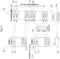
- FIGURE 2 illustrates a memory layout of memory 103, according to certain embodiments.
- Memory 103 may be viewed in logical terms as two or more panels 200 and 210 and test area 220. Each panel 200 or 210 may comprise an integer number of contiguous logical pages of memory identified as 201, 202, 211, and 212.
- Memory map 230 illustrates the mapping of logical pages to physical pages (e.g., physical pages 241-246) of memory 103. Memory map 230 may comprise unused physical pages 250 and test pages 260.
- Microcontroller 101 may further comprise address translation module 270.
- Logical pages 201, 202, 211 and 212 map to and are backed by memory in physical pages 241, 242, 245, and 246, respectively.
- Microcontroller 101 may execute instructions (and may read data) from the active panel when executing an application. If the active panel is panel 200 (i.e., PANEL1), microcontroller 101 may fetch an instruction from logical page 201, which results in a memory read from physical page 241. The fetched instruction may be a load instruction referencing an address in logical page 202. When microcontroller 101 executes the load instruction, microcontroller 101 will read the value from logical page 202, which results in a memory read from physical page 242 of memory 103. If the active panel is panel 210 (i.e., PANEL2), a fetch by microcontroller 101 from logical page 211 would result in a read from physical page 245.
- panel 200 i.e., PANEL1
- PANEL1 microcontroller 101 may fetch an instruction from logical page 201, which results in a memory read from physical page 241.
- the fetched instruction may be a load instruction referencing an address in logical page 202.
- microcontroller 101
- a portion of memory 103 may be unused resulting in one or more unused physical pages 250.
- a portion of memory 103 may contain test instructions and/or data. This test portion may be identified by logical test region 220 that maps to physical pages 260. The test portion may include routines and/or data for calibrating peripheral devices, verifying system or component operation, and debugging application code.
- address translation module 270 provides a translation of logical addressing to physical addressing.
- address translation module 270 may be a multiplexer/demultiplexer that selects one or more banks of physical memory 103 based on an indicator of the active panel.
- address translation module 270 may be a translation look-aside buffer (TLB) that provides logical to physical address translations.
- TLB translation look-aside buffer
- FIGURE 3 illustrates a memory layout of memory 103, according to certain embodiments.
- logical panels 300 and 310 map to memory 103 as illustrated in memory map 330.
- Logical panels 300 and 310 may comprise an integer number of contiguous logical pages of memory identified as 301, 302, 311, and 312.
- Memory 103 may comprise physical pages 341, 342, 343, 344.
- Memory map 330 illustrates an interleaved arrangement of logical pages.
- Logical page 301 maps to the first physical page (page 341) and logical page 302 maps to the third physical page (page 343).
- Logical page 311 maps to the second physical page (page 342) and logical page 312 maps to the fourth physical page (page 344).
- the logical pages of PANEL 1 map to the first, third, etc. physical pages while the logical pages of PANEL2 map to the second, fourth, etc. physical pages.
- FIGURE 4 illustrates a method for performing a memory swap, according to certain embodiments.
- Method 400 comprises steps 401-407, each of which is described below in more detail.
- Method 400 comprises generally serially executed steps 401, 402, 404, 405, 406, and 407 as well as parallel step 403.
- an application program may be loaded into Panel1.
- Step 401 may be performed by microcontroller 101 executing an initialization routine, for example, from test area 220.
- Step 401 may be performed by programmer 104.
- microcontroller 101 executes the application program loaded into Panel 1.
- the application program may, for example, be a motor controller program that reads inputs from peripheral devices and determines a motor control output signal based at least in part on those inputs. While microcontroller 101 executes the application program from Panel1, step 403 may be performed.
- a second application program may be loaded into Panel2.
- Step 403 may be performed by microcontroller 101 operating in a multi-processing mode.
- Step 403 may be performed by programmer 104.
- Step 403 may complete before step 404 commences to ensure that a complete program is available in Panel2 before attempting to swap panels.
- step 404 microcontroller 101 may execute one or more instructions to enable the panel swap functionality. This sequence of one or more instructions may prevent a program from accidentally swapping panels as the result of programming or compiling errors.
- step 404 involves sequentially writing two pre-determined values to a specified memory location within a pre-determined window of time.
- microcontroller 101 may execute an instruction containing an operation code (i.e., an OPCODE) specifying a panel swap operation.
- microcontroller 101 may alter a status register value to change the active panel to a previously inactive panel, e.g., Panel2 that was loaded with the second application in step 403.
- the activation of Panel2 may persist even if microcontroller 101 is subsequently reset or powered off.
- the activation of Panel2 may revert to Panel1 on the occurrence of a subsequent reset, power cycle, or execution of steps 404 and 405.
- the panel swap operation requires an operand of the logical panel number to support more than two logical memory panels.
- microcontroller 101 may determine whether the panel swap operation was successful in step 405. If yes, microcontroller 101 may proceed to execute step 407. If not, microcontroller 101 may proceed to execute step 402, thereby returning to the program in the still active panel, e.g., Panel1.
- step 405 must immediately follow the execution of step 404 to prevent accidental execution of the panel swap operation.
- a specified number of instructions may be allowed and/or required between step 405 and step 406.
- instructions may save the current register state and/or restore a previous register state.
- the panel swap operation may be used to implement a context switch allowing the use of microcontroller 101 to allow multiprocessing (e.g., virtual parallel processing).
- method 400 may be reversible such that steps 401 and 402 operate on Panel2 and steps 403 and 407 operate on Panel1.
- FIGURE 5 illustrates application source code for invoking the memory swap operation, according to certain embodiments.
- Listing 500 comprises instruction sequences 501 and 505, each stored in a different panel.
- Instruction sequence 502 may perform the steps required to enable the panel swap instruction.
- Instruction sequence 503 may perform the panel swap instruction.
- Instruction sequence 504 may branch to the entry point of instruction sequence 505 in the event that instruction sequence 503 executes successfully.
- Label 506 marks the entry point into instruction sequence 505.
- Instruction sequence 502 may be a predetermined sequence of steps designed to signal a programmer's intent to perform a panel swap. This sequence may unlock a software interlock to ensure that the panel swap sequence is not executed in error.
- microprocessor 101 executing instruction sequence 502 stores a first constant value in register W0, writes the first constant value to a specified address, stores a second constant value in register W0, and then writes the second constant value to the specified address.
- Instruction sequence 503 comprises the BOOTSWP instruction.
- Execution of the instruction sequence 503 may be subject to a software interlock. If successfully executed, microcontroller 101 may set a status flag (e.g., NVMCON.SOFTSWAP). Microcontroller 101 may also fetch instruction sequence 504 from the currently active panel before performing necessary state changes to activate a previously inactive logical panel. Once the panel swap operation is complete, microcontroller 101 may execute instruction sequence 504 to transfer program control to target 506 in instruction sequence 505. Instruction sequence 504 may be a single word program flow change instruction (PFC).
- PFC single word program flow change instruction
- microcontroller may treat the BOOTSWP instruction as a two cycle functional NOP (i.e., incrementing the program counter twice but changing no other program-accessible state). In this circumstance, microcontroller 101 may continue executing instruction sequence 501.
- the PFC target Upon a successful image swap, the PFC target will be in the newly Active panel. PFC target must be present in both code images (in case image swap fails). Code uses SOFTSWAP to determine if image swap was successful or not. When only a software swap occurs, device configuration is not refreshed since the typical reset sequence does not occur.
- Persistent boot sequence values may be changed before or after such a BOOTSWP instruction (i.e., in the original or new code image) depending upon application requirements.
- FIGURE 6 describes a status bit in a special function register, according to certain embodiments.
- This status bit labeled SOFTSWAP
- SOFTSWAP may be a readable bit that may be read as a logical '1' if memory panels have been successfully swapped using the BOOTSWP instruction.
- SOFTSWAP may be a logical '0' otherwise.
- microcontroller 101 may be configurable to operate with only one logical panel (e.g., a single boot mode).
- FIGURE 7 describes a status bit in a special function register, according to certain embodiments.
- This status bit labeled P2ACTIV, may be bit 10 of the NVMCON register. If set to logical '0', P2ACTIV may indicate that logical Panel1 is active. If set to logical '1', P2ACTIV may indicate that logical Panel2 is active.
- FIGURE 8 describes a control/status bit in a special function register, according to certain embodiments.
- This control/status bit labeled SWAPEN, may be bit 09 of the NVMCOM register.
- the SWAPEN may be a control bit in some embodiments and may require sequential writes within a predetermined window of time to be set. In certain embodiments, the SWAPEN bit must be written with a logical '1' twice in three cycles of microcontroller 101 to avoid inadvertently setting this bit.
- SWAPEN may be a dual function control/status bit.
- the SWAPEN bit may be a control bit until it is successfully set (e.g., after the second bit set operation. Once successfully set, the SWAPEN bit may become a status bit indicating whether the BOOTSWP instruction executed within the interlock window. If the BOOTSWP operation is successful, the SWAPEN bit may be cleared (and the P2ACTIV bit may be toggled). If the BOOTSWP operation was not successful, the SWAPEN bit may remain set (and the P2ACTIV bit may not be toggled). In some embodiments, the application program must clear the SWAPEN bit prior to any subsequent attempts to swap logical panels.
- microcontroller 101 is configured to operate in a single boot mode
- SOFTSWAP and P2ACTIVE may be read as a logical '0'.
- it is used as part of the interlock sequence for the BOOTSWP instruction that co-ordinates the Dual Boot Softswap operation.
- it must be written twice with a logic ' 1'.
- the second write must occur within 2 cycles of the completion of the first write to successfully set the bit. The bit will read as a logic '0' up until that point. Failure to meet write timing will reset the bit cycle count sequencer, as will clearing the bit.
- a Interlock Control register may be used to enable panel swap functionality.
- the BOOTSWP instruction may be enabled only when the interlock sequence is satisfied.
- the unlock sequence may be the same as that used to allow enable programming and/or erasure of flash memory.
- the unlock sequence may include setting the NVMCON.WR twice in quick succession.
- this software interlock requires application code to write 0x55 followed by 0xAA to the NVMKEY register where the second write must occur 2 cycles after of the completion of the first write to successfully enable the BOOTSWAP.
- Successfully meeting the write timing may open a 1 instruction cycle window during which the BOOTSWP instruction may be executed. Failure to meet the write timing may reset the NVMKEY sequencer, forcing the unlock sequence to be restarted.
- the NVMKEY register may always be read as 0.
- the NVMCON.SOFTSWAP bit may be a status bit indicating that the BOOTSWP instruction was executed within the interlock window. If the operation is successful, the NVMCON.SOFTSWAP bit may be set (and the P2ACTIV bit may be toggled). If the operation was not successful, the NVMCON.SOFTSWAP bit may retain its previous value (and the P2ACTIV bit may not be toggled).
- the NVMCON.SOFTSWAP status bit may be cleared by writing a logical '0', but it may not be set directly by application code. Application code may need to clear the NVMCON.SOFTSWAP bit prior to any subsequent Dual Boot Softswap operation attempts so that the status does not reflect a prior successful SOFTSWAP operation.
- microcontroller 101 will support an instruction with mnemonic BOOTSWP that may be executed after successful completion of an interlock sequence.
- BOOTSWP When BOOTSWP is successfully executed, microcontroller 101 may:
- the BOOTSWP instruction must be followed by a flow control instruction that targets the start of code in the (new) Active panel.
- This flow control instruction may have a side-effect of flushing the CPU pipeline. Panel swap timing will be such that the panels will swap within PS at the start of the target address pre-fetch.
- a Softswap will not reload the configuration registers, so those of the original Active panel will persist after the panel swap completes. Reloading configuration registers during a panel swap may further delay execution.
- the terms “comprises,” “comprising,” “includes,” “including,” “has,” “having,” or any other variation thereof, are intended to cover a non-exclusive inclusion.
- a process, product, article, or apparatus that comprises a list of elements is not necessarily limited only those elements but may include other elements not expressly listed or inherent to such process, process, article, or apparatus.
- "or” refers to an inclusive or and not to an exclusive or. For example, a condition A or B is satisfied by any one of the following: A is true (or present) and B is false (or not present), A is false (or not present) and B is true (or present), and both A and B are true (or present).
Landscapes
- Engineering & Computer Science (AREA)
- Software Systems (AREA)
- Theoretical Computer Science (AREA)
- General Engineering & Computer Science (AREA)
- Computer Security & Cryptography (AREA)
- Physics & Mathematics (AREA)
- General Physics & Mathematics (AREA)
- Stored Programmes (AREA)
Description
- The present disclosure relates to a dual boot panel swap mechanism, in particular a dual boot panel swap mechanism providing for a live update for a microcontroller
- Panel swap mechanisms are known from the prior art, e.g. from documents
WO 98/53619 EP 2 508 990EP 1 077 407 - According to various embodiments, a mechanism is provided to allow users to switch to a new code image without resetting the host device. Thus, the need to reset a host device may be eliminated and latency of switching to a new code image may be reduced to a few CPU cycles, for example when a firmware code update has been performed.
- According to various embodiments, such properly configured host device may allow a customer to re-flash the device and switch to a new code image without halting execution of the application. This approach may be beneficial, for example, if the host device is employed in a real-time constrained application such as a switched mode power supply (SMPS) or a motor controller. This approach also allows the peripherals to continue running while the switch is taking place. Motor-control and switch mode power supply (SMPS) applications may especially benefit from continuous execution and peripheral operation during a re-flash of the host device.
- According to various embodiments, a means is provided within a microcontroller or processor to swap two code images within a device as part of regular instruction flow and fast as possible, without a reset, and with minimal impact to exception timing.
- According to various embodiments, an inherent instruction (for example using the mnemonic BOOTSWP) is provided for a central processing unit (CPU) of a microcontroller or processor and associated mechanism to force a code image swap without the need to reset the device. According to some embodiments, the image swap may be temporary (e.g., the newly active image will not be selected after a device reset and the device will revert to the other image). According to certain embodiments, the image swap may be persistent (e.g., the newly active image will be selected after a device reset).
- According to various embodiments, a central processing unit (CPU) is provided with dual boot capabilities. The CPU comprises an instruction memory further comprising a first and second memory area, which are configured to be individually programmable. The first and second memory area are assigned to be an active memory from which instructions are executed and an inactive memory, respectively. The instruction set for the CPU comprises a dedicated instruction that performs a swap from the an active memory area to an inactive memory area, wherein the swap is performed by executing the dedicated instruction in the active memory followed by a program flow change instruction in the active memory, whereupon the inactive memory becomes the new active memory and the active memory becomes the new inactive memory and execution of instructions continues in the new active memory.
-
FIGURE 1 illustrates a microcontroller-based system, according to certain embodiments. -
FIGURE 2 illustrates a memory layout, according to certain embodiments. -
FIGURE 3 illustrates another memory layout, according to certain embodiments. -
FIGURE 4 illustrates a method of performing a memory swap, according to certain embodiments. -
FIGURE 5 illustrates application source code for invoking the memory swap operation, according to certain embodiments. -
FIGURE 6 describes a status bit in a special function register, according to certain embodiments. -
FIGURE 7 describes a status bit in a special function register, according to certain embodiments. -
FIGURE 8 describes a control/status bit in a special function register, according to certain embodiments. - The execution of a software based switch of firmware images can be challenging at the application level. This approach may be pursued in very time sensitive applications.
- Certain applications-called "Dual Boot"- need to execute from one code image (Active) while updating/re-flashing another code image (Inactive). One configuration allows for at least two separate memory areas (Panels) that may be selectively activated. In one "Dual Boot" configuration, an update to the Inactive Panel is followed by an application restart, during which time the "Dual Boot" mechanism will make the previously updated Inactive Panel become the new Active Panel. Code execution will then commence from the newly activated panel. The host device selects the Active Panel after examining a sequence number (e.g., set in nonvolatile memory). A reset sequence of this nature may require tens of milliseconds of downtime during which time the application is not executing or is at least not fully functional.
- There exists a need to re-flash/update applications with new code while continuing to execute existing application code (e.g., Dual Boot capability). Furthermore there exists a need to switch to the updated code image without the delays associated with a device reset, particularly for applications that are very time sensitive. These and other objects can be achieved by a central processing unit and method as defined in the independent claims. Further enhancements are characterized in the dependent claims.
-
FIGURE 1 illustrates microcontroller-basedsystem 100, according to certain embodiments.System 100 comprises microcontroller 101-which further comprises central processing unit (CPU) 102 and memory 103-andprogrammer 104.System 100 may be, for example, a switched mode power supply (SMPS) controller or a motor controller.Microcontroller 101 may be, for example, a model within MICROCHIP'S dsPIC/PIC24 families of microcontrollers with a processing core, one or more register files, on-board random access memory (RAM), one or more power management modes, integral analog comparator and/or analog-to-digital converter, and on-chip controllers for standard input/output protocols such as Universal Serial Bus and IEEE Std. 1149.1 (JTAG).Memory 103 may be non-volatile memory such as flash memory or electrically erasable programmable read-only memory (EEPROM).Programmer 104 may be an externally attachable computer system that provides new instructions and/or data to be stored inmemory 103.Programmer 104 may connect via a serial connection such as a universal serial bus (USB) connection. -
CPU 102 executes programs stored inmemory 103 by fetching instructions and/or data frommemory 103 and executing those instructions.CPU 102 may be, e.g., a reduced instruction set processor or a complex instruction set processor. Each instruction executed byCPU 102 may include an operation code and zero or more operands. Data and addresses may be encoded into instructions or may be retrieved from one or more registers. The result of an instruction may be stored to, e.g., a register, RAM, ormemory 103. -
Memory 103 may be randomly accessible, meaning that any unit of data can be read in a single read cycle.Memory 103 may be block accessible, meaning that a read request for a byte of data may require an internal read of a block of data, e.g., 512 bytes, into a buffer. In some embodiments, a write to an empty memory location may be immediate (e.g., within single write cycle). In some embodiments, a write to a memory location containing data may require a block erase before the write may proceed. -
FIGURE 2 illustrates a memory layout ofmemory 103, according to certain embodiments.Memory 103 may be viewed in logical terms as two ormore panels test area 220. Eachpanel Memory map 230 illustrates the mapping of logical pages to physical pages (e.g., physical pages 241-246) ofmemory 103.Memory map 230 may comprise unusedphysical pages 250 andtest pages 260.Microcontroller 101 may further compriseaddress translation module 270. -
Logical pages physical pages -
Microcontroller 101 may execute instructions (and may read data) from the active panel when executing an application. If the active panel is panel 200 (i.e., PANEL1),microcontroller 101 may fetch an instruction fromlogical page 201, which results in a memory read fromphysical page 241. The fetched instruction may be a load instruction referencing an address inlogical page 202. Whenmicrocontroller 101 executes the load instruction,microcontroller 101 will read the value fromlogical page 202, which results in a memory read fromphysical page 242 ofmemory 103. If the active panel is panel 210 (i.e., PANEL2), a fetch bymicrocontroller 101 fromlogical page 211 would result in a read fromphysical page 245. - In certain embodiments, a portion of
memory 103 may be unused resulting in one or more unusedphysical pages 250. In certain embodiments, a portion ofmemory 103 may contain test instructions and/or data. This test portion may be identified bylogical test region 220 that maps tophysical pages 260. The test portion may include routines and/or data for calibrating peripheral devices, verifying system or component operation, and debugging application code. - In certain embodiments, address
translation module 270 provides a translation of logical addressing to physical addressing. In certain embodiments, addresstranslation module 270 may be a multiplexer/demultiplexer that selects one or more banks ofphysical memory 103 based on an indicator of the active panel. In certain embodiments, addresstranslation module 270 may be a translation look-aside buffer (TLB) that provides logical to physical address translations. -
FIGURE 3 illustrates a memory layout ofmemory 103, according to certain embodiments. In the configuration ofFIG. 3 ,logical panels memory 103 as illustrated inmemory map 330.Logical panels Memory 103 may comprisephysical pages -
Memory map 330 illustrates an interleaved arrangement of logical pages.Logical page 301 maps to the first physical page (page 341) andlogical page 302 maps to the third physical page (page 343).Logical page 311 maps to the second physical page (page 342) andlogical page 312 maps to the fourth physical page (page 344). Thus, in certain embodiments the logical pages ofPANEL 1 map to the first, third, etc. physical pages while the logical pages of PANEL2 map to the second, fourth, etc. physical pages. -
FIGURE 4 illustrates a method for performing a memory swap, according to certain embodiments.Method 400 comprises steps 401-407, each of which is described below in more detail.Method 400 comprises generally serially executedsteps parallel step 403. - In
step 401, an application program may be loaded into Panel1. Step 401 may be performed bymicrocontroller 101 executing an initialization routine, for example, fromtest area 220. Step 401 may be performed byprogrammer 104. - In
step 402,microcontroller 101 executes the application program loaded intoPanel 1. The application program may, for example, be a motor controller program that reads inputs from peripheral devices and determines a motor control output signal based at least in part on those inputs. Whilemicrocontroller 101 executes the application program from Panel1, step 403 may be performed. - In
step 403, a second application program may be loaded into Panel2. Step 403 may be performed bymicrocontroller 101 operating in a multi-processing mode. Step 403 may be performed byprogrammer 104. Step 403 may complete beforestep 404 commences to ensure that a complete program is available in Panel2 before attempting to swap panels. - In
step 404,microcontroller 101 may execute one or more instructions to enable the panel swap functionality. This sequence of one or more instructions may prevent a program from accidentally swapping panels as the result of programming or compiling errors. In certain embodiments,step 404 involves sequentially writing two pre-determined values to a specified memory location within a pre-determined window of time. - In
step 405,microcontroller 101 may execute an instruction containing an operation code (i.e., an OPCODE) specifying a panel swap operation. Instep 405,microcontroller 101 may alter a status register value to change the active panel to a previously inactive panel, e.g., Panel2 that was loaded with the second application instep 403. In certain embodiments, the activation of Panel2 may persist even ifmicrocontroller 101 is subsequently reset or powered off. In certain embodiments, the activation of Panel2 may revert to Panel1 on the occurrence of a subsequent reset, power cycle, or execution ofsteps - In
step 406,microcontroller 101 may determine whether the panel swap operation was successful instep 405. If yes,microcontroller 101 may proceed to executestep 407. If not,microcontroller 101 may proceed to executestep 402, thereby returning to the program in the still active panel, e.g., Panel1. - In certain embodiments, step 405 must immediately follow the execution of
step 404 to prevent accidental execution of the panel swap operation. In certain embodiments, a specified number of instructions (or instruction cycles) may be allowed and/or required betweenstep 405 andstep 406. For example, instructions may save the current register state and/or restore a previous register state. In this way, the panel swap operation may be used to implement a context switch allowing the use ofmicrocontroller 101 to allow multiprocessing (e.g., virtual parallel processing). - In certain embodiments,
method 400 may be reversible such thatsteps -
FIGURE 5 illustrates application source code for invoking the memory swap operation, according to certain embodiments. Listing 500 comprisesinstruction sequences Instruction sequence 502 may perform the steps required to enable the panel swap instruction.Instruction sequence 503 may perform the panel swap instruction.Instruction sequence 504 may branch to the entry point ofinstruction sequence 505 in the event thatinstruction sequence 503 executes successfully.Label 506 marks the entry point intoinstruction sequence 505. -
Instruction sequence 502 may be a predetermined sequence of steps designed to signal a programmer's intent to perform a panel swap. This sequence may unlock a software interlock to ensure that the panel swap sequence is not executed in error. In certain embodiments,microprocessor 101 executinginstruction sequence 502 stores a first constant value in register W0, writes the first constant value to a specified address, stores a second constant value in register W0, and then writes the second constant value to the specified address.Instruction sequence 503 comprises the BOOTSWP instruction. - Execution of the instruction sequence 503 (e.g., the BOOTSWP instruction in certain embodiments) may be subject to a software interlock. If successfully executed,
microcontroller 101 may set a status flag (e.g., NVMCON.SOFTSWAP).Microcontroller 101 may also fetchinstruction sequence 504 from the currently active panel before performing necessary state changes to activate a previously inactive logical panel. Once the panel swap operation is complete,microcontroller 101 may executeinstruction sequence 504 to transfer program control to target 506 ininstruction sequence 505.Instruction sequence 504 may be a single word program flow change instruction (PFC). - If not successfully executed, microcontroller may treat the BOOTSWP instruction as a two cycle functional NOP (i.e., incrementing the program counter twice but changing no other program-accessible state). In this circumstance,
microcontroller 101 may continue executinginstruction sequence 501. - Upon a successful image swap, the PFC target will be in the newly Active panel. PFC target must be present in both code images (in case image swap fails). Code uses SOFTSWAP to determine if image swap was successful or not. When only a software swap occurs, device configuration is not refreshed since the typical reset sequence does not occur.
- Persistent boot sequence values may be changed before or after such a BOOTSWP instruction (i.e., in the original or new code image) depending upon application requirements.
-
FIGURE 6 describes a status bit in a special function register, according to certain embodiments. This status bit, labeled SOFTSWAP, may bebit 11 of the non-volatile memory control register, labeled NVMCON. SOFTSWAP may be a readable bit that may be read as a logical '1' if memory panels have been successfully swapped using the BOOTSWP instruction. SOFTSWAP may be a logical '0' otherwise. Incertain embodiments microcontroller 101 may be configurable to operate with only one logical panel (e.g., a single boot mode). -
FIGURE 7 describes a status bit in a special function register, according to certain embodiments. This status bit, labeled P2ACTIV, may be bit 10 of the NVMCON register. If set to logical '0', P2ACTIV may indicate that logical Panel1 is active. If set to logical '1', P2ACTIV may indicate that logical Panel2 is active. -
FIGURE 8 describes a control/status bit in a special function register, according to certain embodiments. This control/status bit, labeled SWAPEN, may be bit 09 of the NVMCOM register. The SWAPEN may be a control bit in some embodiments and may require sequential writes within a predetermined window of time to be set. In certain embodiments, the SWAPEN bit must be written with a logical '1' twice in three cycles ofmicrocontroller 101 to avoid inadvertently setting this bit. - In certain embodiments SWAPEN may be a dual function control/status bit. In one mode of operation, the SWAPEN bit may be a control bit until it is successfully set (e.g., after the second bit set operation. Once successfully set, the SWAPEN bit may become a status bit indicating whether the BOOTSWP instruction executed within the interlock window. If the BOOTSWP operation is successful, the SWAPEN bit may be cleared (and the P2ACTIV bit may be toggled). If the BOOTSWP operation was not successful, the SWAPEN bit may remain set (and the P2ACTIV bit may not be toggled). In some embodiments, the application program must clear the SWAPEN bit prior to any subsequent attempts to swap logical panels.
- Where
microcontroller 101 is configured to operate in a single boot mode, SOFTSWAP and P2ACTIVE may be read as a logical '0'. Whenmicrocontroller 101 is configured to operate in a dual moot mode, it is used as part of the interlock sequence for the BOOTSWP instruction that co-ordinates the Dual Boot Softswap operation. To help reduce the chance of inadvertently setting the SWAPEN bit, according to some embodiments it must be written twice with a logic ' 1'. According to a further embodiment, the second write must occur within 2 cycles of the completion of the first write to successfully set the bit. The bit will read as a logic '0' up until that point. Failure to meet write timing will reset the bit cycle count sequencer, as will clearing the bit. - According to certain embodiments, a Interlock Control register (NVMKEY) may be used to enable panel swap functionality. In these embodiments, the BOOTSWP instruction may be enabled only when the interlock sequence is satisfied. The unlock sequence may be the same as that used to allow enable programming and/or erasure of flash memory. The unlock sequence may include setting the NVMCON.WR twice in quick succession. In some embodiments, this software interlock requires application code to write 0x55 followed by 0xAA to the NVMKEY register where the second write must occur 2 cycles after of the completion of the first write to successfully enable the BOOTSWAP. Successfully meeting the write timing may open a 1 instruction cycle window during which the BOOTSWP instruction may be executed. Failure to meet the write timing may reset the NVMKEY sequencer, forcing the unlock sequence to be restarted. The NVMKEY register may always be read as 0.
- The NVMCON.SOFTSWAP bit may be a status bit indicating that the BOOTSWP instruction was executed within the interlock window. If the operation is successful, the NVMCON.SOFTSWAP bit may be set (and the P2ACTIV bit may be toggled). If the operation was not successful, the NVMCON.SOFTSWAP bit may retain its previous value (and the P2ACTIV bit may not be toggled). The NVMCON.SOFTSWAP status bit may be cleared by writing a logical '0', but it may not be set directly by application code. Application code may need to clear the NVMCON.SOFTSWAP bit prior to any subsequent Dual Boot Softswap operation attempts so that the status does not reflect a prior successful SOFTSWAP operation.
- In these embodiments, the following sequence may successfully unlock the BOOTSWP interlock:
-
MOV.b # 55, W0 - MOV.b WREG, NVMKEY
- MOV.b #AA, W0
- MOV.b WREG, NVMKEY
- BOOTSWP --the bootswap instruction may be executed here.
- According to some embodiments,
microcontroller 101 will support an instruction with mnemonic BOOTSWP that may be executed after successful completion of an interlock sequence. When BOOTSWP is successfully executed,microcontroller 101 may: - Switch Active and Inactive panels within the PS memory map,
- Toggle the NVMCON.P2ACTIV bit, and
- Set the NVMCON.SOFTSWAP status bit, indicating a softswap has successfully occurred.
- According to some embodiments, the BOOTSWP instruction must be followed by a flow control instruction that targets the start of code in the (new) Active panel. This flow control instruction may have a side-effect of flushing the CPU pipeline. Panel swap timing will be such that the panels will swap within PS at the start of the target address pre-fetch.
- According to some embodiments, a Softswap will not reload the configuration registers, so those of the original Active panel will persist after the panel swap completes. Reloading configuration registers during a panel swap may further delay execution.
- As used herein, the terms "comprises," "comprising," "includes," "including," "has," "having," or any other variation thereof, are intended to cover a non-exclusive inclusion. For example, a process, product, article, or apparatus that comprises a list of elements is not necessarily limited only those elements but may include other elements not expressly listed or inherent to such process, process, article, or apparatus. Further, unless expressly stated to the contrary, "or" refers to an inclusive or and not to an exclusive or. For example, a condition A or B is satisfied by any one of the following: A is true (or present) and B is false (or not present), A is false (or not present) and B is true (or present), and both A and B are true (or present).
Claims (15)
- A microcontroller (101) comprising:a central processing unit (102) having an instruction set ;an instruction memory (103) coupled with the central processing unit and comprising a first memory area (200, 300) and a second memory area (210, 310) which are configured to be individually programmable, wherein the first memory area and the second memory are are assigned to be an active memory area from which instructions are executed and an inactive memory area, respectively;wherein the instruction set for the central processing unit (102) comprises a dedicated instruction (503) having an associated opcode, wherein the dedicated instruction can only be executed after a software interlock has been unlocked by execution of an unlocking instruction sequence (502),wherein a memory area swap is performed by executing the dedicated instruction in the active memory area, whereupon the inactive memory area becomes the new active memory area and the active memory area becomes the new inactive memory area and execution of instructions continues in the new active memory area at a target (506) specified by a program flow instruction directly following the dedicated instruction in the previously active memory area.
- The microcontroller according to claim 1, wherein the program flow change instruction is a branch or jump instruction.
- The microcontroller according to claim 1, further comprising a control register comprising at least one bit which is set when said dedicated instruction has been successfully executed.
- The microcontroller according to claim 3, wherein the dedicated instruction acts as a no operation instruction when the memory area swap can not be successfully performed
- The microcontroller according to claim 1, further comprising a control register comprising at least one bit which must be set to allow a swap from the active memory area to the inactive memory area.
- The microcontroller according to claim 5, wherein the at least one bit is set by setting said bit at least twice within a predetermined time window.
- The microcontroller according to claim 6, wherein the time window is 2 instruction cycles.
- The microcontroller according to claim 1, wherein the inactive memory area is configured to be programmable while a program is executed from the active memory area.
- The microcontroller according to claim 1, wherein during initialization, the central processing unit (102) is configured to assign the first memory area to be the active memory area based at least in part on a panel select value read from nonvolatile memory.
- The microcontroller according to claim 9, wherein the panel select value in nonvolatile memory is modified as a result of successful execution of the dedicated instruction.
- The microcontroller according to claim 9, wherein the panel select value in nonvolatile memory is modifiable by a software instruction subsequent to successful execution of the dedicated instruction.
- A method for swapping a memory area in a microcontroller comprising a central processing unit (102) having an instruction set and an instruction memory (103) with a first memory area (200, 300) and a second memory area (210, 310) which are configured to be individually programmable, wherein the instruction set for the central processing unit (102) comprises a dedicated instruction (503) having an associated opcode, wherein the dedicated instruction can only be executed after a software interlock has been unlocked, the method comprising:assigning the first memory area (200, 300) to be an active memory from which instructions are executed and the second memory area (210; 310) to be an inactive memory;executing instructions from the first memory area (200; 300);executing a predefined instruction sequence (502) to unlock the software interlocl;executing the dedicated instruction, wherein the dedicated instruction when executed by the central processing unit (102) performs a memory area swap from the active memory area to the inactive memory area, whereupon the inactive memory area becomes the new active memory area and the active memory area becomes the new inactive memory area and execution of instructions continues in the new active memory area at a target (506) specified by a program flow instruction directly following the dedicated instruction in the previously active memory area.
- The method according to claim 12, further comprising setting at least one bit in a control register to allow a swap from the active memory area to the inactive memory area.
- The method according to claim 13, wherein the at least one bit is set by setting said bit at least twice within a predetermined time window.
- The method according to claim 14, wherein the time window is 2 instruction cycles.
Applications Claiming Priority (3)
| Application Number | Priority Date | Filing Date | Title |
|---|---|---|---|
| US201361780990P | 2013-03-14 | 2013-03-14 | |
| US14/204,208 US9858083B2 (en) | 2013-03-14 | 2014-03-11 | Dual boot panel SWAP mechanism |
| PCT/US2014/025329 WO2014159849A1 (en) | 2013-03-14 | 2014-03-13 | Dual boot system with memory area swapping mechanism |
Publications (2)
| Publication Number | Publication Date |
|---|---|
| EP2972823A1 EP2972823A1 (en) | 2016-01-20 |
| EP2972823B1 true EP2972823B1 (en) | 2021-04-28 |
Family
ID=51534018
Family Applications (1)
| Application Number | Title | Priority Date | Filing Date |
|---|---|---|---|
| EP14719941.8A Active EP2972823B1 (en) | 2013-03-14 | 2014-03-13 | Dual boot system with memory area swapping mechanism |
Country Status (6)
| Country | Link |
|---|---|
| US (1) | US9858083B2 (en) |
| EP (1) | EP2972823B1 (en) |
| KR (1) | KR20150129757A (en) |
| CN (1) | CN105190551B (en) |
| TW (1) | TWI617984B (en) |
| WO (1) | WO2014159849A1 (en) |
Families Citing this family (5)
| Publication number | Priority date | Publication date | Assignee | Title |
|---|---|---|---|---|
| EP3011445A4 (en) * | 2013-06-18 | 2017-02-15 | Thomson Licensing | Dual-bank telecommunication apparatus and method of upgrading firmware in dual-bank telecommunication apparatus |
| US10140109B2 (en) * | 2014-02-25 | 2018-11-27 | Ford Global Technologies, Llc | Silent in-vehicle software updates |
| US9928094B2 (en) * | 2014-11-25 | 2018-03-27 | Microsoft Technology Licensing, Llc | Hardware accelerated virtual context switching |
| CN106354524B (en) * | 2015-07-17 | 2021-01-01 | 恩智浦美国有限公司 | System and method for updating firmware in real time |
| US11513950B2 (en) | 2020-09-08 | 2022-11-29 | Western Digital Technologies, Inc. | Wear leveling in non-volatile memory |
Family Cites Families (22)
| Publication number | Priority date | Publication date | Assignee | Title |
|---|---|---|---|---|
| US6324411B1 (en) | 1997-05-20 | 2001-11-27 | Telefonaktiebolaget Lm Ericsson (Publ) | Background software loading in cellular telecommunication systems |
| US7257814B1 (en) * | 1998-12-16 | 2007-08-14 | Mips Technologies, Inc. | Method and apparatus for implementing atomicity of memory operations in dynamic multi-streaming processors |
| EP1193586A2 (en) * | 2000-09-27 | 2002-04-03 | John H. Reed, Jr. | Security system for data processing applications |
| US20020103847A1 (en) * | 2001-02-01 | 2002-08-01 | Hanan Potash | Efficient mechanism for inter-thread communication within a multi-threaded computer system |
| US20020103990A1 (en) * | 2001-02-01 | 2002-08-01 | Hanan Potash | Programmed load precession machine |
| US7856632B2 (en) * | 2004-01-29 | 2010-12-21 | Klingman Edwin E | iMEM ASCII architecture for executing system operators and processing data operators |
| US7823020B2 (en) * | 2006-08-30 | 2010-10-26 | International Business Machines Corporation | System and method for applying a destructive firmware update in a non-destructive manner |
| JP4888556B2 (en) * | 2007-06-20 | 2012-02-29 | 富士通株式会社 | Inter-unit setting synchronizer |
| CN101169728A (en) * | 2007-11-22 | 2008-04-30 | 中兴通讯股份有限公司 | Dual-boot starting device and method |
| US20120137108A1 (en) * | 2008-02-19 | 2012-05-31 | Koch Iii Kenneth Elmon | Systems and methods integrating boolean processing and memory |
| TWI411959B (en) | 2008-03-21 | 2013-10-11 | Asustek Comp Inc | Computer system with dual boot-program area and method of booting the same |
| US8775780B2 (en) * | 2009-02-27 | 2014-07-08 | Keicy Chung | System for multi-boot of a central processing unit using internal registers that direct an operating system to boot into disjoint memory spaces |
| US8554745B2 (en) * | 2009-04-27 | 2013-10-08 | Netapp, Inc. | Nearstore compression of data in a storage system |
| US20120297177A1 (en) * | 2010-11-15 | 2012-11-22 | Ghosh Anup K | Hardware Assisted Operating System Switch |
| CN102567042B (en) * | 2010-12-14 | 2015-04-15 | 国际商业机器公司 | Method and system for managing multiple software images with relocation of boot blocks |
| KR101754203B1 (en) * | 2011-01-19 | 2017-07-07 | 삼성전자주식회사 | Reconfigurable processor using power gating, complier and complie method thereof |
| CN103339604B (en) * | 2011-01-31 | 2016-10-26 | 株式会社索思未来 | Program creating device, program creating method, processor device and multicomputer system |
| JP5655677B2 (en) | 2011-04-04 | 2015-01-21 | 富士通株式会社 | Hypervisor replacement method and information processing apparatus |
| KR101844222B1 (en) * | 2011-05-27 | 2018-04-02 | 엘지전자 주식회사 | Mobile terminal and Method for controlling mode thereof |
| KR101801577B1 (en) * | 2011-06-28 | 2017-11-27 | 엘지전자 주식회사 | Mobile terminal and Method for controlling display thereof |
| US8849647B2 (en) * | 2011-10-19 | 2014-09-30 | Lsi Corporation | Dual-firmware for next generation emulation |
| KR20150128680A (en) * | 2013-03-12 | 2015-11-18 | 마이크로칩 테크놀로지 인코포레이티드 | Programmable cpu register hardware context swap mechanism |
-
2014
- 2014-03-11 US US14/204,208 patent/US9858083B2/en active Active
- 2014-03-13 CN CN201480014047.1A patent/CN105190551B/en active Active
- 2014-03-13 EP EP14719941.8A patent/EP2972823B1/en active Active
- 2014-03-13 WO PCT/US2014/025329 patent/WO2014159849A1/en not_active Ceased
- 2014-03-13 KR KR1020157027088A patent/KR20150129757A/en not_active Abandoned
- 2014-03-14 TW TW103109757A patent/TWI617984B/en active
Non-Patent Citations (1)
| Title |
|---|
| None * |
Also Published As
| Publication number | Publication date |
|---|---|
| US9858083B2 (en) | 2018-01-02 |
| KR20150129757A (en) | 2015-11-20 |
| CN105190551B (en) | 2020-06-26 |
| TWI617984B (en) | 2018-03-11 |
| WO2014159849A1 (en) | 2014-10-02 |
| EP2972823A1 (en) | 2016-01-20 |
| CN105190551A (en) | 2015-12-23 |
| US20140281465A1 (en) | 2014-09-18 |
| TW201447760A (en) | 2014-12-16 |
Similar Documents
| Publication | Publication Date | Title |
|---|---|---|
| US9733950B2 (en) | Boot sequencing for multi boot devices | |
| KR101793318B1 (en) | Instruction emulation processors, methods, and systems | |
| KR101738212B1 (en) | Instruction emulation processors, methods, and systems | |
| US10318407B2 (en) | Allocating a debug instruction set based on the current operating state in a multi-instruction-set data processing apparatus | |
| CN105144100B (en) | Central processing unit and method for performing context switching therein | |
| US20150227427A1 (en) | Restoring from a legacy os environment to a uefi pre-boot environment | |
| CN101261577A (en) | Microprocessor and method of storing data in the microprocessor | |
| US9858083B2 (en) | Dual boot panel SWAP mechanism | |
| GB2413657A (en) | Breakpoint logic unit, debug logic and breakpoint method for a data processing apparatus | |
| EP2603852B1 (en) | Alignment control | |
| KR20150139931A (en) | Mode dependent partial width load to wider register processors, methods, and systems | |
| KR20150130353A (en) | Minimizing switchover time during operating system kernel update in a hot swappable program memory | |
| US20160085559A1 (en) | Conditional Processor Auto Boot with No Boot Loader when Coupled with a Nonvolatile Memory | |
| CN114047952A (en) | Processor and method for single chip microcomputer, single chip microcomputer and storage medium | |
| JP2006221606A (en) | Data processor | |
| TW200417926A (en) | Selective interrupt suppression |
Legal Events
| Date | Code | Title | Description |
|---|---|---|---|
| PUAI | Public reference made under article 153(3) epc to a published international application that has entered the european phase |
Free format text: ORIGINAL CODE: 0009012 |
|
| 17P | Request for examination filed |
Effective date: 20151013 |
|
| AK | Designated contracting states |
Kind code of ref document: A1 Designated state(s): AL AT BE BG CH CY CZ DE DK EE ES FI FR GB GR HR HU IE IS IT LI LT LU LV MC MK MT NL NO PL PT RO RS SE SI SK SM TR |
|
| AX | Request for extension of the european patent |
Extension state: BA ME |
|
| DAX | Request for extension of the european patent (deleted) | ||
| STAA | Information on the status of an ep patent application or granted ep patent |
Free format text: STATUS: EXAMINATION IS IN PROGRESS |
|
| 17Q | First examination report despatched |
Effective date: 20190207 |
|
| REG | Reference to a national code |
Ref country code: DE Ref legal event code: R079 Ref document number: 602014076968 Country of ref document: DE Free format text: PREVIOUS MAIN CLASS: G06F0009445000 Ipc: G06F0009440100 |
|
| RIC1 | Information provided on ipc code assigned before grant |
Ipc: G06F 9/4401 20180101AFI20201015BHEP Ipc: G06F 8/656 20180101ALI20201015BHEP |
|
| GRAP | Despatch of communication of intention to grant a patent |
Free format text: ORIGINAL CODE: EPIDOSNIGR1 |
|
| STAA | Information on the status of an ep patent application or granted ep patent |
Free format text: STATUS: GRANT OF PATENT IS INTENDED |
|
| INTG | Intention to grant announced |
Effective date: 20201123 |
|
| GRAS | Grant fee paid |
Free format text: ORIGINAL CODE: EPIDOSNIGR3 |
|
| GRAA | (expected) grant |
Free format text: ORIGINAL CODE: 0009210 |
|
| STAA | Information on the status of an ep patent application or granted ep patent |
Free format text: STATUS: THE PATENT HAS BEEN GRANTED |
|
| AK | Designated contracting states |
Kind code of ref document: B1 Designated state(s): AL AT BE BG CH CY CZ DE DK EE ES FI FR GB GR HR HU IE IS IT LI LT LU LV MC MK MT NL NO PL PT RO RS SE SI SK SM TR |
|
| REG | Reference to a national code |
Ref country code: GB Ref legal event code: FG4D |
|
| REG | Reference to a national code |
Ref country code: CH Ref legal event code: EP |
|
| REG | Reference to a national code |
Ref country code: DE Ref legal event code: R096 Ref document number: 602014076968 Country of ref document: DE |
|
| REG | Reference to a national code |
Ref country code: AT Ref legal event code: REF Ref document number: 1387849 Country of ref document: AT Kind code of ref document: T Effective date: 20210515 |
|
| REG | Reference to a national code |
Ref country code: IE Ref legal event code: FG4D |
|
| REG | Reference to a national code |
Ref country code: LT Ref legal event code: MG9D |
|
| REG | Reference to a national code |
Ref country code: AT Ref legal event code: MK05 Ref document number: 1387849 Country of ref document: AT Kind code of ref document: T Effective date: 20210428 |
|
| PG25 | Lapsed in a contracting state [announced via postgrant information from national office to epo] |
Ref country code: HR Free format text: LAPSE BECAUSE OF FAILURE TO SUBMIT A TRANSLATION OF THE DESCRIPTION OR TO PAY THE FEE WITHIN THE PRESCRIBED TIME-LIMIT Effective date: 20210428 Ref country code: BG Free format text: LAPSE BECAUSE OF FAILURE TO SUBMIT A TRANSLATION OF THE DESCRIPTION OR TO PAY THE FEE WITHIN THE PRESCRIBED TIME-LIMIT Effective date: 20210728 Ref country code: AT Free format text: LAPSE BECAUSE OF FAILURE TO SUBMIT A TRANSLATION OF THE DESCRIPTION OR TO PAY THE FEE WITHIN THE PRESCRIBED TIME-LIMIT Effective date: 20210428 Ref country code: FI Free format text: LAPSE BECAUSE OF FAILURE TO SUBMIT A TRANSLATION OF THE DESCRIPTION OR TO PAY THE FEE WITHIN THE PRESCRIBED TIME-LIMIT Effective date: 20210428 Ref country code: NL Free format text: LAPSE BECAUSE OF FAILURE TO SUBMIT A TRANSLATION OF THE DESCRIPTION OR TO PAY THE FEE WITHIN THE PRESCRIBED TIME-LIMIT Effective date: 20210428 Ref country code: LT Free format text: LAPSE BECAUSE OF FAILURE TO SUBMIT A TRANSLATION OF THE DESCRIPTION OR TO PAY THE FEE WITHIN THE PRESCRIBED TIME-LIMIT Effective date: 20210428 |
|
| PG25 | Lapsed in a contracting state [announced via postgrant information from national office to epo] |
Ref country code: LV Free format text: LAPSE BECAUSE OF FAILURE TO SUBMIT A TRANSLATION OF THE DESCRIPTION OR TO PAY THE FEE WITHIN THE PRESCRIBED TIME-LIMIT Effective date: 20210428 Ref country code: GR Free format text: LAPSE BECAUSE OF FAILURE TO SUBMIT A TRANSLATION OF THE DESCRIPTION OR TO PAY THE FEE WITHIN THE PRESCRIBED TIME-LIMIT Effective date: 20210729 Ref country code: IS Free format text: LAPSE BECAUSE OF FAILURE TO SUBMIT A TRANSLATION OF THE DESCRIPTION OR TO PAY THE FEE WITHIN THE PRESCRIBED TIME-LIMIT Effective date: 20210828 Ref country code: RS Free format text: LAPSE BECAUSE OF FAILURE TO SUBMIT A TRANSLATION OF THE DESCRIPTION OR TO PAY THE FEE WITHIN THE PRESCRIBED TIME-LIMIT Effective date: 20210428 Ref country code: SE Free format text: LAPSE BECAUSE OF FAILURE TO SUBMIT A TRANSLATION OF THE DESCRIPTION OR TO PAY THE FEE WITHIN THE PRESCRIBED TIME-LIMIT Effective date: 20210428 Ref country code: PT Free format text: LAPSE BECAUSE OF FAILURE TO SUBMIT A TRANSLATION OF THE DESCRIPTION OR TO PAY THE FEE WITHIN THE PRESCRIBED TIME-LIMIT Effective date: 20210830 Ref country code: PL Free format text: LAPSE BECAUSE OF FAILURE TO SUBMIT A TRANSLATION OF THE DESCRIPTION OR TO PAY THE FEE WITHIN THE PRESCRIBED TIME-LIMIT Effective date: 20210428 Ref country code: NO Free format text: LAPSE BECAUSE OF FAILURE TO SUBMIT A TRANSLATION OF THE DESCRIPTION OR TO PAY THE FEE WITHIN THE PRESCRIBED TIME-LIMIT Effective date: 20210728 Ref country code: ES Free format text: LAPSE BECAUSE OF FAILURE TO SUBMIT A TRANSLATION OF THE DESCRIPTION OR TO PAY THE FEE WITHIN THE PRESCRIBED TIME-LIMIT Effective date: 20210428 |
|
| REG | Reference to a national code |
Ref country code: NL Ref legal event code: MP Effective date: 20210428 |
|
| PG25 | Lapsed in a contracting state [announced via postgrant information from national office to epo] |
Ref country code: CZ Free format text: LAPSE BECAUSE OF FAILURE TO SUBMIT A TRANSLATION OF THE DESCRIPTION OR TO PAY THE FEE WITHIN THE PRESCRIBED TIME-LIMIT Effective date: 20210428 Ref country code: DK Free format text: LAPSE BECAUSE OF FAILURE TO SUBMIT A TRANSLATION OF THE DESCRIPTION OR TO PAY THE FEE WITHIN THE PRESCRIBED TIME-LIMIT Effective date: 20210428 Ref country code: EE Free format text: LAPSE BECAUSE OF FAILURE TO SUBMIT A TRANSLATION OF THE DESCRIPTION OR TO PAY THE FEE WITHIN THE PRESCRIBED TIME-LIMIT Effective date: 20210428 Ref country code: SM Free format text: LAPSE BECAUSE OF FAILURE TO SUBMIT A TRANSLATION OF THE DESCRIPTION OR TO PAY THE FEE WITHIN THE PRESCRIBED TIME-LIMIT Effective date: 20210428 Ref country code: SK Free format text: LAPSE BECAUSE OF FAILURE TO SUBMIT A TRANSLATION OF THE DESCRIPTION OR TO PAY THE FEE WITHIN THE PRESCRIBED TIME-LIMIT Effective date: 20210428 Ref country code: RO Free format text: LAPSE BECAUSE OF FAILURE TO SUBMIT A TRANSLATION OF THE DESCRIPTION OR TO PAY THE FEE WITHIN THE PRESCRIBED TIME-LIMIT Effective date: 20210428 |
|
| REG | Reference to a national code |
Ref country code: DE Ref legal event code: R097 Ref document number: 602014076968 Country of ref document: DE |
|
| PLBE | No opposition filed within time limit |
Free format text: ORIGINAL CODE: 0009261 |
|
| STAA | Information on the status of an ep patent application or granted ep patent |
Free format text: STATUS: NO OPPOSITION FILED WITHIN TIME LIMIT |
|
| 26N | No opposition filed |
Effective date: 20220131 |
|
| PG25 | Lapsed in a contracting state [announced via postgrant information from national office to epo] |
Ref country code: IS Free format text: LAPSE BECAUSE OF FAILURE TO SUBMIT A TRANSLATION OF THE DESCRIPTION OR TO PAY THE FEE WITHIN THE PRESCRIBED TIME-LIMIT Effective date: 20210828 Ref country code: AL Free format text: LAPSE BECAUSE OF FAILURE TO SUBMIT A TRANSLATION OF THE DESCRIPTION OR TO PAY THE FEE WITHIN THE PRESCRIBED TIME-LIMIT Effective date: 20210428 |
|
| PG25 | Lapsed in a contracting state [announced via postgrant information from national office to epo] |
Ref country code: IT Free format text: LAPSE BECAUSE OF FAILURE TO SUBMIT A TRANSLATION OF THE DESCRIPTION OR TO PAY THE FEE WITHIN THE PRESCRIBED TIME-LIMIT Effective date: 20210428 |
|
| PG25 | Lapsed in a contracting state [announced via postgrant information from national office to epo] |
Ref country code: MC Free format text: LAPSE BECAUSE OF FAILURE TO SUBMIT A TRANSLATION OF THE DESCRIPTION OR TO PAY THE FEE WITHIN THE PRESCRIBED TIME-LIMIT Effective date: 20210428 |
|
| REG | Reference to a national code |
Ref country code: CH Ref legal event code: PL |
|
| GBPC | Gb: european patent ceased through non-payment of renewal fee |
Effective date: 20220313 |
|
| REG | Reference to a national code |
Ref country code: BE Ref legal event code: MM Effective date: 20220331 |
|
| PG25 | Lapsed in a contracting state [announced via postgrant information from national office to epo] |
Ref country code: LU Free format text: LAPSE BECAUSE OF NON-PAYMENT OF DUE FEES Effective date: 20220313 Ref country code: LI Free format text: LAPSE BECAUSE OF NON-PAYMENT OF DUE FEES Effective date: 20220331 Ref country code: IE Free format text: LAPSE BECAUSE OF NON-PAYMENT OF DUE FEES Effective date: 20220313 Ref country code: GB Free format text: LAPSE BECAUSE OF NON-PAYMENT OF DUE FEES Effective date: 20220313 Ref country code: FR Free format text: LAPSE BECAUSE OF NON-PAYMENT OF DUE FEES Effective date: 20220331 Ref country code: CH Free format text: LAPSE BECAUSE OF NON-PAYMENT OF DUE FEES Effective date: 20220331 |
|
| PG25 | Lapsed in a contracting state [announced via postgrant information from national office to epo] |
Ref country code: BE Free format text: LAPSE BECAUSE OF NON-PAYMENT OF DUE FEES Effective date: 20220331 |
|
| P01 | Opt-out of the competence of the unified patent court (upc) registered |
Effective date: 20230528 |
|
| PG25 | Lapsed in a contracting state [announced via postgrant information from national office to epo] |
Ref country code: HU Free format text: LAPSE BECAUSE OF FAILURE TO SUBMIT A TRANSLATION OF THE DESCRIPTION OR TO PAY THE FEE WITHIN THE PRESCRIBED TIME-LIMIT; INVALID AB INITIO Effective date: 20140313 |
|
| PG25 | Lapsed in a contracting state [announced via postgrant information from national office to epo] |
Ref country code: MK Free format text: LAPSE BECAUSE OF FAILURE TO SUBMIT A TRANSLATION OF THE DESCRIPTION OR TO PAY THE FEE WITHIN THE PRESCRIBED TIME-LIMIT Effective date: 20210428 Ref country code: CY Free format text: LAPSE BECAUSE OF FAILURE TO SUBMIT A TRANSLATION OF THE DESCRIPTION OR TO PAY THE FEE WITHIN THE PRESCRIBED TIME-LIMIT Effective date: 20210428 |
|
| PG25 | Lapsed in a contracting state [announced via postgrant information from national office to epo] |
Ref country code: TR Free format text: LAPSE BECAUSE OF FAILURE TO SUBMIT A TRANSLATION OF THE DESCRIPTION OR TO PAY THE FEE WITHIN THE PRESCRIBED TIME-LIMIT Effective date: 20210428 |
|
| PG25 | Lapsed in a contracting state [announced via postgrant information from national office to epo] |
Ref country code: MT Free format text: LAPSE BECAUSE OF FAILURE TO SUBMIT A TRANSLATION OF THE DESCRIPTION OR TO PAY THE FEE WITHIN THE PRESCRIBED TIME-LIMIT Effective date: 20210428 |
|
| PGFP | Annual fee paid to national office [announced via postgrant information from national office to epo] |
Ref country code: DE Payment date: 20260219 Year of fee payment: 13 |