EP2972787B1 - Eliminating redundant synchronization barriers in instruction processing circuits, and related processor systems, methods, and computer-readable media - Google Patents
Eliminating redundant synchronization barriers in instruction processing circuits, and related processor systems, methods, and computer-readable media Download PDFInfo
- Publication number
- EP2972787B1 EP2972787B1 EP14719128.2A EP14719128A EP2972787B1 EP 2972787 B1 EP2972787 B1 EP 2972787B1 EP 14719128 A EP14719128 A EP 14719128A EP 2972787 B1 EP2972787 B1 EP 2972787B1
- Authority
- EP
- European Patent Office
- Prior art keywords
- instruction
- synchronization
- event
- synchronization event
- barrier
- Prior art date
- Legal status (The legal status is an assumption and is not a legal conclusion. Google has not performed a legal analysis and makes no representation as to the accuracy of the status listed.)
- Not-in-force
Links
Images


Classifications
-
- G—PHYSICS
- G06—COMPUTING; CALCULATING OR COUNTING
- G06F—ELECTRIC DIGITAL DATA PROCESSING
- G06F9/00—Arrangements for program control, e.g. control units
- G06F9/06—Arrangements for program control, e.g. control units using stored programs, i.e. using an internal store of processing equipment to receive or retain programs
- G06F9/30—Arrangements for executing machine instructions, e.g. instruction decode
- G06F9/30003—Arrangements for executing specific machine instructions
- G06F9/30076—Arrangements for executing specific machine instructions to perform miscellaneous control operations, e.g. NOP
- G06F9/30087—Synchronisation or serialisation instructions
Definitions
- the technology of the disclosure relates to processing of pipelined computer instructions in central processing unit (CPU)-based systems.
- CPU central processing unit
- Instruction pipelining is a processing technique whereby a throughput of computer instructions being processed by a CPU may be increased by splitting the processing of each instruction into a series of steps.
- the instructions are executed in an "execution pipeline" composed of multiple stages, with each stage carrying out one of the steps for each of a series of instructions.
- execution pipeline composed of multiple stages, with each stage carrying out one of the steps for each of a series of instructions.
- steps for multiple instructions can be evaluated in parallel.
- a CPU may employ multiple execution pipelines to further boost performance.
- Some computer architectures that implement instruction pipelining may permit processor optimizations, such as speculative data reads and out-of-order execution of program instructions. While providing further CPU performance improvement, these optimizations may lead to unintended and/or undesirable program behavior if, for example, the executing program depends on data being accessed or instructions being executed in a specified order.
- an executing instruction may effect a change in a state of the CPU that must be successfully completed before subsequent instructions are allowed to execute.
- a change in a state of the CPU may include changes that affect how the subsequent instructions access resources, such as a change in processor mode or a modification of a page table.
- a "synchronization barrier” may be used in software to ensure that a prior operation (i.e., a data access or instruction execution) completes before code execution is permitted to continue.
- a synchronization barrier may be expressly provided by an instruction, such as the ARM architecture ISB (instruction synchronization barrier) instruction, or may be implemented as part of another instruction or operation.
- a computer's architecture may provide that specific operations requiring a synchronization barrier may have the synchronization automatically handled by the computer's hardware, while other operations require software to expressly include a synchronization barrier. Note however, that for scenarios in which a software synchronization barrier is present, the software synchronization barrier may prove redundant if another synchronization operation occurs immediately prior to execution of the software synchronization barrier.
- US 2011/145512 discloses a method for eliminating redundant synchronization barriers.
- Embodiments of the disclosure include eliminating redundant synchronization barriers from execution pipelines in instruction processing circuits, and related processor systems, methods, and computer-readable media.
- a computer's architecture may require that a software synchronization barrier be employed, even though a synchronization operation may also occur immediately prior to execution of the software synchronization barrier.
- a software synchronization barrier By tracking the occurrence of synchronization events, unnecessary software synchronization barriers may be identified and eliminated, thus improving performance of a central processing unit (CPU).
- CPU central processing unit
- a method for eliminating redundant synchronization barriers in an instruction stream comprises detecting a first synchronization event.
- the method further comprises detecting a next instruction in an instruction stream.
- the method additionally comprises determining whether the next instruction comprises a synchronization barrier of a type corresponding to the first synchronization event.
- the method also comprises eliminating the next instruction from the instruction stream, responsive to determining that the next instruction comprises a synchronization barrier of a type corresponding to the first synchronization event. In this manner, the average number of instructions executed during each clock cycle by the CPU may be increased by avoiding unnecessary synchronization operations.
- an instruction processing circuit comprises a synchronization event detection circuit and an optimization circuit.
- the synchronization event detection circuit is configured to detect a first synchronization event.
- the optimization circuit is configured to detect a next instruction in an instruction stream, and determine whether the next instruction comprises a synchronization barrier of a type corresponding to the first synchronization event.
- the optimization circuit is further configured to eliminate the next instruction from the instruction stream, responsive to determining that the next instruction comprises a synchronization barrier of a type corresponding to the first synchronization event.
- an instruction processing circuit comprises a means for detecting a first synchronization event.
- the instruction processing circuit further comprises a means for detecting a next instruction in an instruction stream.
- the instruction processing circuit additionally comprises a means for determining whether the next instruction comprises a synchronization barrier of a type corresponding to the first synchronization event.
- the instruction processing circuit also comprises a means for eliminating the next instruction from the instruction stream, responsive to determining that the next instruction comprises a synchronization barrier of a type corresponding to the first synchronization event.
- a non-transitory computer-readable medium having stored thereon computer-executable instructions to cause a processor to implement a method.
- the method implemented by the computer-executable instructions comprises detecting a first synchronization event.
- the method implemented by the computer-executable instructions further comprises detecting a next instruction in an instruction stream.
- the method implemented by the computer-executable instructions additionally comprises determining whether the next instruction comprises a synchronization barrier of a type corresponding to the first synchronization event.
- the method implemented by the computer-executable instructions also comprises eliminating the next instruction from the instruction stream, responsive to determining that the next instruction comprises a synchronization barrier of a type corresponding to the first synchronization event.
- Embodiments of the disclosure include eliminating redundant synchronization barriers from execution pipelines in instruction processing circuits, and related processor systems, methods, and computer-readable media.
- a computer's architecture may require that a software synchronization barrier be employed, even though a synchronization operation may also occur immediately prior to execution of the software synchronization barrier.
- a software synchronization barrier By tracking the occurrence of synchronization events, unnecessary software synchronization barriers may be identified and eliminated, thus improving performance of a central processing unit (CPU).
- CPU central processing unit
- a method for eliminating redundant synchronization barriers in an instruction stream comprises detecting a first synchronization event.
- the method further comprises detecting a next instruction in an instruction stream.
- the method additionally comprises determining whether the next instruction comprises a synchronization barrier of a type corresponding to the first synchronization event.
- the method also comprises eliminating the next instruction from the instruction stream, responsive to determining that the next instruction comprises a synchronization barrier of a type corresponding to the first synchronization event. In this manner, the average number of instructions executed during each clock cycle by the CPU may be increased by avoiding unnecessary synchronization operations.
- Figure 1 is a block diagram of an exemplary processor-based system 10 for retrieving and processing computer instructions to be placed into one or more execution pipelines 12(0)-12(Q).
- the processor-based system 10 provides an instruction processing circuit 14 that is configured to detect and eliminate redundant synchronization barriers.
- an "instruction" may refer to a combination of bits defined by an instruction set architecture that direct a computer processor to carry out a specified task or tasks.
- an instruction may indicate operations for reading data from and/or writing data to registers 16(0)-16(M), which provide local storage accessible by the processor-based system 10.
- Exemplary instruction set architectures include, but are not limited to, ARM, Thumb, and A64 architectures.
- instructions are processed in the processor-based system 10 in a continuous flow represented by an instruction stream 18.
- the instruction stream 18 may be continuously processed as the processor-based system 10 is operating and executing the instructions.
- the instruction stream 18 begins with an instruction memory 20, which provides persistent storage for instructions in a computer-executable program.
- An instruction fetch circuit 22 reads an instruction represented by arrow 24 (hereinafter "instruction 24") from the instruction memory 20 and/or optionally from an instruction cache 26.
- the instruction fetch circuit 22 may increment a program counter (not shown), which may be stored in one of the registers 16(0)-16(M).
- the instruction 24 proceeds to an instruction decode circuit 28 that translates the instruction into processor-specific microinstructions.
- the instruction decode circuit 28 stores a group of multiple instructions 30(0)-30(N) simultaneously for decoding.
- the instructions 30(0)-30(N) After the instructions 30(0)-30(N) have been fetched and decoded, they are optionally issued to an instruction queue 32 as a buffer for storing the instructions 30(0)-30(N). The instructions 30(0)-30(N) are then issued to one of the execution pipelines 12(0)-12(Q) for execution.
- the execution pipelines 12(0)-12(Q) may restrict the types of operations that may be carried out by instructions that execute within the execution pipelines 12(0)-12(Q). For example, pipeline P 0 may not permit read access to the registers 16(0)-16(M); accordingly, an instruction that indicates an operation to read register R 0 may only be issued to one of the execution pipelines P 1 through P Q .
- the instruction processing circuit 14 may be any type of device or circuit, and may be implemented or performed with a processor, a digital signal processor (DSP), an Application Specific Integrated Circuit (ASIC), a field-programmable gate array (FPGA) or other programmable logic device, discrete gate or transistor logic, discrete hardware components, or any combination thereof designed to perform the functions described herein. In some embodiments, the instruction processing circuit 14 is incorporated into the instruction decode circuit 28.
- DSP digital signal processor
- ASIC Application Specific Integrated Circuit
- FPGA field-programmable gate array
- the instruction processing circuit 14 in this example is configured to detect and eliminate redundant synchronization barriers in the instruction stream 18.
- the instruction processing circuit 14 may employ a synchronization event detection circuit 34 configured to detect a synchronization event.
- the instruction processing circuit 14 may also employ an optimization circuit 36 configured to detect a next instruction indicating a redundant synchronization barrier of a type corresponding to the synchronization event.
- the optimization circuit 36 may be further configured to eliminate the next instruction from the instruction stream 18.
- the instruction processing circuit 14 may utilize a synchronization flag 38 to indicate an occurrence of a synchronization event and determine whether a redundant synchronization barrier has been detected.
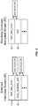
- Figure 2 illustrates the instruction processing circuit 14 of Figure 1 detecting a synchronization event, and subsequently detecting a redundant synchronization barrier.
- a detected instruction stream 40 represents a series of instructions fetched in the instruction stream 18 and detected by the instruction processing circuit 14.
- First in the detected instruction stream 40 is an INST_REQ_SYNC instruction 42.
- the INST_REQ_SYNC instruction 42 may be any instruction indicating an operation for which the computer architecture requires software to expressly include a subsequent synchronization barrier, and for which the computer hardware is also permitted to perform a synchronization operation.
- the computer hardware carries out a synchronization operation in response to the INST_REQ_SYNC instruction 42, resulting in a synchronization event 44 being detected by the instruction processing circuit 14.
- the synchronization event 44 may be a data synchronization operation, while some embodiments may provide that the synchronization event 44 is an instruction synchronization operation.
- a SYNC_BARRIER_INST instruction 46 is detected next in the detected instruction stream 40 by the instruction processing circuit 14.
- the SYNC_BARRIER_INST instruction 46 is a synchronization barrier instruction that causes a synchronization event 48 to occur.
- the synchronization event 48 triggered by the SYNC_BARRIER_INST instruction 46 is of the same type as the synchronization event 44.
- the "type" of a synchronization event refers to a general categorization of the synchronization event as, for example, a data synchronization operation or an instruction synchronization operation.
- a synchronization event may be considered a "full" synchronization event if it ensures barrier operations for both read and write operations, and applies to both inner- and outer-cacheable memory systems and both shareable and non-shareable memory.
- the synchronization event may be more limited in scope in that it ensures barrier operations only in narrow circumstances than a full synchronization event.
- a synchronization event may be considered of the same type as a preceding synchronization event if the synchronization event belongs to the same general categorization and is of a same or narrower scope as the preceding synchronization event.
- a resulting optimized instruction stream 50 illustrates one exemplary result of the process described above.
- the resulting optimized instruction stream 50 includes an INSTR_REQ_SYNC instruction 52 corresponding to the INSTR_REQ_SYNC instruction 42.
- the INST_REQ_SYNC instruction 52 is an instruction indicating an operation to be followed by a software synchronization barrier, and for which the computer hardware is also permitted to perform a synchronization operation.
- the computer hardware carries out a synchronization operation in response to the INST_REQ_SYNC instruction 52, resulting in a synchronization event 54.
- the synchronization event 54 may be a data synchronization operation, while some embodiments may provide that the synchronization event 54 is an instruction synchronization operation.
- the SYNC_BARRIER_INST instruction 46 has been replaced in the resulting optimized instruction stream 50 with an NOP (no operation) instruction 56. Consequently, there is no redundant synchronization event immediately following the synchronization event 54, resulting in improved CPU performance and instruction throughput.
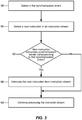
- Figure 3 is provided to illustrate an exemplary process for detecting and eliminating a redundant synchronization barrier, with additional reference to Figures 1 and 2 .
- the exemplary process begins with the instruction processing circuit 14 detecting a first synchronization event, such as the synchronization event 44 of Figure 2 (block 58).
- the first synchronization event may be a data synchronization operation, while some embodiments may provide that the first synchronization event is an instruction synchronization operation.
- the first synchronization event may result from the execution of an instruction, or may be caused by an unrelated operation such as an interrupt or an exception return.
- the instruction processing circuit 14 detects a next instruction in an instruction stream (block 60).
- the instruction processing circuit 14 determines whether the next instruction comprises a synchronization barrier of a type corresponding to the first synchronization event (block 62). For example, the instruction processing circuit 14 determines whether the first synchronization event and the next instruction are both considered data synchronization operations, or whether both are instruction synchronization operations. If the next instruction does not comprise a synchronization barrier of a type corresponding to the first synchronization event, processing of the instruction stream continues at block 64 of Figure 3 . If the next instruction does comprise a synchronization barrier corresponding to the first synchronization event, the instruction processing circuit 14 eliminates the next instruction from the instruction stream (block 66). In some embodiments, eliminating the next instruction may include replacing the next instruction with an NOP instruction, while some embodiments may provide that eliminating the next instruction comprises removing the next instruction from the instruction stream. Processing of the instruction stream 18 then continues at block 64.
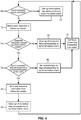
- Figure 4 is a flowchart illustrating a more detailed exemplary process of an instruction processing circuit, such as the instruction processing circuit 14 of Figure 1 , for eliminating redundant synchronization barriers.
- the exemplary process illustrated in Figure 4 begins with the instruction processing circuit determining whether a synchronization event has been detected (block 68).
- the synchronization event may be a data synchronization operation, while some embodiments may provide that the synchronization event is an instruction synchronization operation.
- a synchronization event may result from execution of an instruction, or may arise from an unrelated operation such as an interrupt or an exception return. Accordingly, detection of a synchronization event may be made by detecting an effect of the synchronization event, such as a pipeline flush, and/or by comparing a detected instruction to a list of instructions known to trigger a synchronization event.
- a synchronization flag corresponding to a type of the synchronization event (e.g., data synchronization or instruction synchronization) is set (block 70).
- the synchronization flag indicates whether a synchronization event occurred immediately prior to execution of a next instruction. Some embodiments may provide that the synchronization flag indicates the occurrence of a data synchronization event, while in some embodiments the synchronization flag corresponds to an occurrence of an instruction synchronization event. Processing then resumes at block 72 of Figure 4 . If no synchronization event is detected at block 68, processing returns to block 72.
- the instruction processing circuit then detects a next instruction in an instruction stream, such as the instruction stream 18 (block 72).
- the instruction processing circuit determines whether a synchronization event, for example the synchronization event 44 of Figure 2 , is caused by the detected instruction (block 74).
- the synchronization event may be a data synchronization operation, while some embodiments may provide that the synchronization event is an instruction synchronization operation.
- the instruction processing circuit determines at block 74 of Figure 4 that the detected instruction does not cause a synchronization event, the instruction processing circuit clears the synchronization flag that corresponds to a type of synchronization event (e.g., data synchronization or instruction synchronization) (block 75) if it was set previously (for example, in block 70), and continues processing of the detected instruction continues (block 76). The instruction processing circuit then returns to block 68. If the instruction processing circuit determines at block 74 that a synchronization event is caused by the detected instruction, the instruction processing circuit next evaluates whether the detected instruction is a redundant synchronization barrier.
- a type of synchronization event e.g., data synchronization or instruction synchronization
- the instruction processing circuit examines whether the synchronization flag corresponding to the type of the synchronization event (e.g., data synchronization or instruction synchronization) is set (block 78). If the synchronization flag is not set, then a synchronization event of appropriate type and scope did not occur immediately prior to the detected instruction, and therefore the detected instruction is not a redundant synchronization barrier. Accordingly, the synchronization flag is set to indicate that a synchronization event was caused by the detected instruction (block 80), and processing of the detected instruction continues at block 76. Afterwards, the instruction processing circuit returns to block 68.
- the synchronization flag corresponding to the type of the synchronization event (e.g., data synchronization or instruction synchronization) is set (block 78). If the synchronization flag is not set, then a synchronization event of appropriate type and scope did not occur immediately prior to the detected instruction, and therefore the detected instruction is not a redundant synchronization barrier. Accordingly, the synchronization flag is set to indicate that a synchronization
- the instruction processing circuit determines that the synchronization flag corresponding to the synchronization event is set, the detected instruction has been identified as a redundant synchronization barrier.
- the instruction processing circuit thus eliminates the detected instruction from the instruction stream (block 82).
- the instruction processing circuit may eliminate the detected instruction by replacing the detected instruction with an NOP instruction, such as the NOP instruction 56 of Figure 2 , in the instruction stream, while some embodiments may provide that the detected instruction is removed entirely from the instruction stream. It is to be understood that, in some embodiments, the occurrence of more than two consecutive instructions resulting in synchronization events of the same type may be unlikely.
- the instruction processing circuit may clear the synchronization flag corresponding to the synchronization event upon eliminating the detected instruction from the instruction stream (block 83).
- the operations of block 83 may be omitted.
- operations for detecting the detected instruction and the synchronization event may be carried out by, for example, the synchronization event detection circuit 34 of the instruction processing circuit 14 of Figure 1 . It is to be further understood that operations for detecting and eliminating a redundant synchronization barrier may be carried out by, for example, the optimization circuit 36 of the instruction processing circuit 14 of Figure 1 .
- a detected instruction stream 84 represents a series of instructions fetched in the instruction stream 18 and detected by the instruction processing circuit 14.
- First in the detected instruction stream 84 is an ARM architecture MCR ("Move to coprocessor from ARM register(s)") instruction 86.
- the MCR instruction 86 is an instruction indicating an operation to write a value to translation table base register 0 (TTBR0), which, in a computer employing the ARM architecture, stores a physical address of a translation table.
- TTBR0 translation table base register 0
- the ARM architecture requires that the MCR instruction 86 be followed by a software instruction synchronization operation.
- the computer hardware may also be permitted to perform an instruction synchronization operation after execution of the MCR instruction 86. Accordingly, in this example, the computer hardware automatically initiates a synchronization operation in response to execution of the MCR instruction 86, resulting in a synchronization event 88.
- an ARM architecture ISB instruction synchronization barrier
- the ISB instruction 90 is a synchronization barrier instruction that causes a synchronization event 92 to occur.
- the synchronization event 92 triggered by the ISB instruction 90 is of the same type (i.e., an instruction synchronization operation having the same or narrower scope) as the synchronization event 88. Note that because no other instruction executes after the synchronization event 88 and before the synchronization event 92, the synchronization event 92, and the ISB instruction 90 that triggered it, are redundant and may be eliminated by the instruction processing circuit 14.
- a resulting optimized instruction stream 94 illustrates one exemplary result.
- the resulting optimized instruction stream 94 includes an MCR instruction 96 corresponding to the MCR instruction 86.
- the computer hardware carries out an instruction synchronization operation, resulting in a synchronization event 98.
- the ISB instruction 90 has been replaced in this instance by an NOP instruction 100 in the resulting optimized instruction stream 94.
- NOP instruction 100 there is no redundant synchronization event immediately following the synchronization event 98, resulting in improved CPU performance and instruction throughput.
- a redundant synchronization barrier may be eliminated from the instruction stream 18 by the instruction processing circuit 14 of Figure 1 .
- the instruction processing circuit 14 may eliminate the redundant synchronization barrier by replacing it with an NOP instruction indicating no operation, or by removing it entirely from the instruction stream 18.
- the instruction processing circuit 14 may process a given detected instruction stream into different resulting instruction streams.
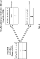
- Figure 6 shows an exemplary detected instruction stream 102 including a redundant synchronization barrier, and corresponding resulting optimized instruction stream examples 104(1) and 104(2) that may be generated by the instruction processing circuit 14.
- the detected instruction stream 102 includes two ARM architecture instructions: an MCR instruction that indicates an operation to write a value to TTBR0, followed by an ISB synchronization barrier instruction that triggers an instruction synchronization event.
- Resulting optimized instruction stream examples 104 illustrate exemplary sequences of instructions into which the instructions in the detected instruction stream 102 may be processed by the instruction processing circuit 14 of Figure 1 .
- the ISB instruction in the detected instruction stream 102 may be replaced with an instruction indicating no operation (i.e., NOP).
- NOP instruction indicating no operation
- exemplary instruction stream 104(1) comprises the MCR instruction followed by an NOP instruction.
- some embodiments described herein provide that the ISB instruction in the detected instruction stream 102 will be removed entirely from the instruction stream 18. Accordingly, instruction stream 104(2) comprises only the MCR instruction.
- a synchronization event preceding a software synchronization barrier may result from operations unrelated to instruction execution, such as an interrupt or an exception return.
- Figure 7 illustrates optimization of an exemplary instruction stream containing a redundant synchronization barrier.
- a detected instruction stream 106 represents a series of instructions fetched in the instruction stream 18 and detected by the instruction processing circuit 14 of Figure 1 .
- a synchronization event 108 occurs in response to an operation such as an interrupt or an exception return.
- an ARM architecture ISB instruction 110 is detected in the detected instruction stream 106.
- the ISB instruction 110 is a synchronization barrier instruction that causes a synchronization event 112 to occur.
- the synchronization event 112 triggered by the ISB instruction 110 is of the same type (i.e., an instruction synchronization operation having the same or narrower scope) as the synchronization event 108. Note that because no other instruction executes after the synchronization event 108 and before the synchronization event 112, the synchronization event 112, and the ISB instruction 110 that triggered it, are redundant and may be eliminated by the instruction processing circuit 14.
- a resulting optimized instruction stream 114 illustrates one exemplary result.
- a synchronization event 116 occurs in response to an operation such as an interrupt or an exception return.
- the ISB instruction 110 has been replaced in this instance by an NOP instruction 118 in the resulting optimized instruction stream 114.
- NOP instruction 118 there is no redundant synchronization event immediately following the synchronization event 116, resulting in improved CPU performance and instruction throughput.
- Eliminating redundant synchronization barriers from execution pipelines in instruction processing circuits, and related processor systems, methods, and computer-readable media according to embodiments disclosed herein may be provided in or integrated into any processor-based device. Examples, without limitation, include a set top box, an entertainment unit, a navigation device, a communications device, a fixed location data unit, a mobile location data unit, a mobile phone, a cellular phone, a computer, a portable computer, a desktop computer, a personal digital assistant (PDA), a monitor, a computer monitor, a television, a tuner, a radio, a satellite radio, a music player, a digital music player, a portable music player, a digital video player, a video player, a digital video disc (DVD) player, and a portable digital video player.
- PDA personal digital assistant
- Figure 8 illustrates an example of a processor-based system 120 that can employ the instruction processing circuit 14 of Figure 1 .
- the processor-based system 120 includes one or more CPUs 122, each including one or more processors 124.
- the one or more processors 124 may comprise the instruction processing circuit (IPC) 14.
- the CPU(s) 122 may have cache memory 126 coupled to the processor(s) 124 for rapid access to temporarily stored data.
- the CPU(s) 122 is coupled to a system bus 128 and can intercouple master and slave devices included in the processor-based system 120.
- the CPU(s) 122 communicates with these other devices by exchanging address, control, and data information over the system bus 128.
- the CPU(s) 122 can communicate bus transaction requests to a memory controller 130 as an example of a slave device.
- multiple system buses 128 could be provided.
- Other master and slave devices can be connected to the system bus 128. As illustrated in Figure 8 , these devices can include a memory system 132 comprising the memory controller 130 coupled to a plurality of DDR devise 144(0)-144(N), one or more input devices 134, one or more output devices 136, one or more network interface devices 138, and one or more display controllers 140, as examples.
- the input device(s) 134 can include any type of input device, including but not limited to input keys, switches, voice processors, etc.
- the output device(s) 136 can include any type of output device, including but not limited to audio, video, other visual indicators, etc.
- the network interface device(s) 138 can be any device configured to allow exchange of data to and from a network 142.
- the network 142 can be any type of network, including but not limited to a wired or wireless network, a private or public network, a local area network (LAN), a wide local area network (WLAN), and the Internet.
- the network interface device(s) 138 can be configured to support any type of communication protocol desired.
- the memory system 132 can include one or more memory units 144(0-N).
- the CPU(s) 122 may also be configured to access the display controller(s) 140 over the system bus 128 to control information sent to one or more displays 146.
- the display controller(s) 140 sends information to the display(s) 146 to be displayed via one or more video processors 148, which process the information to be displayed into a format suitable for the display(s) 146.
- the display(s) 146 can include any type of display, including but not limited to a cathode ray tube (CRT), a liquid crystal display (LCD), a plasma display, etc.
- a processor may be a microprocessor, but in the alternative, the processor may be any conventional processor, controller, microcontroller, or state machine.
- a processor may also be implemented as a combination of computing devices, e.g., a combination of a DSP and a microprocessor, a plurality of microprocessors, one or more microprocessors in conjunction with a DSP core, or any other such configuration.
- RAM Random Access Memory
- ROM Read Only Memory
- EPROM Electrically Programmable ROM
- EEPROM Electrically Erasable Programmable ROM
- registers a hard disk, a removable disk, a CD-ROM, or any other form of computer readable medium known in the art.
- An exemplary storage medium is coupled to the processor such that the processor can read information from, and write information to, the storage medium.
- the storage medium may be integral to the processor.
- the processor and the storage medium may reside in an ASIC.
- the ASIC may reside in a remote station.
- the processor and the storage medium may reside as discrete components in a remote station, base station, or server.
Description
- The present application claims priority to
U.S. Patent Application Serial Number 13/829,315, filed March 14, 2013 - The technology of the disclosure relates to processing of pipelined computer instructions in central processing unit (CPU)-based systems.
- The advent of "instruction pipelining" in modern computer architectures has yielded improved utilization of central processing unit (CPU) resources and faster execution times of computer applications. Instruction pipelining is a processing technique whereby a throughput of computer instructions being processed by a CPU may be increased by splitting the processing of each instruction into a series of steps. The instructions are executed in an "execution pipeline" composed of multiple stages, with each stage carrying out one of the steps for each of a series of instructions. As a result, in each CPU clock cycle, steps for multiple instructions can be evaluated in parallel. A CPU may employ multiple execution pipelines to further boost performance.
- Some computer architectures that implement instruction pipelining may permit processor optimizations, such as speculative data reads and out-of-order execution of program instructions. While providing further CPU performance improvement, these optimizations may lead to unintended and/or undesirable program behavior if, for example, the executing program depends on data being accessed or instructions being executed in a specified order. Additionally, an executing instruction may effect a change in a state of the CPU that must be successfully completed before subsequent instructions are allowed to execute. For example, a change in a state of the CPU may include changes that affect how the subsequent instructions access resources, such as a change in processor mode or a modification of a page table.
- To ensure proper program execution, a "synchronization barrier" may be used in software to ensure that a prior operation (i.e., a data access or instruction execution) completes before code execution is permitted to continue. A synchronization barrier may be expressly provided by an instruction, such as the ARM architecture ISB (instruction synchronization barrier) instruction, or may be implemented as part of another instruction or operation. A computer's architecture may provide that specific operations requiring a synchronization barrier may have the synchronization automatically handled by the computer's hardware, while other operations require software to expressly include a synchronization barrier. Note however, that for scenarios in which a software synchronization barrier is present, the software synchronization barrier may prove redundant if another synchronization operation occurs immediately prior to execution of the software synchronization barrier.
US 2011/145512 discloses a method for eliminating redundant synchronization barriers. - Embodiments of the disclosure include eliminating redundant synchronization barriers from execution pipelines in instruction processing circuits, and related processor systems, methods, and computer-readable media. For some operations, a computer's architecture may require that a software synchronization barrier be employed, even though a synchronization operation may also occur immediately prior to execution of the software synchronization barrier. By tracking the occurrence of synchronization events, unnecessary software synchronization barriers may be identified and eliminated, thus improving performance of a central processing unit (CPU).
- In this regard, in one embodiment, a method for eliminating redundant synchronization barriers in an instruction stream is provided. The method comprises detecting a first synchronization event. The method further comprises detecting a next instruction in an instruction stream. The method additionally comprises determining whether the next instruction comprises a synchronization barrier of a type corresponding to the first synchronization event. The method also comprises eliminating the next instruction from the instruction stream, responsive to determining that the next instruction comprises a synchronization barrier of a type corresponding to the first synchronization event. In this manner, the average number of instructions executed during each clock cycle by the CPU may be increased by avoiding unnecessary synchronization operations.
- In another embodiment, an instruction processing circuit is provided. The instruction processing circuit comprises a synchronization event detection circuit and an optimization circuit. The synchronization event detection circuit is configured to detect a first synchronization event. The optimization circuit is configured to detect a next instruction in an instruction stream, and determine whether the next instruction comprises a synchronization barrier of a type corresponding to the first synchronization event. The optimization circuit is further configured to eliminate the next instruction from the instruction stream, responsive to determining that the next instruction comprises a synchronization barrier of a type corresponding to the first synchronization event.
- In another embodiment, an instruction processing circuit is provided. The instruction processing circuit comprises a means for detecting a first synchronization event. The instruction processing circuit further comprises a means for detecting a next instruction in an instruction stream. The instruction processing circuit additionally comprises a means for determining whether the next instruction comprises a synchronization barrier of a type corresponding to the first synchronization event. The instruction processing circuit also comprises a means for eliminating the next instruction from the instruction stream, responsive to determining that the next instruction comprises a synchronization barrier of a type corresponding to the first synchronization event.
- In another embodiment, a non-transitory computer-readable medium is provided, having stored thereon computer-executable instructions to cause a processor to implement a method. The method implemented by the computer-executable instructions comprises detecting a first synchronization event. The method implemented by the computer-executable instructions further comprises detecting a next instruction in an instruction stream. The method implemented by the computer-executable instructions additionally comprises determining whether the next instruction comprises a synchronization barrier of a type corresponding to the first synchronization event. The method implemented by the computer-executable instructions also comprises eliminating the next instruction from the instruction stream, responsive to determining that the next instruction comprises a synchronization barrier of a type corresponding to the first synchronization event.
-
-
Figure 1 is a block diagram of exemplary components provided in a processor-based system, including an exemplary instruction processing circuit configured to detect and eliminate redundant synchronization barriers in an instruction stream; -
Figure 2 is a diagram illustrating an exemplary optimized instruction stream based on detecting and eliminating redundant synchronization barriers; -
Figure 3 is a flowchart illustrating an exemplary process of an instruction processing circuit for detecting and eliminating redundant synchronization barriers; -
Figure 4 is a flowchart illustrating a more detailed exemplary process of an instruction processing circuit for eliminating redundant synchronization barriers; -
Figure 5 is a diagram illustrating optimization of an exemplary instruction stream containing an instruction triggering a synchronization event and a redundant synchronization barrier; -
Figure 6 is a diagram illustrating exemplary optimized instruction streams that may result from elimination of redundant synchronization barriers; -
Figure 7 is a diagram illustrating optimization of an exemplary instruction stream containing a redundant synchronization barrier; and -
Figure 8 is a block diagram of an exemplary processor-based system that can include instruction processing circuits, including the instruction processing circuit ofFigure 1 , configured to detect and eliminate redundant synchronization barriers. - With reference now to the drawing figures, several exemplary embodiments of the present disclosure are described. The word "exemplary" is used herein to mean "serving as an example, instance, or illustration." Any embodiment described herein as "exemplary" is not necessarily to be construed as preferred or advantageous over other embodiments. It is also to be understood that, although the terms "first," "second," etc. may be used herein to describe various elements, these terms are only used to distinguish one element from another, and the elements thus distinguished are not to be limited by these terms. For example, a first instruction could be termed a second instruction, and, similarly, a second instruction could be termed a first instruction, without departing from the teachings of the disclosure.
- Embodiments of the disclosure include eliminating redundant synchronization barriers from execution pipelines in instruction processing circuits, and related processor systems, methods, and computer-readable media. For some operations, a computer's architecture may require that a software synchronization barrier be employed, even though a synchronization operation may also occur immediately prior to execution of the software synchronization barrier. By tracking the occurrence of synchronization events, unnecessary software synchronization barriers may be identified and eliminated, thus improving performance of a central processing unit (CPU).
- In this regard, in one embodiment, a method for eliminating redundant synchronization barriers in an instruction stream is provided. The method comprises detecting a first synchronization event. The method further comprises detecting a next instruction in an instruction stream. The method additionally comprises determining whether the next instruction comprises a synchronization barrier of a type corresponding to the first synchronization event. The method also comprises eliminating the next instruction from the instruction stream, responsive to determining that the next instruction comprises a synchronization barrier of a type corresponding to the first synchronization event. In this manner, the average number of instructions executed during each clock cycle by the CPU may be increased by avoiding unnecessary synchronization operations.
- In this regard,
Figure 1 is a block diagram of an exemplary processor-basedsystem 10 for retrieving and processing computer instructions to be placed into one or more execution pipelines 12(0)-12(Q). The processor-basedsystem 10 provides aninstruction processing circuit 14 that is configured to detect and eliminate redundant synchronization barriers. As used herein, an "instruction" may refer to a combination of bits defined by an instruction set architecture that direct a computer processor to carry out a specified task or tasks. For example, an instruction may indicate operations for reading data from and/or writing data to registers 16(0)-16(M), which provide local storage accessible by the processor-basedsystem 10. Exemplary instruction set architectures include, but are not limited to, ARM, Thumb, and A64 architectures. - With continuing reference to
Figure 1 , instructions are processed in the processor-basedsystem 10 in a continuous flow represented by aninstruction stream 18. Theinstruction stream 18 may be continuously processed as the processor-basedsystem 10 is operating and executing the instructions. In this illustrated example, theinstruction stream 18 begins with aninstruction memory 20, which provides persistent storage for instructions in a computer-executable program. An instruction fetchcircuit 22 reads an instruction represented by arrow 24 (hereinafter "instruction 24") from theinstruction memory 20 and/or optionally from aninstruction cache 26. The instruction fetchcircuit 22 may increment a program counter (not shown), which may be stored in one of the registers 16(0)-16(M). Once theinstruction 24 is fetched by the instruction fetchcircuit 22, theinstruction 24 proceeds to aninstruction decode circuit 28 that translates the instruction into processor-specific microinstructions. In this embodiment, theinstruction decode circuit 28 stores a group of multiple instructions 30(0)-30(N) simultaneously for decoding. - After the instructions 30(0)-30(N) have been fetched and decoded, they are optionally issued to an
instruction queue 32 as a buffer for storing the instructions 30(0)-30(N). The instructions 30(0)-30(N) are then issued to one of the execution pipelines 12(0)-12(Q) for execution. In some embodiments, the execution pipelines 12(0)-12(Q) may restrict the types of operations that may be carried out by instructions that execute within the execution pipelines 12(0)-12(Q). For example, pipeline P0 may not permit read access to the registers 16(0)-16(M); accordingly, an instruction that indicates an operation to read register R0 may only be issued to one of the execution pipelines P1 through PQ. - The
instruction processing circuit 14 may be any type of device or circuit, and may be implemented or performed with a processor, a digital signal processor (DSP), an Application Specific Integrated Circuit (ASIC), a field-programmable gate array (FPGA) or other programmable logic device, discrete gate or transistor logic, discrete hardware components, or any combination thereof designed to perform the functions described herein. In some embodiments, theinstruction processing circuit 14 is incorporated into theinstruction decode circuit 28. - With continuing reference to
Figure 1 , theinstruction processing circuit 14 in this example is configured to detect and eliminate redundant synchronization barriers in theinstruction stream 18. Theinstruction processing circuit 14 may employ a synchronizationevent detection circuit 34 configured to detect a synchronization event. Theinstruction processing circuit 14 may also employ anoptimization circuit 36 configured to detect a next instruction indicating a redundant synchronization barrier of a type corresponding to the synchronization event. Theoptimization circuit 36 may be further configured to eliminate the next instruction from theinstruction stream 18. In some embodiments, theinstruction processing circuit 14 may utilize asynchronization flag 38 to indicate an occurrence of a synchronization event and determine whether a redundant synchronization barrier has been detected. - To provide an explanation of detecting and eliminating a redundant synchronization barrier in the processor-based
system 10 inFigure 1 ,Figure 2 is provided.Figure 2 illustrates theinstruction processing circuit 14 ofFigure 1 detecting a synchronization event, and subsequently detecting a redundant synchronization barrier. In this example, a detectedinstruction stream 40 represents a series of instructions fetched in theinstruction stream 18 and detected by theinstruction processing circuit 14. First in the detectedinstruction stream 40 is anINST_REQ_SYNC instruction 42. TheINST_REQ_SYNC instruction 42 may be any instruction indicating an operation for which the computer architecture requires software to expressly include a subsequent synchronization barrier, and for which the computer hardware is also permitted to perform a synchronization operation. In this example, the computer hardware carries out a synchronization operation in response to theINST_REQ_SYNC instruction 42, resulting in asynchronization event 44 being detected by theinstruction processing circuit 14. In some embodiments, thesynchronization event 44 may be a data synchronization operation, while some embodiments may provide that thesynchronization event 44 is an instruction synchronization operation. - As noted above, the computer architecture requires the
INST_REQ_SYNC instruction 42 to be followed by a software synchronization barrier. Accordingly, aSYNC_BARRIER_INST instruction 46 is detected next in the detectedinstruction stream 40 by theinstruction processing circuit 14. TheSYNC_BARRIER_INST instruction 46 is a synchronization barrier instruction that causes asynchronization event 48 to occur. Thesynchronization event 48 triggered by theSYNC_BARRIER_INST instruction 46 is of the same type as thesynchronization event 44. As used herein, the "type" of a synchronization event refers to a general categorization of the synchronization event as, for example, a data synchronization operation or an instruction synchronization operation. A synchronization event may be considered a "full" synchronization event if it ensures barrier operations for both read and write operations, and applies to both inner- and outer-cacheable memory systems and both shareable and non-shareable memory. Alternatively, the synchronization event may be more limited in scope in that it ensures barrier operations only in narrow circumstances than a full synchronization event. It is to be understood that a synchronization event may be considered of the same type as a preceding synchronization event if the synchronization event belongs to the same general categorization and is of a same or narrower scope as the preceding synchronization event. In this example, note that because no other instruction executes after thesynchronization event 44 and before thesynchronization event 48, thesynchronization event 48, and theSYNC_BARRIER_INST instruction 46 that triggered it, are redundant and may be eliminated by the instruction processing circuit 14.A resulting optimizedinstruction stream 50 illustrates one exemplary result of the process described above. The resulting optimizedinstruction stream 50 includes anINSTR_REQ_SYNC instruction 52 corresponding to theINSTR_REQ_SYNC instruction 42. Like theINST_REQ_SYNC instruction 42, theINST_REQ_SYNC instruction 52 is an instruction indicating an operation to be followed by a software synchronization barrier, and for which the computer hardware is also permitted to perform a synchronization operation. Accordingly, in this example, the computer hardware carries out a synchronization operation in response to theINST_REQ_SYNC instruction 52, resulting in asynchronization event 54. In some embodiments, thesynchronization event 54 may be a data synchronization operation, while some embodiments may provide that thesynchronization event 54 is an instruction synchronization operation. As seen inFigure 2 , theSYNC_BARRIER_INST instruction 46 has been replaced in the resulting optimizedinstruction stream 50 with an NOP (no operation)instruction 56. Consequently, there is no redundant synchronization event immediately following thesynchronization event 54, resulting in improved CPU performance and instruction throughput. -
Figure 3 is provided to illustrate an exemplary process for detecting and eliminating a redundant synchronization barrier, with additional reference toFigures 1 and2 . InFigure 3 , the exemplary process begins with theinstruction processing circuit 14 detecting a first synchronization event, such as thesynchronization event 44 ofFigure 2 (block 58). In some embodiments, the first synchronization event may be a data synchronization operation, while some embodiments may provide that the first synchronization event is an instruction synchronization operation. The first synchronization event may result from the execution of an instruction, or may be caused by an unrelated operation such as an interrupt or an exception return. - The
instruction processing circuit 14 then detects a next instruction in an instruction stream (block 60). Theinstruction processing circuit 14 determines whether the next instruction comprises a synchronization barrier of a type corresponding to the first synchronization event (block 62). For example, theinstruction processing circuit 14 determines whether the first synchronization event and the next instruction are both considered data synchronization operations, or whether both are instruction synchronization operations. If the next instruction does not comprise a synchronization barrier of a type corresponding to the first synchronization event, processing of the instruction stream continues atblock 64 ofFigure 3 . If the next instruction does comprise a synchronization barrier corresponding to the first synchronization event, theinstruction processing circuit 14 eliminates the next instruction from the instruction stream (block 66). In some embodiments, eliminating the next instruction may include replacing the next instruction with an NOP instruction, while some embodiments may provide that eliminating the next instruction comprises removing the next instruction from the instruction stream. Processing of theinstruction stream 18 then continues atblock 64. -
Figure 4 is a flowchart illustrating a more detailed exemplary process of an instruction processing circuit, such as theinstruction processing circuit 14 ofFigure 1 , for eliminating redundant synchronization barriers. The exemplary process illustrated inFigure 4 begins with the instruction processing circuit determining whether a synchronization event has been detected (block 68). In some embodiments, the synchronization event may be a data synchronization operation, while some embodiments may provide that the synchronization event is an instruction synchronization operation. As noted above, a synchronization event may result from execution of an instruction, or may arise from an unrelated operation such as an interrupt or an exception return. Accordingly, detection of a synchronization event may be made by detecting an effect of the synchronization event, such as a pipeline flush, and/or by comparing a detected instruction to a list of instructions known to trigger a synchronization event. - If a synchronization event is detected at
block 68, a synchronization flag corresponding to a type of the synchronization event (e.g., data synchronization or instruction synchronization) is set (block 70). The synchronization flag indicates whether a synchronization event occurred immediately prior to execution of a next instruction. Some embodiments may provide that the synchronization flag indicates the occurrence of a data synchronization event, while in some embodiments the synchronization flag corresponds to an occurrence of an instruction synchronization event. Processing then resumes atblock 72 ofFigure 4 . If no synchronization event is detected atblock 68, processing returns to block 72. - The instruction processing circuit then detects a next instruction in an instruction stream, such as the instruction stream 18 (block 72). The instruction processing circuit determines whether a synchronization event, for example the
synchronization event 44 ofFigure 2 , is caused by the detected instruction (block 74). In some embodiments, the synchronization event may be a data synchronization operation, while some embodiments may provide that the synchronization event is an instruction synchronization operation. - If the instruction processing circuit determines at
block 74 ofFigure 4 that the detected instruction does not cause a synchronization event, the instruction processing circuit clears the synchronization flag that corresponds to a type of synchronization event (e.g., data synchronization or instruction synchronization) (block 75) if it was set previously (for example, in block 70), and continues processing of the detected instruction continues (block 76). The instruction processing circuit then returns to block 68. If the instruction processing circuit determines atblock 74 that a synchronization event is caused by the detected instruction, the instruction processing circuit next evaluates whether the detected instruction is a redundant synchronization barrier. To do so, the instruction processing circuit examines whether the synchronization flag corresponding to the type of the synchronization event (e.g., data synchronization or instruction synchronization) is set (block 78). If the synchronization flag is not set, then a synchronization event of appropriate type and scope did not occur immediately prior to the detected instruction, and therefore the detected instruction is not a redundant synchronization barrier. Accordingly, the synchronization flag is set to indicate that a synchronization event was caused by the detected instruction (block 80), and processing of the detected instruction continues atblock 76. Afterwards, the instruction processing circuit returns to block 68. - If, at
decision block 78 ofFigure 4 , the instruction processing circuit determines that the synchronization flag corresponding to the synchronization event is set, the detected instruction has been identified as a redundant synchronization barrier. The instruction processing circuit thus eliminates the detected instruction from the instruction stream (block 82). In some embodiments, the instruction processing circuit may eliminate the detected instruction by replacing the detected instruction with an NOP instruction, such as theNOP instruction 56 ofFigure 2 , in the instruction stream, while some embodiments may provide that the detected instruction is removed entirely from the instruction stream. It is to be understood that, in some embodiments, the occurrence of more than two consecutive instructions resulting in synchronization events of the same type may be unlikely. Accordingly, in such embodiments, the instruction processing circuit may clear the synchronization flag corresponding to the synchronization event upon eliminating the detected instruction from the instruction stream (block 83). In embodiments where the occurrence of more than two consecutive instructions triggering a synchronization event of the same type is possible, the operations ofblock 83 may be omitted. - It is to be understood that operations for detecting the detected instruction and the synchronization event may be carried out by, for example, the synchronization
event detection circuit 34 of theinstruction processing circuit 14 ofFigure 1 . It is to be further understood that operations for detecting and eliminating a redundant synchronization barrier may be carried out by, for example, theoptimization circuit 36 of theinstruction processing circuit 14 ofFigure 1 . - To illustrate optimization of an exemplary instruction stream containing an instruction triggering a synchronization event and a redundant synchronization barrier,
Figure 5 is provided. In this example, a detectedinstruction stream 84 represents a series of instructions fetched in theinstruction stream 18 and detected by theinstruction processing circuit 14. First in the detectedinstruction stream 84 is an ARM architecture MCR ("Move to coprocessor from ARM register(s)")instruction 86. TheMCR instruction 86 is an instruction indicating an operation to write a value to translation table base register 0 (TTBR0), which, in a computer employing the ARM architecture, stores a physical address of a translation table. Because subsequent instructions that follow theMCR instruction 86 rely on the TTBR0 to accurately map virtual addresses to physical memory addresses, execution of theMCR instruction 86 must successfully complete before the subsequent instruction execute. Thus, the ARM architecture requires that theMCR instruction 86 be followed by a software instruction synchronization operation. In some embodiments, however, the computer hardware may also be permitted to perform an instruction synchronization operation after execution of theMCR instruction 86. Accordingly, in this example, the computer hardware automatically initiates a synchronization operation in response to execution of theMCR instruction 86, resulting in asynchronization event 88. - As noted above, the ARM architecture requires the
MCR instruction 86 to be followed by a software instruction synchronization operation. Thus, an ARM architecture ISB ("instruction synchronization barrier")instruction 90 is detected next in the detectedinstruction stream 84. TheISB instruction 90 is a synchronization barrier instruction that causes asynchronization event 92 to occur. Thesynchronization event 92 triggered by theISB instruction 90 is of the same type (i.e., an instruction synchronization operation having the same or narrower scope) as thesynchronization event 88. Note that because no other instruction executes after thesynchronization event 88 and before thesynchronization event 92, thesynchronization event 92, and theISB instruction 90 that triggered it, are redundant and may be eliminated by theinstruction processing circuit 14. - A resulting optimized
instruction stream 94 illustrates one exemplary result. The resulting optimizedinstruction stream 94 includes anMCR instruction 96 corresponding to theMCR instruction 86. In response to execution of theMCR instruction 96, the computer hardware carries out an instruction synchronization operation, resulting in asynchronization event 98. However, theISB instruction 90 has been replaced in this instance by anNOP instruction 100 in the resulting optimizedinstruction stream 94. Thus, there is no redundant synchronization event immediately following thesynchronization event 98, resulting in improved CPU performance and instruction throughput. - As noted above with respect to
Figure 4 , a redundant synchronization barrier may be eliminated from theinstruction stream 18 by theinstruction processing circuit 14 ofFigure 1 . Theinstruction processing circuit 14 may eliminate the redundant synchronization barrier by replacing it with an NOP instruction indicating no operation, or by removing it entirely from theinstruction stream 18. Thus, theinstruction processing circuit 14 may process a given detected instruction stream into different resulting instruction streams. In this regard,Figure 6 shows an exemplary detectedinstruction stream 102 including a redundant synchronization barrier, and corresponding resulting optimized instruction stream examples 104(1) and 104(2) that may be generated by theinstruction processing circuit 14. In this example, the detectedinstruction stream 102 includes two ARM architecture instructions: an MCR instruction that indicates an operation to write a value to TTBR0, followed by an ISB synchronization barrier instruction that triggers an instruction synchronization event. - Resulting optimized instruction stream examples 104 illustrate exemplary sequences of instructions into which the instructions in the detected
instruction stream 102 may be processed by theinstruction processing circuit 14 ofFigure 1 . In some embodiments, the ISB instruction in the detectedinstruction stream 102 may be replaced with an instruction indicating no operation (i.e., NOP). Accordingly, exemplary instruction stream 104(1) comprises the MCR instruction followed by an NOP instruction. In contrast, some embodiments described herein provide that the ISB instruction in the detectedinstruction stream 102 will be removed entirely from theinstruction stream 18. Accordingly, instruction stream 104(2) comprises only the MCR instruction. - As discussed above, a synchronization event preceding a software synchronization barrier may result from operations unrelated to instruction execution, such as an interrupt or an exception return. In this regard,
Figure 7 illustrates optimization of an exemplary instruction stream containing a redundant synchronization barrier. In this example, a detectedinstruction stream 106 represents a series of instructions fetched in theinstruction stream 18 and detected by theinstruction processing circuit 14 ofFigure 1 . As the instructions in the detectedinstruction stream 106 are being processed, asynchronization event 108 occurs in response to an operation such as an interrupt or an exception return. Immediately following thesynchronization event 108, an ARMarchitecture ISB instruction 110 is detected in the detectedinstruction stream 106. TheISB instruction 110 is a synchronization barrier instruction that causes asynchronization event 112 to occur. Thesynchronization event 112 triggered by theISB instruction 110 is of the same type (i.e., an instruction synchronization operation having the same or narrower scope) as thesynchronization event 108. Note that because no other instruction executes after thesynchronization event 108 and before thesynchronization event 112, thesynchronization event 112, and theISB instruction 110 that triggered it, are redundant and may be eliminated by theinstruction processing circuit 14. - A resulting optimized
instruction stream 114 illustrates one exemplary result. As the resulting optimizedinstruction stream 114 is being processed, asynchronization event 116 occurs in response to an operation such as an interrupt or an exception return. However, theISB instruction 110 has been replaced in this instance by anNOP instruction 118 in the resulting optimizedinstruction stream 114. Thus, there is no redundant synchronization event immediately following thesynchronization event 116, resulting in improved CPU performance and instruction throughput. - Eliminating redundant synchronization barriers from execution pipelines in instruction processing circuits, and related processor systems, methods, and computer-readable media according to embodiments disclosed herein may be provided in or integrated into any processor-based device. Examples, without limitation, include a set top box, an entertainment unit, a navigation device, a communications device, a fixed location data unit, a mobile location data unit, a mobile phone, a cellular phone, a computer, a portable computer, a desktop computer, a personal digital assistant (PDA), a monitor, a computer monitor, a television, a tuner, a radio, a satellite radio, a music player, a digital music player, a portable music player, a digital video player, a video player, a digital video disc (DVD) player, and a portable digital video player.
- In this regard,
Figure 8 illustrates an example of a processor-basedsystem 120 that can employ theinstruction processing circuit 14 ofFigure 1 . In this example, the processor-basedsystem 120 includes one ormore CPUs 122, each including one ormore processors 124. The one ormore processors 124 may comprise the instruction processing circuit (IPC) 14. The CPU(s) 122 may havecache memory 126 coupled to the processor(s) 124 for rapid access to temporarily stored data. The CPU(s) 122 is coupled to a system bus 128 and can intercouple master and slave devices included in the processor-basedsystem 120. As is well known, the CPU(s) 122 communicates with these other devices by exchanging address, control, and data information over the system bus 128. For example, the CPU(s) 122 can communicate bus transaction requests to amemory controller 130 as an example of a slave device. Although not illustrated inFigure 8 , multiple system buses 128 could be provided. - Other master and slave devices can be connected to the system bus 128. As illustrated in
Figure 8 , these devices can include amemory system 132 comprising thememory controller 130 coupled to a plurality of DDR devise 144(0)-144(N), one ormore input devices 134, one ormore output devices 136, one or morenetwork interface devices 138, and one ormore display controllers 140, as examples. The input device(s) 134 can include any type of input device, including but not limited to input keys, switches, voice processors, etc. The output device(s) 136 can include any type of output device, including but not limited to audio, video, other visual indicators, etc. The network interface device(s) 138 can be any device configured to allow exchange of data to and from anetwork 142. Thenetwork 142 can be any type of network, including but not limited to a wired or wireless network, a private or public network, a local area network (LAN), a wide local area network (WLAN), and the Internet. The network interface device(s) 138 can be configured to support any type of communication protocol desired. Thememory system 132 can include one or more memory units 144(0-N). - The CPU(s) 122 may also be configured to access the display controller(s) 140 over the system bus 128 to control information sent to one or
more displays 146. The display controller(s) 140 sends information to the display(s) 146 to be displayed via one ormore video processors 148, which process the information to be displayed into a format suitable for the display(s) 146. The display(s) 146 can include any type of display, including but not limited to a cathode ray tube (CRT), a liquid crystal display (LCD), a plasma display, etc. - Those of skill in the art will further appreciate that the various illustrative logical blocks, modules, circuits, and algorithms described in connection with the embodiments disclosed herein may be implemented as electronic hardware, instructions stored in memory or in another computer-readable medium and executed by a processor or other processing device, or combinations of both. The arbiters, master devices, and slave devices described herein may be employed in any circuit, hardware component, integrated circuit (IC), or IC chip, as examples. Memory disclosed herein may be any type and size of memory and may be configured to store any type of information desired. To clearly illustrate this interchangeability, various illustrative components, blocks, modules, circuits, and steps have been described above generally in terms of their functionality. How such functionality is implemented depends upon the particular application, design choices, and/or design constraints imposed on the overall system. Skilled artisans may implement the described functionality in varying ways for each particular application, but such implementation decisions should not be interpreted as causing a departure from the scope of the present disclosure.
- The various illustrative logical blocks, modules, and circuits described in connection with the embodiments disclosed herein may be implemented or performed with a processor, a DSP, an Application Specific Integrated Circuit (ASIC), an FPGA or other programmable logic device, discrete gate or transistor logic, discrete hardware components, or any combination thereof designed to perform the functions described herein. A processor may be a microprocessor, but in the alternative, the processor may be any conventional processor, controller, microcontroller, or state machine. A processor may also be implemented as a combination of computing devices, e.g., a combination of a DSP and a microprocessor, a plurality of microprocessors, one or more microprocessors in conjunction with a DSP core, or any other such configuration.
- The embodiments disclosed herein may be embodied in hardware and in instructions that are stored in hardware, and may reside, for example, in Random Access Memory (RAM), flash memory, Read Only Memory (ROM), Electrically Programmable ROM (EPROM), Electrically Erasable Programmable ROM (EEPROM), registers, a hard disk, a removable disk, a CD-ROM, or any other form of computer readable medium known in the art. An exemplary storage medium is coupled to the processor such that the processor can read information from, and write information to, the storage medium. In the alternative, the storage medium may be integral to the processor. The processor and the storage medium may reside in an ASIC. The ASIC may reside in a remote station. In the alternative, the processor and the storage medium may reside as discrete components in a remote station, base station, or server.
- It is also noted that the operational steps described in any of the exemplary embodiments herein are described to provide examples and discussion. The operations described may be performed in numerous different sequences other than the illustrated sequences. Furthermore, operations described in a single operational step may actually be performed in a number of different steps. Additionally, one or more operational steps discussed in the exemplary embodiments may be combined. It is to be understood that the operational steps illustrated in the flow chart diagrams may be subject to numerous different modifications as will be readily apparent to one of skill in the art. Those of skill in the art will also understand that information and signals may be represented using any of a variety of different technologies and techniques. For example, data, instructions, commands, information, signals, bits, symbols, and chips that may be referenced throughout the above description may be represented by voltages, currents, electromagnetic waves, magnetic fields or particles, optical fields or particles, or any combination thereof.
- The previous description of the disclosure is provided to enable any person skilled in the art to make or use the disclosure. Various modifications to the disclosure will be readily apparent to those skilled in the art, and the generic principles defined herein may be applied to other variations without departing from the scope of the disclosure. Thus, the disclosure is not intended to be limited to the examples and designs described herein, but is to be accorded the widest scope consistent with the principles and novel features disclosed herein.
Claims (15)
- A method for eliminating redundant synchronization barriers in an instruction stream, comprising:detecting a first instruction (86) indicating an operation for which a computer architecture requires a subsequent synchronization barrier and for which the computer architecture permits a synchronization operation to be automatically performed by computer hardware;automatically performing, by the computer hardware, the synchronization operation responsive to the first instruction;detecting a first synchronization event (88) resulting from the synchronization operation being automatically performed by the computer hardware responsive to the first instruction (86);detecting the next instruction (90) following the first instruction in the instruction stream;determining whether the next instruction (90) comprises a synchronization barrier configured to cause a synchronization event (92) of a type corresponding to the first synchronization event (86); andresponsive to determining that the next instruction (90) comprises a synchronization barrier configured to cause a synchronization event (92) of a type corresponding to the first synchronization event (88), eliminating the next instruction from the instruction stream.
- The method of claim 1, wherein detecting the first synchronization event comprises detecting an instruction synchronization event; and
wherein determining whether the next instruction comprises a synchronization barrier configured to cause a synchronization event of a type corresponding to the first synchronization event comprises detecting whether the next instruction is an instruction synchronization barrier. - The method of claim 1, wherein detecting the first synchronization event comprises detecting a data synchronization event; and
wherein determining whether the next instruction comprises a synchronization barrier configured to cause a synchronization event of a type corresponding to the first synchronization event comprises detecting whether the next instruction is a data synchronization barrier. - The method of claim 1, wherein detecting the first synchronization event comprises setting a synchronization flag.
- The method of claim 4, further comprising clearing the synchronization flag responsive to determining that the next instruction does not comprise a synchronization barrier configured to cause a synchronization event of a type corresponding to the first synchronization event.
- The method of claim 4, wherein determining whether the next instruction comprises a synchronization barrier configured to cause a synchronization event of a type corresponding to the first synchronization event comprises determining whether the synchronization flag is set.
- The method of claim 1, wherein eliminating the next instruction from the instruction stream comprises replacing the next instruction in the instruction stream with an instruction indicating no operation.
- The method of claim 1, wherein eliminating the next instruction from the instruction stream comprises removing the next instruction from the instruction stream.
- An instruction processing circuit, comprising:
a synchronization event detection circuit configured to:detect a first instruction (86) indicating an operation for which a computer architecture requires a subsequent synchronization barrier and for which the computer architecture permits a synchronization operation to be automatically performed by computer hardware;automatically perform, by the computer hardware, the synchronization operation responsive to the first instruction;detect a first synchronization event resulting from the synchronization operation being automatically performed by the computer hardware responsive to the first instruction (86); andan optimization circuit configured to:detect the next instruction (90) following the first instruction in the instruction stream;determine whether the next instruction comprises a synchronization barrier configured to cause a synchronization event (92) of a type corresponding to the first synchronization event; andresponsive to determining that the next instruction comprises a synchronization barrier configured to cause a synchronization event (92) of a type corresponding to the first synchronization event, eliminate the next instruction from the instruction stream. - The instruction processing circuit of claim 9, wherein the synchronization event detection circuit is further configured to set a synchronization flag responsive to detecting the first synchronization event.
- The instruction processing circuit of claim 9, wherein the optimization circuit is configured to eliminate the next instruction from the instruction stream by replacing the next instruction in the instruction stream with an instruction indicating no operation.
- The instruction processing circuit of claim 10, wherein the optimization circuit is further configured to clear the synchronization flag responsive to determining that the next instruction does not comprise a synchronization barrier configured to cause a synchronization event of a type corresponding to the first synchronization event.
- The instruction processing circuit of claim 10, wherein the optimization circuit is configured to determine whether the next instruction comprises a synchronization barrier configured to cause a synchronization event of a type corresponding to the first synchronization event by being configured to determine whether the synchronization flag is set.
- The instruction processing circuit of claim 9, wherein the next instruction is an ARM instruction selected from the group consisting of: an ISB (instruction synchronization barrier) instruction, a DSB (data synchronization barrier) instruction, and a DMB (data memory barrier) instruction.
- A non-transitory computer-readable medium having stored thereon computer-executable instructions to cause a processor to implement a method, comprising:detecting a first instruction (86) indicating an operation for which a computer architecture requires a subsequent synchronization barrier and for which the computer architecture permits a synchronization operation to be automatically performed by computer hardware;automatically performing, by the computer hardware, the synchronization operation responsive to the first instruction;detecting a first synchronization event resulting from the synchronization operation being automatically performed by the computer hardware responsive to the first instruction (86);detecting the next instruction following the first instruction in the instruction stream;determining whether the next instruction comprises a synchronization barrier configured to cause a synchronization event of a type corresponding to the first synchronization event; andresponsive to determining that the next instruction comprises a synchronization barrier configured to cause a synchronization event of a type corresponding to the first synchronization event, eliminating the next instruction from the instruction stream.
Applications Claiming Priority (2)
| Application Number | Priority Date | Filing Date | Title |
|---|---|---|---|
| US13/829,315 US20140281429A1 (en) | 2013-03-14 | 2013-03-14 | Eliminating redundant synchronization barriers in instruction processing circuits, and related processor systems, methods, and computer-readable media |
| PCT/US2014/022457 WO2014159195A1 (en) | 2013-03-14 | 2014-03-10 | Eliminating redundant synchronization barriers in instruction processing circuits, and related processor systems, methods, and computer-readable media |
Publications (2)
| Publication Number | Publication Date |
|---|---|
| EP2972787A1 EP2972787A1 (en) | 2016-01-20 |
| EP2972787B1 true EP2972787B1 (en) | 2018-11-14 |
Family
ID=50543653
Family Applications (1)
| Application Number | Title | Priority Date | Filing Date |
|---|---|---|---|
| EP14719128.2A Not-in-force EP2972787B1 (en) | 2013-03-14 | 2014-03-10 | Eliminating redundant synchronization barriers in instruction processing circuits, and related processor systems, methods, and computer-readable media |
Country Status (6)
| Country | Link |
|---|---|
| US (1) | US20140281429A1 (en) |
| EP (1) | EP2972787B1 (en) |
| JP (1) | JP2016515262A (en) |
| KR (1) | KR20150129316A (en) |
| CN (1) | CN105009074B (en) |
| WO (1) | WO2014159195A1 (en) |
Families Citing this family (11)
| Publication number | Priority date | Publication date | Assignee | Title |
|---|---|---|---|---|
| US9146741B2 (en) | 2012-04-26 | 2015-09-29 | Qualcomm Incorporated | Eliminating redundant masking operations instruction processing circuits, and related processor systems, methods, and computer-readable media |
| US9304940B2 (en) * | 2013-03-15 | 2016-04-05 | Intel Corporation | Processors, methods, and systems to relax synchronization of accesses to shared memory |
| US20160224398A1 (en) * | 2015-01-29 | 2016-08-04 | Intellisis Corporation | Synchronization in a Multi-Processor Computing System |
| US9552327B2 (en) | 2015-01-29 | 2017-01-24 | Knuedge Incorporated | Memory controller for a network on a chip device |
| US10061531B2 (en) | 2015-01-29 | 2018-08-28 | Knuedge Incorporated | Uniform system wide addressing for a computing system |
| US10027583B2 (en) | 2016-03-22 | 2018-07-17 | Knuedge Incorporated | Chained packet sequences in a network on a chip architecture |
| US10346049B2 (en) | 2016-04-29 | 2019-07-09 | Friday Harbor Llc | Distributed contiguous reads in a network on a chip architecture |
| US10108345B2 (en) * | 2016-11-02 | 2018-10-23 | Samsung Electronics Co., Ltd. | Victim stream selection algorithms in the multi-stream scheme |
| US10437593B2 (en) * | 2017-04-27 | 2019-10-08 | Nvidia Corporation | Techniques for comprehensively synchronizing execution threads |
| US11249766B1 (en) | 2020-09-14 | 2022-02-15 | Apple Inc. | Coprocessor synchronizing instruction suppression |
| US11550649B2 (en) * | 2021-03-17 | 2023-01-10 | Qualcomm Incorporated | System-on-chip timer failure detection and recovery using independent redundant timers |
Family Cites Families (13)
| Publication number | Priority date | Publication date | Assignee | Title |
|---|---|---|---|---|
| US5430740A (en) * | 1992-01-21 | 1995-07-04 | Nokia Mobile Phones, Ltd. | Indication of data blocks in a frame received by a mobile phone |
| JP3532037B2 (en) * | 1996-07-31 | 2004-05-31 | 富士通株式会社 | Parallel computer |
| JPH11259437A (en) * | 1998-03-12 | 1999-09-24 | Hitachi Ltd | Reducing system for unnecessary barrier instruction |
| US7100021B1 (en) * | 2001-10-16 | 2006-08-29 | Cisco Technology, Inc. | Barrier synchronization mechanism for processors of a systolic array |
| GB2392742B (en) * | 2002-09-04 | 2005-10-19 | Advanced Risc Mach Ltd | Synchronisation between pipelines in a data processing apparatus |
| US7065596B2 (en) * | 2002-09-19 | 2006-06-20 | Intel Corporation | Method and apparatus to resolve instruction starvation |
| JP3896087B2 (en) * | 2003-01-28 | 2007-03-22 | 松下電器産業株式会社 | Compiler device and compiling method |
| US7278014B2 (en) * | 2004-12-02 | 2007-10-02 | International Business Machines Corporation | System and method for simulating hardware interrupts |
| US7984202B2 (en) * | 2007-06-01 | 2011-07-19 | Qualcomm Incorporated | Device directed memory barriers |
| US20090073101A1 (en) * | 2007-09-19 | 2009-03-19 | Herz William S | Software driven display restore mechanism |
| US8316194B2 (en) * | 2009-12-15 | 2012-11-20 | Intel Corporation | Mechanisms to accelerate transactions using buffered stores |
| US8402218B2 (en) * | 2009-12-15 | 2013-03-19 | Microsoft Corporation | Efficient garbage collection and exception handling in a hardware accelerated transactional memory system |
| GB2478328B (en) * | 2010-03-03 | 2015-07-01 | Advanced Risc Mach Ltd | Method, apparatus and trace module for generating timestamps |
-
2013
- 2013-03-14 US US13/829,315 patent/US20140281429A1/en not_active Abandoned
-
2014
- 2014-03-10 WO PCT/US2014/022457 patent/WO2014159195A1/en active Application Filing
- 2014-03-10 KR KR1020157028544A patent/KR20150129316A/en not_active Application Discontinuation
- 2014-03-10 JP JP2016500974A patent/JP2016515262A/en active Pending
- 2014-03-10 EP EP14719128.2A patent/EP2972787B1/en not_active Not-in-force
- 2014-03-10 CN CN201480011469.3A patent/CN105009074B/en not_active Expired - Fee Related
Non-Patent Citations (1)
| Title |
|---|
| None * |
Also Published As
| Publication number | Publication date |
|---|---|
| EP2972787A1 (en) | 2016-01-20 |
| CN105009074B (en) | 2018-12-07 |
| CN105009074A (en) | 2015-10-28 |
| WO2014159195A1 (en) | 2014-10-02 |
| JP2016515262A (en) | 2016-05-26 |
| KR20150129316A (en) | 2015-11-19 |
| US20140281429A1 (en) | 2014-09-18 |
Similar Documents
| Publication | Publication Date | Title |
|---|---|---|
| EP2972787B1 (en) | Eliminating redundant synchronization barriers in instruction processing circuits, and related processor systems, methods, and computer-readable media | |
| EP2850515B1 (en) | Fusing conditional write instructions having opposite conditions in instruction processing circuits, and related processor systems, methods, and computer-readable media | |
| EP3436930B1 (en) | Providing load address predictions using address prediction tables based on load path history in processor-based systems | |
| US20140149722A1 (en) | Fusing Immediate Value, Write-Based Instructions in Instruction Processing Circuits, and Related Processor Systems, Methods, and Computer-Readable Media | |
| WO2017044332A1 (en) | Selective flushing of instructions in an instruction pipeline in a processor back to an execution-resolved target address, in response to a precise interrupt | |
| WO2016028477A1 (en) | Branch prediction using least-recently-used (lru)-class linked list branch predictors, and related circuits, methods, and computer-readable media | |
| US20170177366A1 (en) | Selective storing of previously decoded instructions of frequently-called instruction sequences in an instruction sequence buffer to be executed by a processor | |
| US9146741B2 (en) | Eliminating redundant masking operations instruction processing circuits, and related processor systems, methods, and computer-readable media | |
| JP6271572B2 (en) | Establishing branch target instruction cache (BTIC) entries for subroutine returns to reduce execution pipeline bubbles, and associated systems, methods, and computer-readable media | |
| EP3221784A1 (en) | Providing loop-invariant value prediction using a predicted values table, and related apparatuses, methods, and computer-readable media | |
| WO2014025815A1 (en) | Fusing flag-producing and flag-consuming instructions in instruction processing circuits, and related processor systems, methods, and computer-readable media | |
| EP2856304B1 (en) | Issuing instructions to execution pipelines based on register-associated preferences, and related instruction processing circuits, processor systems, methods, and computer-readable media | |
| EP3230851A1 (en) | Providing early instruction execution in an out-of-order (ooo) processor, and related apparatuses, methods, and computer-readable media | |
| WO2016014239A1 (en) | ENFORCING LOOP-CARRIED DEPENDENCY (LCD) DURING DATAFLOW EXECUTION OF LOOP INSTRUCTIONS BY OUT-OF-ORDER PROCESSORS (OOPs), AND RELATED CIRCUITS, METHODS, AND COMPUTER-READABLE MEDIA | |
| EP3335111B1 (en) | Predicting memory instruction punts in a computer processor using a punt avoidance table (pat) | |
| WO2016039967A1 (en) | Predicting literal load values using a literal load prediction table, and related circuits, methods, and computer-readable media | |
| US20160291981A1 (en) | Removing invalid literal load values, and related circuits, methods, and computer-readable media | |
| WO2013184687A1 (en) | Preventing execution of parity-error-induced unpredictable instructions, and related processor systems, methods, and computer-readable media |
Legal Events
| Date | Code | Title | Description |
|---|---|---|---|
| PUAI | Public reference made under article 153(3) epc to a published international application that has entered the european phase |
Free format text: ORIGINAL CODE: 0009012 |
|
| 17P | Request for examination filed |
Effective date: 20150729 |
|
| AK | Designated contracting states |
Kind code of ref document: A1 Designated state(s): AL AT BE BG CH CY CZ DE DK EE ES FI FR GB GR HR HU IE IS IT LI LT LU LV MC MK MT NL NO PL PT RO RS SE SI SK SM TR |
|
| AX | Request for extension of the european patent |
Extension state: BA ME |
|
| DAX | Request for extension of the european patent (deleted) | ||
| STAA | Information on the status of an ep patent application or granted ep patent |
Free format text: STATUS: EXAMINATION IS IN PROGRESS |
|
| 17Q | First examination report despatched |
Effective date: 20170306 |
|
| GRAP | Despatch of communication of intention to grant a patent |
Free format text: ORIGINAL CODE: EPIDOSNIGR1 |
|
| STAA | Information on the status of an ep patent application or granted ep patent |
Free format text: STATUS: GRANT OF PATENT IS INTENDED |
|
| INTG | Intention to grant announced |
Effective date: 20180604 |
|
| GRAS | Grant fee paid |
Free format text: ORIGINAL CODE: EPIDOSNIGR3 |
|
| GRAA | (expected) grant |
Free format text: ORIGINAL CODE: 0009210 |
|
| STAA | Information on the status of an ep patent application or granted ep patent |
Free format text: STATUS: THE PATENT HAS BEEN GRANTED |
|
| AK | Designated contracting states |
Kind code of ref document: B1 Designated state(s): AL AT BE BG CH CY CZ DE DK EE ES FI FR GB GR HR HU IE IS IT LI LT LU LV MC MK MT NL NO PL PT RO RS SE SI SK SM TR |
|
| REG | Reference to a national code |
Ref country code: CH Ref legal event code: EP Ref country code: AT Ref legal event code: REF Ref document number: 1065624 Country of ref document: AT Kind code of ref document: T Effective date: 20181115 |
|
| REG | Reference to a national code |
Ref country code: DE Ref legal event code: R096 Ref document number: 602014035977 Country of ref document: DE |
|
| REG | Reference to a national code |
Ref country code: IE Ref legal event code: FG4D |
|
| REG | Reference to a national code |
Ref country code: NL Ref legal event code: MP Effective date: 20181114 |
|
| REG | Reference to a national code |
Ref country code: LT Ref legal event code: MG4D |
|
| REG | Reference to a national code |
Ref country code: AT Ref legal event code: MK05 Ref document number: 1065624 Country of ref document: AT Kind code of ref document: T Effective date: 20181114 |
|
| PG25 | Lapsed in a contracting state [announced via postgrant information from national office to epo] |
Ref country code: FI Free format text: LAPSE BECAUSE OF FAILURE TO SUBMIT A TRANSLATION OF THE DESCRIPTION OR TO PAY THE FEE WITHIN THE PRESCRIBED TIME-LIMIT Effective date: 20181114 Ref country code: IS Free format text: LAPSE BECAUSE OF FAILURE TO SUBMIT A TRANSLATION OF THE DESCRIPTION OR TO PAY THE FEE WITHIN THE PRESCRIBED TIME-LIMIT Effective date: 20190314 Ref country code: NO Free format text: LAPSE BECAUSE OF FAILURE TO SUBMIT A TRANSLATION OF THE DESCRIPTION OR TO PAY THE FEE WITHIN THE PRESCRIBED TIME-LIMIT Effective date: 20190214 Ref country code: HR Free format text: LAPSE BECAUSE OF FAILURE TO SUBMIT A TRANSLATION OF THE DESCRIPTION OR TO PAY THE FEE WITHIN THE PRESCRIBED TIME-LIMIT Effective date: 20181114 Ref country code: LT Free format text: LAPSE BECAUSE OF FAILURE TO SUBMIT A TRANSLATION OF THE DESCRIPTION OR TO PAY THE FEE WITHIN THE PRESCRIBED TIME-LIMIT Effective date: 20181114 Ref country code: BG Free format text: LAPSE BECAUSE OF FAILURE TO SUBMIT A TRANSLATION OF THE DESCRIPTION OR TO PAY THE FEE WITHIN THE PRESCRIBED TIME-LIMIT Effective date: 20190214 Ref country code: ES Free format text: LAPSE BECAUSE OF FAILURE TO SUBMIT A TRANSLATION OF THE DESCRIPTION OR TO PAY THE FEE WITHIN THE PRESCRIBED TIME-LIMIT Effective date: 20181114 Ref country code: LV Free format text: LAPSE BECAUSE OF FAILURE TO SUBMIT A TRANSLATION OF THE DESCRIPTION OR TO PAY THE FEE WITHIN THE PRESCRIBED TIME-LIMIT Effective date: 20181114 Ref country code: AT Free format text: LAPSE BECAUSE OF FAILURE TO SUBMIT A TRANSLATION OF THE DESCRIPTION OR TO PAY THE FEE WITHIN THE PRESCRIBED TIME-LIMIT Effective date: 20181114 |
|
| PG25 | Lapsed in a contracting state [announced via postgrant information from national office to epo] |
Ref country code: PT Free format text: LAPSE BECAUSE OF FAILURE TO SUBMIT A TRANSLATION OF THE DESCRIPTION OR TO PAY THE FEE WITHIN THE PRESCRIBED TIME-LIMIT Effective date: 20190314 Ref country code: AL Free format text: LAPSE BECAUSE OF FAILURE TO SUBMIT A TRANSLATION OF THE DESCRIPTION OR TO PAY THE FEE WITHIN THE PRESCRIBED TIME-LIMIT Effective date: 20181114 Ref country code: RS Free format text: LAPSE BECAUSE OF FAILURE TO SUBMIT A TRANSLATION OF THE DESCRIPTION OR TO PAY THE FEE WITHIN THE PRESCRIBED TIME-LIMIT Effective date: 20181114 Ref country code: NL Free format text: LAPSE BECAUSE OF FAILURE TO SUBMIT A TRANSLATION OF THE DESCRIPTION OR TO PAY THE FEE WITHIN THE PRESCRIBED TIME-LIMIT Effective date: 20181114 Ref country code: GR Free format text: LAPSE BECAUSE OF FAILURE TO SUBMIT A TRANSLATION OF THE DESCRIPTION OR TO PAY THE FEE WITHIN THE PRESCRIBED TIME-LIMIT Effective date: 20190215 Ref country code: SE Free format text: LAPSE BECAUSE OF FAILURE TO SUBMIT A TRANSLATION OF THE DESCRIPTION OR TO PAY THE FEE WITHIN THE PRESCRIBED TIME-LIMIT Effective date: 20181114 |
|
| PG25 | Lapsed in a contracting state [announced via postgrant information from national office to epo] |
Ref country code: CZ Free format text: LAPSE BECAUSE OF FAILURE TO SUBMIT A TRANSLATION OF THE DESCRIPTION OR TO PAY THE FEE WITHIN THE PRESCRIBED TIME-LIMIT Effective date: 20181114 Ref country code: DK Free format text: LAPSE BECAUSE OF FAILURE TO SUBMIT A TRANSLATION OF THE DESCRIPTION OR TO PAY THE FEE WITHIN THE PRESCRIBED TIME-LIMIT Effective date: 20181114 Ref country code: IT Free format text: LAPSE BECAUSE OF FAILURE TO SUBMIT A TRANSLATION OF THE DESCRIPTION OR TO PAY THE FEE WITHIN THE PRESCRIBED TIME-LIMIT Effective date: 20181114 Ref country code: PL Free format text: LAPSE BECAUSE OF FAILURE TO SUBMIT A TRANSLATION OF THE DESCRIPTION OR TO PAY THE FEE WITHIN THE PRESCRIBED TIME-LIMIT Effective date: 20181114 |
|
| REG | Reference to a national code |
Ref country code: DE Ref legal event code: R097 Ref document number: 602014035977 Country of ref document: DE |
|
| PG25 | Lapsed in a contracting state [announced via postgrant information from national office to epo] |
Ref country code: RO Free format text: LAPSE BECAUSE OF FAILURE TO SUBMIT A TRANSLATION OF THE DESCRIPTION OR TO PAY THE FEE WITHIN THE PRESCRIBED TIME-LIMIT Effective date: 20181114 Ref country code: SK Free format text: LAPSE BECAUSE OF FAILURE TO SUBMIT A TRANSLATION OF THE DESCRIPTION OR TO PAY THE FEE WITHIN THE PRESCRIBED TIME-LIMIT Effective date: 20181114 Ref country code: SM Free format text: LAPSE BECAUSE OF FAILURE TO SUBMIT A TRANSLATION OF THE DESCRIPTION OR TO PAY THE FEE WITHIN THE PRESCRIBED TIME-LIMIT Effective date: 20181114 Ref country code: EE Free format text: LAPSE BECAUSE OF FAILURE TO SUBMIT A TRANSLATION OF THE DESCRIPTION OR TO PAY THE FEE WITHIN THE PRESCRIBED TIME-LIMIT Effective date: 20181114 |
|
| PLBE | No opposition filed within time limit |
Free format text: ORIGINAL CODE: 0009261 |
|
| STAA | Information on the status of an ep patent application or granted ep patent |
Free format text: STATUS: NO OPPOSITION FILED WITHIN TIME LIMIT |
|
| 26N | No opposition filed |
Effective date: 20190815 |
|
| PG25 | Lapsed in a contracting state [announced via postgrant information from national office to epo] |
Ref country code: SI Free format text: LAPSE BECAUSE OF FAILURE TO SUBMIT A TRANSLATION OF THE DESCRIPTION OR TO PAY THE FEE WITHIN THE PRESCRIBED TIME-LIMIT Effective date: 20181114 Ref country code: MC Free format text: LAPSE BECAUSE OF FAILURE TO SUBMIT A TRANSLATION OF THE DESCRIPTION OR TO PAY THE FEE WITHIN THE PRESCRIBED TIME-LIMIT Effective date: 20181114 |
|
| REG | Reference to a national code |
Ref country code: CH Ref legal event code: PL |
|
| PG25 | Lapsed in a contracting state [announced via postgrant information from national office to epo] |
Ref country code: LU Free format text: LAPSE BECAUSE OF NON-PAYMENT OF DUE FEES Effective date: 20190310 |
|
| REG | Reference to a national code |
Ref country code: BE Ref legal event code: MM Effective date: 20190331 |
|
| PG25 | Lapsed in a contracting state [announced via postgrant information from national office to epo] |
Ref country code: IE Free format text: LAPSE BECAUSE OF NON-PAYMENT OF DUE FEES Effective date: 20190310 Ref country code: LI Free format text: LAPSE BECAUSE OF NON-PAYMENT OF DUE FEES Effective date: 20190331 Ref country code: CH Free format text: LAPSE BECAUSE OF NON-PAYMENT OF DUE FEES Effective date: 20190331 |
|
| PG25 | Lapsed in a contracting state [announced via postgrant information from national office to epo] |
Ref country code: BE Free format text: LAPSE BECAUSE OF NON-PAYMENT OF DUE FEES Effective date: 20190331 |
|
| PG25 | Lapsed in a contracting state [announced via postgrant information from national office to epo] |
Ref country code: TR Free format text: LAPSE BECAUSE OF FAILURE TO SUBMIT A TRANSLATION OF THE DESCRIPTION OR TO PAY THE FEE WITHIN THE PRESCRIBED TIME-LIMIT Effective date: 20181114 |
|
| PGFP | Annual fee paid to national office [announced via postgrant information from national office to epo] |
Ref country code: DE Payment date: 20200214 Year of fee payment: 7 Ref country code: GB Payment date: 20200228 Year of fee payment: 7 |
|
| PG25 | Lapsed in a contracting state [announced via postgrant information from national office to epo] |
Ref country code: MT Free format text: LAPSE BECAUSE OF NON-PAYMENT OF DUE FEES Effective date: 20190310 |
|
| PGFP | Annual fee paid to national office [announced via postgrant information from national office to epo] |
Ref country code: FR Payment date: 20200219 Year of fee payment: 7 |
|
| PG25 | Lapsed in a contracting state [announced via postgrant information from national office to epo] |
Ref country code: CY Free format text: LAPSE BECAUSE OF FAILURE TO SUBMIT A TRANSLATION OF THE DESCRIPTION OR TO PAY THE FEE WITHIN THE PRESCRIBED TIME-LIMIT Effective date: 20181114 |
|
| PG25 | Lapsed in a contracting state [announced via postgrant information from national office to epo] |
Ref country code: HU Free format text: LAPSE BECAUSE OF FAILURE TO SUBMIT A TRANSLATION OF THE DESCRIPTION OR TO PAY THE FEE WITHIN THE PRESCRIBED TIME-LIMIT; INVALID AB INITIO Effective date: 20140310 |
|
| REG | Reference to a national code |
Ref country code: DE Ref legal event code: R119 Ref document number: 602014035977 Country of ref document: DE |
|
| GBPC | Gb: european patent ceased through non-payment of renewal fee |
Effective date: 20210310 |
|
| PG25 | Lapsed in a contracting state [announced via postgrant information from national office to epo] |
Ref country code: FR Free format text: LAPSE BECAUSE OF NON-PAYMENT OF DUE FEES Effective date: 20210331 Ref country code: GB Free format text: LAPSE BECAUSE OF NON-PAYMENT OF DUE FEES Effective date: 20210310 Ref country code: DE Free format text: LAPSE BECAUSE OF NON-PAYMENT OF DUE FEES Effective date: 20211001 |
|
| PG25 | Lapsed in a contracting state [announced via postgrant information from national office to epo] |
Ref country code: MK Free format text: LAPSE BECAUSE OF FAILURE TO SUBMIT A TRANSLATION OF THE DESCRIPTION OR TO PAY THE FEE WITHIN THE PRESCRIBED TIME-LIMIT Effective date: 20181114 |