EP2856304B1 - Issuing instructions to execution pipelines based on register-associated preferences, and related instruction processing circuits, processor systems, methods, and computer-readable media - Google Patents
Issuing instructions to execution pipelines based on register-associated preferences, and related instruction processing circuits, processor systems, methods, and computer-readable media Download PDFInfo
- Publication number
- EP2856304B1 EP2856304B1 EP13730980.3A EP13730980A EP2856304B1 EP 2856304 B1 EP2856304 B1 EP 2856304B1 EP 13730980 A EP13730980 A EP 13730980A EP 2856304 B1 EP2856304 B1 EP 2856304B1
- Authority
- EP
- European Patent Office
- Prior art keywords
- instruction
- pipeline
- execution
- register
- execution pipeline
- Prior art date
- Legal status (The legal status is an assumption and is not a legal conclusion. Google has not performed a legal analysis and makes no representation as to the accuracy of the status listed.)
- Not-in-force
Links
- 238000012545 processing Methods 0.000 title claims description 103
- 238000000034 method Methods 0.000 title claims description 39
- 238000001514 detection method Methods 0.000 claims description 22
- 238000004891 communication Methods 0.000 claims description 3
- 230000001413 cellular effect Effects 0.000 claims description 2
- 239000004065 semiconductor Substances 0.000 claims description 2
- 230000008569 process Effects 0.000 description 14
- 238000010586 diagram Methods 0.000 description 7
- 238000013461 design Methods 0.000 description 3
- 238000005516 engineering process Methods 0.000 description 2
- 230000006870 function Effects 0.000 description 2
- 238000012986 modification Methods 0.000 description 2
- 230000004048 modification Effects 0.000 description 2
- 239000002245 particle Substances 0.000 description 2
- 230000004044 response Effects 0.000 description 2
- 238000010200 validation analysis Methods 0.000 description 2
- 230000008901 benefit Effects 0.000 description 1
- 238000004883 computer application Methods 0.000 description 1
- 239000004973 liquid crystal related substance Substances 0.000 description 1
- 230000003287 optical effect Effects 0.000 description 1
- 230000002085 persistent effect Effects 0.000 description 1
- 210000003813 thumb Anatomy 0.000 description 1
- 230000000007 visual effect Effects 0.000 description 1
Images


Classifications
-
- G—PHYSICS
- G06—COMPUTING; CALCULATING OR COUNTING
- G06F—ELECTRIC DIGITAL DATA PROCESSING
- G06F9/00—Arrangements for program control, e.g. control units
- G06F9/06—Arrangements for program control, e.g. control units using stored programs, i.e. using an internal store of processing equipment to receive or retain programs
- G06F9/30—Arrangements for executing machine instructions, e.g. instruction decode
- G06F9/38—Concurrent instruction execution, e.g. pipeline, look ahead
- G06F9/3836—Instruction issuing, e.g. dynamic instruction scheduling or out of order instruction execution
-
- G—PHYSICS
- G06—COMPUTING; CALCULATING OR COUNTING
- G06F—ELECTRIC DIGITAL DATA PROCESSING
- G06F9/00—Arrangements for program control, e.g. control units
- G06F9/06—Arrangements for program control, e.g. control units using stored programs, i.e. using an internal store of processing equipment to receive or retain programs
- G06F9/30—Arrangements for executing machine instructions, e.g. instruction decode
- G06F9/38—Concurrent instruction execution, e.g. pipeline, look ahead
- G06F9/3824—Operand accessing
- G06F9/3826—Bypassing or forwarding of data results, e.g. locally between pipeline stages or within a pipeline stage
-
- G—PHYSICS
- G06—COMPUTING; CALCULATING OR COUNTING
- G06F—ELECTRIC DIGITAL DATA PROCESSING
- G06F9/00—Arrangements for program control, e.g. control units
- G06F9/06—Arrangements for program control, e.g. control units using stored programs, i.e. using an internal store of processing equipment to receive or retain programs
- G06F9/30—Arrangements for executing machine instructions, e.g. instruction decode
- G06F9/38—Concurrent instruction execution, e.g. pipeline, look ahead
- G06F9/3836—Instruction issuing, e.g. dynamic instruction scheduling or out of order instruction execution
- G06F9/3838—Dependency mechanisms, e.g. register scoreboarding
-
- G—PHYSICS
- G06—COMPUTING; CALCULATING OR COUNTING
- G06F—ELECTRIC DIGITAL DATA PROCESSING
- G06F9/00—Arrangements for program control, e.g. control units
- G06F9/06—Arrangements for program control, e.g. control units using stored programs, i.e. using an internal store of processing equipment to receive or retain programs
- G06F9/30—Arrangements for executing machine instructions, e.g. instruction decode
- G06F9/38—Concurrent instruction execution, e.g. pipeline, look ahead
- G06F9/3885—Concurrent instruction execution, e.g. pipeline, look ahead using a plurality of independent parallel functional units
Definitions
- the technology of the disclosure relates generally to processing of pipelined computer instructions in central processing unit (CPU)-based systems.
- CPU central processing unit
- Instruction pipelining is a processing technique whereby a throughput of instructions being processed by a CPU may be increased by splitting the processing of each instruction into a series of steps.
- the instructions are executed in an "execution pipeline" composed of multiple stages, with each stage carrying out one of the steps for each of a series of instructions.
- execution pipeline composed of multiple stages, with each stage carrying out one of the steps for each of a series of instructions.
- steps for multiple instructions may be evaluated in parallel.
- a CPU may optionally employ multiple execution pipelines to further boost performance.
- a data dependency may exist between a first instruction and a subsequent instruction (i.e., the subsequent instruction may require data generated by an operation provided by the first instruction). If the first instruction has not completely executed before the subsequent instruction begins execution, the data required by the subsequent instruction may not yet be available when the subsequent instruction executes, and therefore a pipeline "hazard" (specifically, a "read after write hazard") will occur. To resolve this hazard, the CPU may "stall" or delay execution of the subsequent instruction until the first instruction has completely executed.
- Pipeline forwarding may prevent the need for stalling execution of the subsequent instruction by allowing a result of the first executed instruction to be accessed by the subsequent instruction without requiring the result to be written to a register and then read back from the register by the subsequent instruction.
- US 6,728,866 discloses an example of a partitioned issue queue and allocation strategy.
- Pipeline forwarding may take place between instructions executing within the same execution pipeline, a process which may be more specifically referred to as "intra-pipeline forwarding.”
- pipeline forwarding may occur between instructions executing in separate execution pipelines, wherein the process is conventionally referred to as "inter-pipeline forwarding.”
- a CPU may be configured to provide intra-pipeline forwarding within a single execution pipeline more efficiently and from more access points than inter-pipeline forwarding between two separate execution pipelines. While the performance of inter-pipeline forwarding may be improved by expanding the CPU's forwarding circuitry to effectively add more access points, a tradeoff may exist in the form of increased complexity of the CPU architecture.
- Embodiments of the disclosure provide a method, processor, and computer readable medium for issuing instructions to execution pipelines based on register-associated preferences.
- Related instruction processing circuits, processor systems, methods, and computer-readable media are also disclosed.
- a method for processing computer instructions comprises detecting an instruction in an instruction stream. Upon determining that the instruction specifies at least one source register, at least one execution pipeline preference for the instruction is determined based on at least one pipeline indicator associated with the at least one source register in a pipeline issuance table, and the instruction is issued to an execution pipeline based on the at least one execution pipeline preference.
- the method additionally comprises, upon determining that the instruction specifies at least one target register, updating at least one pipeline indicator associated with the at least one target register in the pipeline issuance table based on the execution pipeline to which the instruction is issued. In this manner, optimal forwarding of instructions may be facilitated, thus improving processor performance.
- a processor comprising an instruction processing circuit.
- the instruction processing circuit comprises an instruction detection circuit configured to detect an instruction in an instruction stream, and a pipeline issuance table.
- the instruction processing circuit further comprises a source register detection circuit and a target register detection circuit.
- the source register detection circuit is configured to determine whether the instruction specifies at least one source register.
- the source register detection circuit is configured to determine at least one execution pipeline preference for the instruction based on at least one pipeline indicator associated with the at least one source register in the pipeline issuance table.
- the target register detection circuit is configured to determine whether the instruction specifies at least one target register.
- the target register detection circuit In response to determining that the instruction specifies the at least one target register, the target register detection circuit is configured to update at least one pipeline indicator associated with the at least one target register in the pipeline issuance table based on the execution pipeline to which the instruction is issued.
- the processor is configured to issue the instruction to an execution pipeline based on the at least one execution pipeline preference, responsive to the source register detection circuit determining that the instruction specifies the at least one source register.
- a processor comprising an instruction processing circuit.
- the instruction processing circuit comprises a means for detecting an instruction in an instruction stream.
- the instruction processing circuit further comprises a means for determining at least one execution pipeline preference for the instruction based on at least one pipeline indicator associated with at least one source register in a pipeline issuance table, responsive to determining that the instruction specifies the at least one source register.
- the instruction processing circuit also comprises a means for issuing the instruction to an execution pipeline based on the at least one execution pipeline preference, responsive to determining that the instruction specifies the at least one source register.
- the instruction processing circuit additionally comprises a means for updating at least one pipeline indicator associated with at least one target register in the pipeline issuance table based on the execution pipeline to which the instruction is issued, responsive to determining that the instruction specifies the at least one target register.
- a non-transitory computer-readable medium having stored thereon computer-executable instructions to cause a processor to implement a method for detecting an instruction in an instruction stream.
- the method implemented by the computer-executable instructions also comprises, upon determining that the instruction specifies at least one source register, determining at least one execution pipeline preference for the instruction based on at least one pipeline indicator associated with the at least one source register in a pipeline issuance table, and issuing the instruction to an execution pipeline based on the at least one execution pipeline preference.
- the method implemented by the computer-executable instructions additionally comprises, upon determining that the instruction specifies at least one target register, updating at least one pipeline indicator associated with the at least one target register in the pipeline issuance table based on the execution pipeline to which the instruction is issued.
- Embodiments of the disclosure provide issuing instructions to execution pipelines based on register-associated preferences.
- Related instruction processing circuits, processor systems, methods, and computer-readable media are also disclosed.
- a method for processing computer instructions comprises detecting an instruction in an instruction stream. Upon determining that the instruction specifies at least one source register, at least one execution pipeline preference for the instruction is determined based on at least one pipeline indicator associated with the at least one source register in a pipeline issuance table, and the instruction is issued to an execution pipeline based on the at least one execution pipeline preference.
- the method additionally comprises, upon determining that the instruction specifies at least one target register, updating at least one pipeline indicator associated with the at least one target register in the pipeline issuance table based on the execution pipeline to which the instruction is issued. In this manner, optimal forwarding of instructions may be facilitated, thus improving processor performance.
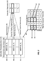
- Figure 1 is a block diagram of an exemplary processor-based system 10 for issuing instructions to execution pipelines 12(0-Q) (referred to herein as P 0 -P Q , respectively) based on register-associated preferences.
- the processor-based system 10 provides an instruction processing circuit 14 that is configured to determine execution pipeline preferences for the instructions.
- the instruction processing circuit may include an instruction detection circuit 15, a source register detection circuit 16, and a target register detection circuit 17.
- the instructions processed by the instruction processing circuit 14 may indicate operations for reading data from and/or writing data to registers 18(0-X) (referred to herein as R 0 -R X , respectively), which provide local high-speed storage accessible by the processor-based system 10.
- instructions may refer to a combination of bits defined by an instruction set architecture that directs a computer processor to carry out a specified task or tasks.
- instruction set architectures include, but are not limited to, ARM, Thumb, and A64 architectures.
- the instructions are processed in the processor-based system 10 in a continuous flow represented by an instruction stream 19.
- the instruction stream 19 may continuously advance while the processor-based system 10 is operating and executing the instructions.
- the instruction stream 19 begins with an instruction memory 20, which provides persistent storage for the instructions in a computer-executable program.
- An instruction fetch circuit 22 reads an instruction from the instruction memory 20 and/or optionally from an instruction cache 24, and may increment a program counter, which may be stored in one of the registers 18(0-X).
- the instruction decode circuit 26 translates the instruction into processor-specific microinstructions.
- the instruction decode circuit 26 holds a group of multiple instructions 28(0-N) simultaneously for decoding.
- the instructions are optionally issued to an instruction queue 30 (i.e., a buffer for storing instructions), or they may be issued to one of the execution pipelines 12(0-Q) for execution.
- instruction queue 30 i.e., a buffer for storing instructions
- particular execution pipelines 12(0-Q) may restrict the types of operations that may be carried out within that particular execution pipeline. For example, pipeline P 0 may not permit read access to the registers 18(0-X); accordingly, an instruction that indicates an operation to read register R 0 may only be issued to one of the execution pipelines P 1 through P Q .
- the instruction processing circuit 14 is configured to determine at least one execution pipeline preference for an instruction based on at least one pipeline indicator for at least one source register, and if at least one target register is specified, to update a pipeline indicator for the at least one target register based on the one of the execution pipelines 12(0-Q) to which the instruction is issued.
- the instruction processing circuit 14 may be any type of device or circuit, and may be implemented or performed with a processor, a Digital Signal Processor (DSP), an Application Specific Integrated Circuit (ASIC), a Field-Programmable Gate Array (FPGA) or other programmable logic device, discrete gate or transistor logic, discrete hardware components, or any combination thereof designed to perform the functions described herein.
- DSP Digital Signal Processor
- ASIC Application Specific Integrated Circuit
- FPGA Field-Programmable Gate Array
- the instruction processing circuit 14 is incorporated into the instruction fetch circuit 22, the instruction decode circuit 26, and/or the optional instruction queue 30.
- the instruction processing circuit 14 may also employ a pipeline issuance table 32 configured to store one or more pipeline indicators, which associate each of the registers 18(0-X) with one of the execution pipelines 12(0-Q) in which each of the registers 18(0-X) was most recently written.
- the pipeline issuance table 32 comprises a plurality of rows, with each row corresponding to one of the registers 18(0-X) and including at least one pipeline indicator.
- the at least one pipeline indicator is a Boolean flag corresponding to a respective one of the execution pipelines 12(0-Q); in some embodiments, the at least one pipeline indicator is a data value storing an identification of one of the execution pipelines 12(0-Q).
- Figure 2 depicts the instruction processing circuit 14 of Figure 1 processing a detected instruction stream 34.
- the processing includes issuing an instruction to one of the execution pipelines 12(0-Q) based on register-associated preferences.
- the detected instruction stream 34 represents a series of instructions fetched from the instruction stream 19 and detected by the instruction processing circuit 14 of Figure 1.
- An instruction 36 (in this example, a WRITE instruction) is fetched first from the detected instruction stream 34.
- the instruction 36 indicates an operation to write the contents of one of the registers 18(0-X) of Figure 1 (in this example, a source register R 2 ) into a target register R 1 , also one of the registers 18(0-X).
- the instruction 36 is issued to one of the execution pipelines 12(0-Q), referred to in this example as pipeline P 1 .
- a pipeline indicator 40 corresponding to the target register R 1 and the execution pipeline P 1 , is updated in the pipeline issuance table 32 by the instruction processing circuit 14 (as indicated by arrow 42).
- the pipeline issuance table 32 is used to track the one of the execution pipelines 12(0-Q) to which the most recent instruction to target a given one of the registers 18(0-X) for writing was issued.
- the pipeline issuance table 32 contains a row corresponding to each of the registers 18(0-X), with each row containing a plurality of pipeline indicators (e.g., the pipeline indicator 40) each corresponding to one of the execution pipelines 12(0-Q).
- Each pipeline indicator in the pipeline issuance table 32 is thus associated with exactly one of the registers 18(0-X) and one of the execution pipelines 12(0-Q).
- only one pipeline indicator may be set for a given one of the registers 18(0-X) at any given time.
- two or more of the registers 18(0-X) may each have a pipeline indicator set for the same one of the execution pipelines 12(0-Q).
- the pipeline indicator 40 is updated by clearing all pipeline indicators in a row 44 associated with the target register R 1 , and setting the pipeline indicator 40 to indicate that the instruction 36, which is the most recent instruction to target register R 1 for writing, was issued to the execution pipeline P 1 .
- the instruction processing circuit 14 next detects an instruction 46 (in this example, another WRITE instruction) in the detected instruction stream 34.
- the instruction 46 specifies the register R 1 as a source register, and indicates an operation to write the contents of the source register R 1 into a target register R 0 (one of the registers 18(0-X)). It is to be understood that the instruction 46 may be fetched immediately following the instruction 36 in the detected instruction stream 34, or the instruction 36 and the instruction 46 may be separated in the detected instruction stream 34 by other intervening instructions.
- the pipeline issuance table 32 is accessed by the instruction processing circuit 14 (as indicated by arrow 42) to determine whether a pipeline indicator is set in the row 44 for the source register R 1 .
- the pipeline indicator 40 in the pipeline issuance table 32 is set, indicating that the most recent instruction to target the source register R 1 for writing (here, the instruction 36) was issued to the execution pipeline P 1 .
- the instruction processing circuit 14 determines an execution pipeline preference 48, which indicates that the instruction 46 should be preferentially issued to the execution pipeline P 1 .
- the instruction 46 may be associated with a plurality of execution pipeline preferences 48, based on a plurality of pipeline indicators corresponding to a plurality of source registers for the instruction 46. It is to be further understood that, in some embodiments, there may be no guarantee that the instruction 46 will actually be issued to the execution pipeline P 1 , as indicated by the execution pipeline preference 48. Rather, the execution pipeline preference 48 may be considered as one of a number of factors in determining to which one of the execution pipelines 12(0-Q) the instruction 46 will be issued.
- the exemplary process described above with respect to the instruction 36 may be repeated for the instruction 46.
- the instruction 46 is issued to the preferred execution pipeline P 1 , as indicated by pipeline issuance arrow 50.
- a pipeline indicator 52 corresponding to the target register R 0 and the execution pipeline P 1 , is updated in the pipeline issuance table 32.
- the instruction processing circuit 14 may access the pipeline issuance table 32 to determine whether a pipeline indicator is set in a row 56 for the source register R 0 . Based on the pipeline indicator 52, the instruction processing circuit 14 determines an execution pipeline preference 58 indicating a preference for the execution pipeline P 1 for issuance of the instruction 54.
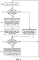
- FIG. 3 an exemplary generalized process for an instruction processing circuit configured to determine execution pipeline preferences and update pipeline indicators is shown in Figure 3 , with further reference to Figures 1 and 2 .
- the process begins as the instruction processing circuit 14 of Figure 1 (not shown) detects the instruction 46 of Figure 2 , indicating a write operation to the target register R 0 (block 60).
- detecting the instruction 46 may be accomplished by an instruction detection circuit such as the instruction detection circuit 15 of Figure 1.
- the instruction processing circuit 14 next determines whether the instruction 46 specifies at least one source register (block 62). Some embodiments may provide that this determination is made by a source register detection circuit of the instruction processing circuit 14, such as the source register detection circuit 16 of Figure 1. If the instruction 46 does not specify at least one source register, the instruction 46 is issued to an execution pipeline (e.g., one of the execution pipelines P 0 -P Q ) based on default execution pipeline issuance logic (block 64). If the instruction 46 does specify at least one source register, as in Figure 2 , the instruction processing circuit 14 determines at least one execution pipeline preference 48 based on the pipeline indicator(s) for the at least one source register in a pipeline issuance table 32 (block 66).
- an execution pipeline e.g., one of the execution pipelines P 0 -P Q
- default execution pipeline issuance logic block 64
- the instruction processing circuit 14 determines at least one execution pipeline preference 48 based on the pipeline indicator(s) for the at least one source register in a pipeline issuance table 32 (block 66).
- the execution pipeline preference 48 is based on the pipeline indicator 40 for the source register R 1 in the pipeline issuance table 32.
- the instruction 46 is then issued to an execution pipeline (in Figure 2 , the execution pipeline P 1 ) based on the at least one execution pipeline preference 48 (block 68).
- the instruction processing circuit 14 determines whether the instruction 46 specifies at least one target register (block 70). In some embodiments, this determination may be made by a target register detection circuit of the instruction processing circuit 14, such as the target register detection circuit 17 of Figure 1. If the instruction 46 does not specify at least one target register, processing returns to at block 60 of Figure 3 . If the instruction 46 does specify at least one target register, the instruction processing circuit 14 updates at least one pipeline indicator for the at least one target register in the pipeline issuance table 32 based on the execution pipeline to which the instruction 46 is issued (block 72). In Figure 2 , the pipeline indicator 52 for the target register R 0 is updated in the pipeline issuance table 32 based on the instruction 46 being issued to the execution pipeline P 1 . Processing then resumes at block 60 of Figure 3 .
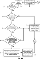
- Figures 4A-4B illustrate a more detailed exemplary process of an instruction processing circuit (e.g., the instruction processing circuit 14 in the processor-based system 10 of Figure 1) for detecting instructions in an instruction stream (e.g., the instruction stream 19 of Figure 1), and issuing the instructions to execution pipelines (such as the execution pipelines 12(0-Q) of Figure 1) based on register-associated preferences.
- Figure 4A details a process for determining whether a detected instruction specifies at least one source register, and determining at least one execution pipeline preference for the instruction.
- Figure 4B illustrates operations for updating a pipeline indicator (such as the pipeline indicators 40, 52 of Figure 2 ) in a pipeline issuance table (for instance, the pipeline issuance table 32 of Figure 1).
- the process in this example begins in Figure 4A with the instruction processing circuit detecting whether more instructions remain to be processed (block 74 of Figure 4A ). In some embodiments, this detection is accomplished by detecting a presence of unprocessed instructions in an instruction fetch circuit and/or an instruction decode circuit (such as the instruction fetch circuit 22 and/or the instruction decode circuit 26, respectively, of Figure 1). If no remaining instructions are detected, the instruction processing circuit performs validation of any pipeline indicators stored in a pipeline issuance table (e.g., the pipeline issuance table 32 of Figure 1). Validation may include verifying that a stored pipeline indicator remains valid for determining an execution pipeline preference for a corresponding register, and updating the pipeline issuance table accordingly (for example, by updating a validity bit for the pipeline indicator). Processing then returns to block 74 of Figure 4A .
- a pipeline issuance table e.g., the pipeline issuance table 32 of Figure 1). Validation may include verifying that a stored pipeline indicator remains valid for determining an execution pipeline preference for a corresponding register, and updating the pipeline
- the instruction processing circuit determines whether the detected instruction is an instruction specifying at least one source register (such as one of the registers 18(0-X) of Figure 1) (block 76 of Figure 4A ). Detection of such an instruction indicates that the instruction processing circuit may be able to determine at least one execution pipeline preference for the instruction. In the event that the detected instruction is not an instruction specifying at least one source register, the detected instruction is issued to an execution pipeline based on default execution pipeline issuance logic (block 78 of Figure 4A ), and processing continues to block 88 of Figure 4B .
- the detected instruction is an instruction specifying at least one source register (such as one of the registers 18(0-X) of Figure 1) (block 76 of Figure 4A ). Detection of such an instruction indicates that the instruction processing circuit may be able to determine at least one execution pipeline preference for the instruction. In the event that the detected instruction is not an instruction specifying at least one source register, the detected instruction is issued to an execution pipeline based on default execution pipeline issuance logic (block 78 of Figure 4A ),
- the instruction processing circuit next determines whether the instruction is one for which an execution pipeline preference should be determined based on the specified source register(s) (block 80 of Figure 4A ). In some embodiments, only a subset of the instructions specifying at least one source register may be analyzed to determine an execution pipeline preference. If the instruction is not one for which an execution pipeline preference should be determined, the instruction is issued to an execution pipeline based on default execution pipeline issuance logic (block 78 of Figure 4A ), and processing continues to block 88 of Figure 4B .
- the pipeline issuance table is accessed by the instruction processing circuit to determine whether any pipeline indicators associated with the at least one source register are set (block 82 of Figure 4A ). If no pipeline indicator associated with the at least one source register is set, the instruction is issued to an execution pipeline based on default execution pipeline issuance logic (block 78 of Figure 4A ), and processing continues to block 88 of Figure 4B . If at least one pipeline indicator associated with the at least one source register is set, the instruction processing circuit determines at least one execution pipeline preference for the instruction based on the at least one pipeline indicator set in the pipeline issuance table (block 84 of Figure 4A ). Based on the at least one execution pipeline preference determined in block 84 of Figure 4A , the instruction is then issued to an execution pipeline (block 86 of Figure 4A ), and processing continues at block 88 of Figure 4B .
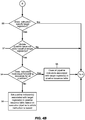
- the instruction processing circuit next determines whether the instruction specifies at least one target register (block 88 of Figure 4B ). If not, normal processing of the instruction continues at block 90 of Figure 4A . Otherwise, the instruction processing circuit determines whether the pipeline issuance table should be updated based on the target register of the instruction (block 92 of Figure 4B ). In some embodiments, the pipeline issuance table may be updated only for a subset of the instructions. If the instruction is not one for which the pipeline issuance table should be updated, normal processing of the instruction continues (block 90 of Figure 4A ).
- the instruction processing circuit next examines whether the instruction has equal forwarding resources for all pipelines (block 94 of Figure 4B ).
- the results of some instructions may be equally available for forwarding to subsequent instructions regardless of the execution pipelines to which the instructions and the subsequent instructions are issued. Thus, it may be said that such instructions have equal forwarding resources for all pipelines.
- the detected instruction has limited forwarding resources (i.e., if the detected instruction does not have equal forwarding resources for all pipelines)
- performance of the processor-based system may be improved by preferentially issuing subsequent instructions specifying the detected instruction's target register(s) as source register(s) to the same execution pipeline as the detected instruction.
- the instruction processing circuit sets pipeline indicator(s) associated with the at least one target register in the pipeline issuance table, based on the execution pipeline to which the detected instruction was issued (block 96 of Figure 4B ). Processing then resumes at block 90 of Figure 4A .
- the instruction processing circuit clears all pipeline indicators associated with the detected instruction's target register(s) in the pipeline issuance table to indicate that all pipelines have equal preference (block 98 of Figure 4B ). Processing then resumes at block 90 of Figure 4A .
- the pipeline issuance table 32 comprises a plurality of rows, with each row corresponding to one of the registers 18(0-X) and including at least one pipeline indicator.
- each pipeline indicator is a Boolean flag corresponding to one of the execution pipelines 12(0-Q).
- Figure 5 illustrates an exemplary sequence including issuing instructions to one of the execution pipelines 12(0-Q) based on register-associated preferences stored in a flag-based pipeline issuance table 100.
- the instruction processing circuit 14 of Figure 1 processes a detected instruction stream 102 representing a series of instructions fetched from the instruction stream 19 and detected by the instruction processing circuit 14 of Figure 1.
- the first detected instruction is an ARM architecture ADD instruction 104.
- the ADD instruction 104 indicates an operation to sum the contents of two of the registers 18(0-X) shown in Figure 1 (in this example, registers R 2 and R 3 ), and write the result into a target register R 1 , also one of the registers 18(0-X). As indicated by pipeline issuance arrow 106, the ADD instruction 104 is issued to one of the execution pipelines 12(0-Q), referred to in this example as pipeline P 1 .
- a pipeline indicator 108 corresponding to the target register R 1 and the execution pipeline P 1 , is updated in the flag-based pipeline issuance table 100 by the instruction processing circuit 14 (as indicated by arrow 110).
- Each pipeline indicator in the flag-based pipeline issuance table 100 is a Boolean flag associated with exactly one of the registers 18(0-X) and one of the execution pipelines 12(0-Q). In the example shown in Figure 5 , only one pipeline indicator may be set for a given one of the registers 18(0-X) at any given time, although two or more of the registers 18(0-X) may each have a pipeline indicator set for the same one of the execution pipelines 12(0-Q).
- the pipeline indicator 108 is updated by clearing all pipeline indicators in a row 112 associated with the target register R 1 , and setting the pipeline indicator 108 to indicate that the ADD instruction 104, which is the most recent instruction to target register R 1 for writing, was issued to the execution pipeline P 1 .
- the instruction processing circuit 14 next detects an ARM architecture MOV instruction 114 in the detected instruction stream 102.
- the MOV instruction 114 specifies the register R 1 as a source register, and indicates an operation to write the contents of the source register R 1 into a target register R 0 (one of registers 18(0-X)).
- the MOV instruction 114 may be fetched immediately following the ADD instruction 104 in the detected instruction stream 102, while according to some embodiments, the ADD instruction 104 and the MOV instruction 114 may be separated in the detected instruction stream 102 by other intervening instructions.
- the flag-based pipeline issuance table 100 is accessed by the instruction processing circuit 14 (as indicated by arrow 110) to determine whether a pipeline indicator is set in the row 112 for the source register R 1 .
- the pipeline indicator 108 in the flag-based pipeline issuance table 100 indicates that the most recent instruction to target the source register R 1 for writing (here, the ADD instruction 104) was issued to the execution pipeline P 1 .
- the instruction processing circuit 14 determines an execution pipeline preference 116 for pipeline P 1 , which indicates that the MOV instruction 114 should be preferentially issued to the execution pipeline P 1 .
- the MOV instruction 114 may be issued to the particular one of the execution pipelines 12(0-Q) indicated by the execution pipeline preference 116, as other factors may be taken into consideration in determining the most appropriate one of the execution pipelines 12(0-Q) to which an instruction issues.
- the MOV instruction 114 is issued to the execution pipeline P 2 , as indicated by pipeline issuance arrow 118, instead of to the preferred execution pipeline P 1 .
- a pipeline indicator 120 corresponding to the target register R 0 and the pipeline P 2 , is then updated in the flag-based pipeline issuance table 100.
- the instruction processing circuit 14 may access the flag-based pipeline issuance table 100 to determine whether a pipeline indicator is set in a row 124 for the source register R 0 . Based on the pipeline indicator 120, the instruction processing circuit 14 determines an execution pipeline preference 126, which indicates a preference for the pipeline P 2 for issuance of the MOV instruction 122. Issuance of the MOV instruction 122 and updating of the flag-based pipeline issuance table 100 based on the target register(s) of the MOV instruction 122 then proceeds as described above with respect to the ADD instruction 104 and the MOV instruction 114.
- each pipeline indicator stored in the pipeline issuance table 32 of Figure 1 includes a data value storing an identification of one of the execution pipelines 12(0-Q).
- Figure 6 illustrates an exemplary sequence including issuing instructions to one of the execution pipelines 12(0-Q) based on register-associated preferences stored in an identification-based pipeline issuance table 128.
- the instruction processing circuit 14 of Figure 1 processes a detected instruction stream 130 representing a series of instructions fetched from the instruction stream 19 and detected by the instruction processing circuit 14 of Figure 1.
- the first detected instruction is an ARM architecture MOV instruction 132.
- the MOV instruction 132 indicates an operation to copy the contents of one of the registers 18(0-X) shown in Figure 1 (in this example, source register R X ) into another one of the registers 18(0-X) (here, the target register R 0 ).
- the source register R X does not have a pipeline indicator set in the identification-based pipeline issuance table 128, and thus is not associated with any particular execution pipeline 12(0-Q).
- the MOV instruction 132 is issued to one of the execution pipelines 12(0-Q) (in this example, pipeline P 0 ) based on default execution pipeline issuance logic.
- the identification-based pipeline issuance table 128 is updated by the instruction processing circuit 14 (as indicated by arrow 136) to set a pipeline indicator 138, corresponding to the target register R 0 and the execution pipeline P 0 .
- Each pipeline indicator in the identification-based pipeline issuance table 128 is a data value associated with one of the registers 18(0-X) and identifying one of the execution pipelines 12(0-Q).
- the pipeline indicator 138 is updated by storing an identification of the execution pipeline P 0 to indicate that the MOV instruction 132, which is the most recent instruction to target register R 0 for writing, was issued to the execution pipeline P 0 .
- setting a pipeline indicator may also include setting a validity bit for each pipeline indicator to indicate whether or not the pipeline indicator is valid for use in determining an execution pipeline preference for the corresponding register. Accordingly, in this example, a validity bit 139 corresponding to the pipeline indicator 138 is set by the instruction processing circuit 14 to indicate that the pipeline indicator 138 is valid for use in determining an execution pipeline preference for target register R 0 .
- the instruction processing circuit 14 next detects a subsequent ARM architecture MOV instruction 140 in the detected instruction stream 130.
- the MOV instruction 140 indicates an operation to copy the source register R X into another one of the registers 18(0-X) (here, target register R 1 ).
- the MOV instruction 140 may be fetched immediately following the MOV instruction 132 in the detected instruction stream 130, while according to some embodiments, the MOV instruction 132 and the MOV instruction 140 may be separated in the detected instruction stream 130 by other intervening instructions.
- the source register R X does not have a pipeline indicator set in the identification-based pipeline issuance table 128; thus, as indicated by pipeline issuance arrow 142, the MOV instruction 140 is issued to one of the execution pipelines 12(0-Q) (here, pipeline P 1 ) based on default execution pipeline issuance logic.
- the identification-based pipeline issuance table 128 is then updated to set a pipeline indicator 144 corresponding to the target register R 1 and the execution pipeline P 1 .
- the pipeline indicator 144 stores an identification of the execution pipeline P 1 to indicate that the MOV instruction 140, which is the most recent instruction to target register R 1 for writing, was issued to the execution pipeline P 1 .
- a validity bit 145 corresponding to the pipeline indicator 144 is also set, to indicate that the pipeline indicator 144 is valid for use in determining an execution pipeline preference for target register R 1 .
- the instruction processing circuit 14 next detects an ARM architecture ADD instruction 146 in the detected instruction stream 130.
- the ADD instruction 146 indicates an operation to sum the contents of the source registers R 0 and R 1 , and store the result in the target register R 2 .
- the ADD instruction 146 may be fetched immediately following the MOV instruction 140 in the detected instruction stream 130, while according to some embodiments, the MOV instruction 140 and the ADD instruction 146 may be separated in the detected instruction stream 130 by other intervening instructions.
- the identification-based pipeline issuance table 128 is accessed by the instruction processing circuit 14 (as indicated by arrow 136) to determine whether a pipeline indicator is set in either or both of a row 148 corresponding to the source register R 0 , and a row 150 corresponding to the source register R 1 .
- the pipeline indicator 138 in the identification-based pipeline issuance table 128 indicates that the most recent instruction to target the source register R 0 for writing (here, the MOV instruction 132) was issued to the execution pipeline P 0 .
- the pipeline indicator 144 in the identification-based pipeline issuance table 128 indicates that the most recent instruction to target the source register R 1 for writing (in this example, the MOV instruction 140) was issued to the execution pipeline P 1 .
- the instruction processing circuit 14 determines two execution pipeline preferences 152, indicating that the ADD instruction 146 should be preferentially issued to either the execution pipeline P 0 or the execution pipeline P 1 .
- the ADD instruction 146 may be issued to either of the particular ones of the execution pipelines 12(0-Q) indicated by the execution pipeline preferences 152, as other factors may be taken into consideration in determining the most appropriate one of the execution pipelines 12(0-Q) for an instruction.
- some embodiments may apply additional execution pipeline issuance logic to select from among a plurality of preferred execution pipelines when more than one execution pipeline preferences are determined by the instruction processing circuit.
- the ADD instruction 146 is issued to the preferred execution pipeline P 1 , as indicated by pipeline issuance arrow 154.
- a pipeline indicator 156 and a validity bit 157, corresponding to the target register R 2 and the execution pipeline P 1 are then updated in the identification-based pipeline issuance table 128.
- the instruction processing circuits operable for issuing instructions to execution pipelines based on register-associated preferences may be provided in or integrated into any processor-based device. Examples, without limitation, include a set top box, an entertainment unit, a navigation device, a communications device, a fixed location data unit, a mobile location data unit, a mobile phone, a cellular phone, a computer, a portable computer, a desktop computer, a personal digital assistant (PDA), a monitor, a computer monitor, a television, a tuner, a radio, a satellite radio, a music player, a digital music player, a portable music player, a digital video player, a video player, a digital video disc (DVD) player, and a portable digital video player.
- PDA personal digital assistant
- FIG. 7 illustrates an example of a processor-based system 158 that can employ the instruction processing circuit 14 illustrated in Figure 1.
- the processor-based system 158 includes one or more central processing units (CPUs) 160, each including one or more processors 162.
- the processor(s) 162 may comprise the instruction processing circuit (IPC) 14.
- the CPU(s) 160 may have cache memory 164 coupled to the processor(s) 162 for rapid access to temporarily stored data.
- the CPU(s) 160 is coupled to a system bus 166 and can intercouple master and slave devices included in the processor-based system 158.
- the CPU(s) 160 communicates with these other devices by exchanging address, control, and data information over the system bus 166.
- the CPU(s) 160 can communicate bus transaction requests to a memory controller 168, as an example of a slave device.
- multiple system buses 166 could be provided.
- Other master and slave devices can be connected to the system bus 166. As illustrated in Figure 7 , these devices can include a memory system 170, one or more input devices 172, one or more output devices 174, one or more network interface devices 176, and one or more display controllers 178, as examples.
- the input device(s) 172 can include any type of input device, including but not limited to input keys, switches, voice processors, etc.
- the output device(s) 174 can include any type of output device, including but not limited to audio, video, other visual indicators, etc.
- the network interface device(s) 176 can be any device(s) configured to allow exchange of data to and from a network 180.
- the network 180 can be any type of network, including but not limited to a wired or wireless network, a private or public network, a local area network (LAN), a wide local area network (WLAN), and the Internet.
- the network interface device(s) 176 can be configured to support any type of communication protocol desired.
- the memory system 170 can include one or more memory units 182(0-N).
- the CPU(s) 160 may also be configured to access the display controller(s) 178 over the system bus 166 to control information sent to one or more displays 184.
- the display controller(s) 178 sends information to the display(s) 184 to be displayed via one or more video processors 186, which process the information to be displayed into a format suitable for the display(s) 184.
- the display(s) 184 can include any type of display, including but not limited to a cathode ray tube (CRT), a liquid crystal display (LCD), a plasma display, etc.
- a processor may be a microprocessor, but in the alternative, the processor may be any conventional processor, controller, microcontroller, or state machine.
- a processor may also be implemented as a combination of computing devices, e.g., a combination of a DSP and a microprocessor, a plurality of microprocessors, one or more microprocessors in conjunction with a DSP core, or any other such configuration.
- RAM Random Access Memory
- ROM Read Only Memory
- EPROM Electrically Programmable ROM
- EEPROM Electrically Erasable Programmable ROM
- registers hard disk, a removable disk, a CD-ROM, or any other form of computer readable medium known in the art.
- An exemplary storage medium is coupled to the processor such that the processor can read information from, and write information to, the storage medium.
- the storage medium may be integral to the processor.
- the processor and the storage medium may reside in an ASIC.
- the ASIC may reside in a remote station.
- the processor and the storage medium may reside as discrete components in a remote station, base station, or server.
Description
- The technology of the disclosure relates generally to processing of pipelined computer instructions in central processing unit (CPU)-based systems.
- The advent of "instruction pipelining" in modem computer architectures has yielded improved utilization of CPU resources and faster execution times of computer applications. Instruction pipelining is a processing technique whereby a throughput of instructions being processed by a CPU may be increased by splitting the processing of each instruction into a series of steps. The instructions are executed in an "execution pipeline" composed of multiple stages, with each stage carrying out one of the steps for each of a series of instructions. As a result, in each CPU clock cycle, steps for multiple instructions may be evaluated in parallel. A CPU may optionally employ multiple execution pipelines to further boost performance.
- Occasionally, circumstances may arise wherein an instruction is prevented from executing during its designated CPU clock cycle in an execution pipeline. For instance, a data dependency may exist between a first instruction and a subsequent instruction (i.e., the subsequent instruction may require data generated by an operation provided by the first instruction). If the first instruction has not completely executed before the subsequent instruction begins execution, the data required by the subsequent instruction may not yet be available when the subsequent instruction executes, and therefore a pipeline "hazard" (specifically, a "read after write hazard") will occur. To resolve this hazard, the CPU may "stall" or delay execution of the subsequent instruction until the first instruction has completely executed. To help avoid having to stall the subsequent instruction, the CPU may alternatively employ a technique known as "pipeline forwarding." Pipeline forwarding may prevent the need for stalling execution of the subsequent instruction by allowing a result of the first executed instruction to be accessed by the subsequent instruction without requiring the result to be written to a register and then read back from the register by the subsequent instruction.
-
US 6,728,866 discloses an example of a partitioned issue queue and allocation strategy. - Pipeline forwarding may take place between instructions executing within the same execution pipeline, a process which may be more specifically referred to as "intra-pipeline forwarding." In addition, pipeline forwarding may occur between instructions executing in separate execution pipelines, wherein the process is conventionally referred to as "inter-pipeline forwarding." A CPU may be configured to provide intra-pipeline forwarding within a single execution pipeline more efficiently and from more access points than inter-pipeline forwarding between two separate execution pipelines. While the performance of inter-pipeline forwarding may be improved by expanding the CPU's forwarding circuitry to effectively add more access points, a tradeoff may exist in the form of increased complexity of the CPU architecture.
- Embodiments of the disclosure, the features of which are set out in the appended claims, provide a method, processor, and computer readable medium for issuing instructions to execution pipelines based on register-associated preferences. Related instruction processing circuits, processor systems, methods, and computer-readable media are also disclosed. In this regard, in one embodiment, a method for processing computer instructions is provided. The method comprises detecting an instruction in an instruction stream. Upon determining that the instruction specifies at least one source register, at least one execution pipeline preference for the instruction is determined based on at least one pipeline indicator associated with the at least one source register in a pipeline issuance table, and the instruction is issued to an execution pipeline based on the at least one execution pipeline preference. The method additionally comprises, upon determining that the instruction specifies at least one target register, updating at least one pipeline indicator associated with the at least one target register in the pipeline issuance table based on the execution pipeline to which the instruction is issued. In this manner, optimal forwarding of instructions may be facilitated, thus improving processor performance.
- In another embodiment, a processor comprising an instruction processing circuit is provided. The instruction processing circuit comprises an instruction detection circuit configured to detect an instruction in an instruction stream, and a pipeline issuance table. The instruction processing circuit further comprises a source register detection circuit and a target register detection circuit. The source register detection circuit is configured to determine whether the instruction specifies at least one source register. In response to determining that the instruction specifies the at least one source register, the source register detection circuit is configured to determine at least one execution pipeline preference for the instruction based on at least one pipeline indicator associated with the at least one source register in the pipeline issuance table. The target register detection circuit is configured to determine whether the instruction specifies at least one target register. In response to determining that the instruction specifies the at least one target register, the target register detection circuit is configured to update at least one pipeline indicator associated with the at least one target register in the pipeline issuance table based on the execution pipeline to which the instruction is issued. The processor is configured to issue the instruction to an execution pipeline based on the at least one execution pipeline preference, responsive to the source register detection circuit determining that the instruction specifies the at least one source register.
- In another embodiment, a processor comprising an instruction processing circuit is provided. The instruction processing circuit comprises a means for detecting an instruction in an instruction stream. The instruction processing circuit further comprises a means for determining at least one execution pipeline preference for the instruction based on at least one pipeline indicator associated with at least one source register in a pipeline issuance table, responsive to determining that the instruction specifies the at least one source register. The instruction processing circuit also comprises a means for issuing the instruction to an execution pipeline based on the at least one execution pipeline preference, responsive to determining that the instruction specifies the at least one source register. The instruction processing circuit additionally comprises a means for updating at least one pipeline indicator associated with at least one target register in the pipeline issuance table based on the execution pipeline to which the instruction is issued, responsive to determining that the instruction specifies the at least one target register.
- In another embodiment, a non-transitory computer-readable medium is provided, having stored thereon computer-executable instructions to cause a processor to implement a method for detecting an instruction in an instruction stream. The method implemented by the computer-executable instructions also comprises, upon determining that the instruction specifies at least one source register, determining at least one execution pipeline preference for the instruction based on at least one pipeline indicator associated with the at least one source register in a pipeline issuance table, and issuing the instruction to an execution pipeline based on the at least one execution pipeline preference. The method implemented by the computer-executable instructions additionally comprises, upon determining that the instruction specifies at least one target register, updating at least one pipeline indicator associated with the at least one target register in the pipeline issuance table based on the execution pipeline to which the instruction is issued.
-
- Figure 1 is a block diagram of exemplary components provided in a processor-based system for retrieving and processing computer instructions to be placed into one or more execution pipelines, including an exemplary instruction processing circuit configured to issue instructions to the one or more execution pipelines based on register-associated preferences;
-
Figure 2 is a diagram illustrating an exemplary sequence in a processor-based system including issuing a first instruction to an execution pipeline, updating a pipeline indicator in a pipeline issuance table based on the execution pipeline, and preferentially issuing a subsequent instruction to the execution pipeline based on the pipeline indicator; -
Figure 3 is a flowchart illustrating an exemplary process of an instruction processing circuit for determining at least one execution pipeline preference for an instruction based on one or more source registers, issuing the instruction to an execution pipeline based on the at least one execution pipeline preference, and updating one or more pipeline indicators for one or more target registers based on the execution pipeline to which the instruction is issued; -
Figures 4A-4B are flowcharts illustrating a more detailed exemplary process of an instruction processing circuit for issuing instructions to execution pipelines based on register-associated preferences; -
Figure 5 is a diagram illustrating an exemplary sequence including issuing instructions to execution pipelines based on register-associated preferences stored in a flag-based pipeline issuance table; -
Figure 6 is a diagram illustrating an exemplary sequence including issuing instructions to execution pipelines based on register-associated preferences stored in an identification-based pipeline issuance table; and -
Figure 7 is a block diagram of an exemplary processor-based system that can include instruction processing circuits, including the instruction processing circuit of Figure 1, configured to issue instructions to execution pipelines based on register-associated preferences. - With reference now to the drawing figures, several exemplary embodiments of the present disclosure are described. The word "exemplary" is used herein to mean "serving as an example, instance, or illustration." Any embodiment described herein as "exemplary" is not necessarily to be construed as preferred or advantageous over other embodiments.
- Embodiments of the disclosure provide issuing instructions to execution pipelines based on register-associated preferences. Related instruction processing circuits, processor systems, methods, and computer-readable media are also disclosed. In this regard, in one embodiment, a method for processing computer instructions is provided. The method comprises detecting an instruction in an instruction stream. Upon determining that the instruction specifies at least one source register, at least one execution pipeline preference for the instruction is determined based on at least one pipeline indicator associated with the at least one source register in a pipeline issuance table, and the instruction is issued to an execution pipeline based on the at least one execution pipeline preference. The method additionally comprises, upon determining that the instruction specifies at least one target register, updating at least one pipeline indicator associated with the at least one target register in the pipeline issuance table based on the execution pipeline to which the instruction is issued. In this manner, optimal forwarding of instructions may be facilitated, thus improving processor performance.
- In this regard, Figure 1 is a block diagram of an exemplary processor-based system 10 for issuing instructions to execution pipelines 12(0-Q) (referred to herein as P0-PQ, respectively) based on register-associated preferences. As will be discussed in more detail below, the processor-based system 10 provides an
instruction processing circuit 14 that is configured to determine execution pipeline preferences for the instructions. In some embodiments, the instruction processing circuit may include an instruction detection circuit 15, a source register detection circuit 16, and a target register detection circuit 17. The instructions processed by theinstruction processing circuit 14 may indicate operations for reading data from and/or writing data to registers 18(0-X) (referred to herein as R0-RX, respectively), which provide local high-speed storage accessible by the processor-based system 10. As discussed herein, "instructions" may refer to a combination of bits defined by an instruction set architecture that directs a computer processor to carry out a specified task or tasks. Exemplary instruction set architectures include, but are not limited to, ARM, Thumb, and A64 architectures. - With continuing reference to Figure 1, the instructions are processed in the processor-based system 10 in a continuous flow represented by an instruction stream 19. The instruction stream 19 may continuously advance while the processor-based system 10 is operating and executing the instructions. In this illustrated example, the instruction stream 19 begins with an instruction memory 20, which provides persistent storage for the instructions in a computer-executable program. An instruction fetch circuit 22 reads an instruction from the instruction memory 20 and/or optionally from an instruction cache 24, and may increment a program counter, which may be stored in one of the registers 18(0-X).
- Once the instruction is fetched by the instruction fetch circuit 22, it proceeds to an instruction decode circuit 26, which translates the instruction into processor-specific microinstructions. In this embodiment, the instruction decode circuit 26 holds a group of multiple instructions 28(0-N) simultaneously for decoding. After the instructions have been fetched and decoded, they are optionally issued to an instruction queue 30 (i.e., a buffer for storing instructions), or they may be issued to one of the execution pipelines 12(0-Q) for execution. In some embodiments, particular execution pipelines 12(0-Q) may restrict the types of operations that may be carried out within that particular execution pipeline. For example, pipeline P0 may not permit read access to the registers 18(0-X); accordingly, an instruction that indicates an operation to read register R0 may only be issued to one of the execution pipelines P1 through PQ.
- With continuing reference to Figure 1, the
instruction processing circuit 14 is configured to determine at least one execution pipeline preference for an instruction based on at least one pipeline indicator for at least one source register, and if at least one target register is specified, to update a pipeline indicator for the at least one target register based on the one of the execution pipelines 12(0-Q) to which the instruction is issued. Theinstruction processing circuit 14 may be any type of device or circuit, and may be implemented or performed with a processor, a Digital Signal Processor (DSP), an Application Specific Integrated Circuit (ASIC), a Field-Programmable Gate Array (FPGA) or other programmable logic device, discrete gate or transistor logic, discrete hardware components, or any combination thereof designed to perform the functions described herein. In some embodiments, theinstruction processing circuit 14 is incorporated into the instruction fetch circuit 22, the instruction decode circuit 26, and/or the optional instruction queue 30. Theinstruction processing circuit 14 may also employ a pipeline issuance table 32 configured to store one or more pipeline indicators, which associate each of the registers 18(0-X) with one of the execution pipelines 12(0-Q) in which each of the registers 18(0-X) was most recently written. The pipeline issuance table 32 comprises a plurality of rows, with each row corresponding to one of the registers 18(0-X) and including at least one pipeline indicator. According to some embodiments described herein, the at least one pipeline indicator is a Boolean flag corresponding to a respective one of the execution pipelines 12(0-Q); in some embodiments, the at least one pipeline indicator is a data value storing an identification of one of the execution pipelines 12(0-Q). - To provide an illustration of an exemplary processing sequence in the processor-based system 10 of Figure 1,
Figure 2 is provided.Figure 2 depicts theinstruction processing circuit 14 of Figure 1 processing a detectedinstruction stream 34. The processing includes issuing an instruction to one of the execution pipelines 12(0-Q) based on register-associated preferences. The detectedinstruction stream 34 represents a series of instructions fetched from the instruction stream 19 and detected by theinstruction processing circuit 14 of Figure 1. - An instruction 36 (in this example, a WRITE instruction) is fetched first from the detected
instruction stream 34. Theinstruction 36 indicates an operation to write the contents of one of the registers 18(0-X) of Figure 1 (in this example, a source register R2) into a target register R1, also one of the registers 18(0-X). As indicated bypipeline issuance arrow 38, theinstruction 36 is issued to one of the execution pipelines 12(0-Q), referred to in this example as pipeline P1. - After the
instruction 36 is issued to the execution pipeline P1, apipeline indicator 40, corresponding to the target register R1 and the execution pipeline P1, is updated in the pipeline issuance table 32 by the instruction processing circuit 14 (as indicated by arrow 42). The pipeline issuance table 32 is used to track the one of the execution pipelines 12(0-Q) to which the most recent instruction to target a given one of the registers 18(0-X) for writing was issued. In this example, the pipeline issuance table 32 contains a row corresponding to each of the registers 18(0-X), with each row containing a plurality of pipeline indicators (e.g., the pipeline indicator 40) each corresponding to one of the execution pipelines 12(0-Q). Each pipeline indicator in the pipeline issuance table 32 is thus associated with exactly one of the registers 18(0-X) and one of the execution pipelines 12(0-Q). In the embodiment depicted inFigure 2 , only one pipeline indicator may be set for a given one of the registers 18(0-X) at any given time. However, two or more of the registers 18(0-X) may each have a pipeline indicator set for the same one of the execution pipelines 12(0-Q). Accordingly, in this example, thepipeline indicator 40 is updated by clearing all pipeline indicators in arow 44 associated with the target register R1, and setting thepipeline indicator 40 to indicate that theinstruction 36, which is the most recent instruction to target register R1 for writing, was issued to the execution pipeline P1. - The
instruction processing circuit 14 next detects an instruction 46 (in this example, another WRITE instruction) in the detectedinstruction stream 34. Theinstruction 46 specifies the register R1 as a source register, and indicates an operation to write the contents of the source register R1 into a target register R0 (one of the registers 18(0-X)). It is to be understood that theinstruction 46 may be fetched immediately following theinstruction 36 in the detectedinstruction stream 34, or theinstruction 36 and theinstruction 46 may be separated in the detectedinstruction stream 34 by other intervening instructions. - After the
instruction 46 is detected, the pipeline issuance table 32 is accessed by the instruction processing circuit 14 (as indicated by arrow 42) to determine whether a pipeline indicator is set in therow 44 for the source register R1. In this example, thepipeline indicator 40 in the pipeline issuance table 32 is set, indicating that the most recent instruction to target the source register R1 for writing (here, the instruction 36) was issued to the execution pipeline P1. Based on thepipeline indicator 40, theinstruction processing circuit 14 determines anexecution pipeline preference 48, which indicates that theinstruction 46 should be preferentially issued to the execution pipeline P1. It is to be understood that, in some embodiments, theinstruction 46 may be associated with a plurality ofexecution pipeline preferences 48, based on a plurality of pipeline indicators corresponding to a plurality of source registers for theinstruction 46. It is to be further understood that, in some embodiments, there may be no guarantee that theinstruction 46 will actually be issued to the execution pipeline P1, as indicated by theexecution pipeline preference 48. Rather, theexecution pipeline preference 48 may be considered as one of a number of factors in determining to which one of the execution pipelines 12(0-Q) theinstruction 46 will be issued. - Once the
instruction 46 issues to one of the execution pipelines 12(0-Q) (whether the execution pipeline P1 or another one of the execution pipelines 12(0-Q)), the exemplary process described above with respect to theinstruction 36 may be repeated for theinstruction 46. In this example, theinstruction 46 is issued to the preferred execution pipeline P1, as indicated bypipeline issuance arrow 50. Apipeline indicator 52, corresponding to the target register R0 and the execution pipeline P1, is updated in the pipeline issuance table 32. For a subsequent instruction 54 (in this example, another WRITE instruction) in the detectedinstruction stream 34 that specifies the register R0 as a source register, theinstruction processing circuit 14 may access the pipeline issuance table 32 to determine whether a pipeline indicator is set in arow 56 for the source register R0. Based on thepipeline indicator 52, theinstruction processing circuit 14 determines anexecution pipeline preference 58 indicating a preference for the execution pipeline P1 for issuance of theinstruction 54. - To further illustrate the process of issuing instructions to execution pipelines based on register-associated preferences, an exemplary generalized process for an instruction processing circuit configured to determine execution pipeline preferences and update pipeline indicators is shown in
Figure 3 , with further reference toFigures 1 and 2 . In this example, the process begins as theinstruction processing circuit 14 of Figure 1 (not shown) detects theinstruction 46 ofFigure 2 , indicating a write operation to the target register R0 (block 60). In some embodiments, detecting theinstruction 46 may be accomplished by an instruction detection circuit such as the instruction detection circuit 15 of Figure 1. - The
instruction processing circuit 14 next determines whether theinstruction 46 specifies at least one source register (block 62). Some embodiments may provide that this determination is made by a source register detection circuit of theinstruction processing circuit 14, such as the source register detection circuit 16 of Figure 1. If theinstruction 46 does not specify at least one source register, theinstruction 46 is issued to an execution pipeline (e.g., one of the execution pipelines P0-PQ) based on default execution pipeline issuance logic (block 64). If theinstruction 46 does specify at least one source register, as inFigure 2 , theinstruction processing circuit 14 determines at least oneexecution pipeline preference 48 based on the pipeline indicator(s) for the at least one source register in a pipeline issuance table 32 (block 66). In the example illustrated inFigure 2 , theexecution pipeline preference 48 is based on thepipeline indicator 40 for the source register R1 in the pipeline issuance table 32. Theinstruction 46 is then issued to an execution pipeline (inFigure 2 , the execution pipeline P1) based on the at least one execution pipeline preference 48 (block 68). - Once the
instruction 46 is issued to the execution pipeline, whether based on the default execution pipeline issuance logic as inblock 64 or the at least oneexecution pipeline preference 48 as inblock 68, theinstruction processing circuit 14 determines whether theinstruction 46 specifies at least one target register (block 70). In some embodiments, this determination may be made by a target register detection circuit of theinstruction processing circuit 14, such as the target register detection circuit 17 of Figure 1. If theinstruction 46 does not specify at least one target register, processing returns to atblock 60 ofFigure 3 . If theinstruction 46 does specify at least one target register, theinstruction processing circuit 14 updates at least one pipeline indicator for the at least one target register in the pipeline issuance table 32 based on the execution pipeline to which theinstruction 46 is issued (block 72). InFigure 2 , thepipeline indicator 52 for the target register R0 is updated in the pipeline issuance table 32 based on theinstruction 46 being issued to the execution pipeline P1. Processing then resumes atblock 60 ofFigure 3 . -
Figures 4A-4B illustrate a more detailed exemplary process of an instruction processing circuit (e.g., theinstruction processing circuit 14 in the processor-based system 10 of Figure 1) for detecting instructions in an instruction stream (e.g., the instruction stream 19 of Figure 1), and issuing the instructions to execution pipelines (such as the execution pipelines 12(0-Q) of Figure 1) based on register-associated preferences.Figure 4A details a process for determining whether a detected instruction specifies at least one source register, and determining at least one execution pipeline preference for the instruction.Figure 4B illustrates operations for updating a pipeline indicator (such as thepipeline indicators Figure 2 ) in a pipeline issuance table (for instance, the pipeline issuance table 32 of Figure 1). - The process in this example begins in
Figure 4A with the instruction processing circuit detecting whether more instructions remain to be processed (block 74 ofFigure 4A ). In some embodiments, this detection is accomplished by detecting a presence of unprocessed instructions in an instruction fetch circuit and/or an instruction decode circuit (such as the instruction fetch circuit 22 and/or the instruction decode circuit 26, respectively, of Figure 1). If no remaining instructions are detected, the instruction processing circuit performs validation of any pipeline indicators stored in a pipeline issuance table (e.g., the pipeline issuance table 32 of Figure 1). Validation may include verifying that a stored pipeline indicator remains valid for determining an execution pipeline preference for a corresponding register, and updating the pipeline issuance table accordingly (for example, by updating a validity bit for the pipeline indicator). Processing then returns to block 74 ofFigure 4A . - If a remaining instruction is detected, the instruction processing circuit determines whether the detected instruction is an instruction specifying at least one source register (such as one of the registers 18(0-X) of Figure 1) (block 76 of
Figure 4A ). Detection of such an instruction indicates that the instruction processing circuit may be able to determine at least one execution pipeline preference for the instruction. In the event that the detected instruction is not an instruction specifying at least one source register, the detected instruction is issued to an execution pipeline based on default execution pipeline issuance logic (block 78 ofFigure 4A ), and processing continues to block 88 ofFigure 4B . - Returning to the decision point at
block 76 ofFigure 4A , if the detected instruction is an instruction specifying at least one source register, the instruction processing circuit next determines whether the instruction is one for which an execution pipeline preference should be determined based on the specified source register(s) (block 80 ofFigure 4A ). In some embodiments, only a subset of the instructions specifying at least one source register may be analyzed to determine an execution pipeline preference. If the instruction is not one for which an execution pipeline preference should be determined, the instruction is issued to an execution pipeline based on default execution pipeline issuance logic (block 78 ofFigure 4A ), and processing continues to block 88 ofFigure 4B . - If an execution pipeline preference is to be determined for the instruction, the pipeline issuance table is accessed by the instruction processing circuit to determine whether any pipeline indicators associated with the at least one source register are set (block 82 of
Figure 4A ). If no pipeline indicator associated with the at least one source register is set, the instruction is issued to an execution pipeline based on default execution pipeline issuance logic (block 78 ofFigure 4A ), and processing continues to block 88 ofFigure 4B . If at least one pipeline indicator associated with the at least one source register is set, the instruction processing circuit determines at least one execution pipeline preference for the instruction based on the at least one pipeline indicator set in the pipeline issuance table (block 84 ofFigure 4A ). Based on the at least one execution pipeline preference determined inblock 84 ofFigure 4A , the instruction is then issued to an execution pipeline (block 86 ofFigure 4A ), and processing continues atblock 88 ofFigure 4B . - Referring now to
Figure 4B , the instruction processing circuit next determines whether the instruction specifies at least one target register (block 88 ofFigure 4B ). If not, normal processing of the instruction continues atblock 90 ofFigure 4A . Otherwise, the instruction processing circuit determines whether the pipeline issuance table should be updated based on the target register of the instruction (block 92 ofFigure 4B ). In some embodiments, the pipeline issuance table may be updated only for a subset of the instructions. If the instruction is not one for which the pipeline issuance table should be updated, normal processing of the instruction continues (block 90 ofFigure 4A ). - If the instruction is one for which the pipeline issuance table should be updated, the instruction processing circuit next examines whether the instruction has equal forwarding resources for all pipelines (block 94 of
Figure 4B ). In some embodiments, the results of some instructions may be equally available for forwarding to subsequent instructions regardless of the execution pipelines to which the instructions and the subsequent instructions are issued. Thus, it may be said that such instructions have equal forwarding resources for all pipelines. If the detected instruction has limited forwarding resources (i.e., if the detected instruction does not have equal forwarding resources for all pipelines), then performance of the processor-based system may be improved by preferentially issuing subsequent instructions specifying the detected instruction's target register(s) as source register(s) to the same execution pipeline as the detected instruction. Accordingly, the instruction processing circuit sets pipeline indicator(s) associated with the at least one target register in the pipeline issuance table, based on the execution pipeline to which the detected instruction was issued (block 96 ofFigure 4B ). Processing then resumes atblock 90 ofFigure 4A . - Returning now to the decision point at
block 94 ofFigure 4B , if the instruction does have equal forwarding resources for all pipelines, preferentially issuing subsequent instructions to the same execution pipeline as the detected instruction will not result in a performance advantage, and, in fact, flexibility in issuing instructions to execution pipelines may be constrained. Thus, in that scenario, the instruction processing circuit clears all pipeline indicators associated with the detected instruction's target register(s) in the pipeline issuance table to indicate that all pipelines have equal preference (block 98 ofFigure 4B ). Processing then resumes atblock 90 ofFigure 4A . - As noted above with respect to Figure 1, the pipeline issuance table 32 comprises a plurality of rows, with each row corresponding to one of the registers 18(0-X) and including at least one pipeline indicator. In some embodiments described herein, each pipeline indicator is a Boolean flag corresponding to one of the execution pipelines 12(0-Q). In this regard,
Figure 5 illustrates an exemplary sequence including issuing instructions to one of the execution pipelines 12(0-Q) based on register-associated preferences stored in a flag-based pipeline issuance table 100. InFigure 5 , theinstruction processing circuit 14 of Figure 1 processes a detected instruction stream 102 representing a series of instructions fetched from the instruction stream 19 and detected by theinstruction processing circuit 14 of Figure 1. The first detected instruction is an ARMarchitecture ADD instruction 104. TheADD instruction 104 indicates an operation to sum the contents of two of the registers 18(0-X) shown in Figure 1 (in this example, registers R2 and R3), and write the result into a target register R1, also one of the registers 18(0-X). As indicated bypipeline issuance arrow 106, theADD instruction 104 is issued to one of the execution pipelines 12(0-Q), referred to in this example as pipeline P1. - After the
ADD instruction 104 is issued to the execution pipeline P1, apipeline indicator 108, corresponding to the target register R1 and the execution pipeline P1, is updated in the flag-based pipeline issuance table 100 by the instruction processing circuit 14 (as indicated by arrow 110). Each pipeline indicator in the flag-based pipeline issuance table 100 is a Boolean flag associated with exactly one of the registers 18(0-X) and one of the execution pipelines 12(0-Q). In the example shown inFigure 5 , only one pipeline indicator may be set for a given one of the registers 18(0-X) at any given time, although two or more of the registers 18(0-X) may each have a pipeline indicator set for the same one of the execution pipelines 12(0-Q). Accordingly, thepipeline indicator 108 is updated by clearing all pipeline indicators in arow 112 associated with the target register R1, and setting thepipeline indicator 108 to indicate that theADD instruction 104, which is the most recent instruction to target register R1 for writing, was issued to the execution pipeline P1. - The
instruction processing circuit 14 next detects an ARMarchitecture MOV instruction 114 in the detected instruction stream 102. TheMOV instruction 114 specifies the register R1 as a source register, and indicates an operation to write the contents of the source register R1 into a target register R0 (one of registers 18(0-X)). In some embodiments, theMOV instruction 114 may be fetched immediately following theADD instruction 104 in the detected instruction stream 102, while according to some embodiments, theADD instruction 104 and theMOV instruction 114 may be separated in the detected instruction stream 102 by other intervening instructions. - After the
MOV instruction 114 is detected, the flag-based pipeline issuance table 100 is accessed by the instruction processing circuit 14 (as indicated by arrow 110) to determine whether a pipeline indicator is set in therow 112 for the source register R1. In this example, thepipeline indicator 108 in the flag-based pipeline issuance table 100 indicates that the most recent instruction to target the source register R1 for writing (here, the ADD instruction 104) was issued to the execution pipeline P1. Based on thepipeline indicator 108, theinstruction processing circuit 14 determines anexecution pipeline preference 116 for pipeline P1, which indicates that theMOV instruction 114 should be preferentially issued to the execution pipeline P1. - As noted above, in some embodiments there may be no guarantee that the
MOV instruction 114 will actually be issued to the particular one of the execution pipelines 12(0-Q) indicated by theexecution pipeline preference 116, as other factors may be taken into consideration in determining the most appropriate one of the execution pipelines 12(0-Q) to which an instruction issues. In this example, theMOV instruction 114 is issued to the execution pipeline P2, as indicated bypipeline issuance arrow 118, instead of to the preferred execution pipeline P1. Once theMOV instruction 114 issues to the execution pipeline P2, apipeline indicator 120, corresponding to the target register R0 and the pipeline P2, is then updated in the flag-based pipeline issuance table 100. - For a
subsequent MOV instruction 122 in the detected instruction stream 102 that specifies the register R0 as a source register, theinstruction processing circuit 14 may access the flag-based pipeline issuance table 100 to determine whether a pipeline indicator is set in arow 124 for the source register R0. Based on thepipeline indicator 120, theinstruction processing circuit 14 determines anexecution pipeline preference 126, which indicates a preference for the pipeline P2 for issuance of theMOV instruction 122. Issuance of theMOV instruction 122 and updating of the flag-based pipeline issuance table 100 based on the target register(s) of theMOV instruction 122 then proceeds as described above with respect to theADD instruction 104 and theMOV instruction 114. - Some embodiments may provide that each pipeline indicator stored in the pipeline issuance table 32 of Figure 1 includes a data value storing an identification of one of the execution pipelines 12(0-Q). In this regard,
Figure 6 illustrates an exemplary sequence including issuing instructions to one of the execution pipelines 12(0-Q) based on register-associated preferences stored in an identification-based pipeline issuance table 128. InFigure 6 , theinstruction processing circuit 14 of Figure 1 processes a detectedinstruction stream 130 representing a series of instructions fetched from the instruction stream 19 and detected by theinstruction processing circuit 14 of Figure 1. The first detected instruction is an ARMarchitecture MOV instruction 132. TheMOV instruction 132 indicates an operation to copy the contents of one of the registers 18(0-X) shown in Figure 1 (in this example, source register RX) into another one of the registers 18(0-X) (here, the target register R0). In this example, the source register RX does not have a pipeline indicator set in the identification-based pipeline issuance table 128, and thus is not associated with any particular execution pipeline 12(0-Q). Accordingly, as indicated bypipeline issuance arrow 134, theMOV instruction 132 is issued to one of the execution pipelines 12(0-Q) (in this example, pipeline P0) based on default execution pipeline issuance logic. - After the
MOV instruction 132 is issued to the execution pipeline P0, the identification-based pipeline issuance table 128 is updated by the instruction processing circuit 14 (as indicated by arrow 136) to set apipeline indicator 138, corresponding to the target register R0 and the execution pipeline P0. Each pipeline indicator in the identification-based pipeline issuance table 128 is a data value associated with one of the registers 18(0-X) and identifying one of the execution pipelines 12(0-Q). In this example, thepipeline indicator 138 is updated by storing an identification of the execution pipeline P0 to indicate that theMOV instruction 132, which is the most recent instruction to target register R0 for writing, was issued to the execution pipeline P0. In some embodiments, setting a pipeline indicator may also include setting a validity bit for each pipeline indicator to indicate whether or not the pipeline indicator is valid for use in determining an execution pipeline preference for the corresponding register. Accordingly, in this example, avalidity bit 139 corresponding to thepipeline indicator 138 is set by theinstruction processing circuit 14 to indicate that thepipeline indicator 138 is valid for use in determining an execution pipeline preference for target register R0. - The
instruction processing circuit 14 next detects a subsequent ARMarchitecture MOV instruction 140 in the detectedinstruction stream 130. TheMOV instruction 140 indicates an operation to copy the source register RX into another one of the registers 18(0-X) (here, target register R1). In some embodiments, theMOV instruction 140 may be fetched immediately following theMOV instruction 132 in the detectedinstruction stream 130, while according to some embodiments, theMOV instruction 132 and theMOV instruction 140 may be separated in the detectedinstruction stream 130 by other intervening instructions. As before, the source register RX does not have a pipeline indicator set in the identification-based pipeline issuance table 128; thus, as indicated bypipeline issuance arrow 142, theMOV instruction 140 is issued to one of the execution pipelines 12(0-Q) (here, pipeline P1) based on default execution pipeline issuance logic. The identification-based pipeline issuance table 128 is then updated to set apipeline indicator 144 corresponding to the target register R1 and the execution pipeline P1. In this regard, thepipeline indicator 144 stores an identification of the execution pipeline P1 to indicate that theMOV instruction 140, which is the most recent instruction to target register R1 for writing, was issued to the execution pipeline P1.A validity bit 145 corresponding to thepipeline indicator 144 is also set, to indicate that thepipeline indicator 144 is valid for use in determining an execution pipeline preference for target register R1. - The
instruction processing circuit 14 next detects an ARMarchitecture ADD instruction 146 in the detectedinstruction stream 130. TheADD instruction 146 indicates an operation to sum the contents of the source registers R0 and R1, and store the result in the target register R2. In some embodiments, theADD instruction 146 may be fetched immediately following theMOV instruction 140 in the detectedinstruction stream 130, while according to some embodiments, theMOV instruction 140 and theADD instruction 146 may be separated in the detectedinstruction stream 130 by other intervening instructions. - After the
ADD instruction 146 is detected, the identification-based pipeline issuance table 128 is accessed by the instruction processing circuit 14 (as indicated by arrow 136) to determine whether a pipeline indicator is set in either or both of arow 148 corresponding to the source register R0, and arow 150 corresponding to the source register R1. In this example, thepipeline indicator 138 in the identification-based pipeline issuance table 128 indicates that the most recent instruction to target the source register R0 for writing (here, the MOV instruction 132) was issued to the execution pipeline P0. Additionally, thepipeline indicator 144 in the identification-based pipeline issuance table 128 indicates that the most recent instruction to target the source register R1 for writing (in this example, the MOV instruction 140) was issued to the execution pipeline P1. Based on thepipeline indicator 138 and thepipeline indicator 144, theinstruction processing circuit 14 determines twoexecution pipeline preferences 152, indicating that theADD instruction 146 should be preferentially issued to either the execution pipeline P0 or the execution pipeline P1. - As noted above, in some embodiments, there may be no guarantee that the
ADD instruction 146 will be issued to either of the particular ones of the execution pipelines 12(0-Q) indicated by theexecution pipeline preferences 152, as other factors may be taken into consideration in determining the most appropriate one of the execution pipelines 12(0-Q) for an instruction. Likewise, some embodiments may apply additional execution pipeline issuance logic to select from among a plurality of preferred execution pipelines when more than one execution pipeline preferences are determined by the instruction processing circuit. In this example, theADD instruction 146 is issued to the preferred execution pipeline P1, as indicated bypipeline issuance arrow 154. Apipeline indicator 156 and avalidity bit 157, corresponding to the target register R2 and the execution pipeline P1, are then updated in the identification-based pipeline issuance table 128. - The instruction processing circuits operable for issuing instructions to execution pipelines based on register-associated preferences, according to embodiments disclosed herein, may be provided in or integrated into any processor-based device. Examples, without limitation, include a set top box, an entertainment unit, a navigation device, a communications device, a fixed location data unit, a mobile location data unit, a mobile phone, a cellular phone, a computer, a portable computer, a desktop computer, a personal digital assistant (PDA), a monitor, a computer monitor, a television, a tuner, a radio, a satellite radio, a music player, a digital music player, a portable music player, a digital video player, a video player, a digital video disc (DVD) player, and a portable digital video player.
- In this regard,
Figure 7 illustrates an example of a processor-basedsystem 158 that can employ theinstruction processing circuit 14 illustrated in Figure 1. In this example, the processor-basedsystem 158 includes one or more central processing units (CPUs) 160, each including one ormore processors 162. The processor(s) 162 may comprise the instruction processing circuit (IPC) 14. The CPU(s) 160 may havecache memory 164 coupled to the processor(s) 162 for rapid access to temporarily stored data. The CPU(s) 160 is coupled to a system bus 166 and can intercouple master and slave devices included in the processor-basedsystem 158. As is well known, the CPU(s) 160 communicates with these other devices by exchanging address, control, and data information over the system bus 166. For example, the CPU(s) 160 can communicate bus transaction requests to amemory controller 168, as an example of a slave device. Although not illustrated inFigure 7 , multiple system buses 166 could be provided. - Other master and slave devices can be connected to the system bus 166. As illustrated in
Figure 7 , these devices can include amemory system 170, one ormore input devices 172, one ormore output devices 174, one or morenetwork interface devices 176, and one ormore display controllers 178, as examples. The input device(s) 172 can include any type of input device, including but not limited to input keys, switches, voice processors, etc. The output device(s) 174 can include any type of output device, including but not limited to audio, video, other visual indicators, etc. The network interface device(s) 176 can be any device(s) configured to allow exchange of data to and from anetwork 180. Thenetwork 180 can be any type of network, including but not limited to a wired or wireless network, a private or public network, a local area network (LAN), a wide local area network (WLAN), and the Internet. The network interface device(s) 176 can be configured to support any type of communication protocol desired. Thememory system 170 can include one or more memory units 182(0-N). - The CPU(s) 160 may also be configured to access the display controller(s) 178 over the system bus 166 to control information sent to one or
more displays 184. The display controller(s) 178 sends information to the display(s) 184 to be displayed via one ormore video processors 186, which process the information to be displayed into a format suitable for the display(s) 184. The display(s) 184 can include any type of display, including but not limited to a cathode ray tube (CRT), a liquid crystal display (LCD), a plasma display, etc. - Those of skill in the art will further appreciate that the various illustrative logical blocks, modules, circuits, and algorithms described in connection with the embodiments disclosed herein may be implemented as electronic hardware, instructions stored in memory or in another computer-readable medium and executed by a processor or other processing device, or combinations of both. The master devices and slave devices described herein may be employed in any circuit, hardware component, integrated circuit (IC), IC chip, or semiconductor die, as examples. Memory disclosed herein may be any type and size of memory and may be configured to store any type of information desired. To clearly illustrate this interchangeability, various illustrative components, blocks, modules, circuits, and steps have been described above generally in terms of their functionality. How such functionality is implemented depends upon the particular application, design choices, and/or design constraints imposed on the overall system. Skilled artisans may implement the described functionality in varying ways for each particular application, but such implementation decisions should not be interpreted as causing a departure from the scope of the present invention.
- The various illustrative logical blocks, modules, and circuits described in connection with the embodiments disclosed herein may be implemented or performed with a processor, a DSP, an Application Specific Integrated Circuit (ASIC), an FPGA or other programmable logic device, discrete gate or transistor logic, discrete hardware components, or any combination thereof designed to perform the functions described herein. A processor may be a microprocessor, but in the alternative, the processor may be any conventional processor, controller, microcontroller, or state machine. A processor may also be implemented as a combination of computing devices, e.g., a combination of a DSP and a microprocessor, a plurality of microprocessors, one or more microprocessors in conjunction with a DSP core, or any other such configuration.
- The embodiments disclosed herein may be embodied in hardware and in instructions that are stored in hardware, and may reside, for example, in Random Access Memory (RAM), flash memory, Read Only Memory (ROM), Electrically Programmable ROM (EPROM), Electrically Erasable Programmable ROM (EEPROM), registers, hard disk, a removable disk, a CD-ROM, or any other form of computer readable medium known in the art. An exemplary storage medium is coupled to the processor such that the processor can read information from, and write information to, the storage medium. In the alternative, the storage medium may be integral to the processor. The processor and the storage medium may reside in an ASIC. The ASIC may reside in a remote station. In the alternative, the processor and the storage medium may reside as discrete components in a remote station, base station, or server.
- It is also noted that the operational steps described in any of the exemplary embodiments herein are described to provide examples and discussion. The operations described may be performed in numerous different sequences other than the illustrated sequences. Furthermore, operations described in a single operational step may actually be performed in a number of different steps. Additionally, one or more operational steps discussed in the exemplary embodiments may be combined. It is to be understood that the operational steps illustrated in the flow chart diagrams may be subject to numerous different modifications as will be readily apparent to one of skill in the art. Those of skill in the art would also understand that information and signals may be represented using any of a variety of different technologies and techniques. For example, data, instructions, commands, information, signals, bits, symbols, and chips that may be referenced throughout the above description may be represented by voltages, currents, electromagnetic waves, magnetic fields or particles, optical fields or particles, or any combination thereof.
- The previous description of the disclosure is provided to enable any person skilled in the art to make or use the disclosure. Various modifications to the disclosure will be readily apparent to those skilled in the art, and the generic principles defined herein may be applied to other variations without departing from the scope of the appended claims. Thus, the description is not intended to be limited to the examples and designs described herein, but rather is to be accorded the widest scope consistent with the appended claims.
Claims (15)
- A method for processing computer instructions, comprising:detecting an instruction in an instruction stream;determining whether the instruction specifies at least one source register; andupon determining that the instruction specifies at least one source register:determining at least one execution pipeline preference for the instruction based on at least one pipeline indicator, stored in a pipeline issuance table, the pipeline indicator associated with the at least one source register; andissuing the instruction to an execution pipeline based on the at least one execution pipeline preference; andupon determining that the instruction does not specify at least one source register:issuing the instruction to the execution pipeline based on default execution pipeline issuance logic;determining if the instruction specifies at least one target register; andupon determining that the instruction specifies at least one target register:updating at least one pipeline indicator associated with the at least one target register in the pipeline issuance table based on the execution pipeline to which the instruction is issued.
- The method of claim 1, wherein issuing the instruction to the execution pipeline comprises issuing the instruction to a preferred execution pipeline indicated by the at least one execution pipeline preference.
- The method of claim 1, wherein issuing the instruction to the execution pipeline comprises issuing the instruction to an execution pipeline other than a preferred execution pipeline indicated by the at least one execution pipeline preference, based on the at least one execution pipeline preference and other execution pipeline issuance logic.
- The method of claim 1, wherein determining the at least one execution pipeline preference comprises indicating a preference for at least one execution pipeline for which the at least one pipeline indicator associated with the at least one source register is set.
- The method of claim 1, further comprising detecting the instruction as having limited forwarding resources to at least one of a plurality of execution pipelines;
wherein updating the at least one pipeline indicator associated with the at least one target register comprises setting a pipeline indicator in the pipeline issuance table associated with the at least one target register and the execution pipeline to which the instruction is issued. - The method of claim 1, further comprising detecting the instruction as having equal forwarding resources to a plurality of execution pipelines;
wherein updating the at least one pipeline indicator associated with the at least one target register comprises clearing all pipeline indicators associated with the at least one target register in the pipeline issuance table. - The method of claim 1, wherein updating the at least one pipeline indicator associated with the at least one target register in the pipeline issuance table comprises updating one of a plurality of flags corresponding to a respective one of a plurality of execution pipelines
- The method of claim 1, wherein updating the at least one pipeline indicator associated with the at least one target register in the pipeline issuance table comprises storing an identification of one of a plurality of execution pipelines.
- A processor comprising an instruction processing circuit,
the instruction processing circuit comprising:an instruction detection circuit configured to detect an instruction in an instruction stream;a pipeline issuance table;a source register detection circuit configured to:determine whether the instruction specifies at least one source register; andupon determining that the instruction specifies at least one source register:determining at least one execution pipeline preference for the instruction based on at least one pipeline indicator associated with the at least one source register in a pipeline issuance table; andthe processor being configured to issue the instruction to an execution pipeline based on the at least one execution pipeline preference; andupon determining that the instruction does not specify at least one source register:the processor being configured to issue the instruction to the execution pipeline based on default execution pipeline issuance logic;anda target register detection circuit configured to:determine whether the instruction specifies at least one target register; andresponsive to determining that the instruction specifies the at least one target register:update at least one pipeline indicator associated with the at least one target register in the pipeline issuance table based on the execution pipeline to which the instruction is issued. - The processor of claim 9 configured to issue the instruction to the execution pipeline by issuing the instruction to a preferred execution pipeline indicated by the at least one execution pipeline preference.
- The processor of claim 10 wherein the pipeline issuance table is configured to store a plurality of flags corresponding to respective ones of a plurality of execution pipelines or store an identification of one of a plurality of execution pipelines.
- The processor of any of claims 9 to 11 wherein the instruction processing circuit disposed in a circuit comprised from the group consisting of: an instruction fetch circuit, an instruction decode circuit, and an instruction queue.
- The processor of any of claims 9 to 12 wherein the instruction processing circuit is integrated into a semiconductor die.
- The processor of any of claims 9 to 13 further comprising a device into which the instruction processing circuit is integrated, the device selected from the group consisting of: a set top box, an entertainment unit, a navigation device, a communications device, a fixed location data unit, a mobile location data unit, a mobile phone, a cellular phone, a computer, a portable computer, a desktop computer, a personal digital assistant, PDA, a monitor, a computer monitor, a television, a tuner, a radio, a satellite radio, a music player, a digital music player, a portable music player, a digital video player, a video player, a digital video disc, DVD, player, and a portable digital video player.
- A non-transitory computer-readable medium having stored thereon computer-executable instructions which when executed by a processing module implement the method according to any of claims 1 to 8.
Applications Claiming Priority (3)
| Application Number | Priority Date | Filing Date | Title |
|---|---|---|---|
| US201261655655P | 2012-06-05 | 2012-06-05 | |
| US13/741,849 US9858077B2 (en) | 2012-06-05 | 2013-01-15 | Issuing instructions to execution pipelines based on register-associated preferences, and related instruction processing circuits, processor systems, methods, and computer-readable media |
| PCT/US2013/044125 WO2013184689A1 (en) | 2012-06-05 | 2013-06-04 | Issuing instructions to execution pipelines based on register-associated preferences, and related instruction processing circuits, processor systems, methods, and computer-readable media |
Publications (2)
| Publication Number | Publication Date |
|---|---|
| EP2856304A1 EP2856304A1 (en) | 2015-04-08 |
| EP2856304B1 true EP2856304B1 (en) | 2017-07-19 |
Family
ID=49671778
Family Applications (1)
| Application Number | Title | Priority Date | Filing Date |
|---|---|---|---|
| EP13730980.3A Not-in-force EP2856304B1 (en) | 2012-06-05 | 2013-06-04 | Issuing instructions to execution pipelines based on register-associated preferences, and related instruction processing circuits, processor systems, methods, and computer-readable media |
Country Status (5)
| Country | Link |
|---|---|
| US (1) | US9858077B2 (en) |
| EP (1) | EP2856304B1 (en) |
| JP (1) | JP6317339B2 (en) |
| CN (1) | CN104335167B (en) |
| WO (1) | WO2013184689A1 (en) |
Families Citing this family (3)
| Publication number | Priority date | Publication date | Assignee | Title |
|---|---|---|---|---|
| JP2017513094A (en) * | 2014-03-27 | 2017-05-25 | インテル・コーポレーション | Processor logic and method for dispatching instructions from multiple strands |
| US10152101B2 (en) * | 2015-09-22 | 2018-12-11 | Qualcomm Incorporated | Controlling voltage deviations in processing systems |
| US11855831B1 (en) | 2022-06-10 | 2023-12-26 | T-Mobile Usa, Inc. | Enabling an operator to resolve an issue associated with a 5G wireless telecommunication network using AR glasses |
Family Cites Families (21)
| Publication number | Priority date | Publication date | Assignee | Title |
|---|---|---|---|---|
| US5021945A (en) * | 1985-10-31 | 1991-06-04 | Mcc Development, Ltd. | Parallel processor system for processing natural concurrencies and method therefor |
| US6047369A (en) | 1994-02-28 | 2000-04-04 | Intel Corporation | Flag renaming and flag masks within register alias table |
| US5956747A (en) * | 1994-12-15 | 1999-09-21 | Sun Microsystems, Inc. | Processor having a plurality of pipelines and a mechanism for maintaining coherency among register values in the pipelines |
| JPH10143365A (en) | 1996-11-15 | 1998-05-29 | Toshiba Corp | Parallel processing device and its command issuing system |
| US5963723A (en) | 1997-03-26 | 1999-10-05 | International Business Machines Corporation | System for pairing dependent instructions having non-contiguous addresses during dispatch |
| US5941983A (en) | 1997-06-24 | 1999-08-24 | Hewlett-Packard Company | Out-of-order execution using encoded dependencies between instructions in queues to determine stall values that control issurance of instructions from the queues |
| JP3209205B2 (en) | 1998-04-28 | 2001-09-17 | 日本電気株式会社 | Inherit device of register contents in processor |
| US6643762B1 (en) * | 2000-01-24 | 2003-11-04 | Hewlett-Packard Development Company, L.P. | Processing system and method utilizing a scoreboard to detect data hazards between instructions of computer programs |
| US6862677B1 (en) | 2000-02-16 | 2005-03-01 | Koninklijke Philips Electronics N.V. | System and method for eliminating write back to register using dead field indicator |
| US6728866B1 (en) | 2000-08-31 | 2004-04-27 | International Business Machines Corporation | Partitioned issue queue and allocation strategy |
| US6754807B1 (en) * | 2000-08-31 | 2004-06-22 | Stmicroelectronics, Inc. | System and method for managing vertical dependencies in a digital signal processor |
| US6976152B2 (en) * | 2001-09-24 | 2005-12-13 | Broadcom Corporation | Comparing operands of instructions against a replay scoreboard to detect an instruction replay and copying a replay scoreboard to an issue scoreboard |
| US20040181651A1 (en) * | 2003-03-11 | 2004-09-16 | Sugumar Rabin A. | Issue bandwidth in a multi-issue out-of-order processor |
| US7571302B1 (en) | 2004-02-04 | 2009-08-04 | Lei Chen | Dynamic data dependence tracking and its application to branch prediction |
| US20060095732A1 (en) | 2004-08-30 | 2006-05-04 | Tran Thang M | Processes, circuits, devices, and systems for scoreboard and other processor improvements |
| US20060190710A1 (en) | 2005-02-24 | 2006-08-24 | Bohuslav Rychlik | Suppressing update of a branch history register by loop-ending branches |
| US7774582B2 (en) | 2005-05-26 | 2010-08-10 | Arm Limited | Result bypassing to override a data hazard within a superscalar processor |
| US20070022277A1 (en) | 2005-07-20 | 2007-01-25 | Kenji Iwamura | Method and system for an enhanced microprocessor |
| US20070260856A1 (en) | 2006-05-05 | 2007-11-08 | Tran Thang M | Methods and apparatus to detect data dependencies in an instruction pipeline |
| US8055883B2 (en) * | 2009-07-01 | 2011-11-08 | Arm Limited | Pipe scheduling for pipelines based on destination register number |
| US20120023314A1 (en) | 2010-07-21 | 2012-01-26 | Crum Matthew M | Paired execution scheduling of dependent micro-operations |
-
2013
- 2013-01-15 US US13/741,849 patent/US9858077B2/en not_active Expired - Fee Related
- 2013-06-04 EP EP13730980.3A patent/EP2856304B1/en not_active Not-in-force
- 2013-06-04 CN CN201380028301.9A patent/CN104335167B/en not_active Expired - Fee Related
- 2013-06-04 WO PCT/US2013/044125 patent/WO2013184689A1/en active Application Filing
- 2013-06-04 JP JP2015516123A patent/JP6317339B2/en active Active
Non-Patent Citations (1)
| Title |
|---|
| None * |
Also Published As
| Publication number | Publication date |
|---|---|
| EP2856304A1 (en) | 2015-04-08 |
| JP2015518995A (en) | 2015-07-06 |
| US9858077B2 (en) | 2018-01-02 |
| US20130326197A1 (en) | 2013-12-05 |
| WO2013184689A1 (en) | 2013-12-12 |
| CN104335167B (en) | 2018-04-27 |
| CN104335167A (en) | 2015-02-04 |
| JP6317339B2 (en) | 2018-04-25 |
Similar Documents
| Publication | Publication Date | Title |
|---|---|---|
| US9195466B2 (en) | Fusing conditional write instructions having opposite conditions in instruction processing circuits, and related processor systems, methods, and computer-readable media | |
| EP2972787B1 (en) | Eliminating redundant synchronization barriers in instruction processing circuits, and related processor systems, methods, and computer-readable media | |
| US9477476B2 (en) | Fusing immediate value, write-based instructions in instruction processing circuits, and related processor systems, methods, and computer-readable media | |
| US10255074B2 (en) | Selective flushing of instructions in an instruction pipeline in a processor back to an execution-resolved target address, in response to a precise interrupt | |
| KR20180127379A (en) | Providing load address predictions using address prediction tables based on load path history in processor-based systems | |
| US10684859B2 (en) | Providing memory dependence prediction in block-atomic dataflow architectures | |
| US20150127927A1 (en) | Efficient hardware dispatching of concurrent functions in multicore processors, and related processor systems, methods, and computer-readable media | |
| US9146741B2 (en) | Eliminating redundant masking operations instruction processing circuits, and related processor systems, methods, and computer-readable media | |
| JP6271572B2 (en) | Establishing branch target instruction cache (BTIC) entries for subroutine returns to reduce execution pipeline bubbles, and associated systems, methods, and computer-readable media | |
| US20140047221A1 (en) | Fusing flag-producing and flag-consuming instructions in instruction processing circuits, and related processor systems, methods, and computer-readable media | |
| EP2856304B1 (en) | Issuing instructions to execution pipelines based on register-associated preferences, and related instruction processing circuits, processor systems, methods, and computer-readable media | |
| WO2016014239A1 (en) | ENFORCING LOOP-CARRIED DEPENDENCY (LCD) DURING DATAFLOW EXECUTION OF LOOP INSTRUCTIONS BY OUT-OF-ORDER PROCESSORS (OOPs), AND RELATED CIRCUITS, METHODS, AND COMPUTER-READABLE MEDIA | |
| US20160077836A1 (en) | Predicting literal load values using a literal load prediction table, and related circuits, methods, and computer-readable media | |
| EP3335111B1 (en) | Predicting memory instruction punts in a computer processor using a punt avoidance table (pat) | |
| US20190065060A1 (en) | Caching instruction block header data in block architecture processor-based systems | |
| US20130326195A1 (en) | Preventing execution of parity-error-induced unpredictable instructions, and related processor systems, methods, and computer-readable media | |
| US20160291981A1 (en) | Removing invalid literal load values, and related circuits, methods, and computer-readable media |
Legal Events
| Date | Code | Title | Description |
|---|---|---|---|
| PUAI | Public reference made under article 153(3) epc to a published international application that has entered the european phase |
Free format text: ORIGINAL CODE: 0009012 |
|
| 17P | Request for examination filed |
Effective date: 20141030 |
|
| AK | Designated contracting states |
Kind code of ref document: A1 Designated state(s): AL AT BE BG CH CY CZ DE DK EE ES FI FR GB GR HR HU IE IS IT LI LT LU LV MC MK MT NL NO PL PT RO RS SE SI SK SM TR |
|
| AX | Request for extension of the european patent |
Extension state: BA ME |
|
| DAX | Request for extension of the european patent (deleted) | ||
| 17Q | First examination report despatched |
Effective date: 20160708 |
|
| GRAP | Despatch of communication of intention to grant a patent |
Free format text: ORIGINAL CODE: EPIDOSNIGR1 |
|
| INTG | Intention to grant announced |
Effective date: 20170227 |
|
| GRAS | Grant fee paid |
Free format text: ORIGINAL CODE: EPIDOSNIGR3 |
|
| GRAA | (expected) grant |
Free format text: ORIGINAL CODE: 0009210 |
|
| AK | Designated contracting states |
Kind code of ref document: B1 Designated state(s): AL AT BE BG CH CY CZ DE DK EE ES FI FR GB GR HR HU IE IS IT LI LT LU LV MC MK MT NL NO PL PT RO RS SE SI SK SM TR |
|
| REG | Reference to a national code |
Ref country code: GB Ref legal event code: FG4D |
|
| REG | Reference to a national code |
Ref country code: CH Ref legal event code: EP |
|
| REG | Reference to a national code |
Ref country code: IE Ref legal event code: FG4D |
|
| REG | Reference to a national code |
Ref country code: AT Ref legal event code: REF Ref document number: 911005 Country of ref document: AT Kind code of ref document: T Effective date: 20170815 |
|
| REG | Reference to a national code |
Ref country code: DE Ref legal event code: R096 Ref document number: 602013023734 Country of ref document: DE |
|
| REG | Reference to a national code |
Ref country code: NL Ref legal event code: MP Effective date: 20170719 |
|
| REG | Reference to a national code |
Ref country code: LT Ref legal event code: MG4D |
|
| REG | Reference to a national code |
Ref country code: AT Ref legal event code: MK05 Ref document number: 911005 Country of ref document: AT Kind code of ref document: T Effective date: 20170719 |
|
| PG25 | Lapsed in a contracting state [announced via postgrant information from national office to epo] |
Ref country code: FI Free format text: LAPSE BECAUSE OF FAILURE TO SUBMIT A TRANSLATION OF THE DESCRIPTION OR TO PAY THE FEE WITHIN THE PRESCRIBED TIME-LIMIT Effective date: 20170719 Ref country code: LT Free format text: LAPSE BECAUSE OF FAILURE TO SUBMIT A TRANSLATION OF THE DESCRIPTION OR TO PAY THE FEE WITHIN THE PRESCRIBED TIME-LIMIT Effective date: 20170719 Ref country code: AT Free format text: LAPSE BECAUSE OF FAILURE TO SUBMIT A TRANSLATION OF THE DESCRIPTION OR TO PAY THE FEE WITHIN THE PRESCRIBED TIME-LIMIT Effective date: 20170719 Ref country code: NL Free format text: LAPSE BECAUSE OF FAILURE TO SUBMIT A TRANSLATION OF THE DESCRIPTION OR TO PAY THE FEE WITHIN THE PRESCRIBED TIME-LIMIT Effective date: 20170719 Ref country code: SE Free format text: LAPSE BECAUSE OF FAILURE TO SUBMIT A TRANSLATION OF THE DESCRIPTION OR TO PAY THE FEE WITHIN THE PRESCRIBED TIME-LIMIT Effective date: 20170719 Ref country code: HR Free format text: LAPSE BECAUSE OF FAILURE TO SUBMIT A TRANSLATION OF THE DESCRIPTION OR TO PAY THE FEE WITHIN THE PRESCRIBED TIME-LIMIT Effective date: 20170719 Ref country code: NO Free format text: LAPSE BECAUSE OF FAILURE TO SUBMIT A TRANSLATION OF THE DESCRIPTION OR TO PAY THE FEE WITHIN THE PRESCRIBED TIME-LIMIT Effective date: 20171019 |
|
| PG25 | Lapsed in a contracting state [announced via postgrant information from national office to epo] |
Ref country code: BG Free format text: LAPSE BECAUSE OF FAILURE TO SUBMIT A TRANSLATION OF THE DESCRIPTION OR TO PAY THE FEE WITHIN THE PRESCRIBED TIME-LIMIT Effective date: 20171019 Ref country code: PL Free format text: LAPSE BECAUSE OF FAILURE TO SUBMIT A TRANSLATION OF THE DESCRIPTION OR TO PAY THE FEE WITHIN THE PRESCRIBED TIME-LIMIT Effective date: 20170719 Ref country code: RS Free format text: LAPSE BECAUSE OF FAILURE TO SUBMIT A TRANSLATION OF THE DESCRIPTION OR TO PAY THE FEE WITHIN THE PRESCRIBED TIME-LIMIT Effective date: 20170719 Ref country code: IS Free format text: LAPSE BECAUSE OF FAILURE TO SUBMIT A TRANSLATION OF THE DESCRIPTION OR TO PAY THE FEE WITHIN THE PRESCRIBED TIME-LIMIT Effective date: 20171119 Ref country code: GR Free format text: LAPSE BECAUSE OF FAILURE TO SUBMIT A TRANSLATION OF THE DESCRIPTION OR TO PAY THE FEE WITHIN THE PRESCRIBED TIME-LIMIT Effective date: 20171020 Ref country code: ES Free format text: LAPSE BECAUSE OF FAILURE TO SUBMIT A TRANSLATION OF THE DESCRIPTION OR TO PAY THE FEE WITHIN THE PRESCRIBED TIME-LIMIT Effective date: 20170719 Ref country code: LV Free format text: LAPSE BECAUSE OF FAILURE TO SUBMIT A TRANSLATION OF THE DESCRIPTION OR TO PAY THE FEE WITHIN THE PRESCRIBED TIME-LIMIT Effective date: 20170719 |
|
| REG | Reference to a national code |
Ref country code: DE Ref legal event code: R097 Ref document number: 602013023734 Country of ref document: DE |
|
| PG25 | Lapsed in a contracting state [announced via postgrant information from national office to epo] |
Ref country code: CZ Free format text: LAPSE BECAUSE OF FAILURE TO SUBMIT A TRANSLATION OF THE DESCRIPTION OR TO PAY THE FEE WITHIN THE PRESCRIBED TIME-LIMIT Effective date: 20170719 Ref country code: DK Free format text: LAPSE BECAUSE OF FAILURE TO SUBMIT A TRANSLATION OF THE DESCRIPTION OR TO PAY THE FEE WITHIN THE PRESCRIBED TIME-LIMIT Effective date: 20170719 Ref country code: RO Free format text: LAPSE BECAUSE OF FAILURE TO SUBMIT A TRANSLATION OF THE DESCRIPTION OR TO PAY THE FEE WITHIN THE PRESCRIBED TIME-LIMIT Effective date: 20170719 |
|
| REG | Reference to a national code |
Ref country code: FR Ref legal event code: PLFP Year of fee payment: 6 |
|
| PLBE | No opposition filed within time limit |
Free format text: ORIGINAL CODE: 0009261 |
|
| STAA | Information on the status of an ep patent application or granted ep patent |
Free format text: STATUS: NO OPPOSITION FILED WITHIN TIME LIMIT |
|
| PG25 | Lapsed in a contracting state [announced via postgrant information from national office to epo] |
Ref country code: SK Free format text: LAPSE BECAUSE OF FAILURE TO SUBMIT A TRANSLATION OF THE DESCRIPTION OR TO PAY THE FEE WITHIN THE PRESCRIBED TIME-LIMIT Effective date: 20170719 Ref country code: SM Free format text: LAPSE BECAUSE OF FAILURE TO SUBMIT A TRANSLATION OF THE DESCRIPTION OR TO PAY THE FEE WITHIN THE PRESCRIBED TIME-LIMIT Effective date: 20170719 Ref country code: IT Free format text: LAPSE BECAUSE OF FAILURE TO SUBMIT A TRANSLATION OF THE DESCRIPTION OR TO PAY THE FEE WITHIN THE PRESCRIBED TIME-LIMIT Effective date: 20170719 Ref country code: EE Free format text: LAPSE BECAUSE OF FAILURE TO SUBMIT A TRANSLATION OF THE DESCRIPTION OR TO PAY THE FEE WITHIN THE PRESCRIBED TIME-LIMIT Effective date: 20170719 |
|
| 26N | No opposition filed |
Effective date: 20180420 |
|
| PG25 | Lapsed in a contracting state [announced via postgrant information from national office to epo] |
Ref country code: SI Free format text: LAPSE BECAUSE OF FAILURE TO SUBMIT A TRANSLATION OF THE DESCRIPTION OR TO PAY THE FEE WITHIN THE PRESCRIBED TIME-LIMIT Effective date: 20170719 |
|
| PGFP | Annual fee paid to national office [announced via postgrant information from national office to epo] |
Ref country code: GB Payment date: 20180403 Year of fee payment: 6 |
|
| REG | Reference to a national code |
Ref country code: CH Ref legal event code: PL |
|
| REG | Reference to a national code |
Ref country code: BE Ref legal event code: MM Effective date: 20180630 |
|
| REG | Reference to a national code |
Ref country code: IE Ref legal event code: MM4A |
|
| PG25 | Lapsed in a contracting state [announced via postgrant information from national office to epo] |
Ref country code: MC Free format text: LAPSE BECAUSE OF FAILURE TO SUBMIT A TRANSLATION OF THE DESCRIPTION OR TO PAY THE FEE WITHIN THE PRESCRIBED TIME-LIMIT Effective date: 20170719 Ref country code: LU Free format text: LAPSE BECAUSE OF NON-PAYMENT OF DUE FEES Effective date: 20180604 |
|
| PG25 | Lapsed in a contracting state [announced via postgrant information from national office to epo] |
Ref country code: IE Free format text: LAPSE BECAUSE OF NON-PAYMENT OF DUE FEES Effective date: 20180604 Ref country code: LI Free format text: LAPSE BECAUSE OF NON-PAYMENT OF DUE FEES Effective date: 20180630 Ref country code: CH Free format text: LAPSE BECAUSE OF NON-PAYMENT OF DUE FEES Effective date: 20180630 |
|
| PG25 | Lapsed in a contracting state [announced via postgrant information from national office to epo] |
Ref country code: BE Free format text: LAPSE BECAUSE OF NON-PAYMENT OF DUE FEES Effective date: 20180630 |
|
| PGFP | Annual fee paid to national office [announced via postgrant information from national office to epo] |
Ref country code: DE Payment date: 20190515 Year of fee payment: 7 |
|
| PGFP | Annual fee paid to national office [announced via postgrant information from national office to epo] |
Ref country code: FR Payment date: 20190522 Year of fee payment: 7 |
|
| PG25 | Lapsed in a contracting state [announced via postgrant information from national office to epo] |
Ref country code: MT Free format text: LAPSE BECAUSE OF NON-PAYMENT OF DUE FEES Effective date: 20180604 |
|
| GBPC | Gb: european patent ceased through non-payment of renewal fee |
Effective date: 20190604 |
|
| PG25 | Lapsed in a contracting state [announced via postgrant information from national office to epo] |
Ref country code: TR Free format text: LAPSE BECAUSE OF FAILURE TO SUBMIT A TRANSLATION OF THE DESCRIPTION OR TO PAY THE FEE WITHIN THE PRESCRIBED TIME-LIMIT Effective date: 20170719 |
|
| PG25 | Lapsed in a contracting state [announced via postgrant information from national office to epo] |
Ref country code: GB Free format text: LAPSE BECAUSE OF NON-PAYMENT OF DUE FEES Effective date: 20190604 |
|
| PG25 | Lapsed in a contracting state [announced via postgrant information from national office to epo] |
Ref country code: PT Free format text: LAPSE BECAUSE OF FAILURE TO SUBMIT A TRANSLATION OF THE DESCRIPTION OR TO PAY THE FEE WITHIN THE PRESCRIBED TIME-LIMIT Effective date: 20170719 |
|
| PG25 | Lapsed in a contracting state [announced via postgrant information from national office to epo] |
Ref country code: HU Free format text: LAPSE BECAUSE OF FAILURE TO SUBMIT A TRANSLATION OF THE DESCRIPTION OR TO PAY THE FEE WITHIN THE PRESCRIBED TIME-LIMIT; INVALID AB INITIO Effective date: 20130604 Ref country code: CY Free format text: LAPSE BECAUSE OF FAILURE TO SUBMIT A TRANSLATION OF THE DESCRIPTION OR TO PAY THE FEE WITHIN THE PRESCRIBED TIME-LIMIT Effective date: 20170719 Ref country code: MK Free format text: LAPSE BECAUSE OF NON-PAYMENT OF DUE FEES Effective date: 20170719 |
|
| PG25 | Lapsed in a contracting state [announced via postgrant information from national office to epo] |
Ref country code: AL Free format text: LAPSE BECAUSE OF FAILURE TO SUBMIT A TRANSLATION OF THE DESCRIPTION OR TO PAY THE FEE WITHIN THE PRESCRIBED TIME-LIMIT Effective date: 20170719 |
|
| REG | Reference to a national code |
Ref country code: DE Ref legal event code: R119 Ref document number: 602013023734 Country of ref document: DE |
|
| PG25 | Lapsed in a contracting state [announced via postgrant information from national office to epo] |
Ref country code: FR Free format text: LAPSE BECAUSE OF NON-PAYMENT OF DUE FEES Effective date: 20200630 |
|
| PG25 | Lapsed in a contracting state [announced via postgrant information from national office to epo] |
Ref country code: DE Free format text: LAPSE BECAUSE OF NON-PAYMENT OF DUE FEES Effective date: 20210101 |