EP2972473B1 - Monolithic ultrasonic imaging devices, systems and methods - Google Patents
Monolithic ultrasonic imaging devices, systems and methods Download PDFInfo
- Publication number
- EP2972473B1 EP2972473B1 EP14718839.5A EP14718839A EP2972473B1 EP 2972473 B1 EP2972473 B1 EP 2972473B1 EP 14718839 A EP14718839 A EP 14718839A EP 2972473 B1 EP2972473 B1 EP 2972473B1
- Authority
- EP
- European Patent Office
- Prior art keywords
- ultrasonic transducer
- described below
- cases described
- control circuit
- circuit
- Prior art date
- Legal status (The legal status is an assumption and is not a legal conclusion. Google has not performed a legal analysis and makes no representation as to the accuracy of the status listed.)
- Active
Links
- 238000000034 method Methods 0.000 title claims description 112
- 238000003384 imaging method Methods 0.000 title description 43
- 238000012545 processing Methods 0.000 claims description 148
- 238000002604 ultrasonography Methods 0.000 claims description 135
- 239000004065 semiconductor Substances 0.000 claims description 72
- 230000008569 process Effects 0.000 claims description 17
- 238000012935 Averaging Methods 0.000 claims description 11
- 230000005284 excitation Effects 0.000 claims description 3
- 230000015572 biosynthetic process Effects 0.000 description 42
- 230000006870 function Effects 0.000 description 37
- 238000005516 engineering process Methods 0.000 description 35
- 230000008878 coupling Effects 0.000 description 24
- 238000010168 coupling process Methods 0.000 description 24
- 238000005859 coupling reaction Methods 0.000 description 24
- 238000012285 ultrasound imaging Methods 0.000 description 24
- 230000015654 memory Effects 0.000 description 20
- 238000004891 communication Methods 0.000 description 19
- 230000005540 biological transmission Effects 0.000 description 18
- 230000003750 conditioning effect Effects 0.000 description 16
- 230000009286 beneficial effect Effects 0.000 description 14
- 230000010354 integration Effects 0.000 description 14
- 239000000758 substrate Substances 0.000 description 13
- 238000003491 array Methods 0.000 description 12
- 239000003826 tablet Substances 0.000 description 10
- 230000015556 catabolic process Effects 0.000 description 9
- 230000001934 delay Effects 0.000 description 9
- 238000013461 design Methods 0.000 description 9
- 238000009792 diffusion process Methods 0.000 description 9
- 230000004044 response Effects 0.000 description 9
- 230000008901 benefit Effects 0.000 description 7
- 230000009467 reduction Effects 0.000 description 7
- 238000013329 compounding Methods 0.000 description 6
- 230000006835 compression Effects 0.000 description 6
- 238000007906 compression Methods 0.000 description 6
- 229910021420 polycrystalline silicon Inorganic materials 0.000 description 6
- 239000000523 sample Substances 0.000 description 6
- 206010014357 Electric shock Diseases 0.000 description 5
- 238000012952 Resampling Methods 0.000 description 5
- 239000006185 dispersion Substances 0.000 description 5
- 238000002091 elastography Methods 0.000 description 5
- 239000007943 implant Substances 0.000 description 5
- 238000002955 isolation Methods 0.000 description 5
- 230000000670 limiting effect Effects 0.000 description 5
- 238000004519 manufacturing process Methods 0.000 description 5
- 230000005012 migration Effects 0.000 description 5
- 238000013508 migration Methods 0.000 description 5
- 229920005591 polysilicon Polymers 0.000 description 5
- 238000004611 spectroscopical analysis Methods 0.000 description 5
- 230000002457 bidirectional effect Effects 0.000 description 4
- 239000003990 capacitor Substances 0.000 description 4
- 238000006243 chemical reaction Methods 0.000 description 4
- 230000003111 delayed effect Effects 0.000 description 4
- 238000010586 diagram Methods 0.000 description 4
- 230000001939 inductive effect Effects 0.000 description 4
- 238000013459 approach Methods 0.000 description 3
- 230000005684 electric field Effects 0.000 description 3
- 238000001914 filtration Methods 0.000 description 3
- 230000002829 reductive effect Effects 0.000 description 3
- 230000001360 synchronised effect Effects 0.000 description 3
- 238000012546 transfer Methods 0.000 description 3
- 239000000872 buffer Substances 0.000 description 2
- 230000008859 change Effects 0.000 description 2
- 230000000295 complement effect Effects 0.000 description 2
- 230000001351 cycling effect Effects 0.000 description 2
- 239000012528 membrane Substances 0.000 description 2
- 229910044991 metal oxide Inorganic materials 0.000 description 2
- 150000004706 metal oxides Chemical class 0.000 description 2
- 230000003071 parasitic effect Effects 0.000 description 2
- 230000035515 penetration Effects 0.000 description 2
- 230000002093 peripheral effect Effects 0.000 description 2
- 238000013139 quantization Methods 0.000 description 2
- 210000001015 abdomen Anatomy 0.000 description 1
- 210000003484 anatomy Anatomy 0.000 description 1
- 230000002238 attenuated effect Effects 0.000 description 1
- 230000000903 blocking effect Effects 0.000 description 1
- 230000001427 coherent effect Effects 0.000 description 1
- 230000002860 competitive effect Effects 0.000 description 1
- 239000004020 conductor Substances 0.000 description 1
- 125000004122 cyclic group Chemical group 0.000 description 1
- 230000001419 dependent effect Effects 0.000 description 1
- 238000009826 distribution Methods 0.000 description 1
- 239000002019 doping agent Substances 0.000 description 1
- 230000000694 effects Effects 0.000 description 1
- 230000005669 field effect Effects 0.000 description 1
- 230000007274 generation of a signal involved in cell-cell signaling Effects 0.000 description 1
- 210000003709 heart valve Anatomy 0.000 description 1
- 230000002427 irreversible effect Effects 0.000 description 1
- 238000003754 machining Methods 0.000 description 1
- 239000011159 matrix material Substances 0.000 description 1
- 230000007246 mechanism Effects 0.000 description 1
- 239000002184 metal Substances 0.000 description 1
- 238000002156 mixing Methods 0.000 description 1
- 230000003287 optical effect Effects 0.000 description 1
- 238000005070 sampling Methods 0.000 description 1
- 238000007789 sealing Methods 0.000 description 1
- 238000012163 sequencing technique Methods 0.000 description 1
- 238000007493 shaping process Methods 0.000 description 1
- 239000007787 solid Substances 0.000 description 1
- 230000002463 transducing effect Effects 0.000 description 1
- 230000009466 transformation Effects 0.000 description 1
- 230000007704 transition Effects 0.000 description 1
Images


Classifications
-
- A—HUMAN NECESSITIES
- A61—MEDICAL OR VETERINARY SCIENCE; HYGIENE
- A61B—DIAGNOSIS; SURGERY; IDENTIFICATION
- A61B8/00—Diagnosis using ultrasonic, sonic or infrasonic waves
- A61B8/44—Constructional features of the ultrasonic, sonic or infrasonic diagnostic device
- A61B8/4483—Constructional features of the ultrasonic, sonic or infrasonic diagnostic device characterised by features of the ultrasound transducer
- A61B8/4494—Constructional features of the ultrasonic, sonic or infrasonic diagnostic device characterised by features of the ultrasound transducer characterised by the arrangement of the transducer elements
-
- A—HUMAN NECESSITIES
- A61—MEDICAL OR VETERINARY SCIENCE; HYGIENE
- A61B—DIAGNOSIS; SURGERY; IDENTIFICATION
- A61B8/00—Diagnosis using ultrasonic, sonic or infrasonic waves
- A61B8/13—Tomography
- A61B8/14—Echo-tomography
-
- A—HUMAN NECESSITIES
- A61—MEDICAL OR VETERINARY SCIENCE; HYGIENE
- A61B—DIAGNOSIS; SURGERY; IDENTIFICATION
- A61B8/00—Diagnosis using ultrasonic, sonic or infrasonic waves
- A61B8/13—Tomography
- A61B8/14—Echo-tomography
- A61B8/145—Echo-tomography characterised by scanning multiple planes
-
- A—HUMAN NECESSITIES
- A61—MEDICAL OR VETERINARY SCIENCE; HYGIENE
- A61B—DIAGNOSIS; SURGERY; IDENTIFICATION
- A61B8/00—Diagnosis using ultrasonic, sonic or infrasonic waves
- A61B8/44—Constructional features of the ultrasonic, sonic or infrasonic diagnostic device
- A61B8/4483—Constructional features of the ultrasonic, sonic or infrasonic diagnostic device characterised by features of the ultrasound transducer
- A61B8/4488—Constructional features of the ultrasonic, sonic or infrasonic diagnostic device characterised by features of the ultrasound transducer the transducer being a phased array
-
- A—HUMAN NECESSITIES
- A61—MEDICAL OR VETERINARY SCIENCE; HYGIENE
- A61B—DIAGNOSIS; SURGERY; IDENTIFICATION
- A61B8/00—Diagnosis using ultrasonic, sonic or infrasonic waves
- A61B8/54—Control of the diagnostic device
-
- A—HUMAN NECESSITIES
- A61—MEDICAL OR VETERINARY SCIENCE; HYGIENE
- A61N—ELECTROTHERAPY; MAGNETOTHERAPY; RADIATION THERAPY; ULTRASOUND THERAPY
- A61N7/00—Ultrasound therapy
-
- A—HUMAN NECESSITIES
- A61—MEDICAL OR VETERINARY SCIENCE; HYGIENE
- A61N—ELECTROTHERAPY; MAGNETOTHERAPY; RADIATION THERAPY; ULTRASOUND THERAPY
- A61N7/00—Ultrasound therapy
- A61N7/02—Localised ultrasound hyperthermia
-
- B—PERFORMING OPERATIONS; TRANSPORTING
- B06—GENERATING OR TRANSMITTING MECHANICAL VIBRATIONS IN GENERAL
- B06B—METHODS OR APPARATUS FOR GENERATING OR TRANSMITTING MECHANICAL VIBRATIONS OF INFRASONIC, SONIC, OR ULTRASONIC FREQUENCY, e.g. FOR PERFORMING MECHANICAL WORK IN GENERAL
- B06B1/00—Methods or apparatus for generating mechanical vibrations of infrasonic, sonic, or ultrasonic frequency
- B06B1/02—Methods or apparatus for generating mechanical vibrations of infrasonic, sonic, or ultrasonic frequency making use of electrical energy
-
- B—PERFORMING OPERATIONS; TRANSPORTING
- B81—MICROSTRUCTURAL TECHNOLOGY
- B81C—PROCESSES OR APPARATUS SPECIALLY ADAPTED FOR THE MANUFACTURE OR TREATMENT OF MICROSTRUCTURAL DEVICES OR SYSTEMS
- B81C1/00—Manufacture or treatment of devices or systems in or on a substrate
- B81C1/00015—Manufacture or treatment of devices or systems in or on a substrate for manufacturing microsystems
- B81C1/00222—Integrating an electronic processing unit with a micromechanical structure
- B81C1/00246—Monolithic integration, i.e. micromechanical structure and electronic processing unit are integrated on the same substrate
-
- G—PHYSICS
- G01—MEASURING; TESTING
- G01S—RADIO DIRECTION-FINDING; RADIO NAVIGATION; DETERMINING DISTANCE OR VELOCITY BY USE OF RADIO WAVES; LOCATING OR PRESENCE-DETECTING BY USE OF THE REFLECTION OR RERADIATION OF RADIO WAVES; ANALOGOUS ARRANGEMENTS USING OTHER WAVES
- G01S15/00—Systems using the reflection or reradiation of acoustic waves, e.g. sonar systems
- G01S15/02—Systems using the reflection or reradiation of acoustic waves, e.g. sonar systems using reflection of acoustic waves
-
- G—PHYSICS
- G01—MEASURING; TESTING
- G01S—RADIO DIRECTION-FINDING; RADIO NAVIGATION; DETERMINING DISTANCE OR VELOCITY BY USE OF RADIO WAVES; LOCATING OR PRESENCE-DETECTING BY USE OF THE REFLECTION OR RERADIATION OF RADIO WAVES; ANALOGOUS ARRANGEMENTS USING OTHER WAVES
- G01S15/00—Systems using the reflection or reradiation of acoustic waves, e.g. sonar systems
- G01S15/88—Sonar systems specially adapted for specific applications
- G01S15/89—Sonar systems specially adapted for specific applications for mapping or imaging
- G01S15/8906—Short-range imaging systems; Acoustic microscope systems using pulse-echo techniques
- G01S15/8909—Short-range imaging systems; Acoustic microscope systems using pulse-echo techniques using a static transducer configuration
- G01S15/8915—Short-range imaging systems; Acoustic microscope systems using pulse-echo techniques using a static transducer configuration using a transducer array
-
- G—PHYSICS
- G01—MEASURING; TESTING
- G01S—RADIO DIRECTION-FINDING; RADIO NAVIGATION; DETERMINING DISTANCE OR VELOCITY BY USE OF RADIO WAVES; LOCATING OR PRESENCE-DETECTING BY USE OF THE REFLECTION OR RERADIATION OF RADIO WAVES; ANALOGOUS ARRANGEMENTS USING OTHER WAVES
- G01S15/00—Systems using the reflection or reradiation of acoustic waves, e.g. sonar systems
- G01S15/88—Sonar systems specially adapted for specific applications
- G01S15/89—Sonar systems specially adapted for specific applications for mapping or imaging
- G01S15/8906—Short-range imaging systems; Acoustic microscope systems using pulse-echo techniques
- G01S15/8977—Short-range imaging systems; Acoustic microscope systems using pulse-echo techniques using special techniques for image reconstruction, e.g. FFT, geometrical transformations, spatial deconvolution, time deconvolution
-
- G—PHYSICS
- G01—MEASURING; TESTING
- G01S—RADIO DIRECTION-FINDING; RADIO NAVIGATION; DETERMINING DISTANCE OR VELOCITY BY USE OF RADIO WAVES; LOCATING OR PRESENCE-DETECTING BY USE OF THE REFLECTION OR RERADIATION OF RADIO WAVES; ANALOGOUS ARRANGEMENTS USING OTHER WAVES
- G01S7/00—Details of systems according to groups G01S13/00, G01S15/00, G01S17/00
- G01S7/52—Details of systems according to groups G01S13/00, G01S15/00, G01S17/00 of systems according to group G01S15/00
- G01S7/52017—Details of systems according to groups G01S13/00, G01S15/00, G01S17/00 of systems according to group G01S15/00 particularly adapted to short-range imaging
- G01S7/52019—Details of transmitters
-
- G—PHYSICS
- G01—MEASURING; TESTING
- G01S—RADIO DIRECTION-FINDING; RADIO NAVIGATION; DETERMINING DISTANCE OR VELOCITY BY USE OF RADIO WAVES; LOCATING OR PRESENCE-DETECTING BY USE OF THE REFLECTION OR RERADIATION OF RADIO WAVES; ANALOGOUS ARRANGEMENTS USING OTHER WAVES
- G01S7/00—Details of systems according to groups G01S13/00, G01S15/00, G01S17/00
- G01S7/52—Details of systems according to groups G01S13/00, G01S15/00, G01S17/00 of systems according to group G01S15/00
- G01S7/52017—Details of systems according to groups G01S13/00, G01S15/00, G01S17/00 of systems according to group G01S15/00 particularly adapted to short-range imaging
- G01S7/52023—Details of receivers
- G01S7/52034—Data rate converters
-
- G—PHYSICS
- G01—MEASURING; TESTING
- G01S—RADIO DIRECTION-FINDING; RADIO NAVIGATION; DETERMINING DISTANCE OR VELOCITY BY USE OF RADIO WAVES; LOCATING OR PRESENCE-DETECTING BY USE OF THE REFLECTION OR RERADIATION OF RADIO WAVES; ANALOGOUS ARRANGEMENTS USING OTHER WAVES
- G01S7/00—Details of systems according to groups G01S13/00, G01S15/00, G01S17/00
- G01S7/52—Details of systems according to groups G01S13/00, G01S15/00, G01S17/00 of systems according to group G01S15/00
- G01S7/52017—Details of systems according to groups G01S13/00, G01S15/00, G01S17/00 of systems according to group G01S15/00 particularly adapted to short-range imaging
- G01S7/52046—Techniques for image enhancement involving transmitter or receiver
- G01S7/52047—Techniques for image enhancement involving transmitter or receiver for elimination of side lobes or of grating lobes; for increasing resolving power
-
- G—PHYSICS
- G01—MEASURING; TESTING
- G01S—RADIO DIRECTION-FINDING; RADIO NAVIGATION; DETERMINING DISTANCE OR VELOCITY BY USE OF RADIO WAVES; LOCATING OR PRESENCE-DETECTING BY USE OF THE REFLECTION OR RERADIATION OF RADIO WAVES; ANALOGOUS ARRANGEMENTS USING OTHER WAVES
- G01S7/00—Details of systems according to groups G01S13/00, G01S15/00, G01S17/00
- G01S7/52—Details of systems according to groups G01S13/00, G01S15/00, G01S17/00 of systems according to group G01S15/00
- G01S7/52017—Details of systems according to groups G01S13/00, G01S15/00, G01S17/00 of systems according to group G01S15/00 particularly adapted to short-range imaging
- G01S7/52079—Constructional features
- G01S7/5208—Constructional features with integration of processing functions inside probe or scanhead
-
- H—ELECTRICITY
- H04—ELECTRIC COMMUNICATION TECHNIQUE
- H04R—LOUDSPEAKERS, MICROPHONES, GRAMOPHONE PICK-UPS OR LIKE ACOUSTIC ELECTROMECHANICAL TRANSDUCERS; DEAF-AID SETS; PUBLIC ADDRESS SYSTEMS
- H04R1/00—Details of transducers, loudspeakers or microphones
-
- A—HUMAN NECESSITIES
- A61—MEDICAL OR VETERINARY SCIENCE; HYGIENE
- A61B—DIAGNOSIS; SURGERY; IDENTIFICATION
- A61B8/00—Diagnosis using ultrasonic, sonic or infrasonic waves
- A61B8/48—Diagnostic techniques
- A61B8/485—Diagnostic techniques involving measuring strain or elastic properties
Definitions
- aspects of the present disclosure relate to devices, systems, and methods for imaging and/or or treatment (e.g., ultrasonic imaging and/or treatment technology).
- imaging and/or or treatment e.g., ultrasonic imaging and/or treatment technology
- certain aspects of the architecture and techniques disclosed herein allow an entire ultrasonic imaging system to be integrated on a single semiconductor substrate.
- many of the features and methodologies described herein relate to a single-chip ultrasonic imaging solution, or to devices and systems wherein at least a substantial portion of the ultrasonic imaging system is provided on a single chip.
- Conventional ultrasound scanners have hardware configurations such as linear scanning with beamforming for transmit and receive operations that limit the types of imaging algorithms that can be used for image processing.
- piezoelectric transducers are still made using "dice and fill" manufacturing processes in which individual piezoelectric elements are cut and then positioned individually on a substrate to form the transducer. Such processes are prone to the cost, non-uniformity, and non-scalability of machining and wiring.
- CMUTs capacitive micromachined ultrasound transducers
- CMUT devices also have superior bandwidth and acoustic impedance matching capabilities when compared to piezoelectric transducers.
- the increased flexibility available to design CMUT arrays enables advanced array design techniques that can suppress imaging artifacts, improve signal quality, and reduce channel counts.
- the ultrasonic imaging solutions using CMUT arrays that have heretofore been proposed, however, employ conventional architectures and signal processing paradigms, and thus suffer severe limitations and drawbacks.
- the designed circuit incorporates several novel techniques that simplify the process of preamplification, time-varying gain, baseband mixing, A/D conversion and beam formation. This achieves the authors' design goals with highly parallel information retrieval.
- the authors also describe a novel transmitter that images at high volume rates with similar penetration to a traditional probe. According to the author, such performance is useful for visualizing fast-moving anatomical structures, such as heart valves, in 3D.
- the authors also show how the transmitter and receiver form a bistatic probe suitable for clinical use.
- Experimental data are presented to evaluate the image quality obtained from the receiver circuit.
- the authors analyze its noise, distortion and time-gain control (TGC) performance.
- TGC time-gain control
- the authors' new approach appears competitive with 1D probes to them, in all basic imaging parameters, and permits 3D scanning.
- the authors also investigate transmitter performance.
- the authors compare two- way signal-to-noise ratio and penetration with the state of the art.
- DSPs digital signal processors
- FPGA field programmable gate array
- an ultrasonic device as set out in Claim 1.
- Optional features are set out in the dependent claims.
- on-chip signal processing may be employed in the receive signal path, for example, to reduce data bandwidth and/or a high-speed serial data module may be used to move data for all received channels off-chip as digital data stream.
- the digitization of received signals on-chip allows advanced digital signal processing to be performed on-chip, and thus permits complete or substantially complete integration of an entire ultrasonic imaging system on a single semiconductor substrate. In some cases described below, a complete "ultrasound system on a chip" solution is provided.
- the devices and architectures disclosed herein may be fully integrated with one or more sophisticated methods, such as, for example, one or more synthetic aperture techniques.
- Synthetic aperture techniques may, for example, allow the formation of high-resolution imagery from multiple receive aperture collections.
- a method for processing a signal from an ultrasonic transducer element comprising an act of, with a component integrated on the same semiconductor die as the ultrasonic transducer element, converting an analog signal corresponding to an output of the ultrasonic transducer element into a digital signal.
- a digital representation of the output signal of the ultrasonic transducer is generated on the semiconductor die, facilitating further processing of the signal on the semiconductor die and/or transmission of the digital signal off the semiconductor die.
- an ultrasound device includes integrated transducers and circuitry on a single semiconductor die, which may be configured to communicate digitally with other components.
- the method further comprises an act of, with at least one additional component integrated on the semiconductor die, transmitting data corresponding to the digital signal out of the semiconductor die as a high-speed serial data stream.
- the method further comprises an act of, with at least one additional component integrated on the semiconductor die, processing the digital signal to reduce the data bandwidth thereof. In at least some cases described below, such reduction in bandwidth facilitates transmission of the digital data of the semiconductor die to other components.
- the at least one additional component comprises a digital quadrature demodulator. In some cases described below the at least one additional component comprises an averaging module. In some cases described below, the at least one additional component comprises a matched filter (e.g., matched to a particular frequency), and in alternative cases a mismatched filter. In some cases described below, the at least one additional component comprises a finite impulse response (FIR) filter. In some cases described below, the at least one additional component comprises a 1 ⁇ 2 band decimating low-pass filter.
- FIR finite impulse response
- the at least one additional component comprises a dechirp module, which may be a ramp circuit (e.g., a digital ramp circuit) or a stretch circuit, and which may be configured to convert time to frequency for a signal (e.g., LFM waveform).
- a dechirp module which may be a ramp circuit (e.g., a digital ramp circuit) or a stretch circuit, and which may be configured to convert time to frequency for a signal (e.g., LFM waveform).
- the method further comprises an act of, with at least one additional component integrated on the semiconductor die, processing data corresponding to the digital signal to perform one or more image formation functions.
- processing data corresponding to the digital signal to perform one or more image formation functions.
- performance of image formation functions leads to or results in formation of an ultrasound image, and thus in some cases described belowan integrated ultrasound imaging device is formed on the semiconductor die.
- the one or more image formation functions comprise at least one image formation function selected from the group consisting of apodization, back projection, fast hierarchy back projection, interpolation range migration or other Fourier resampling technique, dynamic focusing, delay and sum processing, and tomographic reconstruction.
- such functions are used to provide beneficial image types, for example types of images which are medically relevant.
- the method further comprises an act of, with at least one additional component integrated on the semiconductor die, processing data corresponding to the digital signal to perform one or more back-end processing functions.
- the one or more back-end processing functions comprise at least one back-end processing function selected from the group consisting of down-range autofocusing, cross-range autofocusing, frequency dispersion compensation, non-linear apodization, remapping, compression, denoising, compounding, Doppler, elastography, spectroscopy, and basis pursuit.
- the method further comprises an act of using at least one microprocessor integrated on the semiconductor die to perform at least one digital signal processing function.
- the at least one microprocessor is used to reduce the bandwidth of data corresponding to the digital signal.
- the at least one microprocessor is used to perform one or more image formation functions.
- the one or more image formation functions include at least one image formation function selected from the group consisting of apodization, back projection, fast hierarchy back projection, Stolt interpolation, dynamic focusing, delay and sum processing, and tomographic imaging.
- the at least one microprocessor is used to perform one or more back-end processing functions.
- the one or more back-end processing functions include at least one back-end processing function selected from the group consisting of down-range autofocusing, cross-range autofocusing, frequency dispersion compensation, non-linear apodization, remapping, compression, denoising, compounding, Doppler, elastography, spectroscopy, and basis pursuit.
- the inclusion of the microprocessor integrated on the semiconductor die in some cases described below further facilitates realization of an ultrasound device on a single semiconductor die. For example, an ultrasound imaging device configured to collect ultrasound data suitable for use in forming ultrasound images is realized in some cases described below.
- the method further comprises an act of, with at least one additional component integrated on the semiconductor die, prior to converting the analog signal into a digital signal, processing the analog signal to decouple waveforms therefrom.
- Decoupling of waveforms may be used in connection with a signal representing multiple waveforms and may involve separating out selected signal components (e.g., selected frequencies) in some cases described below.
- the at least one additional component comprises an analog quadrature demodulator, and in some cases described below comprises an analog dechirp module.
- decoupling of waveforms reduces an amount of data produced by the ultrasonic transducer element(s), and thus facilitates data processing and transfer of the data to other components.
- the ultrasonic transducer element comprises one or more micromachined ultrasonic transducer cells. That is, ultrasonic transducer cells may individually or in combination form an ultrasonic transducer element. Ultrasonic transducer elements may be formed from any suitable combination of ultrasonic transducer cells when such cells are combined.
- the one or more micromachined ultrasonic transducer cells comprise one or more capacitive micromachined ultrasonic transducer (CMUT) cells.
- the one or more micromachined ultrasonic transducer cells comprise one or more CMOS ultrasonic transducer (CUT) cells. The use of such cells facilitates integration of the ultrasonic transducers with other components on a CMOS wafer, according to some cases described below.
- an ultrasound device comprising at least one ultrasonic transducer element integrated on a semiconductor die and an analog-to-digital (ADC) converter, integrated on the semiconductor die, configured to convert an analog signal corresponding to an output of the ultrasonic transducer element into a digital signal.
- ADC analog-to-digital
- such a configuration facilitates realization of an integrated ultrasound device in which ultrasonic transducers and circuitry are integrated on a single semiconductor die.
- such a device is compact in size due to the integration of components on a single semiconductor die.
- the ultrasound device further comprises a high-speed serial data module, integrated on the semiconductor die, configured to transmit data corresponding to the digital signal out of the semiconductor die as a high-speed serial data stream.
- a high-speed data module facilitates communication with off-chip components, and thus enhances the functionality of the ultrasound device.
- the ultrasound device in some cases described below couples to and communicates with an external processing component, which is a computer, smartphone, or tablet in some cases described below.
- the ultrasound device further comprises at least one signal processing module, integrated on the semiconductor die, configured to process the digital signal to reduce the data bandwidth thereof.
- the reduction in data bandwidth facilitates communication with components external to the ultrasound device, which components may include an external processing component, which is a computer, smartphone, or tablet in some cases described below.
- the communication involves transferring the data to the external component.
- the at least one signal processing module comprises a digital quadrature demodulator.
- the at least one signal processing module comprises an averaging module.
- the at least one signal processing module comprises a matched filter, and in alternative cases described below a mismatched filter.
- the at least one signal processing module comprises a finite impulse response filter. In some cases described below the at least one signal processing module comprises a 1 ⁇ 2 band decimating low-pass filter. In some cases described below, the at least one signal processing module comprises a dechirp module.
- the ultrasound device further comprises at least one signal processing module, integrated on the semiconductor die, and configured to process data corresponding to the digital signal to perform one or more image formation functions.
- the one or more image formation functions include at least one image formation function selected from the group consisting of apodization, back projection, fast hierarchy back projection, interpolation range migration or other Fourier resampling technique, dynamic focusing, delay and sum processing, and tomographic reconstruction.
- performance of image formation functions leads to or results in formation of an ultrasound image, and thus in some cases described below an integrated ultrasound imaging device is formed on the semiconductor die.
- such functions are used to provide beneficial image types, for example types of images which are medically relevant.
- the ultrasound device further comprises at least one signal processing module, integrated on the semiconductor die, and configured to process data corresponding to the digital signal to perform one or more back-end processing functions, which may be beneficial for the reasons previously described.
- the one or more back-end processing functions include at least one back-end processing function selected from the group consisting of down-range autofocusing, cross-range autofocusing, frequency dispersion compensation, non-linear apodization, remapping, compression, denoising, compounding, Doppler, elastography, spectroscopy, and basis pursuit.
- the ultrasound device further comprises a microprocessor, integrated on the semiconductor die, configured to perform at least one digital signal processing function.
- the microprocessor is configured to reduce the bandwidth of data corresponding to the digital signal, which is beneficial in some cases described below to facilitate further processing of the data and communication of the data to external component, such as computers, smartphones, and tablets.
- inclusion of the microprocessor on the semiconductor die further facilitates realization of an integrated ultrasound device.
- the microprocessor is configured to perform one or more image formation functions.
- the one or more image formation functions include at least one image formation function selected from the group consisting of apodization, back projection, fast hierarchy back projection, interpolation range migration or other Fourier resampling technique, dynamic focusing, delay and sum processing, and tomographic imaging.
- the microprocessor is configured to perform one or more back-end processing functions.
- the one or more back-end processing functions include at least one back-end processing function selected from the group consisting of down-range autofocusing, cross-range autofocusing, frequency dispersion compensation, non-linear apodization, remapping, compression, denoising, compounding, Doppler, elastography, spectroscopy, and basis pursuit.
- the device further comprises at least one additional component, integrated on the semiconductor die, configured to process the analog signal to decouple waveforms therefrom before the ADC converter converts the analog signal into a digital signal.
- the at least one additional component comprises an analog quadrature demodulator, and in some cases described below comprises an analog dechirp module. Inclusion of such processing circuitry in some cases described below further facilitates formation of an integrated ultrasound device which may communicate digitally with external components.
- the ultrasonic transducer element comprises one or more micromachined ultrasonic transducer cells.
- the one or more micromachined ultrasonic transducer cells comprise one or more capacitive micromachined ultrasonic transducer (CMUT) cells, and in some cases described below comprise one or more CMOS ultrasonic transducer (CUT) cells.
- CMUT capacitive micromachined ultrasonic transducer
- CUT CMOS ultrasonic transducer
- a method for processing a signal from an ultrasonic transducer element comprising an act of, with at least one component integrated on the same semiconductor die as the ultrasonic transducer element, processing a signal corresponding to an output of the transducer element to decouple waveforms therefrom.
- processing reduces an amount of data, which in turn facilitates collection and transmission of ultrasound data.
- the at least one component comprises an analog quadrature demodulator, and in some cases described below comprises an analog dechirp module.
- the ultrasonic transducer element comprises one or more micromachined ultrasonic transducer cells.
- the one or more micromachined ultrasonic transducer cells comprise one or more capacitive micromachined ultrasonic transducer (CMUT) cells, and in some cases described below comprise one or more CMOS ultrasonic transducer (CUT) cells.
- CMUT capacitive micromachined ultrasonic transducer
- CUT CMOS ultrasonic transducer
- an ultrasound device comprising at least one ultrasonic transducer element integrated on a semiconductor die and at least one component, integrated on the semiconductor die, configured to process a signal corresponding to an output of the at least one ultrasonic transducer element to decouple waveforms therefrom.
- a configuration of components facilitates realization of an integrated ultrasound device.
- the decoupling of waveforms reduces an amount of data, which in turn facilitates collection and transmission of ultrasound data.
- the at least one component comprises an analog quadrature demodulator, and in some cases described below the at least one component comprises an analog dechirp module.
- the at least one ultrasonic transducer element comprises one or more micromachined ultrasonic transducer cells.
- the one or more micromachined ultrasonic transducer cells comprise one or more capacitive micromachined ultrasonic transducer (CMUT) cells, and in some cases described below comprise one or more CMOS ultrasonic transducer (CUT) cells. The use of such cells facilitates integration of the ultrasonic transducers with other components on a CMOS wafer, according to some cases described below.
- a method for configuring at least two ultrasonic transducer elements each comprising a plurality of ultrasonic transducer cells.
- the method comprises an act of coupling at least one ultrasonic transducer cell in one of the at least two ultrasonic transducer elements to at least one ultrasonic transducer cell in another of the at least two ultrasonic transducer elements.
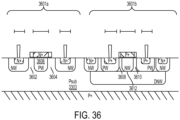
- such coupling beneficially reduces grating lobes of ultrasound waveforms generated by the ultrasonic transducer elements. Additionally, such coupling facilitates beneficial use of the total transducer area in some cases described below.
- the act of coupling comprises coupling the at least one ultrasonic transducer cell in the one of the at least two ultrasonic transducer elements with the at least one ultrasonic transducer cell in the other of the at least two ultrasonic transistor elements via a resistive element.
- the resistive element comprises a polysilicon resistor. Use of such resistors, and suitable selection of the resistance values, in some cases described below optimizes performance of the ultrasonic transducer elements.
- the act of coupling comprises coupling a first pair of ultrasonic transducer cells in different ones of the at least two ultrasonic transducer elements with a first coupling element having a first impedance value, and coupling a second pair of ultrasonic transducer cells in the different ones of the at least two ultrasonic transducer elements with a second coupling element having a second impedance value, which is different than the first impedance value.
- Suitable selection of the impedance values in some cases described below, optimizes performance of the ultrasonic transducer elements.
- the act of coupling comprises establishing an inductive coupling between the at least one ultrasonic transducer cell in the one of the at least two ultrasonic transducer elements and the at least one ultrasonic transducer cell in the other of the at least two ultrasonic transducer elements.
- the method further comprises an act of intermingling at least some of the ultrasonic transducer cells of the at least two ultrasonic transducer elements.
- each of the at least two ultrasonic transducer elements comprises one or more micromachined ultrasonic transducer cells.
- the use of such cells facilitates integration of the ultrasonic transducers with other components on a CMOS wafer, according to some cases described below.
- the method further comprises an act of apodizing at least some transducer cells in each of the at least two transducer elements.
- the act of apodizing comprises apodizing the at least one transducer cell in the one of the at least two ultrasonic transducer elements and the at least one transducer cell in the other of the at least two transducer elements.
- an ultrasound device comprising at least two ultrasonic transducer elements each comprising a plurality of ultrasonic transducer cells. At least one ultrasonic transducer cell in one of the at least two ultrasonic transducer elements is coupled to at least one ultrasonic transducer cell in another of the at least two ultrasonic transducer elements.
- such coupling beneficially reduces grating lobes of ultrasound waveforms generated by the ultrasonic transducer elements. Additionally, such coupling facilitates beneficial use of the total transducer area in some cases described below.
- the at least one transducer cell in the one of the at least two transducer elements is coupled to the at least one transducer cell in the other of the at least two transducer elements via a resistive element.
- the resistive element comprises a polysilicon resistor.
- one of the at least two transducer elements comprises at least first and second transducer cells
- the other of the at least two transducer elements comprises at least third and fourth transducer cells
- the first and third transducer cells are coupled via a first coupling element having a first impedance value
- the second and fourth transducer cells are coupled via a second coupling element having a second impedance value, which is different than the first impedance value.
- Suitable selection of the impedance values in some cases described below, optimizes performance of the ultrasonic transducer elements.
- the at least two transducer elements are configured and arranged such that an inductive coupling is established between the at least one transducer cell in the one of the at least two transducer elements and the at least one transducer cell in the other of the at least two transducer elements.
- At least some of the transducer cells of the at least two transducer elements are intermingled, which in some cases described below provides benefits in terms of beneficial use of the transducer element area.
- each of the at least two ultrasonic transducer elements comprises one or more micromachined ultrasonic transducer cells.
- the use of such cells facilitates integration of the ultrasonic transducers with other components on a CMOS wafer, according to some cases described below.
- At least one transducer cell in each of the at least two transducer elements is apodized. In some cases described below, the at least one transducer cell in the one of the at least two ultrasonic transducer elements and the at least one transducer cell in the other of the at least two transducer elements are apodized.
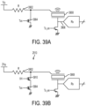
- a method for biasing an ultrasonic transducer element with a voltage comprising acts of using an output of a pulser to drive the ultrasonic transducer element so that the ultrasonic transducer element emits an ultrasonic pulse.
- the pulser may output a driving signal to one or more transducer elements corresponding to a generated waveform.
- the pulser is a circuit suitable to receive a waveform, for example from a waveform generator, and generate pulses (e.g., voltage pulses) to drive an ultrasonic transducer element.
- the output of the pulser may be applied as a bias signal to the ultrasonic transducer element.
- such operation may be used to provide safe high voltage biasing of transducer elements.
- an ultrasound device comprising at least one ultrasonic transducer element, and a pulser, coupled to the at least one ultrasonic transducer, configured and arranged such that, on at least some occasions when the at least one transducer element is being used to sense received ultrasonic energy, an output of the pulser is used to bias the at least one ultrasonic transducer element.
- a method for biasing at least one ultrasonic transducer element integrated on a semiconductor die comprising an act of biasing the at least one ultrasonic transducer element using a bias voltage applied to the semiconductor die.
- the method further comprises an act of applying a ground to a side of the at least one ultrasonic transducer element facing the subject while the at least one ultrasonic transducer element is being used to image or treat the subject.
- biasing in some cases described below, provides safe operation of the ultrasonic transducer element, minimizing risk of electric shock to the subject.
- an ultrasound device comprising at least one ultrasonic transducer element integrated on a semiconductor die.
- the at least one ultrasonic transducer element is configured and arranged on the die such that a bias voltage applied to the die is also used to bias the at least one ultrasonic transducer element.
- a bias voltage applied to the die is also used to bias the at least one ultrasonic transducer element.
- such a configuration is used to provide safe high voltage biasing of transducer elements.
- the ultrasound device is configured to image or treat a subject using the at least one ultrasonic transducer element.
- a side of the at least one ultrasonic transducer element that is configured to face the subject during imaging or treatment is connected to a ground, which provides for safe operation in some cases described below by minimizing the risk of electric shock.
- the at least one ultrasonic transducer element comprises one or more micromachined ultrasonic transducer cells.
- the one or more micromachined ultrasonic transducer cells comprise one or more capacitive micromachined ultrasonic transducer (CMUT) cells, and in some cases described below comprise one or more CMOS ultrasonic transducer (CUT) cells. The use of such cells facilitates integration of the ultrasonic transducers with other components on a CMOS wafer, according to some cases described below.
- CMUT capacitive micromachined ultrasonic transducer
- CUT CMOS ultrasonic transducer
- a method for biasing at least one ultrasonic transducer element comprising an act of applying a ground to a side of the at least one ultrasonic transducer element facing the subject while the at least one ultrasonic transducer element is being used to image or treat the subject.
- Such biasing facilitates safe operation of the device in some cases described below by minimizing the risk of electric shock.
- an ultrasound device is configured to image or treat a subject using at least one ultrasonic transducer element.
- a side of the at least one ultrasonic transducer element that is configured to face the subject during imaging or treatment is connected to a ground, which in some cases described below provides for safe operation by minimizing risk of electric shock.
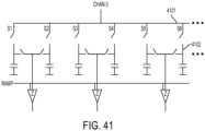
- a method for configuring first and second transmit control circuits in an ultrasound device, wherein each of the first and second transmit control circuits comprises a waveform generator that drives a pulser for an ultrasonic transducer element is provided, and wherein the method comprises an act of configuring the first and second transmit control circuits differently so that a length of a first delay between when the first control circuit receives a transmit enable signal and when a first waveform generated by the first waveform generator is applied to the first pulser is different than a length of a second delay between when the second control circuit receives the transmit enable signal and when a second waveform generated by the second waveform generator is applied to the second pulser.
- control of the delays provides beneficial operation, for example in terms of beneficial ultrasound imaging functions.
- the act of configuring the first and second transmit control circuits comprises acts of configuring the first transmit control circuit such that the transmit enable signal is delayed by a first amount of time before it reaches the first waveform generator, and configuring the second transmit control circuit such that the transmit enable signal is delayed by a second amount of time before it reaches the second waveform generator.
- the second amount of time is different than the first amount of time in some cases described below.
- the act of configuring the first and second transmit control circuits comprises acts of configuring the first waveform generator to have a first starting frequency, and configuring the second waveform generator to have a second starting frequency, which is different than the first starting frequency. In some cases described below, the act of configuring the first and second transmit control circuits comprises acts of configuring the first waveform generator to have a first starting phase, and configuring the second waveform generator to have a second starting phase, which is different than the first starting phase.
- the act of configuring the first and second transmit control circuits comprises acts of configuring the first transmit control circuit such that the first waveform output by the first waveform generator is delayed by a first amount of time before it reaches the first pulser, and configuring the second transmit control circuit such that the second waveform output by the second waveform generator is delayed by a second amount of time, which is different than the first amount of time, before it reaches the second pulser.
- such control facilitates generation of a variety of waveforms of interest, for example for use in ultrasound imaging as described herein.
- an ultrasound device comprising at least first and second ultrasonic transducer elements, a first transmit control circuit, and a second transmit control circuit.
- the first transmit control circuit comprises a first pulser coupled to the first ultrasonic transducer element so as to drive the first ultrasonic transducer element so that the first ultrasonic transducer element emits an ultrasonic pulse, a first waveform generator coupled to the first pulser to provide a first waveform to the first pulser in response to receipt of a transmit enable signal by the first transmit control circuit, and at least one first component may be included that impacts a length of a first delay between when the first transmit control circuit receives the transmit enable signal and when the first waveform is applied to the first pulser.
- the second transmit control circuit comprises a second pulser coupled to the second ultrasonic transducer element so as to drive the second ultrasonic transducer element so that the second ultrasonic transducer element emits an ultrasonic pulse, a second waveform generator coupled to the second pulser to provide a second waveform to the second pulser in response to receipt of the transmit enable signal by the second transmit control circuit, and at least one second component that impacts a length of a second delay between when the second transmit control circuit receives the enable signal and when the second waveform is applied to the second pulser.
- the at least one first component is configured differently than the at least one second component, so that the length of the second delay is different than the length of the first delay.
- the different delays provide beneficial operation, for example by facilitating generation of a variety of desirable ultrasound waveforms.
- the at least one first component comprises a first shift register that delays the enable signal by a first number of clock cycles before providing the enable signal to the first waveform generator
- the at least one second component comprises a second shift register that delays the enable signal by a second number of clock cycles, which is different than the first number of clock cycles, before providing the enable signal to the second waveform generator.
- the at least one first component comprises a first register containing a first value that determines a starting frequency of the first waveform generator
- the at least one second component comprises a second register containing a second value, which is different than the first value, that determines a starting frequency of the second waveform generator.
- the at least one first component comprises a first register containing a first value that determines a starting phase of the first waveform generator
- the at least one second component comprises a second register containing a second value, which is different than the first value, that determines a starting phase of the second waveform generator.
- the at least one first component comprises a first delay element that delays the first waveform output by the first waveform generator by a first amount of time before it reaches the first pulser
- the at least one second component comprises a second delay element that delays the second waveform output by the second waveform generator by a second amount of time, which is different than the first amount of time, before it reaches the second pulser.
- such configurations facilitate generation of a variety of beneficial ultrasound waveforms, for example by providing for control over waveform parameters.
- a method for configuring at least first and second waveform generators comprising an act of using a controller to control values of first and second configurable operational parameters of the at least first and second waveform generators.
- control makes the waveform generator(s) programmable, such that they may be programmed or controlled to provide desired waveforms, for example by controlling the waveform parameters.
- the method further comprises acts of generating a sequence of event numbers with the controller, for the first waveform generator, retrieving a first value associated with an event number provided by the controller from a first memory associated with the first waveform generator and providing the first value to the first waveform generator for use as the first configurable operational parameter.
- the method may further comprise, for the second waveform generator, retrieving a second value associated with the event number provided by the controller from a second memory associated with the second waveform generator and providing the second value to the second waveform generator for use as the second configurable operational parameter.
- the first and second configurable operational parameters control the same functionality of the first and second waveform generators.
- the first and second values retrieved from the first and second memories are different.
- the method further comprises an act of using the controller to transmit an enable signal to each of the first and second waveform generators.
- the method further comprises an act of setting the first and second configurable operational parameters of respective first and second waveform generators to have different values. In this manner, in some cases described below different waveforms are generated by the different waveform generators, which can be used to achieve desired ultrasound waveform generation, for instance in ultrasound imaging.
- a device comprising at least first and second waveform generators configured to generate waveforms for transmission by at least first and second corresponding ultrasonic transducer elements, the first waveform generator comprising at least one first configurable operational parameter and the second waveform generator comprising at least one second configurable operational parameter, and a controller configured to control values of the first and second configurable operational parameters.
- the controller is configured to output a sequence of transmit event numbers.
- the first waveform generator has associated therewith a first event memory that stores values for the first configurable operational parameter associated with respective transmit event numbers, and is configured to receive transmitted event numbers from the controller and to output corresponding stored values for the first configurable operational parameter to the first waveform generator for use thereby.
- the second waveform generator has associated therewith a second event memory that stores values for the second configurable operational parameter associated with respective transmit event numbers, and is configured to receive transmitted event numbers from the controller and to output corresponding stored values for the second configurable operational parameter to the second waveform generator for use thereby. In this manner, in some cases described below the waveforms generated by the waveform generators may be controlled, and desired waveforms may be achieved, for example when performing ultrasound imaging.
- the first event and second event memories store different associated values for the first and second configurable operational parameters.
- the controller is further configured to communicate a transmit enable signal to each of the first and second waveform generators.
- the first configurable operational parameter can be set to a different value than the second configurable operational parameter.
- a method for making an ultrasound device comprising an act of integrating digital receive circuitry on the same semiconductor die as at least one CMOS ultrasonic transducer element.
- the digital receive circuitry may be digital circuitry configured to receive signals from an ultrasonic transducer cell or element. Examples are described herein. In some cases described below, such configurations may provide or otherwise facilitate an integrated ultrasound device by allowing for ultrasonic transducers and digital circuitry to be on the same semiconductor die. Compact ultrasound devices result in some cases described below. Also, the digital circuitry facilitates digital communication with external components in some cases described below, such as external computers, smartphones, tablets, or other processing components.
- a device comprising at least one CMOS ultrasonic transducer element and digital receive circuitry formed on a single integrated circuit substrate.
- CMOS ultrasonic transducer element and digital receive circuitry formed on a single integrated circuit substrate.
- such configurations provide or otherwise facilitate an integrated ultrasound device by allowing for ultrasonic transducers and digital circuitry to be on the same semiconductor die.
- Compact ultrasound devices result in some cases described below.
- the digital circuitry facilitates digital communication with external components in some cases described below, such as external computers, smartphones, tablets, or other processing components.
- a method for making an ultrasound device comprising an act of fabricating at least first and second ultrasonic transducer elements above (e.g., on a higher or later provided processing layer) CMOS circuitry comprising at least first and second transmit control circuits and at least first and second receive control circuits corresponding to the first and second ultrasonic transducer elements.
- CMOS circuitry comprising at least first and second transmit control circuits and at least first and second receive control circuits corresponding to the first and second ultrasonic transducer elements.
- such fabrication facilitates formation of integrated ultrasound devices including ultrasonic transducers and associated circuitry.
- the devices may be compact due at least in part to positioning the ultrasonic transducers relative to the circuitry as described.
- the first and second receive control circuits each comprises an analog to digital converter, and in some cases described below further comprises digital signal processing circuitry. Inclusion of digital circuitry facilitates data processing and digital communication with external components, in some cases described below.
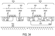
- the at least first and second ultrasonic transducer elements are fabricated above (e.g., on a higher or later provided processing layer) the CMOS circuitry such that the first transmit control circuit and the first receive control circuit are both disposed underneath the first ultrasonic transducer element, and the second transmit control circuit and the second receive control circuit are both disposed underneath the second ultrasonic transducer element.
- the circuit components may be underneath the ultrasonic transducers in the sense that they may be fabricated on processing layers completed prior to formation of the ultrasonic transducers, in some cases described below.
- the ultrasonic transducers are situated more closely to a device surface of a substrate (e.g., a semiconductor substrate) than are the circuits. In at least some cases described below, such configurations allow for compact ultrasound devices to be fabricated.
- the act of fabricating the at least first and second ultrasonic transducer elements comprises fabricating the at least first and second ultrasonic transducer elements on the same semiconductor substrate as the CMOS circuitry. In some cases described below, the act of fabricating the at least first and second ultrasonic transducer elements comprises acts of fabricating the first transmit control circuit so as to include a first waveform generator coupled to drive a first pulser for the first ultrasonic transducer element, and fabricating the second transmit control circuit so as to include a second waveform generator coupled to drive a second pulser for the second ultrasonic transducer element.
- An integrated ultrasound device is achieved in some cases described below, including signal generation functionality on the semiconductor substrate.
- an ultrasound device comprising at least first and second ultrasonic transducer elements, and CMOS circuitry disposed underneath the at least first and second ultrasonic transducer elements.
- the CMOS circuitry has integrated therein first and second transmit control circuits and first and second receive control circuits corresponding to the first and second ultrasonic transducer elements.
- such configurations facilitate formation of integrated ultrasound devices including ultrasonic transducers and associated circuitry.
- the devices may be compact due at least in part to positioning the ultrasonic transducers relative to the circuitry as described.
- the first and second receive control circuits each comprise an analog to digital converter. In some cases described below, the first and second receive control circuits each further comprises digital signal processing circuitry. Inclusion of digital circuitry facilitates data processing and digital communication with external components, in some cases described below.
- the first transmit control circuit and the first receive control circuit are both disposed underneath the first ultrasonic transducer element, and the second transmit control circuit and the second receive control circuit are both disposed underneath the second ultrasonic transducer element. In at least some cases described below, such configurations allow for compact ultrasound devices to be fabricated.
- the first and second ultrasonic transducer elements are integrated on the same semiconductor die as the CMOS circuitry, which in at least some cases described below facilitates fabrication of integrated ultrasound devices.
- the first transmit control circuit comprises a first waveform generator coupled to drive a first pulser for the first ultrasonic transducer element
- the second transmit control circuit comprises a second waveform generator coupled to drive a second pulser for the second ultrasonic transducer element
- each of the first and second ultrasonic transducer elements comprises one or more micromachined ultrasonic transducer cells.
- the one or more micromachined ultrasonic transducer cells comprise one or more capacitive micromachined ultrasonic transducer (CMUT) cells, and in some cases described below the one or more micromachined ultrasonic transducer cells comprise one or more CMOS ultrasonic transducer (CUT) cells.
- CMUT capacitive micromachined ultrasonic transducer
- CUT CMOS ultrasonic transducer
- a method for processing a signal from an ultrasonic transducer element comprising an act of, with a component integrated on the same semiconductor die as the ultrasonic transducer element, transmitting data corresponding to an output of the ultrasonic transducer element out of the semiconductor die as a high-speed serial data stream.
- Such operation in some cases described below facilitates communication of the data to external processing components, such as computers, smartphones, or tablets.
- the method further comprises an act of converting an analog signal corresponding to an output of the ultrasonic transducer element into a digital signal, and the act of transmitting data comprises transmitting data corresponding to the digital signal out of the semiconductor die as the high-speed serial data stream.
- Digital communication with external components is provided in some cases described below.
- the method further comprises an act of, with at least one additional component integrated on the semiconductor die, processing the digital signal to reduce the data bandwidth thereof, which is beneficial in some cases described below to facilitate further processing of the data and communication of the data to external component, such as computers, smartphones, and tablets.
- the at least one additional component comprises a digital quadrature demodulator.
- the at least one additional component comprises an averaging module.
- the at least one additional component comprises a matched filter, and in alternative cases described below comprises a mismatched filter.
- the at least one additional component comprises a finite impulse response (FIR) filter.
- FIR finite impulse response
- the at least one additional component comprises a 1 ⁇ 2 band decimating low-pass filter.
- the at least one additional component comprises a dechirp module.
- the method further comprises an act of, with at least one additional component integrated on the semiconductor die, prior to converting the analog signal into a digital signal, processing the analog signal to decouple waveforms therefrom. In some cases described below, such processing reduces an amount of data, which in turn facilitates collection and transmission of ultrasound data.
- the at least one additional component comprises an analog quadrature demodulator, and in some cases described below comprises an analog dechirp module.
- the act of transmitting comprises using a USB module to transmit the data corresponding to the output of the ultrasonic transducer element out of the semiconductor die as the high-speed serial data stream.
- the USB module comprises a USB 3.0 module.
- the act of transmitting comprises using a low voltage differential signal (LVDS) link to transmit the data corresponding to the output of the ultrasonic transducer element out of the semiconductor die.
- LVDS low voltage differential signal
- an ultrasound device comprising at least one ultrasonic transducer element integrated on a semiconductor die, and a high-speed serial data module, integrated on the semiconductor die, and configured to transmit data corresponding to an output of the ultrasonic transducer element out of the semiconductor die as a high-speed serial data stream.
- the high-speed serial data stream facilitates the use of the ultrasound device in connection with devices that can receive serial data streams, in some cases described below.
- the device further comprises an analog-to-digital (ADC) converter, integrated on the semiconductor die, configured to convert an analog signal corresponding to the output of the ultrasonic transducer element into a digital signal.
- ADC analog-to-digital
- the high-speed serial data module is configured to transmit data corresponding to the digital signal out of the semiconductor die as the high-speed serial data stream. In some cases described below, such operation facilitates communication of ultrasound data with external devices.
- the ultrasound device further comprises at least one signal processing module, integrated on the semiconductor die, and configured to process the digital signal to reduce the data bandwidth thereof, which is beneficial in some cases described below to facilitate further processing and communication to external components, such as computers, smartphones, and tablets.
- the at least one signal processing module comprises a digital quadrature demodulator.
- the at least one signal processing module comprises an averaging module.
- the at least one signal processing module comprises a matched filter, and in alternative cases described below comprises a mismatched filter.
- the at least one signal processing module comprises a finite impulse response filter.
- the at least one signal processing module comprises a 1 ⁇ 2 band decimating low-pass filter.
- the at least one signal processing module comprises a dechirp module.
- the device further comprises at least one additional component, integrated on the semiconductor die, and configured to process the analog signal to decouple waveforms therefrom before the ADC converter converts the analog signal into a digital signal.
- the at least one additional component comprises an analog quadrature demodulator, and in some cases described below comprises an analog dechirp module.
- the high-speed serial data module comprises a USB module.
- the USB module comprises a USB 3.0 module.
- the high-speed serial data module comprises a low voltage differential signal (LVDS) link module.
- LVDS low voltage differential signal
- a method for operating transmit and/or control circuits for at least first and second ultrasonic transducer elements integrated on the same semiconductor die as the transmit and/or control circuits comprising an act of using a controller to control values of operational parameters of the transmit and/or control circuits for the at least first and second ultrasonic transducer elements.
- control facilitates generation of desirable waveforms in some cases described below.
- the method further comprises an act of, with a controller that is not integrated on the semiconductor die, communicating the operational parameters to the registers associated with the transmit and/or control circuits via a high-speed serial data link.
- the act of using the controller comprises using the controller to control values of operational parameters of waveform generators of transmit control circuits for the at least first and second ultrasonic transducer elements. In some cases described below, the act of using the controller comprises using the controller to control values of operational parameters of amplifiers of receive control circuits for the at least first and second ultrasonic transducer elements.
- a device comprising at least first and second ultrasonic transducer elements integrated on a semiconductor die, transmit and/or control circuits, integrated on the semiconductor die, and a controller configured to control values of operational parameters of the transmit and/or control circuits for the at least first and second ultrasonic transducer elements.
- a configuration represents at least part of an integrated ultrasound device, such as an ultrasound imaging device configured to collect ultrasound data suitable for forming ultrasound images.
- the controller is not integrated on the semiconductor die and is configured to communicate the operational parameters to the registers associated with the transmit and/or control circuits via a high-speed serial data link. In some cases described below, the controller is configured to control values of operational parameters of waveform generators of transmit control circuits for the at least first and second ultrasonic transducer elements. In some cases described below, the controller is configured to control values of operational parameters of amplifiers of receive control circuits for the at least first and second ultrasonic transducer elements.
- a device comprising an ultrasound imaging chip, and a high intensity focused ultrasound (HIFU) chip.
- the ultrasound imaging chip and the HIFU chip are coupled to operate in combination to perform image-guided HIFU.
- the ultrasound imaging chip may include suitable components (e.g., ultrasonic transducers and circuitry) to collect ultrasound data suitable for forming ultrasound images.
- the HIFU chip may include suitable components (e.g., ultrasonic transducers and circuitry) to apply HIFU energy.
- images resulting from ultrasound data collected by the ultrasound imaging are used to guide application of HIFU by the HIFU chip.
- a device comprising a single chip integrated ultrasound imaging circuit and high intensity focused ultrasound (HIFU) circuit.
- the device is configured to perform image-guided HIFU.
- a single device is configured, in some cases described below, to perform multiple ultrasound functions.
- a device comprising an arrangement of ultrasound transducer elements on a CMOS wafer, an integrated circuit formed on the CMOS wafer and electrically coupled to the arrangement of ultrasound transducer elements.
- the integrated circuit is configured to drive a voltage up to approximately 50 V. Such voltage is beneficial in some cases described below for applying HIFU and/or performing ultrasound imaging, which can call for use of high voltages.
- the integrated circuit comprises a submicron node.
- the submicron node is configured to drive the voltage up to approximately 50 V.
- submicron nodes may refer to nodes that are smaller than approximately 1 micron.
- deep submicron nodes may refer to nodes that are smaller than approximately 0.3 microns.
- ultra-deep submicron nodes may refer to nodes that are smaller than approximately 0.1 micron.
- the ultrasonic transducer element may comprise one or more micromachined ultrasonic transducer cells.
- the one or more micromachined ultrasonic transducer cells comprise one or more capacitive micromachined ultrasonic transducer (CMUT) cells, and in some cases described below comprise one or more CMOS ultrasonic transducer (CUT) cells.
- CMUT capacitive micromachined ultrasonic transducer
- CUT CMOS ultrasonic transducer
- Some embodiments of the present disclosure provide new apparatuses, systems, and methods that leverage the benefits of CMUT technology and push the forefront of ultrasound image formation processing in ultrasonic scanners.
- a robust and highly integrated ultrasound "system on a chip" is provided with direct integration with ultrasonic transducer arrays fabricated on the same die as a fully digital ultrasound front-end.
- this architecture may allow sufficient access to fully digitized channel data to permit the use of state-of-the-art, off-the-shelf compute platforms for performing sophisticated image formation algorithms.
- CMOS complementary metal-oxide-semiconductor
- integrated circuitry uniquely enables this waveform generator to control a multi-level (e.g., 3 or more level) pulser and provides the capability to implement many advanced ultrasound techniques in subsequent processing - a feature that has not been previously achieved in a fully integrated transducer/CMOS configuration.
- ultrasound receiver architectures need to reduce the data bandwidth from multiple channels.
- One way to do this in conventional ultrasound is to use standard beamforming methods. This operation is irreversible and is not compatible with many more advanced ultrasound image reconstruction techniques.
- the full channel data rates may exceed the bandwidth of a system's external digital link.
- the integrated circuit detailed herein is uniquely designed for an integrated ultrasound imaging device.
- the CMOS contacts facilitate direct wafer bonding, sacrificial release, flip-chip bonding, and/or other techniques for establishing interconnections to ultrasound transducing elements.
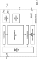
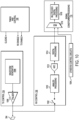
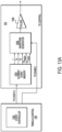
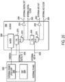
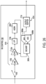
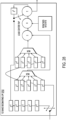
- Fig. 1 shows an illustrative example of a monolithic ultrasound device 100 embodying various aspects of the present invention.
- the device 100 includes one or more transducer arrangements (e.g., arrays) 102, a transmit (TX) control circuit 104, a receive (RX) control circuit 106, and may include a timing & control circuit 108, a signal conditioning/processing circuit 110, a power management circuit 118, and/or a high-intensity focused ultrasound (HIFU) controller 120.
- TX transmit
- RX receive
- HIFU high-intensity focused ultrasound
- the TX control circuit 104 and the RX control circuit 106 may be instead located off-chip, as discussed in more detail below.
- the illustrated example shows both a TX control circuit 104 and an RX control circuit 106, in alternative examples not covered by the claims (also discussed in more detail below) only a TX control circuit or only an RX control circuit may be employed.
- such examples not covered by the claims may be employed in a circumstance where one or more transmission-only devices 100 are used to transmit acoustic signals and one or more reception-only devices 100 are used to receive acoustic signals that have been transmitted through or reflected by a subject being ultrasonically imaged.
- one or more high-speed busses may be used to allow high-speed intra-chip communication or communication with one or more off-chip components.
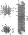
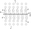
- the one or more transducer arrays 102 may take on any of numerous forms, and aspects of the present technology do not necessarily require the use of any particular type or arrangement of transducer cells or transducer elements. Indeed, although the term "array" is used in this description, it should be appreciated that in some embodiments the transducer elements may not be organized in an array and may instead be arranged in some non-array fashion.
- Each of the transducer elements in the array 102 includes one or more CMUTs.
- the transducer elements 304 of each transducer array 102 are formed on the same chip as the electronics of the TX control circuit 104 and RX control circuit 106.
- a CUT may, for example, include a cavity formed in a CMOS wafer, with a membrane overlying the cavity, and in some embodiments sealing the cavity. Electrodes may be provided to create a transducer cell from the covered cavity structure.
- the CMOS wafer may include integrated circuitry to which the transducer cell may be connected.
- the transducer cell and CMOS wafer may be monolithically integrated, thus forming an integrated ultrasonic transducer cell and integrated circuit on a single substrate (the CMOS wafer).
- the TX control circuit 104 generates pulses that drive the individual elements of, or one or more groups of elements within, the transducer array(s) 102 so as to generate acoustic signals to be used for imaging.
- the RX control circuit 106 receives and processes electronic signals generated by the individual elements of the transducer array(s) 102 when acoustic signals impinge upon such elements.
- the timing & control circuit 108 may, for example, be responsible for generating all timing and control signals that are used to synchronize and coordinate the operation of the other elements in the device 100.
- the timing & control circuit 108 is driven by a single clock signal CLK supplied to an input port 116.
- the clock signal CLK may, for example, be a high-frequency clock used to drive one or more of the on-chip circuit components.
- the clock signal CLK may, for example, be a 1.5625GHz or 2.5GHz clock used to drive a high-speed serial output device (not shown in Fig.
- timing & control circuit 108 may divide or multiply the clock CLK, as necessary, to drive other components on the die 112.
- two or more clocks of different frequencies may be separately supplied to the timing & control circuit 108 from an off-chip source.
- An illustrative example of a suitable clock generation circuit 1904 that may be included within the timing & control circuit 108 is discussed below in connection with Figs. 19 and 20 .
- the power management circuit 118 may, for example, be responsible for converting one or more input voltages V IN from an off-chip source into voltages needed to carry out operation of the chip, and for otherwise managing power consumption within the device 100.
- a single voltage e.g., 12V, 80V, 100V, 120V, etc.
- the power management circuit 118 may step that voltage up or down, as necessary, using a charge pump circuit or via some other DC-to-DC voltage conversion mechanism.
- multiple different voltages may be supplied separately to the power management circuit 118 for processing and/or distribution to the other on-chip components.
- a HIFU controller 120 may be integrated on the die 112 so as to enable the generation of HIFU signals via one or more elements of the transducer array(s) 102.
- a HIFU controller for driving the transducer array(s) 102 may be located off-chip, or even within a device separate from the device 100. That is, aspects of the present disclosure relate to provision of ultrasound-on-a-chip HIFU systems, with and without ultrasound imaging capability. It should be appreciated, however, that some embodiments may not have any HIFU capabilities and thus may not include a HIFU controller 120.
- the HIFU controller 120 may not represent distinct circuitry in those embodiments providing HIFU functionality.
- the remaining circuitry of FIG. 1 may be suitable to provide ultrasound imaging functionality and/or HIFU, i.e., in some embodiments the same shared circuitry may be operated as an imaging system and/or for HIFU. Whether or not imaging or HIFU functionality is exhibited may depend on the power provided to the system.
- HIFU typically operates at higher powers than ultrasound imaging.
- providing the system a first power level (or voltage) appropriate for imaging applications may cause the system to operate as an imaging system, whereas providing a higher power level (or voltage) may cause the system to operate for HIFU.
- Such power management may be provided by off-chip control circuitry in some embodiments.
- imaging and HIFU applications may utilize different waveforms.
- waveform generation circuitry may be used to provide suitable waveforms for operating the system as either an imaging system or a HIFU system.
- the system may operate as both an imaging system and a HIFU system (e.g., capable of providing image-guided HIFU).
- a HIFU system e.g., capable of providing image-guided HIFU.
- the same on-chip circuitry may be utilized to provide both functions, with suitable timing sequences used to control the operation between the two modalities. Additional details with respect to HIFU implementations and operational features that may be employed in the various embodiments set forth in the present disclosure are described in co-pending and co-owned U.S. Patent Application Serial No. 13/654,337 ( published as US 2014/066763 A2), entitled TRANSMISSIVE IMAGING AND RELATED APPARATUS AND METHODS, filed October 17, 2012 .
- one or more output ports 114 outputs a high-speed serial data stream generated by one or more components of the signal conditioning/processing circuit 110.
- Such data streams may, for example, be generated by one or more USB 3.0 modules, and/or one or more 10GB, 40GB, or 100GB Ethernet modules, integrated on the die 112.
- the signal stream produced on output port 114 can be fed to a computer, tablet, or smartphone for the generation and/or display of 2-dimensional, 3-dimensional, and/or tomographic images.
- an imaging device including an N ⁇ M planar or substantially planar array of CMUT elements may itself be used to acquire an ultrasonic image of a subject, e.g., a person's abdomen, by energizing some or all of the elements in the array(s) 102 (either together or individually) during one or more transmit phases, and receiving and processing signals generated by some or all of the elements in the array(s) 102 during one or more receive phases, such that during each receive phase the CMUT elements sense acoustic signals reflected by the subject.
- a subject e.g., a person's abdomen
- a single imaging device may include a P ⁇ Q array of individual devices, or a P ⁇ Q array of individual N ⁇ M planar arrays of CMUT elements, which components can be operated in parallel, sequentially, or according to some other timing scheme so as to allow data to be accumulated from a larger number of CMUT elements than can be embodied in a single device 100 or on a single die 112.
- a pair of imaging devices can be positioned so as to straddle a subject, such that one or more CMUT elements in the device(s) 100 of the imaging device on one side of the subject can sense acoustic signals generated by one or more CMUT elements in the device(s) 100 of the imaging device on the other side of the subject, to the extent that such pulses were not substantially attenuated by the subject.
- the same device 100 can be used to measure both the scattering of acoustic signals from one or more of its own CMUT elements as well as the transmission of acoustic signals from one or more of the CMUT elements disposed in an imaging device on the opposite side of the subject.
- FIG. 2A-B An illustrative example of an embodiment of an ultrasound unit 200 that is adapted to transmit acoustic signals and receive only pulses that are backscattered from a subject 202 is shown in Figs. 2A-B .
- the ultrasound unit 200 may, for example, comprise one or more devices 100 arranged in an array on a circuit board (not shown) and supported by a housing of the ultrasound unit 200.
- a high-speed serial data stream from the ultrasound unit 200 may be output to a serial port (e.g., a USB port) of a computer 204 for further processing and/or display on a screen 206 of the computer 204.
- a serial port e.g., a USB port
- the computer 204 may or may not be required to perform functions such as waveform removal, image formation, backend processing, etc., prior to displaying the image on the computer's display screen 206, depending on whether components for achieving such functionality are integrated on the die 112 of one or more of the devices 100, or are otherwise provided for in the ultrasound unit 200.
- the high-speed serial data stream from the ultrasound unit 200 may be provided to an input port of a smartphone 208 for further processing and/or display.
- some or all of the data processing e.g., waveform removal, image formation, and/or backend processing, etc.
- the data processing may be performed on the die 112 of one or more of the device(s) 100, or otherwise, within the ultrasound unit 200.
- some or all of such data processing may additionally or alternatively be performed by one or more processors on the smartphone 208.
- FIGs. 3A-B Another example of an implementation that employs a pair of opposing ultrasound units 200 is illustrated in Figs. 3A-B .
- a pair of ultrasound units 200 may be arranged so as to straddle a subject 202 (the ultrasound unit 200 behind the subject 202 is not visible in Fig. 3A ) and to output a serial stream of data to a desktop computer or workstation 306.
- Fig. 3B illustrates how transducer array(s) 102 of the device(s) 100 can be positioned so as to image a region 302 within the subject 202.
- the individual transducer elements 304 in a given array 102 can be used to generate acoustic signals or to receive acoustic signals, or both, depending on the imaging technique and methodology that is to be employed. Any of the foregoing examples may, for example, allow 2D brightness mode (B-mode), 3D B-mode, or tomographic ultrasonic imaging.
- B-mode 2D brightness mode
- 3D B-mode 3D B-mode
- tomographic ultrasonic imaging may, for example, allow 2D brightness mode (B-mode), 3D B-mode, or tomographic ultrasonic imaging.
- the devices and architectures disclosed herein may be fully integrated with one or more sophisticated methods, such as, for example, one or more synthetic aperture techniques.
- Synthetic aperture techniques may, for example, allow the formation of high-resolution imagery from multiple receive aperture collections. Examples of such techniques include, but are not limited to (1) transmit and receive on all pairs of transducer elements (2) plane wave compounding, (3) inverse scattering solutions for any transmit modes, (4) interpolation range migration (e.g., Stolt interpolation) or other Fourier resampling techniques, (5) dynamic focusing, (6) delay-and-sum, and (7) virtual sources.
- Fig. 4A shows an illustrative example of how an individual transducer element 304 in a transducer array 102 may be arranged with respect to CMOS circuitry 402 (including a TX control circuit 104 and an RX control circuit 106) for that transducer element 304.
- each transducer element 304 has associated with it a corresponding TX control circuit 104 and a corresponding RX control circuit 106. Details of example implementations of such circuits are described below.
- each of the transducer elements 304 is disposed directly above its corresponding TX control circuit 104 and RX control circuit 106 so as to, for example, facilitate interconnections, minimize cross-talk between components, minimize parasitic capacitances, etc.
- transducer cells e.g., transducer cells 602 described below
- transducer elements 304 and transducer array(s) 102 may be integrated with or otherwise formed above CMOS circuitry in this manner are provided in U.S. application serial No. 61/794,744 (published as US 2014/0264660 A1), entitled COMPLEMENTARY METAL OXIDE SEMICONDUCTOR (CMOS) ULTRASONIC TRANSDUCERS AND METHODS FOR FORMING THE SAME, bearing attorney docket No. B1348.70007US00 and filed on March 15, 2013 ).
- CMOS COMPLEMENTARY METAL OXIDE SEMICONDUCTOR
- one or more of the transducer elements 304 may be otherwise arranged with respect to one or more TX control circuits 104 and/or one or more RX control circuits 106, so as to achieve other benefits or advantages.
- some or all of the components of the TX control circuit 104 and/or the RX control circuit 106 may be omitted from the die 112, the device 100, and/or the ultrasound unit 200.
- the functionality of the TX control circuit 104 and/or the RX control circuit 106 may be performed by a different chip or even a different device, e.g., a computer.
- Fig. 4B shows an illustrative example of an ultrasound unit 200 comprising a group of individual ultrasound devices 100a-100d that can operate together under the direction of a controller 406.
- the ultrasound devices 100a-100d may be of the type described herein for device 100, may be an ultrasound-on-a-chip device in some embodiments, or may be other ultrasound devices.
- each of devices 100a-100d may be a single chip device including ultrasound transducers and integrated circuitry.
- the devices 100a-100d may be the same as each other or different types of devices.
- the devices 100a-100d may all provide the same functionality (e.g., ultrasound imaging functionality).
- one or more of the devices 100a-100d may be configured as ultrasound imaging devices and one or more may be configured as HIFU devices.
- one or more of the devices 100a-100d may be controllable to operate as either an imaging device or a HIFU device, or both.
- any number of individual devices 100 may be arranged in an array of two, four, eight, sixteen, or any other quantity, so as to form a larger area that can be used to emit and/or detect ultrasonic energy.
- the four illustrated devices 100a-100d represent a non-limiting example.
- the devices 100a-100d may be packaged within a common package or housing, may be disposed on a common substrate (e.g., a board or interposer), or may be mechanically coupled in any suitable manner.
- FIG. 19 An example of a clock generation circuit 1904 that may be included on the dies 112 of individual devices 100 in some embodiments so as to allow the operation of multiple devices 100a-100d to be synchronized is described below in connection with Figs. 19 and 20 .
- Fig. 5 illustrates how, in some embodiments, a single transducer element 304 may fit within a larger transducer array 102.
- Figs. 6A-E show five different examples of how a given transducer element 304 comprised of circular transducer cells 602 within an array 102 might be configured in some embodiments.
- each transducer element 304 in an array 102 may include only a single transducer cell 602 (e.g., a single CUT or CMUT).
- Figs. 5 illustrates how, in some embodiments, a single transducer element 304 may fit within a larger transducer array 102.
- Figs. 6A-E show five different examples of how a given transducer element 304 comprised of circular transducer cells 602 within an array 102 might be configured in some embodiments.
- each transducer element 304 in an array 102 may include only a single transducer cell 602 (e.g., a single CUT or CMUT).
- each transducer element 304 in an array 102 may include a group of individual transducer cells 602 (e.g., CUTs or CMUTs).
- Other possible configurations of transducer elements 304 include trapezoidal elements, triangular elements, hexagonal elements, octagonal elements, etc.
- each transducer cell 602 (e.g., CUT or CMUT) making up a given transducer element 304 may itself take on any of the aforementioned geometric shapes, such that a given transducer element 304 may, for example, include one or more square transducer cells 602, rectangular transducer cells 602, circular transducer cells 602, asterisk-shaped transducer cells 602, trapezoidal transducer cells 602, triangular transducer cells 602, hexagonal transducer cells 602, and/or octagonal transducer cells 602, etc.
- At least two of (e.g., all) of the transducer cells 602 within each given transducer element 304 act as a unit and together generate outgoing ultrasonic pulses in response to the output of the same pulser (described below) and/or together receive incident ultrasonic pulses and drive the same analog reception circuitry.
- the individual transducer cells 602 may be arranged in any of numerous patterns, with the particular pattern being chosen so as to optimize the various performance parameters, e.g., directivity, signal-to-noise ratio (SNR), field of view, etc., for a given application.
- an individual transducer cell 602 may, for example, be on the order of about 20-110 ⁇ m wide, and have a membrane thickness of about 0.5-1.0 ⁇ m, and an individual transducer element 304 may have a depth on the order of about 0.1-2.0 ⁇ m, and have a diameter of about 0.1mm-3mm, or any values in between.
- Figs. 7A-B show illustrative examples in which the transducer cells 602 (e.g., CUTs or CMUTs) of asterisk-shaped transducer elements 304 are intermingled
- Fig. 7C shows an illustrative example in which the transducer cells 602 of circular-shaped transducer elements 306 are intermingled, so as to achieve advantages such as the reduction of grating lobes.
- a similar effect of reducing grating lobes, etc. can be achieved, either in addition to or in lieu of intermingling transducer elements 304 in the array 102, by coupling one or more transducer cells 602 in a given transducer element 304 with one or more transducer cells 602 in one or more adjacent or nearby transducer elements 304.
- This cell sharing technique may, in some embodiments, be combined with an apodization technique in which some transducer cells 602 in a transducer element 304 are caused to radiate less power than other transducer cells 602 in the same element.
- transducer cells 602 e.g., CUTs or CMUTs
- the coupling elements 802 may, for example, comprise polysilicon resistors.
- the coupling elements 802 may additionally or alternatively comprise capacitive and/or inductive elements or features.
- inductive couplings may be created between pairs of transducer cells 602 by running conductors for to-be-coupled transducer cells 602 in close proximity to one another.
- certain transducer cells 602 e.g., the transducer cells 602 on the periphery of the shared transducer elements 304, may additionally be operated according to a desired apodization scheme.
- an apodization scheme may be applied to the transducer cells 602 that are coupled to the transduce cells 602 in other elements so that they radiate less power than the transducer cells 602 that are not so coupled.
- pairs of transducer cells 602 that are both located on the peripheries of two transducer elements 304 may be coupled together with an impedance value that is higher than the impedance value used to couple together pairs of transducer cells 602 for which one of the transducer cells 602 is not on the periphery of its transducer element 304. This possible configuration is illustrated in Fig. 9 .
- transducer cells 602a on the periphery of two transducer elements 304 may be coupled together via a coupling 802a (e.g., a polysilicon resistor) having a resistance value R1, whereas a transducer cell 602b closer to the center of a transducer element 304 may be coupled to another transducer cell 602 via a coupling 802b having a resistance value R2.
- the resistance value R2 may, for example, be greater than the resistance value R1.
- a gradient of impedance values may be employed that increases gradually from the periphery to the middle portion of a transducer element 304. Again, such a cell sharing technique employing different impedance values, or a gradient of impedance values, may be combined with an apodization technique so as optimize the performance of the array(s) 102 for a particular application.
- transducer elements 304 may have transducer cells 602 that are both intermingled and coupled together at their peripheries or via a gradient of impedance values, or otherwise.
- Fig. 10 is a block diagram illustrating how, in some embodiments, the TX control circuit 104 and the RX control circuit 106 for a given transducer element 304 may be used either to energize the transducer element 304 to emit an ultrasonic pulse, or to receive and process a signal from the transducer element 304 representing an ultrasonic pulse sensed by it.
- the TX control circuit 104 may be used during a "transmission” phase
- the RX control circuit may be used during a "reception" phase that is nonoverlapping with the transmission phase.
- one of the TX control circuit 104 and the RX control circuit 106 may simply not be used in a given device 100, such as when a pair of ultrasound units 200 is used for only transmissive imaging.
- a device 100 may alternatively employ only a TX control circuit 104 or only an RX control circuit 106.
- each TX control circuit 104 and each RX control circuit 106 are associated with a single transducer cell 602 (e.g., a CUT or CMUT), a group of two or more transducer cells 602 within a single transducer element 304, a single transducer element 304 comprising a group of transducer cells 602, a group of two or more transducer elements 304 within an array 102, or an entire array 102 of transducer elements 304.
- a single transducer cell 602 e.g., a CUT or CMUT
- a single transducer element 304 comprising a group of transducer cells 602, a group of two or more transducer elements 304 within an array 102, or an entire array 102 of transducer elements 304.
- the timing & control circuit 108 may be responsible for synchronizing and coordinating the operation of all of the TX control circuit 104/RX control circuit 106 combinations on the die 112, and the signal conditioning/processing circuit 110 may be responsible for handling inputs from all of the RX control circuits 106 (see element 1004 in Fig. 10 ) on the die 112.
- the timing & control circuit 108 may output either an "TX enable" signal to enable the operation of each TX control circuit 104, or an "RX enable” signal to enable operation of each RX control circuit 106.
- a switch 1002 in the RX control circuit 106 may always be opened before the TX control circuit 104 is enabled, so as to prevent an output of the TX control circuit 104 from driving the RX control circuit 106.
- the switch 1002 may be closed when operation of the RX control circuit 106 is enabled, so as to allow the RX control circuit 106 to receive and process a signal generated by the transducer element 304.
- the TX control circuit 104 for a respective transducer element 304 includes both a waveform generator 1006 and a pulser 1008.
- the waveform generator 1006 is responsible for generating a waveform that is to be applied to the pulser 1008, so as to cause the pulser 1008 to output a driving signal to the transducer element 304 corresponding to the generated waveform.
- the RX control circuit 106 for a respective transducer element 304 includes an analog processing block 1010, an analog-to-digital converter (ADC) 1012, and a digital processing block 1014.
- the ADC 1012 may, for example, comprise a 10-bit, 20Msps, 40Msps, or 80Msps ADC.
- the outputs of all of the RX control circuits 106 on the die 112 are fed to a multiplexer (MUX) 1016 in the signal conditioning/processing circuit 110.
- the MUX 1016 multiplexes the digital data from the various RX control circuits 106, and the output of the MUX 1016 is fed to a multiplexed digital processing block 1018 in the signal conditioning/processing circuit 110, for final processing before the data is output from the die 112, e.g., via one or more high-speed serial output ports 114. Examples implementations of the various circuit blocks shown in Fig. 10 are discussed further below.
- various components in the analog processing block 1010 and/or the digital processing block 1014 may serve to decouple waveforms from the received signal and otherwise reduce the amount of data that needs to be output from the die 112 via a high-speed serial data link or otherwise.
- one or more components in the analog processing block 1010 and/or the digital processing block 1014 may thus serve to allow the RX control circuit 106 to receive transmitted and/or scattered ultrasound pressure waves with an improved signal-to-noise ratio (SNR) and in a manner compatible with a diversity of waveforms.
- SNR signal-to-noise ratio
- the inclusion of such elements may thus further facilitate and/or enhance the disclosed "ultrasound-on-a-chip" solution in some embodiments.
- analog processing block 1010 Although particular components that may optionally be included in the analog processing block 1010 are described below, it should be appreciated that digital counterparts to such analog components may additionally or alternatively be employed in the digital processing block 1014. The converse is also true. That is, although particular components that may optionally be included in the digital processing block 1014 are described below, it should be appreciated that analog counterparts to such digital components may additionally or alternatively be employed in the analog processing block 1010.
- Fig. 11A illustrates a device 100 in which digital processing of a received signal is not performed on the die 112.
- this device may be essentially identical to that of Fig. 10 in terms of its basic structure and function, except that the RX control circuits 106 might not, for example, employ an ADC 1012 or a digital processing block 1014, and an on-chip signal conditioning/processing circuit 110 may be omitted.
- the RX control circuits 106 might not, for example, employ an ADC 1012 or a digital processing block 1014, and an on-chip signal conditioning/processing circuit 110 may be omitted.
- one or more buffers/drivers may additionally be employed to drive the analog signals onto output lines 1102a-b of the die 112.
- Fig. 11B illustrates an ultrasound device in which a waveform generator (not shown) and some or all of the other digital circuitry discussed herein may be located off-chip, rather than on the semiconductor die 112.
- this device may be otherwise identical to that of Fig. 10 in terms of its basic structure and functionality.
- the pulsers 1008 may additionally or alternatively be located off-chip.
- Fig. 12A shows an example of circuitry that may be included in each TX control circuit 104, in some embodiments, so as to allow for true time delay and amplitude control at every transmit location of the array(s) 102.
- the waveform generator 1006 is a chirp generator that includes a set of registers 1202a that can be set to control the characteristics of the chirp that is supplied to a tri-level pulser 1008. Specifically, a phase register " ⁇ 0 " controls the starting phase of the chirp, the frequency register "fo" controls the starting frequency of the chirp, and the chirp rate register "r" controls the rate at which the frequency of the chirp changes over time.
- the comparators 1204a-b serve to discretize the waveform signal output by accumulator 1206, so that the logical values D0, D1 supplied to the tri-level pulser 1008 are either "1,0,” “0,0,” or “0,1,” depending on comparisons of the output of the accumulator 1206 to the values V0 HIGH and V1 HIGH in the registers 1202a.
- Fig. 12B shows an alternative of the waveform generator 1006.
- a look up table 1212a is used to determine whether the output of accumulator 1206 is within a range defined by the values of V0 HIGH and V0 LOW in the registers 1202b
- a look up table 1212b is used to determine whether the output of accumulator 1206 is within a range defined by the values of V1 HIGH and V1 LOW in the registers 1202b.
- a tri-level pulser suitable for use as the pulser 1008 of Figs. 12A-B , as well as the benefits of employing such a pulser to drive a CMUT element, are described in Kailiang, C, "Ultrasonic Imaging Front-End Design for CMUT: A 3-Level 30Vpp Pulse-Shaping Pulser with Improved Efficiency and a Noise-Optimized Receiver," IEEE Asian Solid-State Circuits Conference," November 12-14, 2012/Kobe, Japan .
- the TX control circuit 104 is provided with three levels of control over the timing of the output of the pulser 1008.
- the coarsest level of timing control is provided by a shift register 1208 (which may be programmable, e.g., via the timing & control unit 108) located at the input of the waveform generator 1006.
- the next finest level of timing control is provided by the settings of the values " ⁇ 0 " and "fo" in the registers 1202a-b.
- delay lines 1210a-b may, for example, include PIN diodes that provide for delays on the order of about 72 picoseconds to 22 nanoseconds, or any delay value in between, though lesser and greater delays are also possible and contemplated.
- Examples of the waveform generator 1006 thus described allow for wideband or narrowband beamforming, coded excitation, e.g., Golay codes, Hadamard codes, Walsh codes, Cyclic Algorithm New (CAN) coding, azimuth phase coding, and/or other orthogonal waveforms, and/or may also allow the generation of gated continuous wave (CW) or impulse generation.
- coded excitation e.g., Golay codes, Hadamard codes, Walsh codes, Cyclic Algorithm New (CAN) coding, azimuth phase coding, and/or other orthogonal waveforms
- CW gated continuous wave
- Numerous additional examples of waveform generation techniques and options are described in co-pending and co-owned U.S. Patent Application Serial No. 13/654,337 , and will thus not be described further here.
- Fig. 13A shows an illustrative example of components that may be employed in the timing & control circuit 108 and each TX control circuit 104 to selectively determine values for the registers 1202a-b used by the waveform generator 1006 in the embodiments of Figs. 12A-B .
- each TX control circuit 104 may include an element event memory 1304 that stores values for the registers 1202a-b corresponding to each of several "TX event" numbers
- the timing & control circuit 108 may include an event controller 1302 that is responsible for communicating appropriate TX event numbers to each of the TX control circuits 104 on the die 112.
- the waveform supplied to each transducer element 304 in an array 102 can change from pulse to pulse, and by appropriately programming the event element memory 1304, complicated event sequencing, such as the excitation coding, e.g., Azimuth coding, mentioned above, focus/planewave scanning, etc., can be achieved.
- complicated event sequencing such as the excitation coding, e.g., Azimuth coding, mentioned above, focus/planewave scanning, etc., can be achieved.
- the excitation coding e.g., Azimuth coding, mentioned above, focus/planewave scanning, etc.
- Fig. 14 shows inputs and outputs for an event controller 1302 of the timing & control circuit 108 that may be provided, in some embodiments, so as to control both the transmission events and the receive events that occur in a ultrasound device 100.
- the event controller is provided with the parameters N TXSamples , N RXSamples , N TxEvents , and N RXEvents , and, when enabled via an enable signal "En,” generates and outputs TX and RX event numbers, as well as TX and RX enable signals, in response to an input clock "Clk.”
- Fig. 15A shows an illustrative example of a routine 1500 that may be performed by the event controller 1302 so as to generate a suitable sequence of outputs for controlling transmission and reception events.
- the flowchart on the left-hand side of Fig. 15A is an abstraction of the example routine illustrated by the flowchart on the right-hand side of that figure.
- the routine when the enable signal "En" is high, the routine alternates between performing a TX event subroutine 1502 and an RX event subroutine 1504, until the enable signal "En” transitions to low.
- the routine 1500 after being enabled, the routine 1500 first initializes the TX and RX event numbers to "0" (step 1506), and then proceeds with the TX event subroutine 1502a-c.
- the TX event subroutine 1502 causes the TX enable signal to be high for the number of samples specified by the N TXSamples parameter (step 1502b), and increments the TX event number by one (step 1502c) until the current TX event number exceeds the value of the N TXEvents parameter (step 1502a).
- the routine 1500 proceeds to the RX event subroutine 1504.
- the RX event subroutine 1504 causes the RX enable signal to be high for the number of samples specified by the N RXSamples parameter (step 1504b), and increments the RX event number by one (step 1504c) until the current RX event number exceeds the value of the N RXEvents parameter (step 1504a).
- the routine 1500 returns to the step 1506, at which the TX and RX event numbers are again initialized to "0," before beginning the TX subroutine 1502 once again.
- the event controller 1302 is able to interact with the TX control circuits 104 in a device 100 so that any number of the transducer elements 304 can fire a pulse at a time, and is able to interact with the RX control circuits 106 so that an acquisition window can be acquired in a specified manner.
- Possible operating modes of the event controller 1302 using the routine 1500 include (1) single transmit event/single receive event, (2) multiple transmit events/single receive event, (3) single transmit event/multiple receive events, and (4) multiple transmit events/multiple receive events.
- Fig. 13B shows another example of components that may be used to selectively determine values for one or more of the operational parameters used by the waveform generator 1006 of Figs. 12A-B (e.g., “ ⁇ ,” “fo,” “r,” “V0 LOW ,” “V0 HIGH ,” “V1 HIGH ,” and/or “V1 LOW ”) and/or values for one or more operational parameters for the RX control circuit 106, e.g., to control the LNA 1702, VGA 1704, etc. (discussed below in connection with Figs. 17 , 22 , 24 , 26 , 27 , 29 , and 30 ).
- Such values may, for example, be stored in a set of "next state” registers 1312a-b and a corresponding set of "current state” registers 1314a-b for each transducer element 304.
- a peripheral control module 1306, e.g., a USB 3.0 peripheral controller, may be integrated on the semiconductor die 112 so as to allow an external microprocessor 1308 to selectively communicate new values to the next state registers 1302 associated with some or all of the transducer elements 304 in an array 102.
- each group of state registers 1312, 1314 may be controlled by a corresponding register control module 1310a-b.
- the register control modules 1310a-b may be daisy chained from one register control module 1310 to the next.
- Fig. 15B shows an example of a routine 1508 that may be followed to selectively configure the registers 1312, 1314 in some embodiments.
- the microprocessor 1308 may, for example, receive an interrupt signal IRQ over the USB 3.0 link prior to each frame. Upon receiving such an interrupt, the microprocessor 1308 may determine whether the state of the current registers 1314 needs to be changed for the next event (see step 1510). If the microprocessor 1308 determines that the state should change, it may push a new complete sequence down the chain (see step 1512) and latch the new values into the next state registers 1312.
- the new values in the next state registers 1312 may then be latched into the current state registers 1302 on the frame boundary (see step 1514) for use in executing the next event (see steps 1516 and 1518).
- the above process may then be repeated to latch any desired new values into the next state registers 1312.
- Using such a technique to selectively control operational parameters of the TX control circuit 104 and/or the RX control circuit 106 may, for example reduce the required local memory requirements on the die 112, and may allow every pulse to have a unique definition with any arbitrary combination since the microprocessor 1308 may have fewer resource constraints than the sensor 102.
- Fig. 16 shows an alternative implementation of an ultrasound device 100 in which a single waveform generator 1006 may be shared by two or more TX control circuits 104.
- the shared waveform generator 1006 may, for example, be included in the timing & control circuit 108.
- delay elements 1602 may be disposed between the shared waveform generator 1006 and the respective pulsers 1008 in the TX control circuits 106, with the delay elements 1602 being selected so as to cause the output of the shared waveform generator 1006 to reach the respective pulsers 1008 according to a desired timing sequence.
- the delay elements 1008 may, for example, be located in the TX control circuits 104, in the timing & control circuit 108, or elsewhere. Using the illustrated technique, the transducer elements 304 of an array 102 may be pulsed according to any desired timing sequence, as determined by the delays provided by the respective delay elements 1602.
- Fig. 17 shows an illustrative example of components that may be included within the analog processing block 1010 and the digital processing block 1014 of each RX control circuit 106 (see Fig. 10 ).
- the components of the RX control circuit 106 may, for example, collectively have a bandwidth from DC to 50MHz and provide a gain of 50dB, with a noise figure of less than 4dB, aliased harmonic rejection of 45dB, and channel isolation of 40dB.
- Such parameters are listed for illustrative purposes only and are not intended to be limiting. Other performance parameters are possible and contemplated.
- the analog processing block 1010 may, for example, include a low-noise amplifier (LNA) 1702, a variable-gain amplifier (VGA) 1704, and a low-pass filter (LPF) 1706.
- the VGA 1704 may be adjusted, for example, via a time-gain compensation (TGC) circuit 1902 (shown in Fig. 19 ) included in the event controller 1302 of the timing & control circuit 108.
- TGC time-gain compensation
- the LPF 1706 provides for anti-aliasing of the acquired signal.
- the LPF 1706 may, for example, comprise a 2 nd order low-pass filter having a frequency cutoff on the order of 5MHz.
- the ADC 1012 may, for example, comprise a 10-bit, 20Msps, 40Msps, or 80Msps ADC.
- the digital control block 1014 of the RX control circuit 106 includes a digital quadrature demodulation (DQDM) circuit 1708, an averaging circuit 1714 (including an accumulator 1710 and an averaging memory 1712), and an output buffer 1716.
- the DQDM circuit 1708 may, for example, be configured to mix down the digitized version of the received signal from center frequency to baseband, and then low-pass filter and decimate the baseband signal.
- An illustrative example of a quadrature demodulation circuit that may be employed as the DQDM 1708 is shown in Fig. 18 .
- the DQDM 1708 may, for example, include a mixer block 1802, a low-pass filter (LPF), and a decimator circuit 1806.
- the illustrated circuit may allow for a lossless reduction of bandwidth by removing unused frequencies from the received signal, thus significantly reducing the amount of digital data that needs to be processed by the signal conditioning/processing circuit 110 and offloaded from the die 112.
- the bandwidth reduction achieved by these components may help to facilitate and/or improve the performance of the "ultrasound-on-a-chip" embodiments described herein.
- averaging block 1714 in the embodiment shown (including accumulator 1710 and averaging memory 1712) functions to average received windows of data.
- Fig. 19 shows an example implementation of the timing & control circuit 108.
- the timing & control circuit 108 may include both a clock generation circuit 1904, and an event controller 1302.
- the clock generation circuit 1904 may be used, for example, to generate some or all of the clocks used throughout the device 100.
- An example implementation of the clock generation circuit 1904 is shown in Fig. 20 .
- an external circuit 2002 may be used to generate a high-speed (e.g., 1.5625GHz) clock, e.g., using an oscillator 2004 and a phase lock loop (PLL) 2006, that can be fed to the clock generation circuit 1904.
- PLL phase lock loop
- the clock may be stepped down (e.g., via frequency divider circuit 2010) to a first frequency for use for clocking certain components on the die 112, and may be further stepped down (e.g, via frequency divider circuit 2016) to a second frequency for use by other components on the die 112.
- the frequency divider circuit 2010 may divide the 1.5625GHz clock so as to yield a 40MHz clock on the clock line 2022 for use within the die 112
- the frequency divider circuit 2016 may further divide the 40MHz clock so as to yield a 20MHz clock on the clock line 2024 for use within the die.
- the die 112 may have terminals 2026, 2028 connected to inputs of multiplexers 2012, 2018, respectively, to accept clock signals from external sources, and may additionally have output terminals 2030, 2032 connected to the outputs of the multiplexers 2012, 2018, respectively, to allow clock signals to be fed off-chip.
- this configuration can allow multiple chips to be synchronized by daisy chaining clocks.
- this technique allows multiple devices 100 to be extended into a fully synchronized, coherent M ⁇ N array of devices 100 that can operate as a unit to image a subject.
- the event controller 1302 may additionally comprise a TGC circuit 1902 that may be used, for example, to control the gain of the VGAs 1704 in the analog processing blocks 1010 of the RX control circuits 106.
- Fig. 21 shows an illustrative example of components that may be included in the multiplexed digital processing block 1018 of the signal conditioning/processing circuit 110 on the die 112.
- the multiplexed digital processing block 1018 may, for example, include a re-quantizer 2102 and a USB 3.0 module 2104.
- the re-quantizer 2102 may, for example, perform lossy compression to provide bandwidth reduction.
- the re-quantizer 2102 may operate in any of numerous ways, and aspects of the present technology do not necessarily require the use of any particular type of re-quantization technique.
- the re-quantizer 2102 may, for example, find a maximum magnitude of the incoming signal, scale all signals up to make the maximum signal full-scale, and then throw away the lower N-bits from the signal. In other embodiments, the re-quantizer 2102 may additionally or alternatively covert the signal to log space and keep only N bits of the signal. In yet other embodiments, the re-quantizer 2102 may additionally or alternatively employ Huffman coding and/or vector quantization techniques.
- USB 3.0 module one option for outputting a high-speed serial data stream from the die 112 is a USB 3.0 module. Details as to the structure and operation of such a USB 3.0 module are described, for example, in the Universal Serial Bus Revision 3.0 Specification, available at http://www.usb.org.
- Fig. 21 illustrates the use of a USB 3.0 module to provide a high-speed serial data stream from the chip, it should be appreciated that other data output techniques may additionally or alternatively be employed. For example, one or more 10GB, 40GB, or 100GB Ethernet modules may additionally or alternatively be employed. In other embodiments, other high-speed parallel or high-speed serial data output modules and/or techniques may additionally or alternatively be employed.
- Fig. 22 shows an example implementation of the RX control circuit 106 that includes a matched filter 2202 that may, for example, perform waveform removal and improve the signal-to-noise ratio of the reception circuitry.
- the filter circuit 2202 may actually operate as either a matched filter or a mismatched filter so as to decouple waveforms from the received signal.
- the matched filter 2202 may work for either linear frequency modulated (LFM) or non-LFM pulses.
- LFM linear frequency modulated
- the matched filter 2202 may, for example, include a padding circuit 2302, a fast Fourier transformation (FFT) circuit 2304, a multiplier 2306, a low-pass filter 2308, a decimator circuit 2310, and an inverse FFT circuit 2312.
- the padding circuit 2302 may, for example, apply padding to the incoming signal sufficient to avoid artifacts from an FFT implementation of circular convolution.
- the value of "H( ⁇ )" applied to the multiplier 2306 should be a conjugate of the transmission waveform T x ( ⁇ ).
- the filter 2202 may thus indeed operate as a "matched” filter, by applying a conjugate of the transmission waveform T x ( ⁇ ) to the multiplier 2306.
- the "matched” filter 2202 may instead operate as a mismatched filter, in which case some value other than a conjugate of the transmission waveform T x ( ⁇ ) may be applied to the multiplier 2206.
- Fig. 24 shows another example implementation of the RX control circuit 106.
- the RX control circuit 106 includes a dechirp circuit 2402 that can perform yet another technique to reduce bandwidth by isolating signals of interest. Dechirp circuits as also sometimes referred to as "digital ramp" or “stretch” circuits.
- a dechirp circuit 2402 may be included within the analog processing block 1010, or may be included within the digital processing block 1014 of the RX, or may be included in both the analog processing block 1010 and the digital processing block 1014 of the RX control circuit 106. Using a dechirp circuit with an LFM waveform effectively converts time to frequency.
- a digital dechirp circuit 2402 is shown in Fig. 25 .
- the dechirp circuit 2402 may include a digital multiplier 2502, a digital low pass filter 2504, and a decimator circuit 2506.
- Analog dechirp circuit - discussed below in connection with Fig. 26 - would employ an analog multiplier and filter, rather than a digital multiplier and filter, and would not include the decimator circuit 2506).
- the "reference chirp" shown in Fig. 25 may, for example, be the same "chirp" as that generated by the waveform generator 1006 in the corresponding TX control circuit 104.
- Fig. 26 shows yet another example implementation of an RX control circuit 106.
- an analog quadrature demodulation (AQDM) circuit 2602 and an analog dechirp circuit 2604 are included in the analog processing block 1010.
- the AQDM 2602 may, for example, employ an analog mixer (not shown) and a local oscillator (not shown) to mix the incoming signal to baseband and then employ a low-pass analog filter (not shown) to remove unwanted frequencies from the analog signal.
- an analog mixer not shown
- a local oscillator not shown
- a low-pass analog filter not shown
- two ADCs 2606a-b may be employed in this embodiment to convert the output of the analog dechirp circuit 2604 into a digital signal format, but each of the ADCs 2606a-b may run at half the rate as the ADC 1012 employed in the other examples, thus potentially reducing power consumption.
- a low-pass filter 2702 and multiplexer 2704 are included in the digital processing block 1014, together with an averaging block 1714.
- the low-pass filter 2702 may, for example, include a 1 ⁇ 2 band decimating finite impulse response (FIR) filter, and its operation may be configured to minimize the number of non-zero taps.
- FIR finite impulse response
- each RX control circuit 106 may use any of the foregoing analog and digital circuit elements either alone or in combination with any of the other described circuit elements, and aspects of the present technology do not necessarily require the specific configurations and/or combinations illustrated herein.
- each RX control circuit 106 may, in some embodiments, include any one or more of an AQDM 2602, an analog dechirp circuit 2604, a DQDM 1708, a matched and/or unmatched filter 2202, a digital dechirp circuit 2402, an averaging block 1714, and a low-pass filter 2702, in any combination and in any order with respect to the other components, provided analog-to-digital and/or digital-to-analog conversion is performed, as necessary.
- the use of any or all of the above-described bandwidth reduction techniques may, for some embodiments, help make the "ultrasound-on-a-chip" designs described herein a practical, viable, and commercially feasible solution.
- Fig. 29 illustrates an example of a novel technique for biasing the transducer elements 304 in an array 102.
- the side of each of the transducer elements 304 that faces the patient may be connected to ground, so as to minimize risk of electric shock.
- the other side of each transducer element 304 may be connected to the output of the pulser 1008 via a resistor 2902. Accordingly, each transducer element 304 is always biased via the output of the pulser 1008, regardless of whether the switch S1 is open or closed.
- the bias voltage applied across the element may be on the order of 100V.
- the switch S1 may be closed during a transmit operation and may be open during a receive operation.
- the switch S2 may be closed during a receive operation and may be open during a transmit operation. (Note that there is always a gap between the opening of switch S1 and the closing of switch S2, as well as between the opening of switch S2 and the closing of switch S1, so as to ensure the pulser 1008 does not apply an outgoing pulse to the LNA 1702 in the RX control circuit 106.)
- the pulser 1008 may hold the bottom plate of the transducer element 304 at its high output level at all times except when it is applying a waveform pulse to its transducer element 304, and the waveform pulse applied during the transmit phase may be referenced from the high output level of the pulser 1008. Accordingly, each individual pulser 1008 is able to maintain an ideal bias on its corresponding transducer element 304 at all times.
- a capacitor 2904 may be placed between the switch S2 and the LNA 1702 of the RX control circuit 106 so as to block the DC bias signal (i.e., the high output of the pulser 1008) from reaching the LNA 1702 during receive operations (i.e., when switch S2 is closed).
- Biasing the transducer elements 304 via their respective pulsers 1008 may provide benefits in some embodiments, such as reducing cross-talk that would otherwise occur if the elements 304 were biased via a common bus, for example.
- Fig. 30 shows another illustrative example of a technique for biasing the transducer elements 304 in an array 102.
- the side of the transducer element 304 facing the patient may be grounded, and a switch S1 may be positioned between the output of the pulser 1008 and the other side of the transducer element 304.
- a switch S2 in this case may be positioned directly between the non-grounded side of the transducer element 304 and the LNA 1702 of a RX control circuit 106.
- a capacitor is not positioned between the switch S2 and the LNA 1702, thus resulting in a potentially significant savings of real estate on the die 112 that would otherwise be consumed by such capacitors.
- one of the two switches i.e., either switch S1 or switch S2 may always be closed.
- switch S1 In transmit mode, switch S1 may be closed and switch S2 may be open. Conversely, in receive mode, switch S2 may be open and switch S1 may be closed.
- the entire die 112 (except for the portion that is used to bias the other side of the transducer elements 304, e.g., the top metal layer of the transducer array 102) may be biased at an optimal bias voltage for the transducer elements 304.
- This arrangement may thus facilitate safe high-voltage biasing of the transducer elements 304 via both the pulsers 1008 and the LNAs 1702 at all times.
- the power supply of the chip may be floated so that it is not grounded, and some or all of the control, configuration, and communication inputs/outputs to the die 112 can be isolated, e.g., using optical isolation techniques or appropriately sized capacitors, thus DC blocking the high-voltage from leaving the chip.
- Fig. 31 shows an illustrative example of components that may be included in the multiplexed digital processing block 1018 of the signal conditioning/processing circuit 110 on the die 112, in addition to or in lieu of the components discussed above in connection with Fig. 10 .
- one or more of the illustrated components may be integrated on the die 112, together with some or all of the other circuitry described herein, provided a sufficiently small process is used for the CMOS or other integrated circuit fabrication methodology that is employed to fabricate the die 112.
- the signal conditioning/processing circuitry 110 includes a re-quantizer module 2102, a waveform removal circuit and/or software 3102, an image formation circuit and/or software 3104, a backend processing circuit and/or software 3106, and a USB 3.0 module 2104.
- a re-quantizer module 2102 As the re-quantizer module and USB 3.0 module, and alternatives thereto, were discussed above in connection with Fig. 21 , those components will not be described further here.
- one or more processors 3108 may be integrated on the die 112, together with the other circuitry discussed above, so as to enable some or all of the waveform removal functionality, image formation functionality, and/or backend processing functionality, as described below, to be implemented via software routines executed by such components, as well as to achieve other functionality of the other components of the device 100 described above.
- the waveform removal module 3102, image formation module 3104, and/or backend processing module 3106 shown in Fig. 31 may be implemented partially or entirely via software stored in memory either on the die 112 or in one or more off-chip memory modules.
- one or more high-speed buses 3110 such as those used by a unified Northbridge chip, or similar components may be employed to allow high-speed data exchange among the processors(s) 3108, memory modules, and/or other components either located on the die 112 or disposed at some off-chip location.
- some or all of such functionality of the image formation module 3104, and/or backend processing module 3106 may additionally or alternatively be performed using one of more dedicated circuits integrated on the die 112.
- the waveform removal circuit and/or software 3102 may, for example, contain circuitry and/or software, similar to that discussed above in connection with the RX control circuits 106, to perform deconvolution of the waveform, dechirping, FFTs, FIR filtering, matched filtering and/or mismatched filtering, etc. Any or all of the foregoing functionality may be performed, either alone or together with any of the other functionality, in any order, by the waveform removal circuit and/or software 3102 on the die 112. Alternatively, in some embodiments, such waveform removal circuit and/or software 3102 may be separate from the die 112 but co-located with the die 112 in an ultrasound unit 200 and the same circuit board and/or in the same housing.
- the image formation circuit and/or software 3104 may, for example, contain circuitry and/or software configured to perform apodization, back projection and/or fast hierarchy back projection, interpolation range migration (e.g., Stolt interpolation) or other Fourier resampling techniques, dynamic focusing techniques, and/or delay and sum techniques, tomographic reconstruction techniques, etc. Any or all of the foregoing functionality may be performed, either alone or together with any of the other functionality, in any order, by the image formation circuit and/or software 3104 on the die 112. In some embodiments, the image formation circuit and/or software 3104 and the waveform removal circuit and/or software 3102 may both be located on the die 112.
- such image formation circuit and/or software 3104 and/or the waveform removal circuit and/or software 3102 may be separate from the die 112 but co-located with the die 112 in an ultrasound unit 200 and the same circuit board and/or in the same housing.
- the backend processing circuit and/or software 3106 on the die 112 may, for example, contain circuitry and/or software configured to perform down-range and/or cross-range autofocusing, frequency dispersion compensation, non-linear apodization, remapping, compression, denoising, compounding, Doppler, elastography, spectroscopy, and/or basis pursuit techniques, etc. Any or all of the foregoing functionality may be performed, either alone or together with any of the other functionality, in any order, by the back-end processing circuit and/or software 3106 on the die 112.
- the backend processing circuit and/or software 3106, the image formation circuit and/or software 3104, and/or the waveform removal circuit and/or software 3102 may all three be located on the die 112.
- such backend processing circuit and/or software 3106, image formation circuit and/or software 3104, and/or the waveform removal circuit and/or software 3102 may be separate from the die 112 but co-located with the die 112 in an ultrasound unit 200 and the same circuit board and/or in the same housing.
- memory used to achieve some or all of the above-described functionality may be located on-chip, i.e., on the die 112. In other embodiments, however, some or all of the memory used to implement some or all of the described functionality may be located off-chip, with the remainder of the circuitry, software, and/or other components being located on the die 112.
- the timing & control circuit 110 may include a set of externally-writable registers containing values for the parameters N TXSamples , N TXEvents , N RXSamples , and/or N RXEvents discussed above in connection with Figs. 14 and 15 ; the registers 1202 of the TX control circuits 104 discussed above in connection with Figs.
- 12A-B may be selectively programmed via one or more input ports; operational parameters of one or more of the components of the RX control circuit 106 discussed above in connection with Figs. 17 , 18 , and 22-28 may be selectively programmed via one or more input ports; operational parameters for one or more of the re-quantizer circuit 2102 and/or USB 3.0 circuit 2104 or other modules discussed above in connection with Fig. 21 may be programmed via one or more input ports; and/or operational parameters for one or more of the waveform removal circuit 3102, image formation circuit 3104, and/or backend processing circuit 3106 discussed above in connection with Fig. 31 may be programmed via one or more input ports.
- Figs. 32A-B illustrate embodiments in which some or all of the waveform removal circuit and/or software 3102, the image formation circuit and/or software 3104, and/or the backend processing circuit and/or software 3106 may be located off-chip, e.g., on a computing device 3202, 3206 separate from the device 100.
- a computing device 3202 not including one or more field-programmable gate arrays (FPGAs) 3208
- waveform removal may be performed by software executed by the processor 3204 of the computing device 3202, together with image formation and backend processing functions.
- waveform processing functionality may be performed by the FPGA(s) 3208 in addition to or in lieu of the processor 3204 of the computing device 3206 performing such functionality.
- ultrasonic transducer elements may be used for ultrasound imaging applications, HIFU, or both. It should be appreciated that such elements may operate at voltages higher than those conventionally used for CMOS integrated circuitry, e.g., higher than voltages typically supported by deep submicron CMOS circuitry. For example, such ultrasonic transducer elements may operate at voltages between 20 V and 120 V, between 30 V and 80 V, between 40 V and 60 V, at any voltage within those ranges, or at any other suitable voltages. HIFU applications may utilize higher voltages than ultrasound imaging applications.
- ultrasonic transducer elements with circuitry on a single chip may be facilitated by making such circuitry compatible with higher voltages than traditionally used for CMOS integrated circuitry, i.e., by operating standard CMOS deep submicron circuitry at higher than customary voltages.
- CMOS circuits There are two main issues that can limit the operating voltage of NMOS and PMOS devices in CMOS circuits: (1) gate oxide breakdown, and (2) source and drain (diffusion) breakdown.
- diffusion breakdown is the first limitation, in that the diffusion is specifically engineered in field effect transistors (FETs) to break down before the gate oxide so as to protect the gate oxide.
- FETs field effect transistors
- the relative concentrations in the source/drain regions to the substrate should be adequate. In some embodiments, lower doping levels in the source and drain regions may increase breakdown voltage.
- CMOS circuits can be implemented at the level of mask logic operations and device layout.
- the standard diffusion junction in NMOS technologies is N+ degenerately doped to P-well retrograde doped typically on the order of 10 17 to 10 18 dopants/cm 3 .
- a 3V device typically breaks down at 6 volts.
- the source and drain may, for example, be defined by the same implant that dopes the poly-Si gate. This is generally called a self-aligned transistor.
- the standard gate-to-drain interface is a Lightly Doped Drain (LDD).
- LDD Lightly Doped Drain
- the LDD may, for example, be doped to reduce the electric field but may be minimized in size in order to keep device length large enough to maintain gate control.
- CMOS circuitry may, for example, be turned into high-voltage CMOS circuitry by changing the diffusion scheme.
- a mask-aligned source and drain using N-well and P-well regions may be employed.
- the diffusion may be changed to N-well source/drain with P-substrate.
- the diffusion may be changed to P-well source/drain regions with N-Well and Deep N-well.
- the source and drains may be defined by Shallow Trench Isolation (STI). Alternatively, for larger voltages, the source and drains may be defined by gap space and thermal diffusion.
- circuit layouts and associated structures that may be used to implement high-voltage CMOS circuits in the various embodiments set forth in this disclosure are shown in Figs. 33-42 .
- Fig. 33 shows an example of a high voltage NMOS 3301a and PMOS 3301b layout that may be used in some embodiments, for example to provide high voltages a deep submicron nodes.
- the reference numerals set forth in Fig. 33 correspond to the following features and/or characteristics of the illustrated layout: 3302 - Large junction breakdown due to N-well (NW)/P-substrate (Psub 3303); 3304 - Reduced E-field due to LDD; 3306 - Large junction breakdown due to P-well (PW)/NW; and 3308 - Reduced E-field due to LDD.
- Fig. 34 shows an example of a very high voltage NMOS 3401a and PMOS 3401b layout that may be used in some embodiments.
- the reference numerals set forth in Fig. 34 correspond to the following features and/or characteristics of the illustrated layout: 3402 - Mask defined doping for N+ implant; 3404 - Thermally diffused PW/Psub; 3406 - Thermally diffused NW/Psub; 3408 - Mask defined doping for P+ implant; 3410 - Thermally diffused NW/Psub; and 3412 - Thermally diffused PW/Psub.
- Fig. 35 shows an example of a high voltage NMOS 3501a and PMOS 3501b bidirectional or cascoding layout that may be used in some embodiments.
- the reference numerals set forth in Fig. 35 correspond to the following features and/or characteristics of the illustrated layout: 3502 - N-well source and source gate extension; 3504 - N-well drain and gate extension; 3506 - P-Well source and source gate extension; and 3508 - P-well drain and gate extension.
- Fig. 36 shows an example of a very high voltage NMOS 3601a and PMOS 3601b bidirectional or cascoding layout that may be used in some embodiments.
- the reference numerals set forth in Fig. 36 correspond to the following features and/or characteristics of the illustrated layout: 3602, 3604 - Thermally diffused source and drain in Psub; 3606 - Optional P-well gate implant for threshold increase; 3608, 3610 - Thermally diffused source and drain in Psub; and 3612 - Optional N-well gate implant for threshold increase.
- Fig 37 shows an example of a pulser using a high voltage NMOS and PMOS layout with a high voltage switch that may be used in some embodiments.
- 3708 represents an Enable switch for receive an enable signal rx_en to isolate from high voltage.
- the transistors may have thick channels as illustrated by the thick gate lines in the figure, which signifies a high voltage (HV) device.
- HV high voltage
- Figs. 38A and 38B show examples of a double and quadruple voltage pulse drivers, respectively, that may be used in some embodiments.
- Figs. 39A-B show an example of a pulser that does not employ a receive isolation switch, which may be used in some embodiments.
- the reference numerals set forth in Fig. 39A-B correspond to the following features and/or characteristics of the illustrated layout: 3902 - Resistor defined by N-well in Psub or by nonsilicided polysilicon on FOX; 3904 - High-voltage NMOS pull down device; 3906 - Direct connection to RX (no switch yields less parasitics); 3908 - Automatic receive bias; and 3910 - Cascode device for double voltage.
- Figs. 40A and 40B show an example of a time-interleaved single slope ADC and the operation thereof, respectively, that, in some embodiments, may be employed as one or more of the ADCs reference herein.
- N parallel ADCs are used for one channel to take alternating samples such that the sampling frequency of each ADC is much lower than the Nyquist criterion.
- Such single slope ADCs may, for example, allow large-scale sharing of resources: bias, ramp, and gray counter. Such an ADC approach may thus provide a highly scalable, low power option.
- Fig. 41 shows an example of a time interleaved sample and hold circuit that may be employed in some embodiments.
- reference numeral 4102 signifies a step during which evens are sampled, and then odds are sampled
- reference numeral 4104 signifies a step during which the odds are compared, and then the evens are compared.
- Figs. 42A and 42B show an example of a time shared high speed ADC and the operation thereof, respectively, that, in some embodiments, may be employed as one or more of the ADCs referenced herein.
- Such an ADC may, for example, employ a pipelined, SAR, or flash architecture. Because a single high speed ADC having such an architecture may be used to sample N channels, such an ADC approach may significantly reduce area requirements.
- the high voltage CMOS circuitry described herein may be configured to drive voltages higher than those conventionally attainable with CMOS circuitry, and to provide high voltages at deep submicron nodes.
- voltages up to approximately 10 V may be handled or driven, up to approximately 20 V may be handled or driven, up to approximately 30 V may be handled or drive, up to approximately 40 V may be handled or driven, up to approximately 50 V may be handled or driven, up to approximately 60 V may be handled or driven, any voltage within those ranges, or other suitable voltages, as non-limiting examples.
Description
- Aspects of the present disclosure relate to devices, systems, and methods for imaging and/or or treatment (e.g., ultrasonic imaging and/or treatment technology). For example, certain aspects of the architecture and techniques disclosed herein allow an entire ultrasonic imaging system to be integrated on a single semiconductor substrate. Accordingly, many of the features and methodologies described herein relate to a single-chip ultrasonic imaging solution, or to devices and systems wherein at least a substantial portion of the ultrasonic imaging system is provided on a single chip.
- Conventional ultrasound scanners have hardware configurations such as linear scanning with beamforming for transmit and receive operations that limit the types of imaging algorithms that can be used for image processing.
- Furthermore, the cost and scalability of ultrasonic scanners has been approaching the limitations of the piezoelectric transducer technology currently dominating the industry. Piezoelectric transducers are still made using "dice and fill" manufacturing processes in which individual piezoelectric elements are cut and then positioned individually on a substrate to form the transducer. Such processes are prone to the cost, non-uniformity, and non-scalability of machining and wiring.
- The problem of transporting multiple channels of analog signals from a piezoelectric transducer array to the electronics in an ultrasound scanner has greatly limited the utility of the larger and denser arrays of transducers needed to push the resolution of ultrasound imaging forward and to enable high-quality 3D volumetric imaging.
- Recent advances in the fabrication techniques of capacitive micromachined ultrasound transducers (CMUTs) allow high quality ultrasound transducers to be fabricated in the same semiconductor foundries that are currently driving the electronics industry. CMUT devices also have superior bandwidth and acoustic impedance matching capabilities when compared to piezoelectric transducers. Also, the increased flexibility available to design CMUT arrays enables advanced array design techniques that can suppress imaging artifacts, improve signal quality, and reduce channel counts. The ultrasonic imaging solutions using CMUT arrays that have heretofore been proposed, however, employ conventional architectures and signal processing paradigms, and thus suffer severe limitations and drawbacks.
- In the paper titled "5F-3 A Matrix Transducer Design with Improved Image Quality and Acquisition Rate" by C. Daft et al, published in the Ultrasonics Symposium, 2007. IEEE, pp. 411-425, the authors state that fully sampled 2D arrays present severe and conflicting requirements in element count, interconnect density, impedance, autonomous delay and amplitude control, high bandwidth at high dynamic range, and power consumption. According to the authors, cMUT transducer elements can have arbitrary dimensions machined directly above integrated circuits. The authors have designed a circuit that fits within the area of a 2D array element and achieves good signal fidelity at practical power dissipation, while limiting interconnect to 1D array complexity. The designed circuit incorporates several novel techniques that simplify the process of preamplification, time-varying gain, baseband mixing, A/D conversion and beam formation. This achieves the authors' design goals with highly parallel information retrieval. The authors also describe a novel transmitter that images at high volume rates with similar penetration to a traditional probe. According to the author, such performance is useful for visualizing fast-moving anatomical structures, such as heart valves, in 3D. The authors also show how the transmitter and receiver form a bistatic probe suitable for clinical use. Experimental data are presented to evaluate the image quality obtained from the receiver circuit. The authors analyze its noise, distortion and time-gain control (TGC) performance. The authors' new approach appears competitive with 1D probes to them, in all basic imaging parameters, and permits 3D scanning. The authors also investigate transmitter performance. Finally, the authors compare two- way signal-to-noise ratio and penetration with the state of the art.
- In the paper titled "P2B-17 Single-Chip Solution for Ultrasound Imaging Systems: Initial Results" by A. Agarwal et al, also published in the Ultrasonics Symposium, 2007. IEEE, pp. 1563-1566, the authors describe utilizing the previously-developed efficient front-end algorithms and the continuing advances in solid state devices, to develop a hybrid programmable architecture to support core ultrasound signal processing. With the advent of new- generation digital signal processors (DSPs) (e.g., Texas Instruments' TMS320C6455 and IBM's Cell Broadband Engine), this hybrid field programmable gate array (FPGA)- DSP architecture can evolve towards a single-chip solution after overcoming the following challenges: (a) inefficient data access during dynamic focusing and (b) multiple, parallel data- transfer paths from ADCs. In the paper, the authors present a new single-DSP architecture, where an advanced DSP handles all the front- and back-end processing in software. To enable this new architecture, the authors have (a) developed a new stepwise dynamic focusing method, where the same delay curve is utilized for a group of samples along the depth direction and (b) investigated use of serial interfaces for ADC to DSP data transfer. It was found that the TMS320C6455 can meet the requirements of a 32-channel B-mode imaging system using 56.6% and 85.4% of the computing and serial I/O resources of the DSP, respectively. These results indicate that a single DSP chip solution can meet the hardware requirements for lower-end medical ultrasound systems.
- According to the present invention, there is provided an ultrasonic device as set out in
Claim 1. Optional features are set out in the dependent claims. - Various aspects and embodiments of the disclosed technology will be described with reference to the following figures. It should be appreciated that the figures are not necessarily drawn to scale. Items appearing in multiple figures are indicated by the same reference number in all the figures in which they appear.
-
Fig. 1 shows an illustrative example of a monolithic ultrasound device embodying various aspects of the present invention; -
Figs. 2A-B show example implementations of an imaging device adapted to transmit acoustic signals and receive only pulses that are backscattered from a subject; -
Figs. 3A-B show an example implementation of a system that employs a pair of opposing imaging devices to image a subject; -
Fig. 4A shows an illustrative example of how an individual transducer element in a transducer array may be arranged with respect to CMOS circuitry for that element; -
Fig. 4B shows an illustrative example of an ultrasound unit comprising a group of individual ultrasound devices that can operate together under the direction of a controller; -
Fig. 5 illustrates how, in some embodiments, a single transducer element may fit within a larger transducer array; -
Figs. 6A-E show five different examples of how a given transducer element within an array might be configured in some embodiments; -
Figs. 7A-C show examples of how transducer elements may be intermingled to reduce grating lobes, etc., in some embodiments; -
Figs. 8-9 illustrate examples of how transducers cells included in respective transducer elements of an array may be coupled together to reduce grating lobes, etc., in some embodiments; -
Fig. 10 is a block diagram illustrating how, in some embodiments, the TX control circuit and the RX control circuit for a given transducer element may be used either to energize the element to emit an ultrasonic pulse, or to receive and process a signal from the element representing an ultrasonic pulse sensed by it; -
Fig. 11A illustrates an embodiment of an ultrasound device in which digital processing of a received signal may be performed off-chip; -
Fig. 11B illustrates an embodiment of an ultrasound device in which a waveform generator and some or all of the other digital circuitry may be located off-chip; -
Fig. 12A-B show examples of circuitry that may be included in each TX control circuit, in some embodiments, so as to allow for true time delay and amplitude control at every transmit location of the transducer array(s); -
Fig. 13A shows an illustrative example of components that may be employed in the timing & control circuit and each TX control circuit to selectively determine values for the registers used by the waveform generator in the embodiments ofFigs. 12A-B ; -
Fig. 13B shows an example of components that may be used to selectively determine values for one or more of the operational parameters used by the TX control circuits and/or the RX control circuits -
Fig. 14 shows examples of inputs and outputs for an event controller of the timing & control circuit that may be provided, in some embodiments, so as to control both the transmission events and the receive events that occur in an ultrasound device; -
Fig. 15A shows an illustrative example of a routine that may be performed by the event controller shown inFig. 14 so as to generate a suitable sequence of outputs for controlling transmission and/or reception events; -
Fig. 15B shows an illustrative example of a routine that may be employed in connection with the embodiment ofFig. 13A to selectively determine values for one or more of the operational parameters used by the TX control circuits and/or the RX control circuits; -
Fig. 16 shows an alternative implementation of an ultrasound device in which a single waveform generator may be shared by two or more TX control circuits; -
Fig. 17-18 and22-28 show illustrative examples of components that may be included within the analog processing block and the digital processing block of the RX control circuit shown inFig. 10 ; -
Fig. 19 shows an example implementation of the timing & control circuit shown inFig. 1 ; -
Fig. 20 shows an example implementation of the clock generation circuit shown inFig. 19 ; -
Fig. 21 shows an illustrative example of components that may be included in the multiplexed digital processing block of the signal conditioning/processing circuit shown inFig. 10 ; -
Figs. 29-30 illustrate examples of techniques for biasing transducer elements in an array or other arrangement; -
Fig. 31 shows examples of components that may be included in the multiplexed digital processing block of the signal conditioning/processing circuit shown inFig.10 ; -
Figs. 32A-B illustrate embodiments in which some or all of waveform removal circuit and/or software, image formation circuit and/or software, and/or backend processing circuit and/or software may be located off-chip; -
Fig. 33 shows an example of a high voltage NMOS and PMOS layout that may be used in some embodiments; -
Fig. 34 shows an example of a very high voltage NMOS and PMOS layout that may be used in some embodiments; -
Fig. 35 shows an example of a high voltage NMOS and PMOS bidirectional or cascoding layout that may be used in some embodiments; -
Fig. 36 shows an example of a very high voltage NMOS and PMOS bidirectional or cascoding layout that may be used in some embodiments; -
Fig 37 shows an example of a pulser using a high voltage NMOS and PMOS layout with a high voltage switch that may be used in some embodiments; -
Figs. 38A and 38B show examples of double and quadruple voltage pulse drivers, respectively, that may be used in some embodiments; -
Figs. 39A-B show an example of a pulser that does not employ a receive isolation switch, which may be used in some embodiments; -
Figs. 40A and 40B show an example of a time-interleaved single slope analog-to-digital converter (ADC) and the operation thereof, respectively, that, in some embodiments, may be employed as one or more of the ADCs reference herein; -
Fig. 41 shows an example of a time interleaved sample and hold circuit that may be employed in some embodiments; and -
Figs. 42A and 42B show an example of a time shared high speed ADC and the operation thereof, respectively, that, in some embodiments, may be employed as one or more of the ADCs referenced herein. - The present disclosure details various aspects of a new paradigm for the design of a micromachined ultrasonic transducer-based ultrasonic imager. In some embodiments, on-chip signal processing may be employed in the receive signal path, for example, to reduce data bandwidth and/or a high-speed serial data module may be used to move data for all received channels off-chip as digital data stream. The digitization of received signals on-chip according to some embodiments of the present disclosure allows advanced digital signal processing to be performed on-chip, and thus permits complete or substantially complete integration of an entire ultrasonic imaging system on a single semiconductor substrate. In some cases described below, a complete "ultrasound system on a chip" solution is provided.
- In some cases described below, the devices and architectures disclosed herein may be fully integrated with one or more sophisticated methods, such as, for example, one or more synthetic aperture techniques. Synthetic aperture techniques may, for example, allow the formation of high-resolution imagery from multiple receive aperture collections.
- There is described below, a method for processing a signal from an ultrasonic transducer element is provided, comprising an act of, with a component integrated on the same semiconductor die as the ultrasonic transducer element, converting an analog signal corresponding to an output of the ultrasonic transducer element into a digital signal. In some such cases described below, then, a digital representation of the output signal of the ultrasonic transducer is generated on the semiconductor die, facilitating further processing of the signal on the semiconductor die and/or transmission of the digital signal off the semiconductor die. In this manner, in some cases described below an ultrasound device includes integrated transducers and circuitry on a single semiconductor die, which may be configured to communicate digitally with other components.
- In some cases described below, the method further comprises an act of, with at least one additional component integrated on the semiconductor die, transmitting data corresponding to the digital signal out of the semiconductor die as a high-speed serial data stream. In some cases described below, the method further comprises an act of, with at least one additional component integrated on the semiconductor die, processing the digital signal to reduce the data bandwidth thereof. In at least some cases described below, such reduction in bandwidth facilitates transmission of the digital data of the semiconductor die to other components.
- In some cases described below, the at least one additional component comprises a digital quadrature demodulator. In some cases described below the at least one additional component comprises an averaging module. In some cases described below, the at least one additional component comprises a matched filter (e.g., matched to a particular frequency), and in alternative cases a mismatched filter. In some cases described below, the at least one additional component comprises a finite impulse response (FIR) filter. In some cases described below, the at least one additional component comprises a ½ band decimating low-pass filter. In some cases described below, the at least one additional component comprises a dechirp module, which may be a ramp circuit (e.g., a digital ramp circuit) or a stretch circuit, and which may be configured to convert time to frequency for a signal (e.g., LFM waveform).
- In some cases described below, the method further comprises an act of, with at least one additional component integrated on the semiconductor die, processing data corresponding to the digital signal to perform one or more image formation functions. In some such cases described below, such performance of image formation functions leads to or results in formation of an ultrasound image, and thus in some cases described belowan integrated ultrasound imaging device is formed on the semiconductor die. In some cases described below, the one or more image formation functions comprise at least one image formation function selected from the group consisting of apodization, back projection, fast hierarchy back projection, interpolation range migration or other Fourier resampling technique, dynamic focusing, delay and sum processing, and tomographic reconstruction. In at least some cases described below, such functions are used to provide beneficial image types, for example types of images which are medically relevant.
- In some cases described below, the method further comprises an act of, with at least one additional component integrated on the semiconductor die, processing data corresponding to the digital signal to perform one or more back-end processing functions. In some cases described below, the one or more back-end processing functions comprise at least one back-end processing function selected from the group consisting of down-range autofocusing, cross-range autofocusing, frequency dispersion compensation, non-linear apodization, remapping, compression, denoising, compounding, Doppler, elastography, spectroscopy, and basis pursuit.
- In some cases described below, the method further comprises an act of using at least one microprocessor integrated on the semiconductor die to perform at least one digital signal processing function. In some cases described below, the at least one microprocessor is used to reduce the bandwidth of data corresponding to the digital signal. In some cases described below, the at least one microprocessor is used to perform one or more image formation functions. In some cases described below, the one or more image formation functions include at least one image formation function selected from the group consisting of apodization, back projection, fast hierarchy back projection, Stolt interpolation, dynamic focusing, delay and sum processing, and tomographic imaging. In some cases described below, the at least one microprocessor is used to perform one or more back-end processing functions. In some cases described below, the one or more back-end processing functions include at least one back-end processing function selected from the group consisting of down-range autofocusing, cross-range autofocusing, frequency dispersion compensation, non-linear apodization, remapping, compression, denoising, compounding, Doppler, elastography, spectroscopy, and basis pursuit. The inclusion of the microprocessor integrated on the semiconductor die in some cases described below further facilitates realization of an ultrasound device on a single semiconductor die. For example, an ultrasound imaging device configured to collect ultrasound data suitable for use in forming ultrasound images is realized in some cases described below.
- In some cases described below, the method further comprises an act of, with at least one additional component integrated on the semiconductor die, prior to converting the analog signal into a digital signal, processing the analog signal to decouple waveforms therefrom. Decoupling of waveforms may be used in connection with a signal representing multiple waveforms and may involve separating out selected signal components (e.g., selected frequencies) in some cases described below. In some cases described below, the at least one additional component comprises an analog quadrature demodulator, and in some cases described below comprises an analog dechirp module. In at least some cases described below, decoupling of waveforms reduces an amount of data produced by the ultrasonic transducer element(s), and thus facilitates data processing and transfer of the data to other components.
- In some cases described below, the ultrasonic transducer element comprises one or more micromachined ultrasonic transducer cells. That is, ultrasonic transducer cells may individually or in combination form an ultrasonic transducer element. Ultrasonic transducer elements may be formed from any suitable combination of ultrasonic transducer cells when such cells are combined. In some cases described below the one or more micromachined ultrasonic transducer cells comprise one or more capacitive micromachined ultrasonic transducer (CMUT) cells. In some cases described below, the one or more micromachined ultrasonic transducer cells comprise one or more CMOS ultrasonic transducer (CUT) cells. The use of such cells facilitates integration of the ultrasonic transducers with other components on a CMOS wafer, according to some cases described below.
- According to an aspect of the technology, an ultrasound device is provided, comprising at least one ultrasonic transducer element integrated on a semiconductor die and an analog-to-digital (ADC) converter, integrated on the semiconductor die, configured to convert an analog signal corresponding to an output of the ultrasonic transducer element into a digital signal. In some cases described below, such a configuration facilitates realization of an integrated ultrasound device in which ultrasonic transducers and circuitry are integrated on a single semiconductor die. In some cases described below, such a device is compact in size due to the integration of components on a single semiconductor die.
- In some cases described below, the ultrasound device further comprises a high-speed serial data module, integrated on the semiconductor die, configured to transmit data corresponding to the digital signal out of the semiconductor die as a high-speed serial data stream. In some such cases described below, use of a high-speed data module facilitates communication with off-chip components, and thus enhances the functionality of the ultrasound device. For instance, the ultrasound device in some cases described below couples to and communicates with an external processing component, which is a computer, smartphone, or tablet in some cases described below.
- In some cases described below, the ultrasound device further comprises at least one signal processing module, integrated on the semiconductor die, configured to process the digital signal to reduce the data bandwidth thereof. In such cases described below, the reduction in data bandwidth facilitates communication with components external to the ultrasound device, which components may include an external processing component, which is a computer, smartphone, or tablet in some cases described below. In some cases described below, the communication involves transferring the data to the external component. In some cases described below, the at least one signal processing module comprises a digital quadrature demodulator. In some cases described below, the at least one signal processing module comprises an averaging module. In some cases described below, the at least one signal processing module comprises a matched filter, and in alternative cases described below a mismatched filter. In some cases described below, the at least one signal processing module comprises a finite impulse response filter. In some cases described below the at least one signal processing module comprises a ½ band decimating low-pass filter. In some cases described below, the at least one signal processing module comprises a dechirp module.
- In some cases described below, the ultrasound device further comprises at least one signal processing module, integrated on the semiconductor die, and configured to process data corresponding to the digital signal to perform one or more image formation functions. In some cases described below the one or more image formation functions include at least one image formation function selected from the group consisting of apodization, back projection, fast hierarchy back projection, interpolation range migration or other Fourier resampling technique, dynamic focusing, delay and sum processing, and tomographic reconstruction. In some such cases described below, such performance of image formation functions leads to or results in formation of an ultrasound image, and thus in some cases described below an integrated ultrasound imaging device is formed on the semiconductor die. In at least some cases described below, such functions are used to provide beneficial image types, for example types of images which are medically relevant.
- In some cases described below, the ultrasound device further comprises at least one signal processing module, integrated on the semiconductor die, and configured to process data corresponding to the digital signal to perform one or more back-end processing functions, which may be beneficial for the reasons previously described. In some cases described below, the one or more back-end processing functions include at least one back-end processing function selected from the group consisting of down-range autofocusing, cross-range autofocusing, frequency dispersion compensation, non-linear apodization, remapping, compression, denoising, compounding, Doppler, elastography, spectroscopy, and basis pursuit.
- In some cases described below, the ultrasound device further comprises a microprocessor, integrated on the semiconductor die, configured to perform at least one digital signal processing function. In some cases described below, the microprocessor is configured to reduce the bandwidth of data corresponding to the digital signal, which is beneficial in some cases described below to facilitate further processing of the data and communication of the data to external component, such as computers, smartphones, and tablets. In some cases described below, inclusion of the microprocessor on the semiconductor die further facilitates realization of an integrated ultrasound device.
- In some cases described below, the microprocessor is configured to perform one or more image formation functions. In some cases described below, the one or more image formation functions include at least one image formation function selected from the group consisting of apodization, back projection, fast hierarchy back projection, interpolation range migration or other Fourier resampling technique, dynamic focusing, delay and sum processing, and tomographic imaging.
- In some cases described below, the microprocessor is configured to perform one or more back-end processing functions. In some cases described below, the one or more back-end processing functions include at least one back-end processing function selected from the group consisting of down-range autofocusing, cross-range autofocusing, frequency dispersion compensation, non-linear apodization, remapping, compression, denoising, compounding, Doppler, elastography, spectroscopy, and basis pursuit.
- In some cases described below, the device further comprises at least one additional component, integrated on the semiconductor die, configured to process the analog signal to decouple waveforms therefrom before the ADC converter converts the analog signal into a digital signal. In some cases described below, the at least one additional component comprises an analog quadrature demodulator, and in some cases described below comprises an analog dechirp module. Inclusion of such processing circuitry in some cases described below further facilitates formation of an integrated ultrasound device which may communicate digitally with external components.
- In some cases described below, the ultrasonic transducer element comprises one or more micromachined ultrasonic transducer cells. In some cases described below, the one or more micromachined ultrasonic transducer cells comprise one or more capacitive micromachined ultrasonic transducer (CMUT) cells, and in some cases described below comprise one or more CMOS ultrasonic transducer (CUT) cells. The use of such cells facilitates integration of the ultrasonic transducers with other components on a CMOS wafer, according to some cases described below.
- According to an aspect of the technology, a method for processing a signal from an ultrasonic transducer element is provided, comprising an act of, with at least one component integrated on the same semiconductor die as the ultrasonic transducer element, processing a signal corresponding to an output of the transducer element to decouple waveforms therefrom. In some cases described below, such processing reduces an amount of data, which in turn facilitates collection and transmission of ultrasound data.
- In some cases described below, the at least one component comprises an analog quadrature demodulator, and in some cases described below comprises an analog dechirp module. In some cases described below, the ultrasonic transducer element comprises one or more micromachined ultrasonic transducer cells. In some cases described below, the one or more micromachined ultrasonic transducer cells comprise one or more capacitive micromachined ultrasonic transducer (CMUT) cells, and in some cases described below comprise one or more CMOS ultrasonic transducer (CUT) cells. The use of such cells facilitates integration of the ultrasonic transducers with other components on a CMOS wafer, according to some cases described below.
- According to an aspect of the technology, an ultrasound device is provided, comprising at least one ultrasonic transducer element integrated on a semiconductor die and at least one component, integrated on the semiconductor die, configured to process a signal corresponding to an output of the at least one ultrasonic transducer element to decouple waveforms therefrom. In some cases described below, such a configuration of components facilitates realization of an integrated ultrasound device. The decoupling of waveforms reduces an amount of data, which in turn facilitates collection and transmission of ultrasound data.
- In some cases described below, the at least one component comprises an analog quadrature demodulator, and in some cases described below the at least one component comprises an analog dechirp module. In some cases described below, the at least one ultrasonic transducer element comprises one or more micromachined ultrasonic transducer cells. In some cases described below, the one or more micromachined ultrasonic transducer cells comprise one or more capacitive micromachined ultrasonic transducer (CMUT) cells, and in some cases described below comprise one or more CMOS ultrasonic transducer (CUT) cells. The use of such cells facilitates integration of the ultrasonic transducers with other components on a CMOS wafer, according to some cases described below.
- According to an aspect of the technology, a method for configuring at least two ultrasonic transducer elements is provided, each comprising a plurality of ultrasonic transducer cells. The method comprises an act of coupling at least one ultrasonic transducer cell in one of the at least two ultrasonic transducer elements to at least one ultrasonic transducer cell in another of the at least two ultrasonic transducer elements. In some cases described below, such coupling beneficially reduces grating lobes of ultrasound waveforms generated by the ultrasonic transducer elements. Additionally, such coupling facilitates beneficial use of the total transducer area in some cases described below.
- In some cases described below, the act of coupling comprises coupling the at least one ultrasonic transducer cell in the one of the at least two ultrasonic transducer elements with the at least one ultrasonic transducer cell in the other of the at least two ultrasonic transistor elements via a resistive element. In some cases described below, the resistive element comprises a polysilicon resistor. Use of such resistors, and suitable selection of the resistance values, in some cases described below optimizes performance of the ultrasonic transducer elements.
- In some cases described below, the act of coupling comprises coupling a first pair of ultrasonic transducer cells in different ones of the at least two ultrasonic transducer elements with a first coupling element having a first impedance value, and coupling a second pair of ultrasonic transducer cells in the different ones of the at least two ultrasonic transducer elements with a second coupling element having a second impedance value, which is different than the first impedance value. Suitable selection of the impedance values, in some cases described below, optimizes performance of the ultrasonic transducer elements. In some cases described below, the act of coupling comprises establishing an inductive coupling between the at least one ultrasonic transducer cell in the one of the at least two ultrasonic transducer elements and the at least one ultrasonic transducer cell in the other of the at least two ultrasonic transducer elements.
- In some cases described below, the method further comprises an act of intermingling at least some of the ultrasonic transducer cells of the at least two ultrasonic transducer elements.
- In some cases described below, each of the at least two ultrasonic transducer elements comprises one or more micromachined ultrasonic transducer cells. The use of such cells facilitates integration of the ultrasonic transducers with other components on a CMOS wafer, according to some cases described below.
- In some cases described below, the method further comprises an act of apodizing at least some transducer cells in each of the at least two transducer elements. In some cases described below the act of apodizing comprises apodizing the at least one transducer cell in the one of the at least two ultrasonic transducer elements and the at least one transducer cell in the other of the at least two transducer elements.
- According to an aspect of the technology, an ultrasound device is provided, comprising at least two ultrasonic transducer elements each comprising a plurality of ultrasonic transducer cells. At least one ultrasonic transducer cell in one of the at least two ultrasonic transducer elements is coupled to at least one ultrasonic transducer cell in another of the at least two ultrasonic transducer elements. In some cases described below, such coupling beneficially reduces grating lobes of ultrasound waveforms generated by the ultrasonic transducer elements. Additionally, such coupling facilitates beneficial use of the total transducer area in some cases described below.
- In some cases described below, the at least one transducer cell in the one of the at least two transducer elements is coupled to the at least one transducer cell in the other of the at least two transducer elements via a resistive element. In some cases described below, the resistive element comprises a polysilicon resistor.
- In some cases described below, one of the at least two transducer elements comprises at least first and second transducer cells, and the other of the at least two transducer elements comprises at least third and fourth transducer cells, the first and third transducer cells are coupled via a first coupling element having a first impedance value, and the second and fourth transducer cells are coupled via a second coupling element having a second impedance value, which is different than the first impedance value. Suitable selection of the impedance values, in some cases described below, optimizes performance of the ultrasonic transducer elements.
- In some cases described below, the at least two transducer elements are configured and arranged such that an inductive coupling is established between the at least one transducer cell in the one of the at least two transducer elements and the at least one transducer cell in the other of the at least two transducer elements.
- In some cases described below, at least some of the transducer cells of the at least two transducer elements are intermingled, which in some cases described below provides benefits in terms of beneficial use of the transducer element area.
- In some cases described below, each of the at least two ultrasonic transducer elements comprises one or more micromachined ultrasonic transducer cells. The use of such cells facilitates integration of the ultrasonic transducers with other components on a CMOS wafer, according to some cases described below.
- In some cases described below, at least one transducer cell in each of the at least two transducer elements is apodized. In some cases described below, the at least one transducer cell in the one of the at least two ultrasonic transducer elements and the at least one transducer cell in the other of the at least two transducer elements are apodized.
- According to an aspect of the technology, a method for biasing an ultrasonic transducer element with a voltage is provided, comprising acts of using an output of a pulser to drive the ultrasonic transducer element so that the ultrasonic transducer element emits an ultrasonic pulse. The pulser may output a driving signal to one or more transducer elements corresponding to a generated waveform. Thus, in at least some cases described below the pulser is a circuit suitable to receive a waveform, for example from a waveform generator, and generate pulses (e.g., voltage pulses) to drive an ultrasonic transducer element. Additionally, on at least some occasions when the pulser is not being used to drive the ultrasonic transducer element so that the ultrasonic transducer element emits an ultrasonic pulse, the output of the pulser may be applied as a bias signal to the ultrasonic transducer element. In at least some cases described below, such operation may be used to provide safe high voltage biasing of transducer elements.
- According to an aspect of the technology, an ultrasound device is provided, comprising at least one ultrasonic transducer element, and a pulser, coupled to the at least one ultrasonic transducer, configured and arranged such that, on at least some occasions when the at least one transducer element is being used to sense received ultrasonic energy, an output of the pulser is used to bias the at least one ultrasonic transducer element.
- According to an aspect of the technology, a method for biasing at least one ultrasonic transducer element integrated on a semiconductor die is provided, comprising an act of biasing the at least one ultrasonic transducer element using a bias voltage applied to the semiconductor die. In some cases described below, the method further comprises an act of applying a ground to a side of the at least one ultrasonic transducer element facing the subject while the at least one ultrasonic transducer element is being used to image or treat the subject. Such biasing, in some cases described below, provides safe operation of the ultrasonic transducer element, minimizing risk of electric shock to the subject.
- According to an aspect of the technology, an ultrasound device is provided, comprising at least one ultrasonic transducer element integrated on a semiconductor die. The at least one ultrasonic transducer element is configured and arranged on the die such that a bias voltage applied to the die is also used to bias the at least one ultrasonic transducer element. In at least some cases described below, such a configuration is used to provide safe high voltage biasing of transducer elements.
- In some cases described below, the ultrasound device is configured to image or treat a subject using the at least one ultrasonic transducer element. A side of the at least one ultrasonic transducer element that is configured to face the subject during imaging or treatment is connected to a ground, which provides for safe operation in some cases described below by minimizing the risk of electric shock. In some cases described below, the at least one ultrasonic transducer element comprises one or more micromachined ultrasonic transducer cells. In some cases described below, the one or more micromachined ultrasonic transducer cells comprise one or more capacitive micromachined ultrasonic transducer (CMUT) cells, and in some cases described below comprise one or more CMOS ultrasonic transducer (CUT) cells. The use of such cells facilitates integration of the ultrasonic transducers with other components on a CMOS wafer, according to some cases described below.
- According to an aspect of the technology, a method for biasing at least one ultrasonic transducer element is provided, comprising an act of applying a ground to a side of the at least one ultrasonic transducer element facing the subject while the at least one ultrasonic transducer element is being used to image or treat the subject. Such biasing facilitates safe operation of the device in some cases described below by minimizing the risk of electric shock.
- According to an aspect of the technology, an ultrasound device is configured to image or treat a subject using at least one ultrasonic transducer element. A side of the at least one ultrasonic transducer element that is configured to face the subject during imaging or treatment is connected to a ground, which in some cases described below provides for safe operation by minimizing risk of electric shock.
- According to an aspect of the technology, a method is provided for configuring first and second transmit control circuits in an ultrasound device, wherein each of the first and second transmit control circuits comprises a waveform generator that drives a pulser for an ultrasonic transducer element is provided, and wherein the method comprises an act of configuring the first and second transmit control circuits differently so that a length of a first delay between when the first control circuit receives a transmit enable signal and when a first waveform generated by the first waveform generator is applied to the first pulser is different than a length of a second delay between when the second control circuit receives the transmit enable signal and when a second waveform generated by the second waveform generator is applied to the second pulser. In at least some cases described below, such control of the delays provides beneficial operation, for example in terms of beneficial ultrasound imaging functions.
- In some cases described below, the act of configuring the first and second transmit control circuits comprises acts of configuring the first transmit control circuit such that the transmit enable signal is delayed by a first amount of time before it reaches the first waveform generator, and configuring the second transmit control circuit such that the transmit enable signal is delayed by a second amount of time before it reaches the second waveform generator. The second amount of time is different than the first amount of time in some cases described below.
- In some cases described below, the act of configuring the first and second transmit control circuits comprises acts of configuring the first waveform generator to have a first starting frequency, and configuring the second waveform generator to have a second starting frequency, which is different than the first starting frequency. In some cases described below, the act of configuring the first and second transmit control circuits comprises acts of configuring the first waveform generator to have a first starting phase, and configuring the second waveform generator to have a second starting phase, which is different than the first starting phase. In some cases described below, the act of configuring the first and second transmit control circuits comprises acts of configuring the first transmit control circuit such that the first waveform output by the first waveform generator is delayed by a first amount of time before it reaches the first pulser, and configuring the second transmit control circuit such that the second waveform output by the second waveform generator is delayed by a second amount of time, which is different than the first amount of time, before it reaches the second pulser. In at least some cases described below, such control facilitates generation of a variety of waveforms of interest, for example for use in ultrasound imaging as described herein.
- According to an aspect of the technology, an ultrasound device is provided, comprising at least first and second ultrasonic transducer elements, a first transmit control circuit, and a second transmit control circuit. The first transmit control circuit comprises a first pulser coupled to the first ultrasonic transducer element so as to drive the first ultrasonic transducer element so that the first ultrasonic transducer element emits an ultrasonic pulse, a first waveform generator coupled to the first pulser to provide a first waveform to the first pulser in response to receipt of a transmit enable signal by the first transmit control circuit, and at least one first component may be included that impacts a length of a first delay between when the first transmit control circuit receives the transmit enable signal and when the first waveform is applied to the first pulser. The second transmit control circuit comprises a second pulser coupled to the second ultrasonic transducer element so as to drive the second ultrasonic transducer element so that the second ultrasonic transducer element emits an ultrasonic pulse, a second waveform generator coupled to the second pulser to provide a second waveform to the second pulser in response to receipt of the transmit enable signal by the second transmit control circuit, and at least one second component that impacts a length of a second delay between when the second transmit control circuit receives the enable signal and when the second waveform is applied to the second pulser. The at least one first component is configured differently than the at least one second component, so that the length of the second delay is different than the length of the first delay. In at least some cases described below, the different delays provide beneficial operation, for example by facilitating generation of a variety of desirable ultrasound waveforms.
- In some cases described below, the at least one first component comprises a first shift register that delays the enable signal by a first number of clock cycles before providing the enable signal to the first waveform generator, and the at least one second component comprises a second shift register that delays the enable signal by a second number of clock cycles, which is different than the first number of clock cycles, before providing the enable signal to the second waveform generator. In some cases described below, the at least one first component comprises a first register containing a first value that determines a starting frequency of the first waveform generator, and the at least one second component comprises a second register containing a second value, which is different than the first value, that determines a starting frequency of the second waveform generator. In some cases described below, the at least one first component comprises a first register containing a first value that determines a starting phase of the first waveform generator, and the at least one second component comprises a second register containing a second value, which is different than the first value, that determines a starting phase of the second waveform generator. In some cases described below, the at least one first component comprises a first delay element that delays the first waveform output by the first waveform generator by a first amount of time before it reaches the first pulser, and the at least one second component comprises a second delay element that delays the second waveform output by the second waveform generator by a second amount of time, which is different than the first amount of time, before it reaches the second pulser. In at least some cases described below, such configurations facilitate generation of a variety of beneficial ultrasound waveforms, for example by providing for control over waveform parameters.
- According to an aspect of the technology, a method for configuring at least first and second waveform generators is provided, comprising an act of using a controller to control values of first and second configurable operational parameters of the at least first and second waveform generators. In at least some cases described below, such control makes the waveform generator(s) programmable, such that they may be programmed or controlled to provide desired waveforms, for example by controlling the waveform parameters.
- In some cases described below, the method further comprises acts of generating a sequence of event numbers with the controller, for the first waveform generator, retrieving a first value associated with an event number provided by the controller from a first memory associated with the first waveform generator and providing the first value to the first waveform generator for use as the first configurable operational parameter. The method may further comprise, for the second waveform generator, retrieving a second value associated with the event number provided by the controller from a second memory associated with the second waveform generator and providing the second value to the second waveform generator for use as the second configurable operational parameter. In this manner, in at least some cases described below, control over waveforms generated by waveform generators may be achieved and desirable (e.g., medically relevant) ultrasound waveforms may be generated.
- In some cases described below, the first and second configurable operational parameters control the same functionality of the first and second waveform generators. For at least one event number, the first and second values retrieved from the first and second memories are different.
- In some cases described below, the method further comprises an act of using the controller to transmit an enable signal to each of the first and second waveform generators. In some cases described below, the method further comprises an act of setting the first and second configurable operational parameters of respective first and second waveform generators to have different values. In this manner, in some cases described below different waveforms are generated by the different waveform generators, which can be used to achieve desired ultrasound waveform generation, for instance in ultrasound imaging.
- According to an aspect of the technology, a device is provided, comprising at least first and second waveform generators configured to generate waveforms for transmission by at least first and second corresponding ultrasonic transducer elements, the first waveform generator comprising at least one first configurable operational parameter and the second waveform generator comprising at least one second configurable operational parameter, and a controller configured to control values of the first and second configurable operational parameters. In this manner, desirable configurability of waveforms produced by the waveform generator(s) is achieved in some cases described below.
- In some cases described below, the controller is configured to output a sequence of transmit event numbers. In some cases described below, the first waveform generator has associated therewith a first event memory that stores values for the first configurable operational parameter associated with respective transmit event numbers, and is configured to receive transmitted event numbers from the controller and to output corresponding stored values for the first configurable operational parameter to the first waveform generator for use thereby. In some cases described below, the second waveform generator has associated therewith a second event memory that stores values for the second configurable operational parameter associated with respective transmit event numbers, and is configured to receive transmitted event numbers from the controller and to output corresponding stored values for the second configurable operational parameter to the second waveform generator for use thereby. In this manner, in some cases described below the waveforms generated by the waveform generators may be controlled, and desired waveforms may be achieved, for example when performing ultrasound imaging.
- In some cases described below, for at least one event number output by the controller, the first event and second event memories store different associated values for the first and second configurable operational parameters.
- In some cases described below, the controller is further configured to communicate a transmit enable signal to each of the first and second waveform generators.
- In some cases described below, the first configurable operational parameter can be set to a different value than the second configurable operational parameter.
- According to an aspect of the technology, a method for making an ultrasound device is provided, comprising an act of integrating digital receive circuitry on the same semiconductor die as at least one CMOS ultrasonic transducer element. The digital receive circuitry may be digital circuitry configured to receive signals from an ultrasonic transducer cell or element. Examples are described herein. In some cases described below, such configurations may provide or otherwise facilitate an integrated ultrasound device by allowing for ultrasonic transducers and digital circuitry to be on the same semiconductor die. Compact ultrasound devices result in some cases described below. Also, the digital circuitry facilitates digital communication with external components in some cases described below, such as external computers, smartphones, tablets, or other processing components.
- According to an aspect of the technology, a device is provided, comprising at least one CMOS ultrasonic transducer element and digital receive circuitry formed on a single integrated circuit substrate. In some cases described below, such configurations provide or otherwise facilitate an integrated ultrasound device by allowing for ultrasonic transducers and digital circuitry to be on the same semiconductor die. Compact ultrasound devices result in some cases described below. Also, the digital circuitry facilitates digital communication with external components in some cases described below, such as external computers, smartphones, tablets, or other processing components.
- According to an aspect of the technology, a method for making an ultrasound device is provided, comprising an act of fabricating at least first and second ultrasonic transducer elements above (e.g., on a higher or later provided processing layer) CMOS circuitry comprising at least first and second transmit control circuits and at least first and second receive control circuits corresponding to the first and second ultrasonic transducer elements. In at least some cases described below, such fabrication facilitates formation of integrated ultrasound devices including ultrasonic transducers and associated circuitry. Also, the devices may be compact due at least in part to positioning the ultrasonic transducers relative to the circuitry as described.
- In some cases described below, the first and second receive control circuits each comprises an analog to digital converter, and in some cases described below further comprises digital signal processing circuitry. Inclusion of digital circuitry facilitates data processing and digital communication with external components, in some cases described below.
- In some cases described below, the at least first and second ultrasonic transducer elements are fabricated above (e.g., on a higher or later provided processing layer) the CMOS circuitry such that the first transmit control circuit and the first receive control circuit are both disposed underneath the first ultrasonic transducer element, and the second transmit control circuit and the second receive control circuit are both disposed underneath the second ultrasonic transducer element. The circuit components may be underneath the ultrasonic transducers in the sense that they may be fabricated on processing layers completed prior to formation of the ultrasonic transducers, in some cases described below. In some cases described below, the ultrasonic transducers are situated more closely to a device surface of a substrate (e.g., a semiconductor substrate) than are the circuits. In at least some cases described below, such configurations allow for compact ultrasound devices to be fabricated.
- In some cases described below, the act of fabricating the at least first and second ultrasonic transducer elements comprises fabricating the at least first and second ultrasonic transducer elements on the same semiconductor substrate as the CMOS circuitry. In some cases described below, the act of fabricating the at least first and second ultrasonic transducer elements comprises acts of fabricating the first transmit control circuit so as to include a first waveform generator coupled to drive a first pulser for the first ultrasonic transducer element, and fabricating the second transmit control circuit so as to include a second waveform generator coupled to drive a second pulser for the second ultrasonic transducer element. An integrated ultrasound device is achieved in some cases described below, including signal generation functionality on the semiconductor substrate.
- According to an aspect of the technology, an ultrasound device is provided, comprising at least first and second ultrasonic transducer elements, and CMOS circuitry disposed underneath the at least first and second ultrasonic transducer elements. The CMOS circuitry has integrated therein first and second transmit control circuits and first and second receive control circuits corresponding to the first and second ultrasonic transducer elements. In at least some cases described below, such configurations facilitate formation of integrated ultrasound devices including ultrasonic transducers and associated circuitry. The devices may be compact due at least in part to positioning the ultrasonic transducers relative to the circuitry as described.
- In some cases described below, the first and second receive control circuits each comprise an analog to digital converter. In some cases described below, the first and second receive control circuits each further comprises digital signal processing circuitry. Inclusion of digital circuitry facilitates data processing and digital communication with external components, in some cases described below.
- In some cases described below, the first transmit control circuit and the first receive control circuit are both disposed underneath the first ultrasonic transducer element, and the second transmit control circuit and the second receive control circuit are both disposed underneath the second ultrasonic transducer element. In at least some cases described below, such configurations allow for compact ultrasound devices to be fabricated.
- In some cases described below, the first and second ultrasonic transducer elements are integrated on the same semiconductor die as the CMOS circuitry, which in at least some cases described below facilitates fabrication of integrated ultrasound devices.
- In some cases described below, the first transmit control circuit comprises a first waveform generator coupled to drive a first pulser for the first ultrasonic transducer element, and the second transmit control circuit comprises a second waveform generator coupled to drive a second pulser for the second ultrasonic transducer element.
- In some cases described below, each of the first and second ultrasonic transducer elements comprises one or more micromachined ultrasonic transducer cells. In some cases described below, the one or more micromachined ultrasonic transducer cells comprise one or more capacitive micromachined ultrasonic transducer (CMUT) cells, and in some cases described below the one or more micromachined ultrasonic transducer cells comprise one or more CMOS ultrasonic transducer (CUT) cells. The use of such cells facilitates integration of the ultrasonic transducers with other components on a CMOS wafer, according to some cases described below.
- According to an aspect of the technology, a method for processing a signal from an ultrasonic transducer element is provided, comprising an act of, with a component integrated on the same semiconductor die as the ultrasonic transducer element, transmitting data corresponding to an output of the ultrasonic transducer element out of the semiconductor die as a high-speed serial data stream. Such operation in some cases described below facilitates communication of the data to external processing components, such as computers, smartphones, or tablets.
- In some cases described below, the method further comprises an act of converting an analog signal corresponding to an output of the ultrasonic transducer element into a digital signal, and the act of transmitting data comprises transmitting data corresponding to the digital signal out of the semiconductor die as the high-speed serial data stream. Digital communication with external components is provided in some cases described below.
- In some cases described below, the method further comprises an act of, with at least one additional component integrated on the semiconductor die, processing the digital signal to reduce the data bandwidth thereof, which is beneficial in some cases described below to facilitate further processing of the data and communication of the data to external component, such as computers, smartphones, and tablets. In some cases described below, the at least one additional component comprises a digital quadrature demodulator. In some cases described below the at least one additional component comprises an averaging module. In some cases described below, the at least one additional component comprises a matched filter, and in alternative cases described below comprises a mismatched filter. In some cases described below, the at least one additional component comprises a finite impulse response (FIR) filter. In some cases described below the at least one additional component comprises a ½ band decimating low-pass filter. In some cases described below, the at least one additional component comprises a dechirp module.
- In some cases described below, the method further comprises an act of, with at least one additional component integrated on the semiconductor die, prior to converting the analog signal into a digital signal, processing the analog signal to decouple waveforms therefrom. In some cases described below, such processing reduces an amount of data, which in turn facilitates collection and transmission of ultrasound data. In some cases described below, the at least one additional component comprises an analog quadrature demodulator, and in some cases described below comprises an analog dechirp module.
- In some cases described below, the act of transmitting comprises using a USB module to transmit the data corresponding to the output of the ultrasonic transducer element out of the semiconductor die as the high-speed serial data stream. In some cases described below, the USB module comprises a USB 3.0 module. In some cases described below, the act of transmitting comprises using a low voltage differential signal (LVDS) link to transmit the data corresponding to the output of the ultrasonic transducer element out of the semiconductor die. Such communication protocols facilitate use of the ultrasonic transducer elements with external components.
- According to an aspect of the technology, an ultrasound device is provided, comprising at least one ultrasonic transducer element integrated on a semiconductor die, and a high-speed serial data module, integrated on the semiconductor die, and configured to transmit data corresponding to an output of the ultrasonic transducer element out of the semiconductor die as a high-speed serial data stream. The high-speed serial data stream facilitates the use of the ultrasound device in connection with devices that can receive serial data streams, in some cases described below.
- In some cases described below, the device further comprises an analog-to-digital (ADC) converter, integrated on the semiconductor die, configured to convert an analog signal corresponding to the output of the ultrasonic transducer element into a digital signal. In some cases described below, the high-speed serial data module is configured to transmit data corresponding to the digital signal out of the semiconductor die as the high-speed serial data stream. In some cases described below, such operation facilitates communication of ultrasound data with external devices.
- In some cases described below, the ultrasound device further comprises at least one signal processing module, integrated on the semiconductor die, and configured to process the digital signal to reduce the data bandwidth thereof, which is beneficial in some cases described below to facilitate further processing and communication to external components, such as computers, smartphones, and tablets. In some cases described below, the at least one signal processing module comprises a digital quadrature demodulator. In some cases described below, the at least one signal processing module comprises an averaging module. In some cases described below, the at least one signal processing module comprises a matched filter, and in alternative cases described below comprises a mismatched filter. In some cases described below, the at least one signal processing module comprises a finite impulse response filter. In some cases described below, the at least one signal processing module comprises a ½ band decimating low-pass filter. In some cases described below, the at least one signal processing module comprises a dechirp module.
- In some cases described below, the device further comprises at least one additional component, integrated on the semiconductor die, and configured to process the analog signal to decouple waveforms therefrom before the ADC converter converts the analog signal into a digital signal. In some cases described below, the at least one additional component comprises an analog quadrature demodulator, and in some cases described below comprises an analog dechirp module.
- In some cases described below, the high-speed serial data module comprises a USB module. In some cases described below, the USB module comprises a USB 3.0 module. In some cases described below, the high-speed serial data module comprises a low voltage differential signal (LVDS) link module. Use of such communication protocols facilitates use of the ultrasound device with external components.
- According to an aspect of the technology, a method for operating transmit and/or control circuits for at least first and second ultrasonic transducer elements integrated on the same semiconductor die as the transmit and/or control circuits is provided, comprising an act of using a controller to control values of operational parameters of the transmit and/or control circuits for the at least first and second ultrasonic transducer elements. In at least some cases described below, such control facilitates generation of desirable waveforms in some cases described below.
- In some cases described below, the method further comprises an act of, with a controller that is not integrated on the semiconductor die, communicating the operational parameters to the registers associated with the transmit and/or control circuits via a high-speed serial data link.
- In some cases described below, the act of using the controller comprises using the controller to control values of operational parameters of waveform generators of transmit control circuits for the at least first and second ultrasonic transducer elements. In some cases described below, the act of using the controller comprises using the controller to control values of operational parameters of amplifiers of receive control circuits for the at least first and second ultrasonic transducer elements.
- According to an aspect of the technology, a device is provided, comprising at least first and second ultrasonic transducer elements integrated on a semiconductor die, transmit and/or control circuits, integrated on the semiconductor die, and a controller configured to control values of operational parameters of the transmit and/or control circuits for the at least first and second ultrasonic transducer elements. In some cases described below, such a configuration represents at least part of an integrated ultrasound device, such as an ultrasound imaging device configured to collect ultrasound data suitable for forming ultrasound images.
- In some cases described below, the controller is not integrated on the semiconductor die and is configured to communicate the operational parameters to the registers associated with the transmit and/or control circuits via a high-speed serial data link. In some cases described below, the controller is configured to control values of operational parameters of waveform generators of transmit control circuits for the at least first and second ultrasonic transducer elements. In some cases described below, the controller is configured to control values of operational parameters of amplifiers of receive control circuits for the at least first and second ultrasonic transducer elements.
- According to an aspect of the technology, a device is provided, comprising an ultrasound imaging chip, and a high intensity focused ultrasound (HIFU) chip. The ultrasound imaging chip and the HIFU chip are coupled to operate in combination to perform image-guided HIFU. The ultrasound imaging chip may include suitable components (e.g., ultrasonic transducers and circuitry) to collect ultrasound data suitable for forming ultrasound images. The HIFU chip may include suitable components (e.g., ultrasonic transducers and circuitry) to apply HIFU energy. In some cases described below, images resulting from ultrasound data collected by the ultrasound imaging are used to guide application of HIFU by the HIFU chip.
- According to an aspect of the technology, a device is provided, comprising a single chip integrated ultrasound imaging circuit and high intensity focused ultrasound (HIFU) circuit. The device is configured to perform image-guided HIFU. Thus, a single device is configured, in some cases described below, to perform multiple ultrasound functions.
- According to an aspect of the technology, a device is provided, comprising an arrangement of ultrasound transducer elements on a CMOS wafer, an integrated circuit formed on the CMOS wafer and electrically coupled to the arrangement of ultrasound transducer elements. The integrated circuit is configured to drive a voltage up to approximately 50 V. Such voltage is beneficial in some cases described below for applying HIFU and/or performing ultrasound imaging, which can call for use of high voltages.
- In some cases described below, the integrated circuit comprises a submicron node. The submicron node is configured to drive the voltage up to approximately 50 V. In some cases described below, submicron nodes may refer to nodes that are smaller than approximately 1 micron. In some cases described below, deep submicron nodes may refer to nodes that are smaller than approximately 0.3 microns. In some cases described below, ultra-deep submicron nodes may refer to nodes that are smaller than approximately 0.1 micron. Thus, small integrated ultrasound devices capable of sustaining high voltages useful in some ultrasound applications are provided in at least some cases described below.
- In at least some of those cases described below described herein in which an ultrasonic transducer element is provided or used, the ultrasonic transducer element may comprise one or more micromachined ultrasonic transducer cells. In some cases described below, the one or more micromachined ultrasonic transducer cells comprise one or more capacitive micromachined ultrasonic transducer (CMUT) cells, and in some cases described below comprise one or more CMOS ultrasonic transducer (CUT) cells.
- Some embodiments of the present disclosure provide new apparatuses, systems, and methods that leverage the benefits of CMUT technology and push the forefront of ultrasound image formation processing in ultrasonic scanners. In some embodiments, a robust and highly integrated ultrasound "system on a chip" is provided with direct integration with ultrasonic transducer arrays fabricated on the same die as a fully digital ultrasound front-end. According to some aspects of the present disclosure, this architecture may allow sufficient access to fully digitized channel data to permit the use of state-of-the-art, off-the-shelf compute platforms for performing sophisticated image formation algorithms.
- Previous efforts in this area to a large degree have either been focused on tight integration of standard ultrasound architecture -by designing ASICs capable of performing standard beamforming, but not more advanced techniques- or focused on implementation of advanced imaging techniques, typically creating expensive devices lacking scalable integrated technologies. The present disclosure addresses both of these issues by providing a unique, cost-effective, and scalable integrated ultrasound platform-on-a-chip that is sufficiently robust for advanced imaging applications.
- Moving beyond standard beamforming methods requires an architecture that can support more than just the transmission of time-delayed pulses. The full flexibility to implement advanced waveform coding techniques requires dedicated system resources for each element in a transducer array. The present disclosure overcomes this limitation with, for example, a novel waveform generator. In some embodiments, integrated circuitry uniquely enables this waveform generator to control a multi-level (e.g., 3 or more level) pulser and provides the capability to implement many advanced ultrasound techniques in subsequent processing - a feature that has not been previously achieved in a fully integrated transducer/CMOS configuration.
- Often, ultrasound receiver architectures need to reduce the data bandwidth from multiple channels. One way to do this in conventional ultrasound is to use standard beamforming methods. This operation is irreversible and is not compatible with many more advanced ultrasound image reconstruction techniques. In many cases, the full channel data rates may exceed the bandwidth of a system's external digital link. Some embodiments disclosed herein employ a novel architecture that provides the flexibility to use the full channel data in a way that enables an unprecedented level of control of the data rates for the data leaving the chip.
- The integrated circuit detailed herein is uniquely designed for an integrated ultrasound imaging device. The CMOS contacts facilitate direct wafer bonding, sacrificial release, flip-chip bonding, and/or other techniques for establishing interconnections to ultrasound transducing elements.
- The aspects and embodiments described above, as well as additional aspects and embodiments, are described further below. These aspects and/or embodiments may be used individually, all together, or in any combination of two or more, as the disclosure is not limited in this respect.
-
Fig. 1 shows an illustrative example of amonolithic ultrasound device 100 embodying various aspects of the present invention. As shown, thedevice 100 includes one or more transducer arrangements (e.g., arrays) 102, a transmit (TX)control circuit 104, a receive (RX)control circuit 106, and may include a timing &control circuit 108, a signal conditioning/processing circuit 110, apower management circuit 118, and/or a high-intensity focused ultrasound (HIFU)controller 120. In the embodiment shown, all of the illustrated elements are formed on asingle semiconductor die 112. It should be appreciated, however, that in alternative embodiments one or more of the illustrated elements other than one ormore transducer arrangements 102, theTX control circuit 104 and theRX control circuit 106 may be instead located off-chip, as discussed in more detail below. In addition, although the illustrated example shows both aTX control circuit 104 and anRX control circuit 106, in alternative examples not covered by the claims (also discussed in more detail below) only a TX control circuit or only an RX control circuit may be employed. For example, such examples not covered by the claims may be employed in a circumstance where one or more transmission-onlydevices 100 are used to transmit acoustic signals and one or more reception-onlydevices 100 are used to receive acoustic signals that have been transmitted through or reflected by a subject being ultrasonically imaged. - It should be appreciated that communication between one or more of the illustrated components may be performed in any of numerous ways. In some embodiments, for example, one or more high-speed busses (not shown), such as that employed by a unified Northbridge, may be used to allow high-speed intra-chip communication or communication with one or more off-chip components.
- The one or
more transducer arrays 102 may take on any of numerous forms, and aspects of the present technology do not necessarily require the use of any particular type or arrangement of transducer cells or transducer elements. Indeed, although the term "array" is used in this description, it should be appreciated that in some embodiments the transducer elements may not be organized in an array and may instead be arranged in some non-array fashion. Each of the transducer elements in thearray 102 includes one or more CMUTs. Thetransducer elements 304 of eachtransducer array 102 are formed on the same chip as the electronics of theTX control circuit 104 andRX control circuit 106. Numerous examples of ultrasonic transducer cells, elements, and arrangements (e.g., arrays), as well as methods of integrating such devices with underlying CMOS circuitry, are discussed in detail inU.S. application serial No. 61/794,744 US 2014/0264660 A1), entitled COMPLEMENTARY METAL OXIDE SEMICONDUCTOR (CMOS) ULTRASONIC TRANSDUCERS AND METHODS FOR FORMING THE SAME, bearing attorney docket No. B1348.70007US00 and filed on March 15, 2013 - A CUT may, for example, include a cavity formed in a CMOS wafer, with a membrane overlying the cavity, and in some embodiments sealing the cavity. Electrodes may be provided to create a transducer cell from the covered cavity structure. The CMOS wafer may include integrated circuitry to which the transducer cell may be connected. The transducer cell and CMOS wafer may be monolithically integrated, thus forming an integrated ultrasonic transducer cell and integrated circuit on a single substrate (the CMOS wafer).
- The
TX control circuit 104 generates pulses that drive the individual elements of, or one or more groups of elements within, the transducer array(s) 102 so as to generate acoustic signals to be used for imaging. TheRX control circuit 106 on the other hand, receives and processes electronic signals generated by the individual elements of the transducer array(s) 102 when acoustic signals impinge upon such elements. - In some embodiments, the timing &
control circuit 108 may, for example, be responsible for generating all timing and control signals that are used to synchronize and coordinate the operation of the other elements in thedevice 100. In the example shown, the timing &control circuit 108 is driven by a single clock signal CLK supplied to aninput port 116. The clock signal CLK may, for example, be a high-frequency clock used to drive one or more of the on-chip circuit components. In some embodiments, the clock signal CLK may, for example, be a 1.5625GHz or 2.5GHz clock used to drive a high-speed serial output device (not shown inFig. 1 ) in the signal conditioning/processing circuit 110, or a 20Mhz or 40 MHz clock used to drive other digital components on thedie 112, and the timing &control circuit 108 may divide or multiply the clock CLK, as necessary, to drive other components on thedie 112. In other embodiments, two or more clocks of different frequencies (such as those referenced above) may be separately supplied to the timing &control circuit 108 from an off-chip source. An illustrative example of a suitableclock generation circuit 1904 that may be included within the timing &control circuit 108 is discussed below in connection withFigs. 19 and20 . - The
power management circuit 118 may, for example, be responsible for converting one or more input voltages VIN from an off-chip source into voltages needed to carry out operation of the chip, and for otherwise managing power consumption within thedevice 100. In some embodiments, for example, a single voltage (e.g., 12V, 80V, 100V, 120V, etc.) may be supplied to the chip and thepower management circuit 118 may step that voltage up or down, as necessary, using a charge pump circuit or via some other DC-to-DC voltage conversion mechanism. In other embodiments, multiple different voltages may be supplied separately to thepower management circuit 118 for processing and/or distribution to the other on-chip components. - As shown in
Fig. 1 , in some embodiments, aHIFU controller 120 may be integrated on thedie 112 so as to enable the generation of HIFU signals via one or more elements of the transducer array(s) 102. In other embodiments, a HIFU controller for driving the transducer array(s) 102 may be located off-chip, or even within a device separate from thedevice 100. That is, aspects of the present disclosure relate to provision of ultrasound-on-a-chip HIFU systems, with and without ultrasound imaging capability. It should be appreciated, however, that some embodiments may not have any HIFU capabilities and thus may not include aHIFU controller 120. - Moreover, it should be appreciated that the
HIFU controller 120 may not represent distinct circuitry in those embodiments providing HIFU functionality. For example, in some embodiments, the remaining circuitry ofFIG. 1 (other than the HIFU controller 120) may be suitable to provide ultrasound imaging functionality and/or HIFU, i.e., in some embodiments the same shared circuitry may be operated as an imaging system and/or for HIFU. Whether or not imaging or HIFU functionality is exhibited may depend on the power provided to the system. HIFU typically operates at higher powers than ultrasound imaging. Thus, providing the system a first power level (or voltage) appropriate for imaging applications may cause the system to operate as an imaging system, whereas providing a higher power level (or voltage) may cause the system to operate for HIFU. Such power management may be provided by off-chip control circuitry in some embodiments. - In addition to using different power levels, imaging and HIFU applications may utilize different waveforms. Thus, waveform generation circuitry may be used to provide suitable waveforms for operating the system as either an imaging system or a HIFU system.
- In some embodiments, the system may operate as both an imaging system and a HIFU system (e.g., capable of providing image-guided HIFU). In some such embodiments, the same on-chip circuitry may be utilized to provide both functions, with suitable timing sequences used to control the operation between the two modalities. Additional details with respect to HIFU implementations and operational features that may be employed in the various embodiments set forth in the present disclosure are described in co-pending and co-owned
U.S. Patent Application Serial No. 13/654,337 (published as .US 2014/066763 A2), entitled TRANSMISSIVE IMAGING AND RELATED APPARATUS AND METHODS, filed October 17, 2012 - In the example shown, one or more output ports 114 outputs a high-speed serial data stream generated by one or more components of the signal conditioning/
processing circuit 110. Such data streams may, for example, be generated by one or more USB 3.0 modules, and/or one or more 10GB, 40GB, or 100GB Ethernet modules, integrated on thedie 112. In some embodiments, the signal stream produced on output port 114 can be fed to a computer, tablet, or smartphone for the generation and/or display of 2-dimensional, 3-dimensional, and/or tomographic images. In embodiments in which image formation capabilities are incorporated in the signal conditioning/processing circuit 110 (as explained further below), even relatively low-power devices, such as smartphones or tablets which have only a limited amount of processing power and memory available for application execution, can display images using only a serial data stream from the output port 114. Examples of high-speed serial data modules and other components that may be included in the signal conditioning/processing circuit 110 are discussed in more detail below in connection withFigs. 21 and31 . As noted above, the use of on-chip analog-to-digital conversion and a high-speed serial data link to offload a digital data stream is one of the features that helps facilitate an "ultrasound on a chip" solution according to some embodiments of the present disclosure. -
Devices 100 such as that shown inFig. 1 may be used in any of a number of imaging and/or treatment (e.g., HIFU) applications, and the particular examples discussed herein should not be viewed as limiting. In one illustrative implementation, for example, an imaging device including an N × M planar or substantially planar array of CMUT elements may itself be used to acquire an ultrasonic image of a subject, e.g., a person's abdomen, by energizing some or all of the elements in the array(s) 102 (either together or individually) during one or more transmit phases, and receiving and processing signals generated by some or all of the elements in the array(s) 102 during one or more receive phases, such that during each receive phase the CMUT elements sense acoustic signals reflected by the subject. In other implementations, some of the elements in the array(s) 102 may be used only to transmit acoustic signals and other elements in the same array(s) 102 may be simultaneously used only to receive acoustic signals. Moreover, in some implementations, a single imaging device may include a P × Q array of individual devices, or a P × Q array of individual N × M planar arrays of CMUT elements, which components can be operated in parallel, sequentially, or according to some other timing scheme so as to allow data to be accumulated from a larger number of CMUT elements than can be embodied in asingle device 100 or on asingle die 112. - In yet other implementations, a pair of imaging devices can be positioned so as to straddle a subject, such that one or more CMUT elements in the device(s) 100 of the imaging device on one side of the subject can sense acoustic signals generated by one or more CMUT elements in the device(s) 100 of the imaging device on the other side of the subject, to the extent that such pulses were not substantially attenuated by the subject. Moreover, in some implementations, the
same device 100 can be used to measure both the scattering of acoustic signals from one or more of its own CMUT elements as well as the transmission of acoustic signals from one or more of the CMUT elements disposed in an imaging device on the opposite side of the subject. - An illustrative example of an embodiment of an
ultrasound unit 200 that is adapted to transmit acoustic signals and receive only pulses that are backscattered from a subject 202 is shown inFigs. 2A-B . Theultrasound unit 200 may, for example, comprise one ormore devices 100 arranged in an array on a circuit board (not shown) and supported by a housing of theultrasound unit 200. In the example implementation ofFig. 2A , a high-speed serial data stream from theultrasound unit 200 may be output to a serial port (e.g., a USB port) of acomputer 204 for further processing and/or display on ascreen 206 of thecomputer 204. As discussed in more detail below, thecomputer 204 may or may not be required to perform functions such as waveform removal, image formation, backend processing, etc., prior to displaying the image on the computer'sdisplay screen 206, depending on whether components for achieving such functionality are integrated on thedie 112 of one or more of thedevices 100, or are otherwise provided for in theultrasound unit 200. - As shown in
Fig. 2B , in other implementations, the high-speed serial data stream from theultrasound unit 200 may be provided to an input port of asmartphone 208 for further processing and/or display. Because the processing power and memory available for application execution in this type of device can be limited, in some embodiments, some or all of the data processing (e.g., waveform removal, image formation, and/or backend processing, etc.) may be performed on thedie 112 of one or more of the device(s) 100, or otherwise, within theultrasound unit 200. In other embodiments, however, some or all of such data processing may additionally or alternatively be performed by one or more processors on thesmartphone 208. - Another example of an implementation that employs a pair of opposing
ultrasound units 200 is illustrated inFigs. 3A-B . As shown inFig. 3A , a pair ofultrasound units 200 may be arranged so as to straddle a subject 202 (theultrasound unit 200 behind the subject 202 is not visible inFig. 3A ) and to output a serial stream of data to a desktop computer orworkstation 306.Fig. 3B illustrates how transducer array(s) 102 of the device(s) 100 can be positioned so as to image aregion 302 within the subject 202. As discussed above, theindividual transducer elements 304 in a givenarray 102 can be used to generate acoustic signals or to receive acoustic signals, or both, depending on the imaging technique and methodology that is to be employed. Any of the foregoing examples may, for example, allow 2D brightness mode (B-mode), 3D B-mode, or tomographic ultrasonic imaging. - In some embodiments, the devices and architectures disclosed herein may be fully integrated with one or more sophisticated methods, such as, for example, one or more synthetic aperture techniques. Synthetic aperture techniques may, for example, allow the formation of high-resolution imagery from multiple receive aperture collections. Examples of such techniques include, but are not limited to (1) transmit and receive on all pairs of transducer elements (2) plane wave compounding, (3) inverse scattering solutions for any transmit modes, (4) interpolation range migration (e.g., Stolt interpolation) or other Fourier resampling techniques, (5) dynamic focusing, (6) delay-and-sum, and (7) virtual sources.
- Numerous examples of other configurations and implementations of arrays of
ultrasonic transducer elements 304 that may additionally or alternatively be employed using device(s) 100 such as those disclosed herein are described in co-pending and co-ownedU.S. Patent Application Serial No. 13/654,337, entitled TRANSMISSIVE IMAGING AND RELATED APPARATUS AND METHODS, filed October 17, 2012 -
Fig. 4A shows an illustrative example of how anindividual transducer element 304 in atransducer array 102 may be arranged with respect to CMOS circuitry 402 (including aTX control circuit 104 and an RX control circuit 106) for thattransducer element 304. As shown, eachtransducer element 304 has associated with it a correspondingTX control circuit 104 and a correspondingRX control circuit 106. Details of example implementations of such circuits are described below. InFig. 4A , each of thetransducer elements 304 is disposed directly above its correspondingTX control circuit 104 andRX control circuit 106 so as to, for example, facilitate interconnections, minimize cross-talk between components, minimize parasitic capacitances, etc. (As discussed previously, details as to how transducer cells (e.g.,transducer cells 602 described below),transducer elements 304, and transducer array(s) 102 may be integrated with or otherwise formed above CMOS circuitry in this manner are provided inU.S. application serial No. 61/794,744 US 2014/0264660 A1), entitled COMPLEMENTARY METAL OXIDE SEMICONDUCTOR (CMOS) ULTRASONIC TRANSDUCERS AND METHODS FOR FORMING THE SAME, bearing attorney docket No. B1348.70007US00 and filed on March 15, 2013 - It should be appreciated, however, that in other embodiments one or more of the
transducer elements 304 may be otherwise arranged with respect to one or moreTX control circuits 104 and/or one or moreRX control circuits 106, so as to achieve other benefits or advantages. As noted above, moreover, it should be appreciated that, in some examples not covered by the claims, some or all of the components of theTX control circuit 104 and/or theRX control circuit 106 may be omitted from thedie 112, thedevice 100, and/or theultrasound unit 200. In certain example implementations not covered by the claims, for example, the functionality of theTX control circuit 104 and/or theRX control circuit 106 may be performed by a different chip or even a different device, e.g., a computer. -
Fig. 4B shows an illustrative example of anultrasound unit 200 comprising a group ofindividual ultrasound devices 100a-100d that can operate together under the direction of acontroller 406. Theultrasound devices 100a-100d may be of the type described herein fordevice 100, may be an ultrasound-on-a-chip device in some embodiments, or may be other ultrasound devices. In some embodiments, each ofdevices 100a-100d may be a single chip device including ultrasound transducers and integrated circuitry. - Moreover, the
devices 100a-100d may be the same as each other or different types of devices. For example, in some embodiments, thedevices 100a-100d may all provide the same functionality (e.g., ultrasound imaging functionality). In some embodiments, one or more of thedevices 100a-100d may be configured as ultrasound imaging devices and one or more may be configured as HIFU devices. In some embodiments, one or more of thedevices 100a-100d may be controllable to operate as either an imaging device or a HIFU device, or both. - It should be appreciated that any number of
individual devices 100 may be arranged in an array of two, four, eight, sixteen, or any other quantity, so as to form a larger area that can be used to emit and/or detect ultrasonic energy. Thus, the four illustrateddevices 100a-100d represent a non-limiting example. In some such embodiments in whichmultiple devices 100a-100d are coupled as shown, thedevices 100a-100d may be packaged within a common package or housing, may be disposed on a common substrate (e.g., a board or interposer), or may be mechanically coupled in any suitable manner. - An example of a
clock generation circuit 1904 that may be included on the dies 112 ofindividual devices 100 in some embodiments so as to allow the operation ofmultiple devices 100a-100d to be synchronized is described below in connection withFigs. 19 and20 . -
Fig. 5 illustrates how, in some embodiments, asingle transducer element 304 may fit within alarger transducer array 102.Figs. 6A-E show five different examples of how a giventransducer element 304 comprised ofcircular transducer cells 602 within anarray 102 might be configured in some embodiments. As shown inFig. 6A , in some embodiments, eachtransducer element 304 in anarray 102 may include only a single transducer cell 602 (e.g., a single CUT or CMUT). As shown inFigs. 6B-E , in other embodiments, eachtransducer element 304 in anarray 102 may include a group of individual transducer cells 602 (e.g., CUTs or CMUTs). Other possible configurations oftransducer elements 304 include trapezoidal elements, triangular elements, hexagonal elements, octagonal elements, etc. Similarly, each transducer cell 602 (e.g., CUT or CMUT) making up a giventransducer element 304 may itself take on any of the aforementioned geometric shapes, such that a giventransducer element 304 may, for example, include one or moresquare transducer cells 602,rectangular transducer cells 602,circular transducer cells 602, asterisk-shapedtransducer cells 602,trapezoidal transducer cells 602,triangular transducer cells 602,hexagonal transducer cells 602, and/oroctagonal transducer cells 602, etc. - In some embodiments, at least two of (e.g., all) of the
transducer cells 602 within each giventransducer element 304 act as a unit and together generate outgoing ultrasonic pulses in response to the output of the same pulser (described below) and/or together receive incident ultrasonic pulses and drive the same analog reception circuitry. Whenmultiple transducer cells 602 are included in eachtransducer element 304, theindividual transducer cells 602 may be arranged in any of numerous patterns, with the particular pattern being chosen so as to optimize the various performance parameters, e.g., directivity, signal-to-noise ratio (SNR), field of view, etc., for a given application. In some embodiments in which CUTs are used astransducer cells 602, anindividual transducer cell 602 may, for example, be on the order of about 20-110µm wide, and have a membrane thickness of about 0.5-1.0µm, and anindividual transducer element 304 may have a depth on the order of about 0.1-2.0 µm, and have a diameter of about 0.1mm-3mm, or any values in between. These are only illustrative examples of possible dimensions, however, and greater and lesser dimensions are possible and contemplated. - As described, for example, in Bavaro, V., et al., "Element Shape Design of 2-D CMUT Arrays for Reducing Grating Lobes, IEEE Transactions on Ultrasonics, Ferroelectrics, and Frequency Control, Vol. 55, No. 2, February 2008, it is possible to select the shape of and interrelationships among
transducer elements 304 so as to optimize the performance parameters of atransducer array 102. Embodiments of the ultrasonic devices described herein may employ such techniques.Figs. 7A-B show illustrative examples in which the transducer cells 602 (e.g., CUTs or CMUTs) of asterisk-shapedtransducer elements 304 are intermingled, andFig. 7C shows an illustrative example in which thetransducer cells 602 of circular-shapedtransducer elements 306 are intermingled, so as to achieve advantages such as the reduction of grating lobes. - In some embodiments, a similar effect of reducing grating lobes, etc., can be achieved, either in addition to or in lieu of intermingling
transducer elements 304 in thearray 102, by coupling one ormore transducer cells 602 in a giventransducer element 304 with one ormore transducer cells 602 in one or more adjacent ornearby transducer elements 304. By using such a technique, better use of the total transducer area can be attained because a giventransducer cell 602 need not belong to only asingle transducer element 304 and can instead be shared bymultiple transducer elements 304. This cell sharing technique may, in some embodiments, be combined with an apodization technique in which sometransducer cells 602 in atransducer element 304 are caused to radiate less power thanother transducer cells 602 in the same element. - An illustrative example of a suitable cell-sharing technique is shown in
Fig. 8 . In this example, transducer cells 602 (e.g., CUTs or CMUTs) at the peripheries oftransducer elements 304 are coupled to one another viacoupling elements 802. In some embodiments, thecoupling elements 802 may, for example, comprise polysilicon resistors. In other implementations, thecoupling elements 802 may additionally or alternatively comprise capacitive and/or inductive elements or features. For example, inductive couplings may be created between pairs oftransducer cells 602 by running conductors for to-be-coupled transducer cells 602 in close proximity to one another. In some embodiments,certain transducer cells 602, e.g., thetransducer cells 602 on the periphery of the sharedtransducer elements 304, may additionally be operated according to a desired apodization scheme. InFig. 8 , for example, an apodization scheme may be applied to thetransducer cells 602 that are coupled to thetransduce cells 602 in other elements so that they radiate less power than thetransducer cells 602 that are not so coupled. - In some embodiments, it can also be advantageous for different impedance values to be used between different pairs of
transducer cells 602, depending, for example, on the proximity of atransducer cell 602 to the periphery of itstransducer element 304. In some embodiments, for example, pairs oftransducer cells 602 that are both located on the peripheries of twotransducer elements 304 may be coupled together with an impedance value that is higher than the impedance value used to couple together pairs oftransducer cells 602 for which one of thetransducer cells 602 is not on the periphery of itstransducer element 304. This possible configuration is illustrated inFig. 9 . As shown,transducer cells 602a on the periphery of twotransducer elements 304 may be coupled together via acoupling 802a (e.g., a polysilicon resistor) having a resistance value R1, whereas atransducer cell 602b closer to the center of atransducer element 304 may be coupled to anothertransducer cell 602 via acoupling 802b having a resistance value R2. The resistance value R2 may, for example, be greater than the resistance value R1. In some embodiments, a gradient of impedance values may be employed that increases gradually from the periphery to the middle portion of atransducer element 304. Again, such a cell sharing technique employing different impedance values, or a gradient of impedance values, may be combined with an apodization technique so as optimize the performance of the array(s) 102 for a particular application. - As noted above, the above techniques for sharing and/or apodizing the
transducer elements 304 in the array(s) 102, either symmetrically or asymmetrically, and either uniformly about the perimeters, according to some gradient, or otherwise, may be combined with the intermingling technique discussed above, such thattransducer elements 304 may havetransducer cells 602 that are both intermingled and coupled together at their peripheries or via a gradient of impedance values, or otherwise. -
Fig. 10 is a block diagram illustrating how, in some embodiments, theTX control circuit 104 and theRX control circuit 106 for a giventransducer element 304 may be used either to energize thetransducer element 304 to emit an ultrasonic pulse, or to receive and process a signal from thetransducer element 304 representing an ultrasonic pulse sensed by it. In some implementations, theTX control circuit 104 may be used during a "transmission" phase, and the RX control circuit may be used during a "reception" phase that is nonoverlapping with the transmission phase. In other examples not covered by the claims, one of theTX control circuit 104 and theRX control circuit 106 may simply not be used in a givendevice 100, such as when a pair ofultrasound units 200 is used for only transmissive imaging. As noted above, in some examples not covered by the claims, adevice 100 may alternatively employ only aTX control circuit 104 or only anRX control circuit 106. In various embodiments, eachTX control circuit 104 and eachRX control circuit 106 are associated with a single transducer cell 602 (e.g., a CUT or CMUT), a group of two ormore transducer cells 602 within asingle transducer element 304, asingle transducer element 304 comprising a group oftransducer cells 602, a group of two ormore transducer elements 304 within anarray 102, or anentire array 102 oftransducer elements 304. - In the example shown in
Fig. 10 , there is a separateTX control circuit 104/RX control circuit 106 combination for eachtransducer element 304 in the array(s) 102, but there is only one instance of each of the timing &control circuit 108 and the signal conditioning/processing circuit 110. Accordingly, in such an implementation, the timing &control circuit 108 may be responsible for synchronizing and coordinating the operation of all of theTX control circuit 104/RX control circuit 106 combinations on thedie 112, and the signal conditioning/processing circuit 110 may be responsible for handling inputs from all of the RX control circuits 106 (seeelement 1004 inFig. 10 ) on thedie 112. - As shown in
Fig. 10 , in addition to generating and/or distributing clock signals to drive the various digital components in thedevice 100, the timing &control circuit 108 may output either an "TX enable" signal to enable the operation of eachTX control circuit 104, or an "RX enable" signal to enable operation of eachRX control circuit 106. In the example shown, aswitch 1002 in theRX control circuit 106 may always be opened before theTX control circuit 104 is enabled, so as to prevent an output of theTX control circuit 104 from driving theRX control circuit 106. Theswitch 1002 may be closed when operation of theRX control circuit 106 is enabled, so as to allow theRX control circuit 106 to receive and process a signal generated by thetransducer element 304. - As shown, the
TX control circuit 104 for arespective transducer element 304 includes both awaveform generator 1006 and apulser 1008. Thewaveform generator 1006 is responsible for generating a waveform that is to be applied to thepulser 1008, so as to cause thepulser 1008 to output a driving signal to thetransducer element 304 corresponding to the generated waveform. - In the example shown in
Fig. 10 , theRX control circuit 106 for arespective transducer element 304 includes ananalog processing block 1010, an analog-to-digital converter (ADC) 1012, and adigital processing block 1014. TheADC 1012 may, for example, comprise a 10-bit, 20Msps, 40Msps, or 80Msps ADC. - After undergoing processing in the
digital processing block 1014, the outputs of all of theRX control circuits 106 on the die 112 (the number of which, in this example, is equal to the number oftransducer elements 304 on the chip) are fed to a multiplexer (MUX) 1016 in the signal conditioning/processing circuit 110. TheMUX 1016 multiplexes the digital data from the variousRX control circuits 106, and the output of theMUX 1016 is fed to a multiplexeddigital processing block 1018 in the signal conditioning/processing circuit 110, for final processing before the data is output from thedie 112, e.g., via one or more high-speed serial output ports 114. Examples implementations of the various circuit blocks shown inFig. 10 are discussed further below. As explained in more detail below, various components in theanalog processing block 1010 and/or thedigital processing block 1014 may serve to decouple waveforms from the received signal and otherwise reduce the amount of data that needs to be output from thedie 112 via a high-speed serial data link or otherwise. In some embodiments, for example, one or more components in theanalog processing block 1010 and/or thedigital processing block 1014 may thus serve to allow theRX control circuit 106 to receive transmitted and/or scattered ultrasound pressure waves with an improved signal-to-noise ratio (SNR) and in a manner compatible with a diversity of waveforms. The inclusion of such elements may thus further facilitate and/or enhance the disclosed "ultrasound-on-a-chip" solution in some embodiments. - Although particular components that may optionally be included in the
analog processing block 1010 are described below, it should be appreciated that digital counterparts to such analog components may additionally or alternatively be employed in thedigital processing block 1014. The converse is also true. That is, although particular components that may optionally be included in thedigital processing block 1014 are described below, it should be appreciated that analog counterparts to such digital components may additionally or alternatively be employed in theanalog processing block 1010. -
Fig. 11A illustrates adevice 100 in which digital processing of a received signal is not performed on thedie 112. In some implementations, this device may be essentially identical to that ofFig. 10 in terms of its basic structure and function, except that theRX control circuits 106 might not, for example, employ anADC 1012 or adigital processing block 1014, and an on-chip signal conditioning/processing circuit 110 may be omitted. It should be appreciated, however, that in the device ofFig. 11A one or more buffers/drivers (not shown) may additionally be employed to drive the analog signals ontooutput lines 1102a-b of thedie 112. -
Fig. 11B illustrates an ultrasound device in which a waveform generator (not shown) and some or all of the other digital circuitry discussed herein may be located off-chip, rather than on the semiconductor die 112. In some implementations, this device may be otherwise identical to that ofFig. 10 in terms of its basic structure and functionality. In some embodiments, thepulsers 1008 may additionally or alternatively be located off-chip. -
Fig. 12A shows an example of circuitry that may be included in eachTX control circuit 104, in some embodiments, so as to allow for true time delay and amplitude control at every transmit location of the array(s) 102. In the illustrated example, thewaveform generator 1006 is a chirp generator that includes a set ofregisters 1202a that can be set to control the characteristics of the chirp that is supplied to atri-level pulser 1008. Specifically, a phase register "Θ0" controls the starting phase of the chirp, the frequency register "fo" controls the starting frequency of the chirp, and the chirp rate register "r" controls the rate at which the frequency of the chirp changes over time. Thecomparators 1204a-b serve to discretize the waveform signal output byaccumulator 1206, so that the logical values D0, D1 supplied to thetri-level pulser 1008 are either "1,0," "0,0," or "0,1," depending on comparisons of the output of theaccumulator 1206 to the values V0HIGH and V1HIGH in theregisters 1202a. -
Fig. 12B shows an alternative of thewaveform generator 1006. InFig. 12B , rather than usingcomparators 1204a-b to discretize the simulated sine-wave signal output by theaccumulator 1206, a look up table 1212a is used to determine whether the output ofaccumulator 1206 is within a range defined by the values of V0HIGH and V0LOW in theregisters 1202b, and a look up table 1212b is used to determine whether the output ofaccumulator 1206 is within a range defined by the values of V1HIGH and V1LOW in theregisters 1202b. - The configuration and operation of a tri-level pulser suitable for use as the
pulser 1008 ofFigs. 12A-B , as well as the benefits of employing such a pulser to drive a CMUT element, are described in Kailiang, C, "Ultrasonic Imaging Front-End Design for CMUT: A 3-Level 30Vpp Pulse-Shaping Pulser with Improved Efficiency and a Noise-Optimized Receiver," IEEE Asian Solid-State Circuits Conference," November 12-14, 2012/Kobe, Japan. - Those details will therefore not be repeated here.
- In the devices of
Figs. 12A-B , theTX control circuit 104 is provided with three levels of control over the timing of the output of thepulser 1008. The coarsest level of timing control is provided by a shift register 1208 (which may be programmable, e.g., via the timing & control unit 108) located at the input of thewaveform generator 1006. The next finest level of timing control is provided by the settings of the values "Θ0" and "fo" in theregisters 1202a-b. The finest level of timing control is provided bydelay lines 1210a-b, which may, for example, include PIN diodes that provide for delays on the order of about 72 picoseconds to 22 nanoseconds, or any delay value in between, though lesser and greater delays are also possible and contemplated. - Examples of the
waveform generator 1006 thus described allow for wideband or narrowband beamforming, coded excitation, e.g., Golay codes, Hadamard codes, Walsh codes, Cyclic Algorithm New (CAN) coding, azimuth phase coding, and/or other orthogonal waveforms, and/or may also allow the generation of gated continuous wave (CW) or impulse generation. Numerous additional examples of waveform generation techniques and options are described in co-pending and co-ownedU.S. Patent Application Serial No. 13/654,337 , and will thus not be described further here. -
Fig. 13A shows an illustrative example of components that may be employed in the timing &control circuit 108 and eachTX control circuit 104 to selectively determine values for theregisters 1202a-b used by thewaveform generator 1006 in the embodiments ofFigs. 12A-B . As shown, eachTX control circuit 104 may include anelement event memory 1304 that stores values for theregisters 1202a-b corresponding to each of several "TX event" numbers, and the timing &control circuit 108 may include anevent controller 1302 that is responsible for communicating appropriate TX event numbers to each of theTX control circuits 104 on thedie 112. With such an arrangement, the waveform supplied to eachtransducer element 304 in anarray 102 can change from pulse to pulse, and by appropriately programming theevent element memory 1304, complicated event sequencing, such as the excitation coding, e.g., Azimuth coding, mentioned above, focus/planewave scanning, etc., can be achieved. Although not illustrated inFig. 13 , it should be appreciated that, for operation with the waveform generator embodiment ofFig. 12B , values of V0low and V1 low may additionally be provided from theelement event memory 1304 to thewaveform generator 1006. -
Fig. 14 shows inputs and outputs for anevent controller 1302 of the timing &control circuit 108 that may be provided, in some embodiments, so as to control both the transmission events and the receive events that occur in aultrasound device 100. InFig. 14 , the event controller is provided with the parameters NTXSamples, NRXSamples, NTxEvents, and NRXEvents, and, when enabled via an enable signal "En," generates and outputs TX and RX event numbers, as well as TX and RX enable signals, in response to an input clock "Clk." -
Fig. 15A shows an illustrative example of a routine 1500 that may be performed by theevent controller 1302 so as to generate a suitable sequence of outputs for controlling transmission and reception events. The flowchart on the left-hand side ofFig. 15A is an abstraction of the example routine illustrated by the flowchart on the right-hand side of that figure. As shown, when the enable signal "En" is high, the routine alternates between performing aTX event subroutine 1502 and anRX event subroutine 1504, until the enable signal "En" transitions to low. In the example routine shown, after being enabled, the routine 1500 first initializes the TX and RX event numbers to "0" (step 1506), and then proceeds with theTX event subroutine 1502a-c. TheTX event subroutine 1502 causes the TX enable signal to be high for the number of samples specified by the NTXSamples parameter (step 1502b), and increments the TX event number by one (step 1502c) until the current TX event number exceeds the value of the NTXEvents parameter (step 1502a). When the current TX event number exceeds the value of the NTXEvents parameter (step 1502a), the routine 1500 proceeds to theRX event subroutine 1504. - The
RX event subroutine 1504 causes the RX enable signal to be high for the number of samples specified by the NRXSamples parameter (step 1504b), and increments the RX event number by one (step 1504c) until the current RX event number exceeds the value of the NRXEvents parameter (step 1504a). When the current RX event number exceeds the value of the NRXEvents parameter (step 1504a), the routine 1500 returns to thestep 1506, at which the TX and RX event numbers are again initialized to "0," before beginning theTX subroutine 1502 once again. By using a routine such as that shown inFig. 15A , theevent controller 1302 is able to interact with theTX control circuits 104 in adevice 100 so that any number of thetransducer elements 304 can fire a pulse at a time, and is able to interact with theRX control circuits 106 so that an acquisition window can be acquired in a specified manner. - Possible operating modes of the
event controller 1302 using the routine 1500 include (1) single transmit event/single receive event, (2) multiple transmit events/single receive event, (3) single transmit event/multiple receive events, and (4) multiple transmit events/multiple receive events. In some embodiments, for example, in connection with a backscatter mode of operation, it may be desirable to follow each TX event with a corresponding RX event, rather than cycling through a number of TX events and then cycling through a number of RX events. Furthermore, for more complex events (e.g., a shear wave backscatter event), it may be desirable to cycle through a number of TX events followed by a single RX event during each iteration of thesubroutines -
Fig. 13B shows another example of components that may be used to selectively determine values for one or more of the operational parameters used by thewaveform generator 1006 ofFigs. 12A-B (e.g., "Θ," "fo," "r," "V0LOW," "V0HIGH," "V1HIGH," and/or "V1LOW") and/or values for one or more operational parameters for theRX control circuit 106, e.g., to control theLNA 1702,VGA 1704, etc. (discussed below in connection withFigs. 17 ,22 ,24 ,26 ,27 ,29 , and30 ). Such values may, for example, be stored in a set of "next state" registers 1312a-b and a corresponding set of "current state" registers 1314a-b for eachtransducer element 304. - As shown, a
peripheral control module 1306, e.g., a USB 3.0 peripheral controller, may be integrated on the semiconductor die 112 so as to allow anexternal microprocessor 1308 to selectively communicate new values to thenext state registers 1302 associated with some or all of thetransducer elements 304 in anarray 102. In some embodiments, each group of state registers 1312, 1314 may be controlled by a correspondingregister control module 1310a-b. As shown, in some embodiments, theregister control modules 1310a-b may be daisy chained from one register control module 1310 to the next. -
Fig. 15B shows an example of a routine 1508 that may be followed to selectively configure the registers 1312, 1314 in some embodiments. As shown, themicroprocessor 1308 may, for example, receive an interrupt signal IRQ over the USB 3.0 link prior to each frame. Upon receiving such an interrupt, themicroprocessor 1308 may determine whether the state of the current registers 1314 needs to be changed for the next event (see step 1510). If themicroprocessor 1308 determines that the state should change, it may push a new complete sequence down the chain (see step 1512) and latch the new values into the next state registers 1312. The new values in the next state registers 1312 may then be latched into the current state registers 1302 on the frame boundary (see step 1514) for use in executing the next event (seesteps 1516 and 1518). The above process may then be repeated to latch any desired new values into the next state registers 1312. Using such a technique to selectively control operational parameters of theTX control circuit 104 and/or theRX control circuit 106, may, for example reduce the required local memory requirements on thedie 112, and may allow every pulse to have a unique definition with any arbitrary combination since themicroprocessor 1308 may have fewer resource constraints than thesensor 102. -
Fig. 16 shows an alternative implementation of anultrasound device 100 in which asingle waveform generator 1006 may be shared by two or moreTX control circuits 104. The sharedwaveform generator 1006 may, for example, be included in the timing &control circuit 108. As shown, rather than using the timing &control circuit 108 to selectively enable theTX control circuits 104 in a desired sequence, delayelements 1602 may be disposed between the sharedwaveform generator 1006 and therespective pulsers 1008 in theTX control circuits 106, with thedelay elements 1602 being selected so as to cause the output of the sharedwaveform generator 1006 to reach therespective pulsers 1008 according to a desired timing sequence. Thedelay elements 1008 may, for example, be located in theTX control circuits 104, in the timing &control circuit 108, or elsewhere. Using the illustrated technique, thetransducer elements 304 of anarray 102 may be pulsed according to any desired timing sequence, as determined by the delays provided by therespective delay elements 1602. -
Fig. 17 shows an illustrative example of components that may be included within theanalog processing block 1010 and thedigital processing block 1014 of each RX control circuit 106 (seeFig. 10 ). In some embodiments, the components of theRX control circuit 106 may, for example, collectively have a bandwidth from DC to 50MHz and provide a gain of 50dB, with a noise figure of less than 4dB, aliased harmonic rejection of 45dB, and channel isolation of 40dB. Such parameters are listed for illustrative purposes only and are not intended to be limiting. Other performance parameters are possible and contemplated. - As shown in
Fig. 17 , theanalog processing block 1010 may, for example, include a low-noise amplifier (LNA) 1702, a variable-gain amplifier (VGA) 1704, and a low-pass filter (LPF) 1706. In some embodiments, theVGA 1704 may be adjusted, for example, via a time-gain compensation (TGC) circuit 1902 (shown inFig. 19 ) included in theevent controller 1302 of the timing &control circuit 108. TheLPF 1706 provides for anti-aliasing of the acquired signal. In some embodiments, theLPF 1706 may, for example, comprise a 2nd order low-pass filter having a frequency cutoff on the order of 5MHz. Other implementations are, however, possible and contemplated. As noted above, theADC 1012 may, for example, comprise a 10-bit, 20Msps, 40Msps, or 80Msps ADC. - In the example of
Fig. 17 , thedigital control block 1014 of theRX control circuit 106 includes a digital quadrature demodulation (DQDM)circuit 1708, an averaging circuit 1714 (including anaccumulator 1710 and an averaging memory 1712), and anoutput buffer 1716. TheDQDM circuit 1708 may, for example, be configured to mix down the digitized version of the received signal from center frequency to baseband, and then low-pass filter and decimate the baseband signal. An illustrative example of a quadrature demodulation circuit that may be employed as theDQDM 1708 is shown inFig. 18 . As shown, theDQDM 1708 may, for example, include amixer block 1802, a low-pass filter (LPF), and adecimator circuit 1806. The illustrated circuit may allow for a lossless reduction of bandwidth by removing unused frequencies from the received signal, thus significantly reducing the amount of digital data that needs to be processed by the signal conditioning/processing circuit 110 and offloaded from thedie 112. The bandwidth reduction achieved by these components may help to facilitate and/or improve the performance of the "ultrasound-on-a-chip" embodiments described herein. - In some embodiments, it may be desirable to match the center frequency "fc" of the
mixer block 1802 with the frequency of interest of thetransducer cells 602 that are used in the array(s) 102. Examples of additional components that may, in some embodiments, be included inRX control circuits 106, in addition to or in lieu of theDQDM 1708 and/or the other components illustrated inFig. 17 are described below in connection withFigs. 22-28 . Theaveraging block 1714 in the embodiment shown (includingaccumulator 1710 and averaging memory 1712) functions to average received windows of data. -
Fig. 19 shows an example implementation of the timing &control circuit 108. As shown, in some embodiments, the timing &control circuit 108 may include both aclock generation circuit 1904, and anevent controller 1302. Theclock generation circuit 1904 may be used, for example, to generate some or all of the clocks used throughout thedevice 100. An example implementation of theclock generation circuit 1904 is shown inFig. 20 . As shown, in some embodiments, anexternal circuit 2002 may be used to generate a high-speed (e.g., 1.5625GHz) clock, e.g., using anoscillator 2004 and a phase lock loop (PLL) 2006, that can be fed to theclock generation circuit 1904. In addition to being fed to serializer/deserializer (SerDes)circuitry 2008, the clock may be stepped down (e.g., via frequency divider circuit 2010) to a first frequency for use for clocking certain components on thedie 112, and may be further stepped down (e.g, via frequency divider circuit 2016) to a second frequency for use by other components on thedie 112. In some embodiments, for example, thefrequency divider circuit 2010 may divide the 1.5625GHz clock so as to yield a 40MHz clock on theclock line 2022 for use within thedie 112, and thefrequency divider circuit 2016 may further divide the 40MHz clock so as to yield a 20MHz clock on theclock line 2024 for use within the die. - As shown, in some embodiments, the
die 112 may haveterminals multiplexers output terminals multiplexers multiple devices 100 to be extended into a fully synchronized, coherent M × N array ofdevices 100 that can operate as a unit to image a subject. - Returning to
Fig. 19 , one illustrative example anevent controller 1302 that may be included in the timing &control circuit 108 is described above in connection withFig. 13A . As shown inFig.19 , however, in some embodiments, theevent controller 1302 may additionally comprise aTGC circuit 1902 that may be used, for example, to control the gain of theVGAs 1704 in theanalog processing blocks 1010 of theRX control circuits 106. -
Fig. 21 shows an illustrative example of components that may be included in the multiplexeddigital processing block 1018 of the signal conditioning/processing circuit 110 on thedie 112. As shown, the multiplexeddigital processing block 1018 may, for example, include a re-quantizer 2102 and a USB 3.0module 2104. In some embodiments, the re-quantizer 2102 may, for example, perform lossy compression to provide bandwidth reduction. The re-quantizer 2102 may operate in any of numerous ways, and aspects of the present technology do not necessarily require the use of any particular type of re-quantization technique. In some embodiments, the re-quantizer 2102 may, for example, find a maximum magnitude of the incoming signal, scale all signals up to make the maximum signal full-scale, and then throw away the lower N-bits from the signal. In other embodiments, the re-quantizer 2102 may additionally or alternatively covert the signal to log space and keep only N bits of the signal. In yet other embodiments, the re-quantizer 2102 may additionally or alternatively employ Huffman coding and/or vector quantization techniques. - As shown in
Fig. 21 , one option for outputting a high-speed serial data stream from thedie 112 is a USB 3.0 module. Details as to the structure and operation of such a USB 3.0 module are described, for example, in the Universal Serial Bus Revision 3.0 Specification, available at http://www.usb.org. AlthoughFig. 21 illustrates the use of a USB 3.0 module to provide a high-speed serial data stream from the chip, it should be appreciated that other data output techniques may additionally or alternatively be employed. For example, one or more 10GB, 40GB, or 100GB Ethernet modules may additionally or alternatively be employed. In other embodiments, other high-speed parallel or high-speed serial data output modules and/or techniques may additionally or alternatively be employed. -
Fig. 22 shows an example implementation of theRX control circuit 106 that includes a matchedfilter 2202 that may, for example, perform waveform removal and improve the signal-to-noise ratio of the reception circuitry. Although labeled a "matched" filter, thefilter circuit 2202 may actually operate as either a matched filter or a mismatched filter so as to decouple waveforms from the received signal. The matchedfilter 2202 may work for either linear frequency modulated (LFM) or non-LFM pulses. - An illustrative embodiment of a circuit suitable for use as the matched
filter 2202 is shown infig. 23 . As shown, the matchedfilter 2202 may, for example, include apadding circuit 2302, a fast Fourier transformation (FFT)circuit 2304, amultiplier 2306, a low-pass filter 2308, adecimator circuit 2310, and aninverse FFT circuit 2312. If employed, thepadding circuit 2302 may, for example, apply padding to the incoming signal sufficient to avoid artifacts from an FFT implementation of circular convolution. - To operate as a "matched" filter, the value of "H(ω)" applied to the
multiplier 2306 should be a conjugate of the transmission waveform Tx(ω). In some embodiments, thefilter 2202 may thus indeed operate as a "matched" filter, by applying a conjugate of the transmission waveform Tx(ω) to themultiplier 2306. In other embodiments, however, the "matched"filter 2202 may instead operate as a mismatched filter, in which case some value other than a conjugate of the transmission waveform Tx(ω) may be applied to the multiplier 2206. -
Fig. 24 shows another example implementation of theRX control circuit 106. In theFig. 24 embodiment, theRX control circuit 106 includes adechirp circuit 2402 that can perform yet another technique to reduce bandwidth by isolating signals of interest. Dechirp circuits as also sometimes referred to as "digital ramp" or "stretch" circuits. In various embodiments, adechirp circuit 2402 may be included within theanalog processing block 1010, or may be included within thedigital processing block 1014 of the RX, or may be included in both theanalog processing block 1010 and thedigital processing block 1014 of theRX control circuit 106. Using a dechirp circuit with an LFM waveform effectively converts time to frequency. - An example of a
digital dechirp circuit 2402 is shown inFig. 25 . As shown, thedechirp circuit 2402 may include adigital multiplier 2502, a digitallow pass filter 2504, and adecimator circuit 2506. (An analog dechirp circuit - discussed below in connection withFig. 26 - would employ an analog multiplier and filter, rather than a digital multiplier and filter, and would not include the decimator circuit 2506). The "reference chirp" shown inFig. 25 may, for example, be the same "chirp" as that generated by thewaveform generator 1006 in the correspondingTX control circuit 104. -
Fig. 26 shows yet another example implementation of anRX control circuit 106. In this example, rather than using a DQDM circuit and a digital dechirp circuit in thedigital processing block 1014, an analog quadrature demodulation (AQDM)circuit 2602 and ananalog dechirp circuit 2604 are included in theanalog processing block 1010. In such an embodiment, theAQDM 2602 may, for example, employ an analog mixer (not shown) and a local oscillator (not shown) to mix the incoming signal to baseband and then employ a low-pass analog filter (not shown) to remove unwanted frequencies from the analog signal. As shown inFig. 26 , twoADCs 2606a-b (e.g., two 10-bit 10Msps, 20Msps, or 40Msps ADCs) may be employed in this embodiment to convert the output of theanalog dechirp circuit 2604 into a digital signal format, but each of theADCs 2606a-b may run at half the rate as theADC 1012 employed in the other examples, thus potentially reducing power consumption. - Still another example of an
RX control circuit 106 is shown inFig. 27 . In this example, a low-pass filter 2702 andmultiplexer 2704 are included in thedigital processing block 1014, together with anaveraging block 1714. In some embodiments, the low-pass filter 2702 may, for example, include a ½ band decimating finite impulse response (FIR) filter, and its operation may be configured to minimize the number of non-zero taps. An illustrative example of such aFIR filter 2702 is shown inFig. 28 . - It should be appreciated that, in various embodiments, each
RX control circuit 106 may use any of the foregoing analog and digital circuit elements either alone or in combination with any of the other described circuit elements, and aspects of the present technology do not necessarily require the specific configurations and/or combinations illustrated herein. For example, eachRX control circuit 106 may, in some embodiments, include any one or more of anAQDM 2602, ananalog dechirp circuit 2604, aDQDM 1708, a matched and/orunmatched filter 2202, adigital dechirp circuit 2402, anaveraging block 1714, and a low-pass filter 2702, in any combination and in any order with respect to the other components, provided analog-to-digital and/or digital-to-analog conversion is performed, as necessary. Importantly, the use of any or all of the above-described bandwidth reduction techniques may, for some embodiments, help make the "ultrasound-on-a-chip" designs described herein a practical, viable, and commercially feasible solution. -
Fig. 29 illustrates an example of a novel technique for biasing thetransducer elements 304 in anarray 102. As shown, the side of each of thetransducer elements 304 that faces the patient may be connected to ground, so as to minimize risk of electric shock. The other side of eachtransducer element 304 may be connected to the output of thepulser 1008 via aresistor 2902. Accordingly, eachtransducer element 304 is always biased via the output of thepulser 1008, regardless of whether the switch S1 is open or closed. In some embodiments, e.g., embodiments employingtransducer elements 304 comprising one or more CUTs or CMUTs, the bias voltage applied across the element may be on the order of 100V. - As illustrated in the accompanying timing diagram of
Fig. 29 , the switch S1 may be closed during a transmit operation and may be open during a receive operation. Conversely, the switch S2 may be closed during a receive operation and may be open during a transmit operation. (Note that there is always a gap between the opening of switch S1 and the closing of switch S2, as well as between the opening of switch S2 and the closing of switch S1, so as to ensure thepulser 1008 does not apply an outgoing pulse to theLNA 1702 in theRX control circuit 106.) - As also shown in the timing diagram, the
pulser 1008 may hold the bottom plate of thetransducer element 304 at its high output level at all times except when it is applying a waveform pulse to itstransducer element 304, and the waveform pulse applied during the transmit phase may be referenced from the high output level of thepulser 1008. Accordingly, eachindividual pulser 1008 is able to maintain an ideal bias on itscorresponding transducer element 304 at all times. As shown inFig. 29 , acapacitor 2904 may be placed between the switch S2 and theLNA 1702 of theRX control circuit 106 so as to block the DC bias signal (i.e., the high output of the pulser 1008) from reaching theLNA 1702 during receive operations (i.e., when switch S2 is closed). - Biasing the
transducer elements 304 via theirrespective pulsers 1008 may provide benefits in some embodiments, such as reducing cross-talk that would otherwise occur if theelements 304 were biased via a common bus, for example. -
Fig. 30 shows another illustrative example of a technique for biasing thetransducer elements 304 in anarray 102. As with the embodiment ofFig. 29 , the side of thetransducer element 304 facing the patient may be grounded, and a switch S1 may be positioned between the output of thepulser 1008 and the other side of thetransducer element 304. A switch S2 in this case may be positioned directly between the non-grounded side of thetransducer element 304 and theLNA 1702 of aRX control circuit 106. In this example, a capacitor is not positioned between the switch S2 and theLNA 1702, thus resulting in a potentially significant savings of real estate on thedie 112 that would otherwise be consumed by such capacitors. In some embodiments, one of the two switches, i.e., either switch S1 or switch S2 may always be closed. In transmit mode, switch S1 may be closed and switch S2 may be open. Conversely, in receive mode, switch S2 may be open and switch S1 may be closed. - To create the appropriate bias voltage at the output of each
pulser 1008 and the input of eachLNA 1702, as illustrated inFig. 30 , the entire die 112 (except for the portion that is used to bias the other side of thetransducer elements 304, e.g., the top metal layer of the transducer array 102) may be biased at an optimal bias voltage for thetransducer elements 304. This arrangement may thus facilitate safe high-voltage biasing of thetransducer elements 304 via both thepulsers 1008 and theLNAs 1702 at all times. In some embodiments, the power supply of the chip may be floated so that it is not grounded, and some or all of the control, configuration, and communication inputs/outputs to the die 112 can be isolated, e.g., using optical isolation techniques or appropriately sized capacitors, thus DC blocking the high-voltage from leaving the chip. -
Fig. 31 shows an illustrative example of components that may be included in the multiplexeddigital processing block 1018 of the signal conditioning/processing circuit 110 on thedie 112, in addition to or in lieu of the components discussed above in connection withFig. 10 . In some embodiments, one or more of the illustrated components may be integrated on thedie 112, together with some or all of the other circuitry described herein, provided a sufficiently small process is used for the CMOS or other integrated circuit fabrication methodology that is employed to fabricate thedie 112. - In the example of
Fig. 31 , the signal conditioning/processing circuitry 110 includes are-quantizer module 2102, a waveform removal circuit and/orsoftware 3102, an image formation circuit and/orsoftware 3104, a backend processing circuit and/orsoftware 3106, and a USB 3.0module 2104. As the re-quantizer module and USB 3.0 module, and alternatives thereto, were discussed above in connection withFig. 21 , those components will not be described further here. As shown, in some embodiments, one ormore processors 3108, e.g, CPUs, GPUs, etc., and/or large-scale memories may be integrated on thedie 112, together with the other circuitry discussed above, so as to enable some or all of the waveform removal functionality, image formation functionality, and/or backend processing functionality, as described below, to be implemented via software routines executed by such components, as well as to achieve other functionality of the other components of thedevice 100 described above. Accordingly, in such embodiments, thewaveform removal module 3102,image formation module 3104, and/orbackend processing module 3106 shown inFig. 31 may be implemented partially or entirely via software stored in memory either on thedie 112 or in one or more off-chip memory modules. In some embodiments, one or more high-speed buses 3110, such as those used by a unified Northbridge chip, or similar components may be employed to allow high-speed data exchange among the processors(s) 3108, memory modules, and/or other components either located on thedie 112 or disposed at some off-chip location. In other embodiments, some or all of such functionality of theimage formation module 3104, and/orbackend processing module 3106 may additionally or alternatively be performed using one of more dedicated circuits integrated on thedie 112. - In some embodiments, the waveform removal circuit and/or
software 3102 may, for example, contain circuitry and/or software, similar to that discussed above in connection with theRX control circuits 106, to perform deconvolution of the waveform, dechirping, FFTs, FIR filtering, matched filtering and/or mismatched filtering, etc. Any or all of the foregoing functionality may be performed, either alone or together with any of the other functionality, in any order, by the waveform removal circuit and/orsoftware 3102 on thedie 112. Alternatively, in some embodiments, such waveform removal circuit and/orsoftware 3102 may be separate from thedie 112 but co-located with thedie 112 in anultrasound unit 200 and the same circuit board and/or in the same housing. - In some embodiments, the image formation circuit and/or
software 3104 may, for example, contain circuitry and/or software configured to perform apodization, back projection and/or fast hierarchy back projection, interpolation range migration (e.g., Stolt interpolation) or other Fourier resampling techniques, dynamic focusing techniques, and/or delay and sum techniques, tomographic reconstruction techniques, etc. Any or all of the foregoing functionality may be performed, either alone or together with any of the other functionality, in any order, by the image formation circuit and/orsoftware 3104 on thedie 112. In some embodiments, the image formation circuit and/orsoftware 3104 and the waveform removal circuit and/orsoftware 3102 may both be located on thedie 112. Alternatively, in some embodiments, such image formation circuit and/orsoftware 3104 and/or the waveform removal circuit and/orsoftware 3102 may be separate from thedie 112 but co-located with thedie 112 in anultrasound unit 200 and the same circuit board and/or in the same housing. - In some embodiments, the backend processing circuit and/or
software 3106 on thedie 112 may, for example, contain circuitry and/or software configured to perform down-range and/or cross-range autofocusing, frequency dispersion compensation, non-linear apodization, remapping, compression, denoising, compounding, Doppler, elastography, spectroscopy, and/or basis pursuit techniques, etc. Any or all of the foregoing functionality may be performed, either alone or together with any of the other functionality, in any order, by the back-end processing circuit and/orsoftware 3106 on thedie 112. In some embodiments, the backend processing circuit and/orsoftware 3106, the image formation circuit and/orsoftware 3104, and/or the waveform removal circuit and/orsoftware 3102 may all three be located on thedie 112. Alternatively, in some embodiments, such backend processing circuit and/orsoftware 3106, image formation circuit and/orsoftware 3104, and/or the waveform removal circuit and/orsoftware 3102 may be separate from thedie 112 but co-located with thedie 112 in anultrasound unit 200 and the same circuit board and/or in the same housing. - In some embodiments, memory used to achieve some or all of the above-described functionality may be located on-chip, i.e., on the
die 112. In other embodiments, however, some or all of the memory used to implement some or all of the described functionality may be located off-chip, with the remainder of the circuitry, software, and/or other components being located on thedie 112. - Although not separately shown, it should be appreciated that, in some embodiments, some or all of the operational parameters of the timing &
control circuit 108, the individualTX control circuits 104, the individualRX control circuits 106 and/or the signal processing/control circuit 110 may be selectively configured or programmed via one or more serial or parallel input ports to thedie 112. For example, the timing &control circuit 110 may include a set of externally-writable registers containing values for the parameters NTXSamples, NTXEvents, NRXSamples, and/or NRXEvents discussed above in connection withFigs. 14 and15 ; the registers 1202 of theTX control circuits 104 discussed above in connection withFigs. 12A-B may be selectively programmed via one or more input ports; operational parameters of one or more of the components of theRX control circuit 106 discussed above in connection withFigs. 17 ,18 , and22-28 may be selectively programmed via one or more input ports; operational parameters for one or more of there-quantizer circuit 2102 and/or USB 3.0circuit 2104 or other modules discussed above in connection withFig. 21 may be programmed via one or more input ports; and/or operational parameters for one or more of thewaveform removal circuit 3102,image formation circuit 3104, and/orbackend processing circuit 3106 discussed above in connection withFig. 31 may be programmed via one or more input ports. -
Figs. 32A-B illustrate embodiments in which some or all of the waveform removal circuit and/orsoftware 3102, the image formation circuit and/orsoftware 3104, and/or the backend processing circuit and/orsoftware 3106 may be located off-chip, e.g., on acomputing device device 100. As shown inFig. 32A , on acomputing device 3202 not including one or more field-programmable gate arrays (FPGAs) 3208, waveform removal may be performed by software executed by theprocessor 3204 of thecomputing device 3202, together with image formation and backend processing functions. As shown inFig. 32B , on acomputing device 3206 that includes one ormore FPGAs 3208, waveform processing functionality may be performed by the FPGA(s) 3208 in addition to or in lieu of theprocessor 3204 of thecomputing device 3206 performing such functionality. - As described herein, aspects of the present disclosure provide for integration of ultrasonic transducer elements with circuitry on a single chip. The ultrasonic transducer elements may be used for ultrasound imaging applications, HIFU, or both. It should be appreciated that such elements may operate at voltages higher than those conventionally used for CMOS integrated circuitry, e.g., higher than voltages typically supported by deep submicron CMOS circuitry. For example, such ultrasonic transducer elements may operate at voltages between 20 V and 120 V, between 30 V and 80 V, between 40 V and 60 V, at any voltage within those ranges, or at any other suitable voltages. HIFU applications may utilize higher voltages than ultrasound imaging applications.
- Thus, integration of ultrasonic transducer elements with circuitry on a single chip may be facilitated by making such circuitry compatible with higher voltages than traditionally used for CMOS integrated circuitry, i.e., by operating standard CMOS deep submicron circuitry at higher than customary voltages.
- There are two main issues that can limit the operating voltage of NMOS and PMOS devices in CMOS circuits: (1) gate oxide breakdown, and (2) source and drain (diffusion) breakdown. In many designs, diffusion breakdown is the first limitation, in that the diffusion is specifically engineered in field effect transistors (FETs) to break down before the gate oxide so as to protect the gate oxide. To increase the diffusion breakdown voltage, the relative concentrations in the source/drain regions to the substrate should be adequate. In some embodiments, lower doping levels in the source and drain regions may increase breakdown voltage.
- With respect to gate oxide breakdown, an excessive electric field may stress the gate oxide, leading to rupture or gate leakage current. To increase the gate-to-drain or gate-to-source breakdown voltage, the maximum electric field should be reduced.
- Various methods can be used to make high-voltage CMOS circuits. Such methods may, for example, be implemented at the level of mask logic operations and device layout. The standard diffusion junction in NMOS technologies is N+ degenerately doped to P-well retrograde doped typically on the order of 1017 to 1018 dopants/cm3. A 3V device typically breaks down at 6 volts. The source and drain may, for example, be defined by the same implant that dopes the poly-Si gate. This is generally called a self-aligned transistor.
- The standard gate-to-drain interface is a Lightly Doped Drain (LDD). The LDD may, for example, be doped to reduce the electric field but may be minimized in size in order to keep device length large enough to maintain gate control.
- CMOS circuitry may, for example, be turned into high-voltage CMOS circuitry by changing the diffusion scheme. For example, a mask-aligned source and drain using N-well and P-well regions may be employed. For NMOS implementations, the diffusion may be changed to N-well source/drain with P-substrate. For PMOS, the diffusion may be changed to P-well source/drain regions with N-Well and Deep N-well. The source and drains may be defined by Shallow Trench Isolation (STI). Alternatively, for larger voltages, the source and drains may be defined by gap space and thermal diffusion.
- Examples of circuit layouts and associated structures that may be used to implement high-voltage CMOS circuits in the various embodiments set forth in this disclosure are shown in
Figs. 33-42 . -
Fig. 33 shows an example of ahigh voltage NMOS 3301a andPMOS 3301b layout that may be used in some embodiments, for example to provide high voltages a deep submicron nodes. The reference numerals set forth inFig. 33 correspond to the following features and/or characteristics of the illustrated layout: 3302 - Large junction breakdown due to N-well (NW)/P-substrate (Psub 3303); 3304 - Reduced E-field due to LDD; 3306 - Large junction breakdown due to P-well (PW)/NW; and 3308 - Reduced E-field due to LDD. -
Fig. 34 shows an example of a veryhigh voltage NMOS 3401a andPMOS 3401b layout that may be used in some embodiments. The reference numerals set forth inFig. 34 correspond to the following features and/or characteristics of the illustrated layout: 3402 - Mask defined doping for N+ implant; 3404 - Thermally diffused PW/Psub; 3406 - Thermally diffused NW/Psub; 3408 - Mask defined doping for P+ implant; 3410 - Thermally diffused NW/Psub; and 3412 - Thermally diffused PW/Psub. -
Fig. 35 shows an example of ahigh voltage NMOS 3501a andPMOS 3501b bidirectional or cascoding layout that may be used in some embodiments. The reference numerals set forth inFig. 35 correspond to the following features and/or characteristics of the illustrated layout: 3502 - N-well source and source gate extension; 3504 - N-well drain and gate extension; 3506 - P-Well source and source gate extension; and 3508 - P-well drain and gate extension. -
Fig. 36 shows an example of a veryhigh voltage NMOS 3601a andPMOS 3601b bidirectional or cascoding layout that may be used in some embodiments. The reference numerals set forth inFig. 36 correspond to the following features and/or characteristics of the illustrated layout: 3602, 3604 - Thermally diffused source and drain in Psub; 3606 - Optional P-well gate implant for threshold increase; 3608, 3610 - Thermally diffused source and drain in Psub; and 3612 - Optional N-well gate implant for threshold increase. -
Fig 37 shows an example of a pulser using a high voltage NMOS and PMOS layout with a high voltage switch that may be used in some embodiments. The reference numerals set forth inFig. 37 correspond to the following features and/or characteristics of the illustrated layout: 3702 - CUT; 3704 and 3706 represent transistor switches. To disable the pulser, set Txp = 0, Txn = 1, and then set Txn=0 (PMOS will hold state as long as c node stays within low voltage rails). 3708 represents an Enable switch for receive an enable signal rx_en to isolate from high voltage. The transistors may have thick channels as illustrated by the thick gate lines in the figure, which signifies a high voltage (HV) device. -
Figs. 38A and 38B show examples of a double and quadruple voltage pulse drivers, respectively, that may be used in some embodiments. The reference numerals set forth inFigs. 38A and 38B correspond to the following features and/or characteristics of the illustrated layout: 3802 - Added cascading devices; 3804, 3806 - terminals of a transducer element to be driven with an H-bridge circuit; 3808 - a receive element. In operation, turn on the switch in receive mode (set Txn=1, Txp=0, and then set Txn=0); 3810 - Top plate of transducer, which is automatically biased in Receive. -
Figs. 39A-B show an example of a pulser that does not employ a receive isolation switch, which may be used in some embodiments. The reference numerals set forth inFig. 39A-B correspond to the following features and/or characteristics of the illustrated layout: 3902 - Resistor defined by N-well in Psub or by nonsilicided polysilicon on FOX; 3904 - High-voltage NMOS pull down device; 3906 - Direct connection to RX (no switch yields less parasitics); 3908 - Automatic receive bias; and 3910 - Cascode device for double voltage. -
Figs. 40A and 40B show an example of a time-interleaved single slope ADC and the operation thereof, respectively, that, in some embodiments, may be employed as one or more of the ADCs reference herein. In the illustrated example, N parallel ADCs are used for one channel to take alternating samples such that the sampling frequency of each ADC is much lower than the Nyquist criterion. Such single slope ADCs may, for example, allow large-scale sharing of resources: bias, ramp, and gray counter. Such an ADC approach may thus provide a highly scalable, low power option. -
Fig. 41 shows an example of a time interleaved sample and hold circuit that may be employed in some embodiments. In the example shown,reference numeral 4102 signifies a step during which evens are sampled, and then odds are sampled, and reference numeral 4104 signifies a step during which the odds are compared, and then the evens are compared. -
Figs. 42A and 42B show an example of a time shared high speed ADC and the operation thereof, respectively, that, in some embodiments, may be employed as one or more of the ADCs referenced herein. Such an ADC may, for example, employ a pipelined, SAR, or flash architecture. Because a single high speed ADC having such an architecture may be used to sample N channels, such an ADC approach may significantly reduce area requirements. - The high voltage CMOS circuitry described herein may be configured to drive voltages higher than those conventionally attainable with CMOS circuitry, and to provide high voltages at deep submicron nodes. In some embodiments, voltages up to approximately 10 V may be handled or driven, up to approximately 20 V may be handled or driven, up to approximately 30 V may be handled or drive, up to approximately 40 V may be handled or driven, up to approximately 50 V may be handled or driven, up to approximately 60 V may be handled or driven, any voltage within those ranges, or other suitable voltages, as non-limiting examples.
Claims (14)
- An ultrasound device (100), comprising:at least first and second ultrasonic transducer elements (304), wherein each of the first and second ultrasonic transducer elements comprises one or more micromachined ultrasonic transducer cells, wherein the one or more micromachined ultrasonic transducer cells of the first ultrasonic transducer element comprise at least one first capacitive micromachined ultrasonic transducer, CMUT, cell and the one or more micromachined ultrasonic transducer cells of the second ultrasonic transducer element comprise at least one second CMUT cell; andCMOS circuitry (402) disposed underneath the at least first and second ultrasonic transducer elements (304), wherein the CMOS circuitry has integrated therein first and second transmit control circuits (104) and first and second receive control circuits (106) corresponding to the first and second ultrasonic transducer elements (304);wherein:the first transmit control circuit (104) comprises a first waveform generator (1006) coupled to drive a first pulser (1008) for the first ultrasonic transducer element (304), the first waveform generator (1006) comprising multiple first configurable operational parameters;the second transmit control circuit (104) comprises a second waveform generator (1006) coupled to drive a second pulser (1008) for the second ultrasonic transducer element (304), the second waveform generator (1006) comprising multiple second configurable operational parameters;the first waveform generator (1006) is configured to generate a first waveform that is to be applied to the first pulser (1008), so as to cause the first pulser (1008) to output a driving signal to the first transducer element (304) corresponding to the first generated waveform;the second waveform generator (1006) is configured to generate a second waveform that is to be applied to the second pulser (1008), so as to cause the second pulser (1008) to output a driving signal to the second transducer element (304) corresponding to the second generated waveform;the first receive control circuit (106) is configured to receive and process a signal from the first ultrasonic transducer element (304) and comprises a first analog to digital converter, ADC, configured to convert an analog signal corresponding to an output of the first ultrasonic transducer element (304) into a first digital signal;the second receive control circuit (106) is configured to receive and process a signal from the second ultrasonic transducer element (304) and comprises a second analog to digital converter, ADC, configured to convert an analog signal corresponding to an output of the second ultrasonic transducer element (304) into a second digital signal;the first and second ultrasonic transducer elements (304) are integrated on the same semiconductor die (112) as the CMOS circuitry (402);the ultrasound device (100) further comprises a controller configured to control values of the first and second configurable operational parameters; andthe ultrasound device (100) further comprises a high-speed serial data module (110, 114), integrated on the semiconductor die (112), configured to transmit data corresponding to the first and second digital signals out of the semiconductor die as a high-speed serial data stream.
- The ultrasound device (100) of claim 1, wherein high-speed serial data module (110, 114) comprises is a universal serial bus, USB, module (2104).
- The ultrasound device (100) of claim 1 or claim 2, wherein the first waveform generator (1006) is arranged to generate as the first waveform a chirp, a gated continuous wave, a coded excitation, or an impulse.
- The ultrasound device (100) of claim 3, wherein the first waveform generator (1006) is arranged to generate a chirp as the first waveform, and the multiple configurable operating parameters of the first waveform generator (1006) include a phase, a frequency, and a rate of the chirp.
- The ultrasound device (100) of claim 1, wherein the first transmit control circuit (104) and the first receive control circuit (106) are both disposed underneath the first ultrasonic transducer element (304), and the second transmit control circuit (104) and the second receive control circuit (106) are both disposed underneath the second ultrasonic transducer element (304).
- The ultrasound device (100) of any preceding claim, configured to generate high intensity focused ultrasound, HIFU, signals via one or more of the first and second ultrasonic transducer elements.
- The ultrasound device (100) of any preceding claim, wherein the first pulser (1008) is coupled between the first waveform generator (1006) and the first ultrasonic transducer element (304).
- The ultrasound device (100) of any preceding claim, wherein the first ultrasonic transducer element (304) is configured to operate at voltages between 20 Volts and 120 Volts.
- The ultrasound device (100) of any preceding claim, further comprising a shift register (1208) located at an input of the first waveform generator (1006) and configured to provide timing control to the first waveform generator (1006).
- The ultrasound device (100) of any preceding claim, wherein the first receive control circuit (106) further comprises a quadrature demodulation circuit (1708; 2602) coupled to the first ADC.
- The ultrasound device of claim 10, wherein the quadrature demodulation circuit (1708) is a digital quadrature demodulation circuit that is coupled to an output of the first ADC.
- The ultrasound device (100) of claim 10 or claim 11, wherein the first receive control circuit (106) includes an analog processing block (1010) comprising a low-noise amplifier, LNA, (1702) and a variable gain amplifier, VGA, (1704), the LNA and the VGA being coupled to an input of the quadrature demodulation circuit (1708; 2602).
- The ultrasound device (100) of any of claims 10 to 12, wherein the first receive control circuit (106) further comprises a low-pass filter (2308; 2504) and a decimator circuit (2310; 2506) coupled to an output of the quadrature demodulation circuit (1708; 2602).
- The ultrasound device (100) of any of claims 10 to 13, wherein the first receive control circuit (106) further comprises an averaging circuit (1714) coupled to an output of the quadrature demodulation circuit (1708).
Priority Applications (1)
| Application Number | Priority Date | Filing Date | Title |
|---|---|---|---|
| EP23157636.4A EP4220221A1 (en) | 2013-03-15 | 2014-03-13 | Monolithic ultrasonic imaging devices, systems and methods |
Applications Claiming Priority (2)
| Application Number | Priority Date | Filing Date | Title |
|---|---|---|---|
| US201361798851P | 2013-03-15 | 2013-03-15 | |
| PCT/US2014/025567 WO2014151362A2 (en) | 2013-03-15 | 2014-03-13 | Monolithic ultrasonic imaging devices, systems and methods |
Related Child Applications (2)
| Application Number | Title | Priority Date | Filing Date |
|---|---|---|---|
| EP23157636.4A Division-Into EP4220221A1 (en) | 2013-03-15 | 2014-03-13 | Monolithic ultrasonic imaging devices, systems and methods |
| EP23157636.4A Division EP4220221A1 (en) | 2013-03-15 | 2014-03-13 | Monolithic ultrasonic imaging devices, systems and methods |
Publications (3)
| Publication Number | Publication Date |
|---|---|
| EP2972473A2 EP2972473A2 (en) | 2016-01-20 |
| EP2972473B1 true EP2972473B1 (en) | 2023-06-07 |
| EP2972473C0 EP2972473C0 (en) | 2023-06-07 |
Family
ID=50543337
Family Applications (2)
| Application Number | Title | Priority Date | Filing Date |
|---|---|---|---|
| EP23157636.4A Pending EP4220221A1 (en) | 2013-03-15 | 2014-03-13 | Monolithic ultrasonic imaging devices, systems and methods |
| EP14718839.5A Active EP2972473B1 (en) | 2013-03-15 | 2014-03-13 | Monolithic ultrasonic imaging devices, systems and methods |
Family Applications Before (1)
| Application Number | Title | Priority Date | Filing Date |
|---|---|---|---|
| EP23157636.4A Pending EP4220221A1 (en) | 2013-03-15 | 2014-03-13 | Monolithic ultrasonic imaging devices, systems and methods |
Country Status (9)
| Country | Link |
|---|---|
| US (8) | US9521991B2 (en) |
| EP (2) | EP4220221A1 (en) |
| JP (2) | JP6279706B2 (en) |
| KR (3) | KR20220097541A (en) |
| CN (2) | CN105431749B (en) |
| AU (2) | AU2014235032B2 (en) |
| CA (1) | CA2903479C (en) |
| TW (2) | TWI624678B (en) |
| WO (1) | WO2014151362A2 (en) |
Families Citing this family (86)
| Publication number | Priority date | Publication date | Assignee | Title |
|---|---|---|---|---|
| US8804457B2 (en) * | 2011-03-31 | 2014-08-12 | Maxim Integrated Products, Inc. | Transmit/receive systems for imaging devices |
| CA2851839C (en) * | 2011-10-17 | 2020-09-15 | Butterfly Network, Inc. | Transmissive imaging and related apparatus and methods |
| KR20220097541A (en) * | 2013-03-15 | 2022-07-07 | 버터플라이 네트워크, 인크. | Monolithic ultrasonic imaging devices, systems and methods |
| US9667889B2 (en) | 2013-04-03 | 2017-05-30 | Butterfly Network, Inc. | Portable electronic devices with integrated imaging capabilities |
| AU2014293274B2 (en) | 2013-07-23 | 2018-11-01 | Butterfly Network, Inc. | Interconnectable ultrasound transducer probes and related methods and apparatus |
| KR102392966B1 (en) | 2014-04-18 | 2022-05-02 | 버터플라이 네트워크, 인크. | Ultrasonic imaging compression methods and apparatus |
| EP3132441B1 (en) | 2014-04-18 | 2020-11-25 | Butterfly Network, Inc. | Architecture of single substrate ultrasonic imaging devices, related apparatuses |
| US10123782B2 (en) | 2014-07-07 | 2018-11-13 | The Board Of Trustees Of The Leland Stanford Junior University | Integrated system for ultrasound imaging and therapy using per-pixel switches |
| US10114114B2 (en) * | 2014-09-15 | 2018-10-30 | Stmicroelectronics S.R.L. | Ultrasonic probe with precharge circuit and method of controlling an ultrasonic probe |
| US10145728B2 (en) | 2014-09-15 | 2018-12-04 | Stmicroelectronics S.R.L. | Reception and transmission circuit for a capacitive micromachined ultrasonic transducer |
| KR102108616B1 (en) | 2014-10-07 | 2020-05-07 | 버터플라이 네트워크, 인크. | Ultrasound signal processing circuitry and related apparatus and methods |
| US11137486B2 (en) | 2014-10-08 | 2021-10-05 | Bfly Operations, Inc. | Parameter loader for ultrasound probe and related apparatus and methods |
| EP3206748B1 (en) * | 2014-10-17 | 2024-04-17 | Koninklijke Philips N.V. | An ultrasound patch for ultrasound hyperthermia and ablation therapy |
| IL236484A (en) * | 2014-12-25 | 2017-11-30 | Pulsenmore Ltd | Device and system for monitoring internal organs of a human or animal |
| US10695034B2 (en) | 2015-05-15 | 2020-06-30 | Butterfly Network, Inc. | Autonomous ultrasound probe and related apparatus and methods |
| US9492144B1 (en) | 2015-12-02 | 2016-11-15 | Butterfly Network, Inc. | Multi-level pulser and related apparatus and methods |
| US10175347B2 (en) | 2015-12-02 | 2019-01-08 | Butterfly Network, Inc. | Ultrasound receiver circuitry and related apparatus and methods |
| US10082488B2 (en) | 2015-12-02 | 2018-09-25 | Butterfly Network, Inc. | Time gain compensation circuit and related apparatus and methods |
| US10187020B2 (en) | 2015-12-02 | 2019-01-22 | Butterfly Network, Inc. | Trans-impedance amplifier for ultrasound device and related apparatus and methods |
| US9987661B2 (en) * | 2015-12-02 | 2018-06-05 | Butterfly Network, Inc. | Biasing of capacitive micromachined ultrasonic transducers (CMUTs) and related apparatus and methods |
| US9473136B1 (en) | 2015-12-02 | 2016-10-18 | Butterfly Network, Inc. | Level shifter and related methods and apparatus |
| KR102121138B1 (en) * | 2015-12-02 | 2020-06-09 | 버터플라이 네트워크, 인크. | Multilevel pulsars and related devices and methods |
| US9705518B2 (en) | 2015-12-02 | 2017-07-11 | Butterfly Network, Inc. | Asynchronous successive approximation analog-to-digital converter and related methods and apparatus |
| US10624613B2 (en) * | 2016-01-15 | 2020-04-21 | Butterfly Network, Inc. | Ultrasound signal processing circuitry and related apparatus and methods |
| US20190029645A1 (en) * | 2016-01-22 | 2019-01-31 | Shenzhen Genorivision Technology Co., Ltd. | Ultrasonic imaging device and method |
| JP6983165B2 (en) * | 2016-02-04 | 2021-12-17 | コーニンクレッカ フィリップス エヌ ヴェKoninklijke Philips N.V. | Ultrasound imaging system and method |
| US10859687B2 (en) * | 2016-03-31 | 2020-12-08 | Butterfly Network, Inc. | Serial interface for parameter transfer in an ultrasound device |
| US10082565B2 (en) | 2016-03-31 | 2018-09-25 | Butterfly Network, Inc. | Multilevel bipolar pulser |
| US9778348B1 (en) | 2016-03-31 | 2017-10-03 | Butterfly Network, Inc. | Symmetric receiver switch for bipolar pulser |
| US11154279B2 (en) | 2016-03-31 | 2021-10-26 | Bfly Operations, Inc. | Transmit generator for controlling a multilevel pulser of an ultrasound device, and related methods and apparatus |
| US11712221B2 (en) | 2016-06-20 | 2023-08-01 | Bfly Operations, Inc. | Universal ultrasound device and related apparatus and methods |
| US10856840B2 (en) * | 2016-06-20 | 2020-12-08 | Butterfly Network, Inc. | Universal ultrasound device and related apparatus and methods |
| US10618078B2 (en) * | 2016-07-18 | 2020-04-14 | Kolo Medical, Ltd. | Bias control for capacitive micromachined ultrasonic transducers |
| US10231713B2 (en) | 2016-09-13 | 2019-03-19 | Butterfly Network, Inc. | Analog-to-digital drive circuitry having built-in time gain compensation functionality for ultrasound applications |
| KR20190092526A (en) * | 2016-12-13 | 2019-08-07 | 버터플라이 네트워크, 인크. | Acoustic Lenses and Their Applications |
| US10469846B2 (en) | 2017-03-27 | 2019-11-05 | Vave Health, Inc. | Dynamic range compression of ultrasound images |
| US11531096B2 (en) | 2017-03-23 | 2022-12-20 | Vave Health, Inc. | High performance handheld ultrasound |
| US11446003B2 (en) | 2017-03-27 | 2022-09-20 | Vave Health, Inc. | High performance handheld ultrasound |
| US10856843B2 (en) | 2017-03-23 | 2020-12-08 | Vave Health, Inc. | Flag table based beamforming in a handheld ultrasound device |
| TWI785061B (en) | 2017-06-19 | 2022-12-01 | 美商蝴蝶網路公司 | Mesh-based digital microbeamforming for ultrasound applications |
| TW201905491A (en) | 2017-06-20 | 2019-02-01 | 美商蝴蝶網路公司 | Analog to digital signal conversion in ultrasonic devices |
| WO2018236779A1 (en) | 2017-06-20 | 2018-12-27 | Butterfly Network, Inc. | Amplifier with built in time gain compensation for ultrasound applications |
| AU2018289357A1 (en) | 2017-06-20 | 2019-12-19 | Butterfly Network, Inc. | Single-ended trans-impedance amplifier (TIA) for ultrasound device |
| TW201906312A (en) | 2017-06-20 | 2019-02-01 | 美商蝴蝶網路公司 | Multi-stage transimpedance amplifier for ultrasonic devices |
| CA3064279A1 (en) * | 2017-06-23 | 2018-12-27 | Butterfly Network, Inc. | Differential ultrasonic transducer element for ultrasound devices |
| US11641168B2 (en) * | 2017-07-17 | 2023-05-02 | Georgia Tech Research Corporation | Parametric resonator for electrical transduction |
| US11642106B2 (en) * | 2017-08-14 | 2023-05-09 | Stryker Corporation | Internal bleeding detection, assessment and monitoring devices, systems and methods |
| DE102017217214B3 (en) * | 2017-09-27 | 2018-11-08 | Karlsruher Institut für Technologie | Apparatus for driving and reading a group of ultrasonic transducers for ultrasonic computed tomography and ultrasound computed tomography |
| EP3709894A4 (en) * | 2017-11-15 | 2021-08-04 | Butterfly Network, Inc. | Ultrasound apparatuses and methods for fabricating ultrasound devices |
| JP7065592B2 (en) * | 2017-11-17 | 2022-05-12 | 日本光電工業株式会社 | Ultrasonic probe, ultrasonic measurement system |
| US11048334B2 (en) | 2017-12-22 | 2021-06-29 | Butterfly Network, Inc. | Methods and apparatuses for identifying gestures based on ultrasound data |
| EP3527140A1 (en) * | 2018-02-15 | 2019-08-21 | Koninklijke Philips N.V. | Ultrasound imaging system using an array of transducer elements and an imaging method |
| US11690595B2 (en) | 2018-04-09 | 2023-07-04 | BFLY Operations, Inc | Methods and apparatuses for offloading ultrasound data |
| WO2019232427A1 (en) * | 2018-05-31 | 2019-12-05 | Matt Mcgrath Design & Co., Llc | Integrated medical imaging apparatus including multi-dimensional user interface |
| US20200037998A1 (en) | 2018-08-03 | 2020-02-06 | Butterfly Network, Inc. | Methods and apparatuses for guiding collection of ultrasound data using motion and/or orientation data |
| WO2020028740A1 (en) | 2018-08-03 | 2020-02-06 | Butterfly Network, Inc. | Methods and apparatuses for guiding collection of ultrasound data using motion and/or orientation data |
| CN110856659A (en) * | 2018-08-07 | 2020-03-03 | 泽朴医疗技术(苏州)有限公司 | Biopsy probe visualization enhanced ultrasound probe, ultrasound imaging system, and methods of use thereof |
| WO2020033376A1 (en) | 2018-08-07 | 2020-02-13 | Butterfly Network, Inc. | Methods and apparatuses for ultrasound imaging of lungs |
| CN112740026A (en) | 2018-09-21 | 2021-04-30 | 蝴蝶网络有限公司 | Acoustic damping for ultrasound imaging devices |
| WO2020097419A1 (en) | 2018-11-09 | 2020-05-14 | Butterfly Network, Inc. | Trans-impedance amplifier (tia) for ultrasound devices |
| US11607199B2 (en) * | 2018-11-20 | 2023-03-21 | Siemens Medical Solutions Usa, Inc. | Switched capacitor for elasticity mode imaging with ultrasound |
| MA54392A (en) | 2018-12-07 | 2021-10-13 | Octant Inc | PROTEIN-PROTEIN INTERACTION SCREENING SYSTEMS |
| CN113260313A (en) | 2019-01-07 | 2021-08-13 | 蝴蝶网络有限公司 | Method and apparatus for ultrasound data collection |
| US11766696B2 (en) | 2019-02-07 | 2023-09-26 | Bfly Operations, Inc. | Bi-layer metal electrode for micromachined ultrasonic transducer devices |
| WO2020167640A1 (en) | 2019-02-12 | 2020-08-20 | The Board Of Trustees Of The Leland Stanford Junior University | Systems and methods for high intensity focused ultrasound |
| WO2020205949A1 (en) * | 2019-04-03 | 2020-10-08 | Butterfly Network, Inc. | Methods and apparatuses for elevational beamforming of ultrasound data |
| US20200322454A1 (en) * | 2019-04-05 | 2020-10-08 | Butterfly Network, Inc. | Wireless ultrasound device and related apparatus and methods |
| US11501562B2 (en) | 2019-04-30 | 2022-11-15 | Bfly Operations, Inc. | Ultrasound face scanning and identification apparatuses and methods |
| US11617565B2 (en) | 2019-06-14 | 2023-04-04 | Bfly Operations, Inc. | Methods and apparatuses for collection of ultrasound data along different elevational steering angles |
| EP3989834A4 (en) | 2019-06-25 | 2023-08-02 | BFLY Operations, Inc. | Methods and apparatuses for processing ultrasound signals |
| EP3989835A4 (en) | 2019-06-25 | 2023-08-02 | BFLY Operations, Inc. | Methods and apparatuses for processing ultrasound signals |
| WO2021016461A1 (en) | 2019-07-25 | 2021-01-28 | Butterfly Network, Inc. | Methods and apparatuses for turning on and off and adc driver in an ultrasound device |
| US11684951B2 (en) | 2019-08-08 | 2023-06-27 | Bfly Operations, Inc. | Micromachined ultrasonic transducer devices having truncated circle shaped cavities |
| US11921240B2 (en) | 2019-09-19 | 2024-03-05 | Bfly Operations, Inc. | Symmetric receiver switch for ultrasound devices |
| JP2022550129A (en) | 2019-09-27 | 2022-11-30 | ビーエフエルワイ オペレーションズ,インコーポレイテッド | Method and apparatus for monitoring fetal heart sounds and uterine contraction signals |
| US20210183832A1 (en) | 2019-12-17 | 2021-06-17 | Butterfly Network, Inc. | Methods and apparatuses for packaging ultrasound-on-chip devices |
| US20210328564A1 (en) | 2020-04-16 | 2021-10-21 | Butterfly Network, Inc. | Methods and circuitry for built-in self-testing of circuitry and/or transducers in ultrasound devices |
| US11808897B2 (en) | 2020-10-05 | 2023-11-07 | Bfly Operations, Inc. | Methods and apparatuses for azimuthal summing of ultrasound data |
| US11504093B2 (en) | 2021-01-22 | 2022-11-22 | Exo Imaging, Inc. | Equalization for matrix based line imagers for ultrasound imaging systems |
| CN113064176B (en) * | 2021-03-18 | 2023-09-05 | 吉林大学 | Ultrasonic mapping system based on field programmable gate array |
| CN113640809B (en) * | 2021-08-23 | 2023-08-25 | 飞依诺科技股份有限公司 | Ultrasonic imaging noise reduction method and ultrasonic imaging equipment |
| WO2023069845A1 (en) * | 2021-10-22 | 2023-04-27 | Evident Scientific, Inc. | Ultrasonic remote condition monitoring system |
| WO2023086618A1 (en) | 2021-11-12 | 2023-05-19 | Bfly Operations, Inc. | System and method for graphical user interface with filter for ultrasound image presets |
| WO2023086605A1 (en) | 2021-11-12 | 2023-05-19 | Bfly Operations, Inc. | Method and system for adjusting scan pattern for ultrasound imaging |
| WO2023244413A1 (en) | 2022-06-16 | 2023-12-21 | Bfly Operations, Inc. | Method and system for managing ultrasound operations using machine learning and/or non-gui interactions |
| WO2024054589A1 (en) | 2022-09-09 | 2024-03-14 | Exo Imaging, Inc. | Coherent matrix of digital imaging systems on chip |
Family Cites Families (230)
| Publication number | Priority date | Publication date | Assignee | Title |
|---|---|---|---|---|
| JPS56734A (en) | 1979-06-18 | 1981-01-07 | Nec Corp | Delay equalization circuit network |
| US4389601A (en) | 1980-09-08 | 1983-06-21 | Sonobond Corporation | Power supply having automatic frequency control for ultrasonic bonding |
| US4594662A (en) | 1982-11-12 | 1986-06-10 | Schlumberger Technology Corporation | Diffraction tomography systems and methods with fixed detector arrays |
| US5601083A (en) | 1986-05-02 | 1997-02-11 | Anderson; Forrest | Real time 3D imaging device using filtered ellipsoidal backprojection |
| US4814637A (en) | 1986-09-26 | 1989-03-21 | Siemens Aktiengesellschaft | Pulse shaper |
| JPH0560734A (en) | 1991-09-04 | 1993-03-12 | Hitachi Constr Mach Co Ltd | Switching device of matrix |
| US5269307A (en) | 1992-01-31 | 1993-12-14 | Tetrad Corporation | Medical ultrasonic imaging system with dynamic focusing |
| DE19509374C1 (en) * | 1995-03-15 | 1996-07-04 | Siemens Ag | Adaptive optimisation method for ultrasound measurement signals |
| US5640960A (en) | 1995-04-18 | 1997-06-24 | Imex Medical Systems, Inc. | Hand-held, battery operated, doppler ultrasound medical diagnostic device with cordless probe |
| US6962566B2 (en) | 2001-04-19 | 2005-11-08 | Sonosite, Inc. | Medical diagnostic ultrasound instrument with ECG module, authorization mechanism and methods of use |
| US6135961A (en) | 1996-06-28 | 2000-10-24 | Sonosite, Inc. | Ultrasonic signal processor for a hand held ultrasonic diagnostic instrument |
| US6416475B1 (en) | 1996-06-28 | 2002-07-09 | Sonosite, Inc. | Ultrasonic signal processor for a hand held ultrasonic diagnostic instrument |
| US6383139B1 (en) | 1996-06-28 | 2002-05-07 | Sonosite, Inc. | Ultrasonic signal processor for power doppler imaging in a hand held ultrasonic diagnostic instrument |
| US5722412A (en) | 1996-06-28 | 1998-03-03 | Advanced Technology Laboratories, Inc. | Hand held ultrasonic diagnostic instrument |
| US6575908B2 (en) | 1996-06-28 | 2003-06-10 | Sonosite, Inc. | Balance body ultrasound system |
| US5893363A (en) | 1996-06-28 | 1999-04-13 | Sonosight, Inc. | Ultrasonic array transducer transceiver for a hand held ultrasonic diagnostic instrument |
| US5782769A (en) | 1996-06-28 | 1998-07-21 | Advanced Technology Laboratories, Inc. | Ultrasonic diagnostic image flash suppression technique |
| US6569101B2 (en) | 2001-04-19 | 2003-05-27 | Sonosite, Inc. | Medical diagnostic ultrasound instrument with ECG module, authorization mechanism and methods of use |
| US7819807B2 (en) | 1996-06-28 | 2010-10-26 | Sonosite, Inc. | Balance body ultrasound system |
| US6203498B1 (en) | 1996-06-28 | 2001-03-20 | Sonosite, Inc. | Ultrasonic imaging device with integral display |
| US5817024A (en) | 1996-06-28 | 1998-10-06 | Sonosight, Inc. | Hand held ultrasonic diagnostic instrument with digital beamformer |
| US6120460A (en) | 1996-09-04 | 2000-09-19 | Abreu; Marcio Marc | Method and apparatus for signal acquisition, processing and transmission for evaluation of bodily functions |
| US5740805A (en) | 1996-11-19 | 1998-04-21 | Analogic Corporation | Ultrasound beam softening compensation system |
| US5913823A (en) | 1997-07-15 | 1999-06-22 | Acuson Corporation | Ultrasound imaging method and system for transmit signal generation for an ultrasonic imaging system capable of harmonic imaging |
| US5833614A (en) | 1997-07-15 | 1998-11-10 | Acuson Corporation | Ultrasonic imaging method and apparatus for generating pulse width modulated waveforms with reduced harmonic response |
| US5997479A (en) | 1998-05-28 | 1999-12-07 | Hewlett-Packard Company | Phased array acoustic systems with intra-group processors |
| JP3892594B2 (en) | 1998-10-07 | 2007-03-14 | 株式会社東芝 | Ultrasonic diagnostic equipment |
| US6605043B1 (en) | 1998-11-19 | 2003-08-12 | Acuson Corp. | Diagnostic medical ultrasound systems and transducers utilizing micro-mechanical components |
| US6645145B1 (en) | 1998-11-19 | 2003-11-11 | Siemens Medical Solutions Usa, Inc. | Diagnostic medical ultrasound systems and transducers utilizing micro-mechanical components |
| US6135963A (en) | 1998-12-07 | 2000-10-24 | General Electric Company | Imaging system with transmit apodization using pulse width variation |
| JP3908908B2 (en) | 1999-01-22 | 2007-04-25 | 株式会社ルネサステクノロジ | Semiconductor integrated circuit device |
| US6447451B1 (en) | 1999-05-04 | 2002-09-10 | Sonosite, Inc. | Mobile ultrasound diagnostic instrument and docking stand |
| US6364839B1 (en) | 1999-05-04 | 2002-04-02 | Sonosite, Inc. | Ultrasound diagnostic instrument having software in detachable scanhead |
| US6371918B1 (en) | 1999-05-05 | 2002-04-16 | Sonosite Inc. | Transducer connector |
| US6471651B1 (en) | 1999-05-05 | 2002-10-29 | Sonosite, Inc. | Low power portable ultrasonic diagnostic instrument |
| US6246158B1 (en) | 1999-06-24 | 2001-06-12 | Sensant Corporation | Microfabricated transducers formed over other circuit components on an integrated circuit chip and methods for making the same |
| US6430109B1 (en) | 1999-09-30 | 2002-08-06 | The Board Of Trustees Of The Leland Stanford Junior University | Array of capacitive micromachined ultrasonic transducer elements with through wafer via connections |
| US6569109B2 (en) | 2000-02-04 | 2003-05-27 | Olympus Optical Co., Ltd. | Ultrasonic operation apparatus for performing follow-up control of resonance frequency drive of ultrasonic oscillator by digital PLL system using DDS (direct digital synthesizer) |
| US6443901B1 (en) | 2000-06-15 | 2002-09-03 | Koninklijke Philips Electronics N.V. | Capacitive micromachined ultrasonic transducers |
| USD461895S1 (en) | 2001-04-19 | 2002-08-20 | Sonosite, Inc. | Handheld medical diagnostic ultrasound instrument |
| USD456509S1 (en) | 2001-04-19 | 2002-04-30 | Sonosite, Inc. | Combined module and cable for ultrasound system |
| US7135809B2 (en) | 2001-06-27 | 2006-11-14 | Koninklijke Philips Electronics, N.V. | Ultrasound transducer |
| US6880137B1 (en) | 2001-08-03 | 2005-04-12 | Inovys | Dynamically reconfigurable precision signal delay test system for automatic test equipment |
| US6694817B2 (en) | 2001-08-21 | 2004-02-24 | Georgia Tech Research Corporation | Method and apparatus for the ultrasonic actuation of the cantilever of a probe-based instrument |
| US6795374B2 (en) | 2001-09-07 | 2004-09-21 | Siemens Medical Solutions Usa, Inc. | Bias control of electrostatic transducers |
| US6638226B2 (en) * | 2001-09-28 | 2003-10-28 | Teratech Corporation | Ultrasound imaging system |
| CA2406684A1 (en) | 2001-10-05 | 2003-04-05 | Queen's University At Kingston | Ultrasound transducer array |
| US7115093B2 (en) | 2001-11-21 | 2006-10-03 | Ge Medical Systems Global Technology Company, Llc | Method and system for PDA-based ultrasound system |
| US6659954B2 (en) | 2001-12-19 | 2003-12-09 | Koninklijke Philips Electronics Nv | Micromachined ultrasound transducer and method for fabricating same |
| US6780154B2 (en) | 2002-01-17 | 2004-08-24 | Siemens Medical Solutions Usa, Inc. | Segmented handheld medical ultrasound system and method |
| US6604630B1 (en) | 2002-01-30 | 2003-08-12 | Sonosite, Inc. | Carrying case for lightweight ultrasound device |
| US6648826B2 (en) | 2002-02-01 | 2003-11-18 | Sonosite, Inc. | CW beam former in an ASIC |
| US7534211B2 (en) | 2002-03-29 | 2009-05-19 | Sonosite, Inc. | Modular apparatus for diagnostic ultrasound |
| US6784600B2 (en) | 2002-05-01 | 2004-08-31 | Koninklijke Philips Electronics N.V. | Ultrasonic membrane transducer for an ultrasonic diagnostic probe |
| US6984210B2 (en) | 2002-12-18 | 2006-01-10 | Barbara Ann Karmanos Cancer Institute | Diagnostic analysis of ultrasound data |
| US6958255B2 (en) | 2002-08-08 | 2005-10-25 | The Board Of Trustees Of The Leland Stanford Junior University | Micromachined ultrasonic transducers and method of fabrication |
| US7094204B2 (en) | 2002-08-23 | 2006-08-22 | Siemens Medical Solutions Usa, Inc. | Coded excitation imaging for use with bipolar, unipolar and other waveforms |
| US6835177B2 (en) | 2002-11-06 | 2004-12-28 | Sonosite, Inc. | Ultrasonic blood vessel measurement apparatus and method |
| US6831394B2 (en) | 2002-12-11 | 2004-12-14 | General Electric Company | Backing material for micromachined ultrasonic transducer devices |
| US6856175B2 (en) | 2002-12-12 | 2005-02-15 | General Electric Company | Ultrasound transmitter with voltage-controlled rise/fall time variation |
| US6865140B2 (en) | 2003-03-06 | 2005-03-08 | General Electric Company | Mosaic arrays using micromachined ultrasound transducers |
| US7280435B2 (en) | 2003-03-06 | 2007-10-09 | General Electric Company | Switching circuitry for reconfigurable arrays of sensor elements |
| US7353056B2 (en) | 2003-03-06 | 2008-04-01 | General Electric Company | Optimized switching configurations for reconfigurable arrays of sensor elements |
| US7443765B2 (en) | 2003-03-06 | 2008-10-28 | General Electric Company | Reconfigurable linear sensor arrays for reduced channel count |
| US7257051B2 (en) | 2003-03-06 | 2007-08-14 | General Electric Company | Integrated interface electronics for reconfigurable sensor array |
| US7313053B2 (en) | 2003-03-06 | 2007-12-25 | General Electric Company | Method and apparatus for controlling scanning of mosaic sensor array |
| US7303530B2 (en) | 2003-05-22 | 2007-12-04 | Siemens Medical Solutions Usa, Inc. | Transducer arrays with an integrated sensor and methods of use |
| JP2004350703A (en) | 2003-05-26 | 2004-12-16 | Olympus Corp | Ultrasonic diagnosis probe apparatus |
| US7022074B2 (en) | 2003-06-12 | 2006-04-04 | Ge Medical Systems Global Technology Company, Llc | Method and apparatus for generating a multi-level ultrasound pulse |
| US7297118B2 (en) | 2003-06-12 | 2007-11-20 | Ge Medical Systems Global Technology Company | Ultrasound method and apparatus for multi-line acquisition |
| US7549961B1 (en) | 2003-07-31 | 2009-06-23 | Sonosite, Inc. | System and method supporting imaging and monitoring applications |
| EP1691937B1 (en) | 2003-12-04 | 2017-03-22 | Koninklijke Philips N.V. | Ultrasound transducer and method for implementing flip-chip two dimensional array technology to curved arrays |
| US7105981B2 (en) * | 2003-12-10 | 2006-09-12 | Siemens Medical Solutions Usa, Inc. | Medical imaging transmit spectral control using aperture functions |
| US7030536B2 (en) | 2003-12-29 | 2006-04-18 | General Electric Company | Micromachined ultrasonic transducer cells having compliant support structure |
| US7425199B2 (en) | 2003-12-30 | 2008-09-16 | General Electric Company | Method and apparatus for ultrasonic continuous, non-invasive blood pressure monitoring |
| US7125383B2 (en) | 2003-12-30 | 2006-10-24 | General Electric Company | Method and apparatus for ultrasonic continuous, non-invasive blood pressure monitoring |
| US7285897B2 (en) | 2003-12-31 | 2007-10-23 | General Electric Company | Curved micromachined ultrasonic transducer arrays and related methods of manufacture |
| US7052464B2 (en) | 2004-01-01 | 2006-05-30 | General Electric Company | Alignment method for fabrication of integrated ultrasonic transducer array |
| US7588539B2 (en) | 2004-01-21 | 2009-09-15 | Siemens Medical Solutions Usa, Inc. | Integrated low-power pw/cw transmitter |
| EP1713399A4 (en) | 2004-02-06 | 2010-08-11 | Georgia Tech Res Inst | Cmut devices and fabrication methods |
| US7691063B2 (en) | 2004-02-26 | 2010-04-06 | Siemens Medical Solutions Usa, Inc. | Receive circuit for minimizing channels in ultrasound imaging |
| US7646133B2 (en) | 2004-02-27 | 2010-01-12 | Georgia Tech Research Corporation | Asymmetric membrane cMUT devices and fabrication methods |
| EP1761998A4 (en) | 2004-02-27 | 2011-05-11 | Georgia Tech Res Inst | Harmonic cmut devices and fabrication methods |
| WO2005084284A2 (en) * | 2004-02-27 | 2005-09-15 | Georgia Tech Research Corporation | Multiple element electrode cmut devices and fabrication methods |
| US7662114B2 (en) | 2004-03-02 | 2010-02-16 | Focus Surgery, Inc. | Ultrasound phased arrays |
| US7427825B2 (en) | 2004-03-12 | 2008-09-23 | Siemens Medical Solutions Usa, Inc. | Electrical interconnections and methods for membrane ultrasound transducers |
| US7530952B2 (en) | 2004-04-01 | 2009-05-12 | The Board Of Trustees Of The Leland Stanford Junior University | Capacitive ultrasonic transducers with isolation posts |
| US8213467B2 (en) | 2004-04-08 | 2012-07-03 | Sonosite, Inc. | Systems and methods providing ASICs for use in multiple applications |
| US7470232B2 (en) | 2004-05-04 | 2008-12-30 | General Electric Company | Method and apparatus for non-invasive ultrasonic fetal heart rate monitoring |
| US8199685B2 (en) | 2004-05-17 | 2012-06-12 | Sonosite, Inc. | Processing of medical signals |
| WO2005120360A1 (en) | 2004-06-10 | 2005-12-22 | Olympus Corporation | Electrostatic capacity type ultrasonic probe device |
| US7955264B2 (en) | 2004-07-07 | 2011-06-07 | General Electric Company | System and method for providing communication between ultrasound scanners |
| US7996688B2 (en) | 2004-08-24 | 2011-08-09 | Sonosite, Inc. | Ultrasound system power management |
| US7867168B2 (en) | 2004-08-24 | 2011-01-11 | Sonosite, Inc. | Ultrasonic transducer having distributed weight properties |
| US8309428B2 (en) | 2004-09-15 | 2012-11-13 | Sonetics Ultrasound, Inc. | Capacitive micromachined ultrasonic transducer |
| US7888709B2 (en) | 2004-09-15 | 2011-02-15 | Sonetics Ultrasound, Inc. | Capacitive micromachined ultrasonic transducer and manufacturing method |
| US8658453B2 (en) | 2004-09-15 | 2014-02-25 | Sonetics Ultrasound, Inc. | Capacitive micromachined ultrasonic transducer |
| WO2006054260A1 (en) | 2004-11-22 | 2006-05-26 | Koninklijke Philips Electronics, N.V. | Hybrid ic for ultrasound beamformer probe |
| US7375420B2 (en) | 2004-12-03 | 2008-05-20 | General Electric Company | Large area transducer array |
| JP4583901B2 (en) * | 2004-12-13 | 2010-11-17 | 富士フイルム株式会社 | Intracorporeal diagnostic ultrasound probe and method for producing intracavitary diagnostic ultrasound probe |
| US7037746B1 (en) | 2004-12-27 | 2006-05-02 | General Electric Company | Capacitive micromachined ultrasound transducer fabricated with epitaxial silicon membrane |
| US7293462B2 (en) | 2005-01-04 | 2007-11-13 | General Electric Company | Isolation of short-circuited sensor cells for high-reliability operation of sensor array |
| US8137280B2 (en) | 2005-02-09 | 2012-03-20 | Surf Technology As | Digital ultrasound beam former with flexible channel and frequency range reconfiguration |
| US8388544B2 (en) | 2005-03-17 | 2013-03-05 | General Electric Company | System and method for measuring blood viscosity |
| US8066642B1 (en) | 2005-05-03 | 2011-11-29 | Sonosite, Inc. | Systems and methods for ultrasound beam forming data control |
| JP2006319713A (en) * | 2005-05-13 | 2006-11-24 | Olympus Medical Systems Corp | Ultrasonic probe and body cavity insertion-type ultrasonic diagnostic device mounted with the same |
| WO2006123300A2 (en) | 2005-05-18 | 2006-11-23 | Kolo Technologies, Inc. | Micro-electro-mechanical transducers |
| EP1883956A4 (en) | 2005-05-18 | 2011-03-23 | Kolo Technologies Inc | Through-wafer interconnection |
| JP4790315B2 (en) * | 2005-05-31 | 2011-10-12 | オリンパスメディカルシステムズ株式会社 | Capacitive ultrasonic transducer |
| CA2509590A1 (en) | 2005-06-06 | 2006-12-06 | Solar International Products Inc. | Portable imaging apparatus |
| US8796901B2 (en) | 2005-06-17 | 2014-08-05 | Kolo Technologies, Inc. | Micro-electro-mechanical transducer having an insulation extension |
| JP4920302B2 (en) * | 2005-06-20 | 2012-04-18 | 株式会社東芝 | Ultrasonic diagnostic apparatus and ultrasonic measurement method |
| JP4523879B2 (en) | 2005-06-20 | 2010-08-11 | 株式会社日立製作所 | Electrical / acoustic transducers, array-type ultrasonic transducers and ultrasonic diagnostic equipment |
| US7775979B2 (en) | 2005-06-29 | 2010-08-17 | General Electric Company | Transmit and receive interface array for highly integrated ultrasound scanner |
| US7880565B2 (en) | 2005-08-03 | 2011-02-01 | Kolo Technologies, Inc. | Micro-electro-mechanical transducer having a surface plate |
| WO2007015219A2 (en) | 2005-08-03 | 2007-02-08 | Kolo Technologies, Inc. | Micro-electro-mechanical transducer having a surface plate |
| US7878977B2 (en) | 2005-09-30 | 2011-02-01 | Siemens Medical Solutions Usa, Inc. | Flexible ultrasound transducer array |
| JP4880275B2 (en) * | 2005-10-03 | 2012-02-22 | オリンパスメディカルシステムズ株式会社 | Capacitive ultrasonic transducer |
| US7441447B2 (en) | 2005-10-07 | 2008-10-28 | Georgia Tech Research Corporation | Methods of imaging in probe microscopy |
| US7449640B2 (en) | 2005-10-14 | 2008-11-11 | Sonosite, Inc. | Alignment features for dicing multi element acoustic arrays |
| JP4776344B2 (en) | 2005-11-04 | 2011-09-21 | 株式会社日立メディコ | Ultrasonic probe, ultrasonic imaging device |
| US8517948B2 (en) * | 2005-11-18 | 2013-08-27 | Hitachi Medical Corporation | Ultrasound diagnostic apparatus and method of calibrating the same |
| US7546769B2 (en) | 2005-12-01 | 2009-06-16 | General Electric Compnay | Ultrasonic inspection system and method |
| US7963919B2 (en) * | 2005-12-07 | 2011-06-21 | Siemens Medical Solutions Usa, Inc. | Ultrasound imaging transducer array for synthetic aperture |
| US8465431B2 (en) * | 2005-12-07 | 2013-06-18 | Siemens Medical Solutions Usa, Inc. | Multi-dimensional CMUT array with integrated beamformation |
| US8038620B2 (en) | 2005-12-20 | 2011-10-18 | General Electric Company | Fresnel zone imaging system and method |
| US7622848B2 (en) | 2006-01-06 | 2009-11-24 | General Electric Company | Transducer assembly with z-axis interconnect |
| US20070238991A1 (en) | 2006-01-25 | 2007-10-11 | Jaltec Biomedical Inc. | Ultrasound method and apparatus for characterizing and identifying biological tissues |
| US20070239019A1 (en) | 2006-02-13 | 2007-10-11 | Richard William D | Portable ultrasonic imaging probe than connects directly to a host computer |
| GB2443756B (en) * | 2006-02-24 | 2010-03-17 | Wolfson Microelectronics Plc | MEMS device |
| US7615834B2 (en) | 2006-02-28 | 2009-11-10 | The Board Of Trustees Of The Leland Stanford Junior University | Capacitive micromachined ultrasonic transducer(CMUT) with varying thickness membrane |
| WO2007115283A2 (en) | 2006-04-04 | 2007-10-11 | Kolo Technologies, Inc. | Modulation in micromachined ultrasonic transducers |
| US20070249938A1 (en) | 2006-04-20 | 2007-10-25 | Donald J. Shields | Systems, devices, and methods employing therapeutic ultrasound of living tissues |
| US8079966B2 (en) | 2006-05-12 | 2011-12-20 | The Governors Of The University Of Alberta | Ultrasound stimulation devices and techniques |
| WO2007148239A2 (en) | 2006-06-23 | 2007-12-27 | Koninklijke Philips Electronics, N.V. | Timing controller for combined photoacoustic and ultrasound imager |
| US7874991B2 (en) | 2006-06-23 | 2011-01-25 | Teratech Corporation | Ultrasound 3D imaging system |
| US8242665B2 (en) | 2006-09-25 | 2012-08-14 | Koninklijke Philips Electronics N.V. | Flip-chip interconnection through chip vias |
| TW200837378A (en) * | 2006-10-20 | 2008-09-16 | Koninkl Philips Electronics Nv | Methods and apparatus for high speed image acquisition rates in 3D medical imaging |
| USD558351S1 (en) | 2006-10-31 | 2007-12-25 | Sonosite, Inc. | Ultrasound display apparatus |
| US7451651B2 (en) | 2006-12-11 | 2008-11-18 | General Electric Company | Modular sensor assembly and methods of fabricating the same |
| US8672850B1 (en) | 2007-01-11 | 2014-03-18 | General Electric Company | Focusing of a two-dimensional array to perform four-dimensional imaging |
| US7687976B2 (en) | 2007-01-31 | 2010-03-30 | General Electric Company | Ultrasound imaging system |
| US20080221448A1 (en) * | 2007-03-07 | 2008-09-11 | Khuri-Yakub Butrus T | Image-guided delivery of therapeutic tools duing minimally invasive surgeries and interventions |
| JP4885779B2 (en) * | 2007-03-29 | 2012-02-29 | オリンパスメディカルシステムズ株式会社 | Capacitance type transducer device and intracorporeal ultrasound diagnostic system |
| US8147409B2 (en) | 2007-03-29 | 2012-04-03 | Supertex, Inc. | Method and apparatus for transducer excitation in medical ultrasound imaging |
| US20080242979A1 (en) * | 2007-03-30 | 2008-10-02 | Rayette Ann Fisher | Combined X-ray detector and ultrasound imager |
| US7824335B2 (en) | 2007-04-26 | 2010-11-02 | General Electric Company | Reconfigurable array with multi-level transmitters |
| US7892176B2 (en) | 2007-05-02 | 2011-02-22 | General Electric Company | Monitoring or imaging system with interconnect structure for large area sensor array |
| US20080296708A1 (en) | 2007-05-31 | 2008-12-04 | General Electric Company | Integrated sensor arrays and method for making and using such arrays |
| WO2008146206A2 (en) | 2007-06-01 | 2008-12-04 | Koninklijke Philips Electronics, N.V. | Wireless ultrasound probe asset tracking |
| JP4960162B2 (en) * | 2007-07-17 | 2012-06-27 | 株式会社東芝 | Ultrasonic diagnostic equipment |
| JP5260650B2 (en) | 2007-07-31 | 2013-08-14 | コーニンクレッカ フィリップス エレクトロニクス エヌ ヴィ | CMUT with high-K dielectric |
| USD591423S1 (en) | 2007-09-07 | 2009-04-28 | Sonosite, Inc. | Ultrasound platform |
| US7978461B2 (en) | 2007-09-07 | 2011-07-12 | Sonosite, Inc. | Enhanced ultrasound system |
| US8277380B2 (en) | 2007-09-11 | 2012-10-02 | Siemens Medical Solutions Usa, Inc. | Piezoelectric and CMUT layered ultrasound transducer array |
| US8137278B2 (en) | 2007-09-12 | 2012-03-20 | Sonosite, Inc. | System and method for spatial compounding using phased arrays |
| EP2207484B1 (en) | 2007-09-17 | 2016-11-09 | Koninklijke Philips N.V. | Production of pre-collapsed capacitive micro-machined ultrasonic transducers and applications thereof |
| US20090082673A1 (en) | 2007-09-26 | 2009-03-26 | Xuanming Lu | Semiconductor matching layer in a layered ultrasound transducer array |
| US20100256488A1 (en) | 2007-09-27 | 2010-10-07 | University Of Southern California | High frequency ultrasonic convex array transducers and tissue imaging |
| US7843022B2 (en) | 2007-10-18 | 2010-11-30 | The Board Of Trustees Of The Leland Stanford Junior University | High-temperature electrostatic transducers and fabrication method |
| US7745248B2 (en) * | 2007-10-18 | 2010-06-29 | The Board Of Trustees Of The Leland Stanford Junior University | Fabrication of capacitive micromachined ultrasonic transducers by local oxidation |
| US7786584B2 (en) | 2007-11-26 | 2010-08-31 | Infineon Technologies Ag | Through substrate via semiconductor components |
| WO2009073748A1 (en) | 2007-12-03 | 2009-06-11 | Kolo Technologies, Inc. | Stacked transducing devices |
| CN101874312B (en) | 2007-12-03 | 2014-06-11 | 科隆科技公司 | Variable operating voltage in micromachined ultrasonic transducer |
| US8483014B2 (en) | 2007-12-03 | 2013-07-09 | Kolo Technologies, Inc. | Micromachined ultrasonic transducers |
| US8429808B2 (en) | 2007-12-03 | 2013-04-30 | Kolo Technologies, Inc. | Method for fabrication an electrical transducer |
| EP2215855A1 (en) | 2007-12-03 | 2010-08-11 | Kolo Technologies, Inc. | Capacitive micromachined ultrasonic transducer with voltage feedback |
| EP2217148A1 (en) | 2007-12-03 | 2010-08-18 | Kolo Technologies, Inc. | Dual-mode operation micromachined ultrasonic transducer |
| WO2009117593A2 (en) | 2008-03-19 | 2009-09-24 | University Of Southern California | Ultrasonic apparatus and method for real-time simultaneous therapy and diagnosis |
| WO2009135255A1 (en) | 2008-05-07 | 2009-11-12 | Signostics Pty Ltd | Docking system for medical diagnostic scanning using a handheld device |
| US8880141B2 (en) * | 2008-05-30 | 2014-11-04 | Stc. Unm | Photoacoustic imaging devices and methods of making and using the same |
| US8197413B2 (en) | 2008-06-06 | 2012-06-12 | Boston Scientific Scimed, Inc. | Transducers, devices and systems containing the transducers, and methods of manufacture |
| JP2009291514A (en) | 2008-06-09 | 2009-12-17 | Canon Inc | Method for manufacturing capacitive transducer, and capacitive transducer |
| US7898905B2 (en) | 2008-07-28 | 2011-03-01 | General Electric Company | Reconfigurable array with locally determined switch configuration |
| US8133182B2 (en) | 2008-09-09 | 2012-03-13 | Siemens Medical Solutions Usa, Inc. | Multi-dimensional transducer array and beamforming for ultrasound imaging |
| US10080544B2 (en) | 2008-09-15 | 2018-09-25 | Teratech Corporation | Ultrasound 3D imaging system |
| US8237601B2 (en) | 2008-10-14 | 2012-08-07 | Sonosite, Inc. | Remote control device |
| CN102197660B (en) | 2008-11-04 | 2014-02-26 | 奥林巴斯医疗株式会社 | Acoustic oscillator and image generation device |
| EP2356941B1 (en) | 2008-11-10 | 2018-05-23 | Canon Kabushiki Kaisha | Ultrasonographic system |
| US8176787B2 (en) | 2008-12-17 | 2012-05-15 | General Electric Company | Systems and methods for operating a two-dimensional transducer array |
| JP5286369B2 (en) | 2009-01-16 | 2013-09-11 | 株式会社日立メディコ | Manufacturing method of ultrasonic probe and ultrasonic probe |
| US8108647B2 (en) | 2009-01-29 | 2012-01-31 | International Business Machines Corporation | Digital data architecture employing redundant links in a daisy chain of component modules |
| US8398408B1 (en) | 2009-02-25 | 2013-03-19 | Sonosite, Inc. | Charging station for cordless ultrasound cart |
| US8402831B2 (en) | 2009-03-05 | 2013-03-26 | The Board Of Trustees Of The Leland Standford Junior University | Monolithic integrated CMUTs fabricated by low-temperature wafer bonding |
| US8315125B2 (en) | 2009-03-18 | 2012-11-20 | Sonetics Ultrasound, Inc. | System and method for biasing CMUT elements |
| BRPI1006205B8 (en) | 2009-03-23 | 2021-07-27 | Koninklijke Philips Electronics Nv | measuring air chamber with a sensor chip and method for measuring the concentration of at least one component of a gas |
| ES2416182T3 (en) | 2009-03-26 | 2013-07-30 | Norwegian University Of Science And Technology (Ntnu) | CMUT matrix of wave junction with conductive pathways |
| WO2010114573A1 (en) | 2009-04-01 | 2010-10-07 | Analogic Corporation | Ultrasound probe |
| US8355554B2 (en) | 2009-04-14 | 2013-01-15 | Sonosite, Inc. | Systems and methods for adaptive volume imaging |
| US8207652B2 (en) | 2009-06-16 | 2012-06-26 | General Electric Company | Ultrasound transducer with improved acoustic performance |
| JP4657357B2 (en) * | 2009-07-21 | 2011-03-23 | オリンパス株式会社 | Ultrasound endoscope |
| US8451693B2 (en) | 2009-08-25 | 2013-05-28 | The Board Of Trustees Of The Leland Stanford Junior University | Micromachined ultrasonic transducer having compliant post structure |
| US8409095B1 (en) | 2009-09-03 | 2013-04-02 | Sonosite, Inc. | Systems and methods for hands free control of medical devices |
| US20110060225A1 (en) | 2009-09-09 | 2011-03-10 | General Electric Company | Ultrasound probe with integrated pulsers |
| US8345508B2 (en) | 2009-09-20 | 2013-01-01 | General Electric Company | Large area modular sensor array assembly and method for making the same |
| US8563345B2 (en) | 2009-10-02 | 2013-10-22 | National Semiconductor Corporated | Integration of structurally-stable isolated capacitive micromachined ultrasonic transducer (CMUT) array cells and array elements |
| US8222065B1 (en) | 2009-10-02 | 2012-07-17 | National Semiconductor Corporation | Method and system for forming a capacitive micromachined ultrasonic transducer |
| US8081301B2 (en) | 2009-10-08 | 2011-12-20 | The United States Of America As Represented By The Secretary Of The Army | LADAR transmitting and receiving system and method |
| WO2011103303A2 (en) * | 2010-02-18 | 2011-08-25 | Maui Imaging, Inc. | Point source transmission and speed-of-sound correction using mult-aperture ultrasound imaging |
| JP5645421B2 (en) | 2010-02-23 | 2014-12-24 | キヤノン株式会社 | Ultrasonic imaging apparatus and delay control method |
| US20110218436A1 (en) | 2010-03-06 | 2011-09-08 | Dewey Russell H | Mobile ultrasound system with computer-aided detection |
| US8439840B1 (en) | 2010-05-04 | 2013-05-14 | Sonosite, Inc. | Ultrasound imaging system and method with automatic adjustment and/or multiple sample volumes |
| JP2011234846A (en) | 2010-05-10 | 2011-11-24 | Hitachi Aloka Medical Ltd | Ultrasonograph |
| US8647279B2 (en) | 2010-06-10 | 2014-02-11 | Siemens Medical Solutions Usa, Inc. | Volume mechanical transducer for medical diagnostic ultrasound |
| US8527033B1 (en) | 2010-07-01 | 2013-09-03 | Sonosite, Inc. | Systems and methods for assisting with internal positioning of instruments |
| JP5702966B2 (en) | 2010-08-02 | 2015-04-15 | キヤノン株式会社 | Electromechanical transducer and method for manufacturing the same |
| US8684933B2 (en) | 2010-08-17 | 2014-04-01 | Imsonic Medical, Inc. | Handheld ultrasound color flow imaging system with mechanically scanned, mechanically focused multi-element transducers |
| US7954387B1 (en) | 2010-08-18 | 2011-06-07 | General Electric Company | Ultrasonic transducer device |
| EP2455133A1 (en) | 2010-11-18 | 2012-05-23 | Koninklijke Philips Electronics N.V. | Catheter comprising capacitive micromachined ultrasonic transducers with an adjustable focus |
| KR101303626B1 (en) * | 2011-01-06 | 2013-09-11 | 서강대학교산학협력단 | Diagnosis system for diagnosing subject, medical image system for providing diagnosis image of subject and method for displaying diagnosis image of subject |
| US8128050B1 (en) | 2011-02-08 | 2012-03-06 | Sonosite, Inc. | Ultrasound scanner support devices |
| USD657361S1 (en) | 2011-03-25 | 2012-04-10 | Sonosite, Inc. | Housing for an electronic device |
| US8804457B2 (en) | 2011-03-31 | 2014-08-12 | Maxim Integrated Products, Inc. | Transmit/receive systems for imaging devices |
| TW201243371A (en) | 2011-04-19 | 2012-11-01 | Univ Chang Gung | Multi-channel ultrasonic transmitting and receiving detection system and method |
| JP2012228424A (en) * | 2011-04-27 | 2012-11-22 | Fujifilm Corp | Ultrasound diagnostic apparatus |
| CA2851839C (en) | 2011-10-17 | 2020-09-15 | Butterfly Network, Inc. | Transmissive imaging and related apparatus and methods |
| KR101894393B1 (en) | 2011-12-28 | 2018-09-04 | 삼성전자주식회사 | Ultrasonic transducer structure, ultrasonic transducer and method of manufacturing ultrasonic transducer |
| US20130296743A1 (en) | 2012-05-02 | 2013-11-07 | Siemens Medical Solutions Usa, Inc. | Ultrasound for Therapy Control or Monitoring |
| US9244043B2 (en) | 2012-08-23 | 2016-01-26 | General Electric Company | Integrated active ultrasonic probe |
| US9499392B2 (en) | 2013-02-05 | 2016-11-22 | Butterfly Network, Inc. | CMOS ultrasonic transducers and related apparatus and methods |
| US9439625B2 (en) | 2013-02-28 | 2016-09-13 | General Electric Company | Delta delay approach for ultrasound beamforming on an ASIC |
| WO2014134723A1 (en) | 2013-03-05 | 2014-09-12 | University Of Manitoba | Capacitive micromachined ultrasonic transducer with multiple deflectable membranes |
| KR20220097541A (en) | 2013-03-15 | 2022-07-07 | 버터플라이 네트워크, 인크. | Monolithic ultrasonic imaging devices, systems and methods |
| AU2014234071B2 (en) | 2013-03-15 | 2018-05-17 | Butterfly Network, Inc. | Complementary metal oxide semiconductor (CMOS) ultrasonic transducers and methods for forming the same |
| US9667889B2 (en) | 2013-04-03 | 2017-05-30 | Butterfly Network, Inc. | Portable electronic devices with integrated imaging capabilities |
| AU2014293274B2 (en) | 2013-07-23 | 2018-11-01 | Butterfly Network, Inc. | Interconnectable ultrasound transducer probes and related methods and apparatus |
| CN105849890B (en) * | 2013-11-15 | 2019-04-02 | 皇家飞利浦有限公司 | IC array and method for manufacturing IC array |
| US20150257733A1 (en) | 2014-03-11 | 2015-09-17 | Sonivate Medical, Inc. | Wearable imaging system |
| EP3132441B1 (en) | 2014-04-18 | 2020-11-25 | Butterfly Network, Inc. | Architecture of single substrate ultrasonic imaging devices, related apparatuses |
| KR102392966B1 (en) | 2014-04-18 | 2022-05-02 | 버터플라이 네트워크, 인크. | Ultrasonic imaging compression methods and apparatus |
-
2014
- 2014-03-13 KR KR1020227021477A patent/KR20220097541A/en not_active Application Discontinuation
- 2014-03-13 US US14/208,281 patent/US9521991B2/en active Active
- 2014-03-13 EP EP23157636.4A patent/EP4220221A1/en active Pending
- 2014-03-13 CA CA2903479A patent/CA2903479C/en active Active
- 2014-03-13 KR KR1020157029153A patent/KR20160003650A/en not_active Application Discontinuation
- 2014-03-13 CN CN201480027920.0A patent/CN105431749B/en active Active
- 2014-03-13 EP EP14718839.5A patent/EP2972473B1/en active Active
- 2014-03-13 JP JP2016501885A patent/JP6279706B2/en active Active
- 2014-03-13 TW TW103109347A patent/TWI624678B/en active
- 2014-03-13 WO PCT/US2014/025567 patent/WO2014151362A2/en active Application Filing
- 2014-03-13 KR KR1020217005017A patent/KR102414070B1/en active IP Right Grant
- 2014-03-13 AU AU2014235032A patent/AU2014235032B2/en active Active
- 2014-03-13 TW TW107112115A patent/TWI652498B/en active
- 2014-03-13 CN CN201910122531.0A patent/CN109954646B/en active Active
- 2014-12-05 US US14/561,328 patent/US9327142B2/en active Active
-
2016
- 2016-03-21 US US15/075,942 patent/US10856847B2/en active Active
- 2016-04-29 US US15/143,369 patent/US20160242739A1/en not_active Abandoned
-
2017
- 2017-06-29 US US15/638,343 patent/US20170296145A1/en not_active Abandoned
- 2017-06-29 US US15/638,331 patent/US11439364B2/en active Active
-
2018
- 2018-01-17 JP JP2018005389A patent/JP6625676B2/en active Active
- 2018-01-31 AU AU2018200714A patent/AU2018200714B2/en active Active
-
2022
- 2022-01-18 US US17/578,370 patent/US20220133274A1/en active Pending
- 2022-08-18 US US17/890,985 patent/US20230079579A1/en active Pending
Non-Patent Citations (2)
| Title |
|---|
| BUTRUS T KHURI-YAKUB ET AL: "Capacitive micromachined ultrasonic transducers for medical imaging and therapy;CMUTs for medical imaging and therapy", JOURNAL OF MICROMECHANICS & MICROENGINEERING, INSTITUTE OF PHYSICS PUBLISHING, BRISTOL, GB, vol. 21, no. 5, 28 April 2011 (2011-04-28), pages 54004, XP020190354, ISSN: 0960-1317, DOI: 10.1088/0960-1317/21/5/054004 * |
| LEAVENS C ET AL: "The use of phase codes in ultrasound imaging: SNR gain and bandwidth requirements", APPLIED ACOUSTICS, ELSEVIER PUBLISHING, GB, vol. 70, no. 10, 1 October 2009 (2009-10-01), pages 1340 - 1351, XP026172026, ISSN: 0003-682X, [retrieved on 20081125], DOI: 10.1016/J.APACOUST.2008.10.005 * |
Also Published As
Similar Documents
| Publication | Publication Date | Title |
|---|---|---|
| EP2972473B1 (en) | Monolithic ultrasonic imaging devices, systems and methods | |
| US11647985B2 (en) | Interconnectable ultrasound transducer probes and related methods and apparatus | |
| Assef et al. | Design of a 128-channel FPGA-based ultrasound imaging beamformer for research activities | |
| Wodnicki et al. | Electronics for diagnostic ultrasound |
Legal Events
| Date | Code | Title | Description |
|---|---|---|---|
| PUAI | Public reference made under article 153(3) epc to a published international application that has entered the european phase |
Free format text: ORIGINAL CODE: 0009012 |
|
| 17P | Request for examination filed |
Effective date: 20151005 |
|
| AK | Designated contracting states |
Kind code of ref document: A2 Designated state(s): AL AT BE BG CH CY CZ DE DK EE ES FI FR GB GR HR HU IE IS IT LI LT LU LV MC MK MT NL NO PL PT RO RS SE SI SK SM TR |
|
| AX | Request for extension of the european patent |
Extension state: BA ME |
|
| RIN1 | Information on inventor provided before grant (corrected) |
Inventor name: RALSTON, TYLER S. Inventor name: SANCHEZ, NEVADA J. Inventor name: FIFE, KEITH G. Inventor name: ROTHBERG, JONATHAN M. Inventor name: CHARVAT, GREGORY L |
|
| DAX | Request for extension of the european patent (deleted) | ||
| STAA | Information on the status of an ep patent application or granted ep patent |
Free format text: STATUS: EXAMINATION IS IN PROGRESS |
|
| 17Q | First examination report despatched |
Effective date: 20171031 |
|
| STAA | Information on the status of an ep patent application or granted ep patent |
Free format text: STATUS: EXAMINATION IS IN PROGRESS |
|
| STAA | Information on the status of an ep patent application or granted ep patent |
Free format text: STATUS: EXAMINATION IS IN PROGRESS |
|
| GRAJ | Information related to disapproval of communication of intention to grant by the applicant or resumption of examination proceedings by the epo deleted |
Free format text: ORIGINAL CODE: EPIDOSDIGR1 |
|
| GRAP | Despatch of communication of intention to grant a patent |
Free format text: ORIGINAL CODE: EPIDOSNIGR1 |
|
| GRAP | Despatch of communication of intention to grant a patent |
Free format text: ORIGINAL CODE: EPIDOSNIGR1 |
|
| STAA | Information on the status of an ep patent application or granted ep patent |
Free format text: STATUS: GRANT OF PATENT IS INTENDED |
|
| INTG | Intention to grant announced |
Effective date: 20221102 |
|
| INTC | Intention to grant announced (deleted) | ||
| INTG | Intention to grant announced |
Effective date: 20221117 |
|
| GRAS | Grant fee paid |
Free format text: ORIGINAL CODE: EPIDOSNIGR3 |
|
| GRAA | (expected) grant |
Free format text: ORIGINAL CODE: 0009210 |
|
| STAA | Information on the status of an ep patent application or granted ep patent |
Free format text: STATUS: THE PATENT HAS BEEN GRANTED |
|
| RAP3 | Party data changed (applicant data changed or rights of an application transferred) |
Owner name: BFLY OPERATIONS, INC. |
|
| AK | Designated contracting states |
Kind code of ref document: B1 Designated state(s): AL AT BE BG CH CY CZ DE DK EE ES FI FR GB GR HR HU IE IS IT LI LT LU LV MC MK MT NL NO PL PT RO RS SE SI SK SM TR |
|
| REG | Reference to a national code |
Ref country code: GB Ref legal event code: FG4D |
|
| REG | Reference to a national code |
Ref country code: CH Ref legal event code: EP Ref country code: AT Ref legal event code: REF Ref document number: 1576752 Country of ref document: AT Kind code of ref document: T Effective date: 20230615 |
|
| REG | Reference to a national code |
Ref country code: DE Ref legal event code: R096 Ref document number: 602014087137 Country of ref document: DE |
|
| U01 | Request for unitary effect filed |
Effective date: 20230707 |
|
| U07 | Unitary effect registered |
Designated state(s): AT BE BG DE DK EE FI FR IT LT LU LV MT NL PT SE SI Effective date: 20230720 |
|
| REG | Reference to a national code |
Ref country code: LT Ref legal event code: MG9D |
|
| PG25 | Lapsed in a contracting state [announced via postgrant information from national office to epo] |
Ref country code: NO Free format text: LAPSE BECAUSE OF FAILURE TO SUBMIT A TRANSLATION OF THE DESCRIPTION OR TO PAY THE FEE WITHIN THE PRESCRIBED TIME-LIMIT Effective date: 20230907 Ref country code: ES Free format text: LAPSE BECAUSE OF FAILURE TO SUBMIT A TRANSLATION OF THE DESCRIPTION OR TO PAY THE FEE WITHIN THE PRESCRIBED TIME-LIMIT Effective date: 20230607 |
|
| PG25 | Lapsed in a contracting state [announced via postgrant information from national office to epo] |
Ref country code: RS Free format text: LAPSE BECAUSE OF FAILURE TO SUBMIT A TRANSLATION OF THE DESCRIPTION OR TO PAY THE FEE WITHIN THE PRESCRIBED TIME-LIMIT Effective date: 20230607 Ref country code: HR Free format text: LAPSE BECAUSE OF FAILURE TO SUBMIT A TRANSLATION OF THE DESCRIPTION OR TO PAY THE FEE WITHIN THE PRESCRIBED TIME-LIMIT Effective date: 20230607 Ref country code: GR Free format text: LAPSE BECAUSE OF FAILURE TO SUBMIT A TRANSLATION OF THE DESCRIPTION OR TO PAY THE FEE WITHIN THE PRESCRIBED TIME-LIMIT Effective date: 20230908 |
|
| PG25 | Lapsed in a contracting state [announced via postgrant information from national office to epo] |
Ref country code: SK Free format text: LAPSE BECAUSE OF FAILURE TO SUBMIT A TRANSLATION OF THE DESCRIPTION OR TO PAY THE FEE WITHIN THE PRESCRIBED TIME-LIMIT Effective date: 20230607 |
|
| PG25 | Lapsed in a contracting state [announced via postgrant information from national office to epo] |
Ref country code: IS Free format text: LAPSE BECAUSE OF FAILURE TO SUBMIT A TRANSLATION OF THE DESCRIPTION OR TO PAY THE FEE WITHIN THE PRESCRIBED TIME-LIMIT Effective date: 20231007 |
|
| PG25 | Lapsed in a contracting state [announced via postgrant information from national office to epo] |
Ref country code: SM Free format text: LAPSE BECAUSE OF FAILURE TO SUBMIT A TRANSLATION OF THE DESCRIPTION OR TO PAY THE FEE WITHIN THE PRESCRIBED TIME-LIMIT Effective date: 20230607 Ref country code: SK Free format text: LAPSE BECAUSE OF FAILURE TO SUBMIT A TRANSLATION OF THE DESCRIPTION OR TO PAY THE FEE WITHIN THE PRESCRIBED TIME-LIMIT Effective date: 20230607 Ref country code: RO Free format text: LAPSE BECAUSE OF FAILURE TO SUBMIT A TRANSLATION OF THE DESCRIPTION OR TO PAY THE FEE WITHIN THE PRESCRIBED TIME-LIMIT Effective date: 20230607 Ref country code: IS Free format text: LAPSE BECAUSE OF FAILURE TO SUBMIT A TRANSLATION OF THE DESCRIPTION OR TO PAY THE FEE WITHIN THE PRESCRIBED TIME-LIMIT Effective date: 20231007 Ref country code: CZ Free format text: LAPSE BECAUSE OF FAILURE TO SUBMIT A TRANSLATION OF THE DESCRIPTION OR TO PAY THE FEE WITHIN THE PRESCRIBED TIME-LIMIT Effective date: 20230607 |
|
| PG25 | Lapsed in a contracting state [announced via postgrant information from national office to epo] |
Ref country code: PL Free format text: LAPSE BECAUSE OF FAILURE TO SUBMIT A TRANSLATION OF THE DESCRIPTION OR TO PAY THE FEE WITHIN THE PRESCRIBED TIME-LIMIT Effective date: 20230607 |
|
| PLBE | No opposition filed within time limit |
Free format text: ORIGINAL CODE: 0009261 |
|
| STAA | Information on the status of an ep patent application or granted ep patent |
Free format text: STATUS: NO OPPOSITION FILED WITHIN TIME LIMIT |