EP2965595B1 - Communication connector, communication system and method for compensating noise in same - Google Patents
Communication connector, communication system and method for compensating noise in same Download PDFInfo
- Publication number
- EP2965595B1 EP2965595B1 EP14711433.4A EP14711433A EP2965595B1 EP 2965595 B1 EP2965595 B1 EP 2965595B1 EP 14711433 A EP14711433 A EP 14711433A EP 2965595 B1 EP2965595 B1 EP 2965595B1
- Authority
- EP
- European Patent Office
- Prior art keywords
- coupling
- conductor
- signal pair
- network
- capacitive
- Prior art date
- Legal status (The legal status is an assumption and is not a legal conclusion. Google has not performed a legal analysis and makes no representation as to the accuracy of the status listed.)
- Active
Links
Images








Classifications
-
- H—ELECTRICITY
- H03—ELECTRONIC CIRCUITRY
- H03H—IMPEDANCE NETWORKS, e.g. RESONANT CIRCUITS; RESONATORS
- H03H7/00—Multiple-port networks comprising only passive electrical elements as network components
- H03H7/01—Frequency selective two-port networks
- H03H7/0115—Frequency selective two-port networks comprising only inductors and capacitors
-
- H—ELECTRICITY
- H05—ELECTRIC TECHNIQUES NOT OTHERWISE PROVIDED FOR
- H05K—PRINTED CIRCUITS; CASINGS OR CONSTRUCTIONAL DETAILS OF ELECTRIC APPARATUS; MANUFACTURE OF ASSEMBLAGES OF ELECTRICAL COMPONENTS
- H05K1/00—Printed circuits
- H05K1/02—Details
- H05K1/0213—Electrical arrangements not otherwise provided for
- H05K1/0216—Reduction of cross-talk, noise or electromagnetic interference
- H05K1/0228—Compensation of cross-talk by a mutually correlated lay-out of printed circuit traces, e.g. for compensation of cross-talk in mounted connectors
-
- H—ELECTRICITY
- H01—ELECTRIC ELEMENTS
- H01R—ELECTRICALLY-CONDUCTIVE CONNECTIONS; STRUCTURAL ASSOCIATIONS OF A PLURALITY OF MUTUALLY-INSULATED ELECTRICAL CONNECTING ELEMENTS; COUPLING DEVICES; CURRENT COLLECTORS
- H01R13/00—Details of coupling devices of the kinds covered by groups H01R12/70 or H01R24/00 - H01R33/00
- H01R13/646—Details of coupling devices of the kinds covered by groups H01R12/70 or H01R24/00 - H01R33/00 specially adapted for high-frequency, e.g. structures providing an impedance match or phase match
- H01R13/6461—Means for preventing cross-talk
- H01R13/6464—Means for preventing cross-talk by adding capacitive elements
- H01R13/6466—Means for preventing cross-talk by adding capacitive elements on substrates, e.g. printed circuit boards [PCB]
-
- H—ELECTRICITY
- H01—ELECTRIC ELEMENTS
- H01R—ELECTRICALLY-CONDUCTIVE CONNECTIONS; STRUCTURAL ASSOCIATIONS OF A PLURALITY OF MUTUALLY-INSULATED ELECTRICAL CONNECTING ELEMENTS; COUPLING DEVICES; CURRENT COLLECTORS
- H01R13/00—Details of coupling devices of the kinds covered by groups H01R12/70 or H01R24/00 - H01R33/00
- H01R13/66—Structural association with built-in electrical component
- H01R13/665—Structural association with built-in electrical component with built-in electronic circuit
- H01R13/6658—Structural association with built-in electrical component with built-in electronic circuit on printed circuit board
-
- H—ELECTRICITY
- H01—ELECTRIC ELEMENTS
- H01R—ELECTRICALLY-CONDUCTIVE CONNECTIONS; STRUCTURAL ASSOCIATIONS OF A PLURALITY OF MUTUALLY-INSULATED ELECTRICAL CONNECTING ELEMENTS; COUPLING DEVICES; CURRENT COLLECTORS
- H01R24/00—Two-part coupling devices, or either of their cooperating parts, characterised by their overall structure
- H01R24/60—Contacts spaced along planar side wall transverse to longitudinal axis of engagement
- H01R24/62—Sliding engagements with one side only, e.g. modular jack coupling devices
- H01R24/64—Sliding engagements with one side only, e.g. modular jack coupling devices for high frequency, e.g. RJ 45
-
- H—ELECTRICITY
- H03—ELECTRONIC CIRCUITRY
- H03H—IMPEDANCE NETWORKS, e.g. RESONANT CIRCUITS; RESONATORS
- H03H7/00—Multiple-port networks comprising only passive electrical elements as network components
- H03H7/42—Networks for transforming balanced signals into unbalanced signals and vice versa, e.g. baluns
- H03H7/425—Balance-balance networks
- H03H7/427—Common-mode filters
-
- H—ELECTRICITY
- H04—ELECTRIC COMMUNICATION TECHNIQUE
- H04B—TRANSMISSION
- H04B3/00—Line transmission systems
- H04B3/02—Details
- H04B3/32—Reducing cross-talk, e.g. by compensating
-
- H—ELECTRICITY
- H05—ELECTRIC TECHNIQUES NOT OTHERWISE PROVIDED FOR
- H05K—PRINTED CIRCUITS; CASINGS OR CONSTRUCTIONAL DETAILS OF ELECTRIC APPARATUS; MANUFACTURE OF ASSEMBLAGES OF ELECTRICAL COMPONENTS
- H05K1/00—Printed circuits
- H05K1/02—Details
- H05K1/0213—Electrical arrangements not otherwise provided for
- H05K1/0237—High frequency adaptations
- H05K1/0239—Signal transmission by AC coupling
-
- H—ELECTRICITY
- H03—ELECTRONIC CIRCUITRY
- H03H—IMPEDANCE NETWORKS, e.g. RESONANT CIRCUITS; RESONATORS
- H03H7/00—Multiple-port networks comprising only passive electrical elements as network components
- H03H7/01—Frequency selective two-port networks
- H03H7/0123—Frequency selective two-port networks comprising distributed impedance elements together with lumped impedance elements
-
- H—ELECTRICITY
- H03—ELECTRONIC CIRCUITRY
- H03H—IMPEDANCE NETWORKS, e.g. RESONANT CIRCUITS; RESONATORS
- H03H7/00—Multiple-port networks comprising only passive electrical elements as network components
- H03H7/38—Impedance-matching networks
- H03H7/383—Impedance-matching networks comprising distributed impedance elements together with lumped impedance elements
-
- H—ELECTRICITY
- H05—ELECTRIC TECHNIQUES NOT OTHERWISE PROVIDED FOR
- H05K—PRINTED CIRCUITS; CASINGS OR CONSTRUCTIONAL DETAILS OF ELECTRIC APPARATUS; MANUFACTURE OF ASSEMBLAGES OF ELECTRICAL COMPONENTS
- H05K2201/00—Indexing scheme relating to printed circuits covered by H05K1/00
- H05K2201/10—Details of components or other objects attached to or integrated in a printed circuit board
- H05K2201/10007—Types of components
- H05K2201/10189—Non-printed connector
Definitions
- the present invention generally relates to the field of network communication, and more specifically to networks for crosstalk reduction/compensation and communication connectors which employ such networks.
- embodiments of the present invention are directed to communication connectors and/or internal components thereof.
- the present invention is a communication connector that includes the features of claim 1.
- the present invention is a communication system that includes communication equipment and a communication connector according to claim 1.
- the present invention is a method of compensating for noise in a communication connector that includes a plurality of signal pairs.
- the method includes the steps of claim 9.
- An example is a communication connector that includes plug interface contacts, cable connector contacts, and circuitry connecting the plug interface contacts to respective the cable connector contacts.
- the circuitry includes signal conductors between respective the plug interface contacts and respective the cable connector contacts, the signal conductors include a first signal pair and a second signal pair, the circuitry includes a network with a first combined mutually inductive and capacitive coupling between a first conductor of the first signal pair and a first conductor of the second signal pair, the network further includes a second combined mutually inductive and capacitive coupling between a second conductor of the first signal pair and the first conductor of the second signal pair, and a shunt capacitive coupling connecting the first conductor of the first signal pair and the second conductor of the first signal pair.
- this communication connector is used in a communication system.
- Another example is a method of compensating for noise in a communication connector including a first signal pair and a second signal pair, the method includes the steps of: (1) reactively crosstalk coupling a first conductor of the first signal pair and a first conductor of the second signal pair, the crosstalk coupling having a first orthogonal component; (2) reactively compensation coupling a second conductor of the first signal pair and the first conductor of the second signal pair, the compensation coupling having a second orthogonal component; and (3) controlling a magnitude of an orthogonal vector representing a combination of the first and second orthogonal components by adjusting the crosstalk coupling and the compensation coupling.
- references to "shunting” can be defined as direct or indirect coupling of two conductors of the same differential pair via some means.
- a shunting capacitive coupling on a wire pair e.g., 3:6 wire pair
- a capacitive coupling e.g., pad capacitor
- first conductor e.g., conductor 3
- second conductor e.g., conductor 6
- indirect coupling may include intervening components such as offshoot traces.
- non-shunting can be defined as direct or indirect coupling of two conductors of different differential pairs via some means.
- conductor(s), signal conductor(s),” and “signal trace(s)” may be used interchangeably and shall be understood to refer to the same feature.
- NEXT generally occurs between the neighboring conductors of differential pairs.
- NEXT can exist between conductor pairs 1:2 and 3:6, conductor pairs 3:6 and 4:5, and conductor pairs 3:6 and 7:8.
- NEXT can occur due to the coupling which can primarily exist between conductors 2 and 3; in case of conductor pairs 3:6 and 4:5, NEXT can occur due to the coupling which can primarily exist between conductors 3 and 4, and/or conductors 5 and 6; and in case of conductor pairs 3:6 and 7:8, NEXT can occur due to the coupling which can primarily exist between conductors 6 and 7.
- the following exemplary embodiments illustrate how the present invention attempts to reduce or otherwise compensate for the crosstalk which may appear between differential pairs of a communication plug/jack combination.
- the present invention may rely in part on the principles of crosstalk compensation disclosed in U.S. Patent Application Serial No.: 13/681,480, filed on November 20, 2012 , entitled "COMPENSATION NETWORK USING AN ORTHOGONAL COMPENSATION NETWORK,”.
- Fig. 1A illustrates an example of an orthogonal network.
- This network may be referred to as a type 1 orthogonal network, and may be implemented inside of a communication jack (e.g., on a printed circuit board (PCB)) by way of discrete elements, distributed couplings, or any combinations thereof.
- the network of Fig. 1 is illustrated with reference to the 1:2 and 3:6 conductor pairs and achieves the desired compensation between said pairs through inductive and capacitive couplings.
- the desired coupling between pair 1:2 and pair 3:6 is achieved through the inductive (MOCN 31-1A ) and capacitive (C 31-1A ) couplings between conductor 3 and an offshoot trace OCN1 1A of conductor 1, and the inductive (MOCN 62-1A ) and capacitive (C 62-1A ) couplings between conductor 6 and an offshoot trace OCN2 1A of conductor 2.
- the orthogonal network is enabled with a capacitive coupling C 12-1A (e.g., a discrete capacitor) positioned between the offshoot traces OCN1 1A and OCN2 1A .
- the net resultant signal produced by this network would typically be considered a compensation signal.
- Fig. 1B illustrates how the orthogonal network of Fig. 1A can be implemented to provide a net resultant crosstalk signal.
- a crosstalk signal may be beneficial in attaining a desired level of overall compensation within a communication jack.
- the desired coupling between pair 1:2 and pair 3:6 is achieved through the inductive (MOCN 32-1B ) and capacitive (C 32-1B ) couplings between conductor 3 and an offshoot trace OCN2 1B of conductor 2, and the inductive (MOCN 61-1B ) and capacitive (C 61-1B ) couplings between conductor 6 and an offshoot trace OCN1 1B of conductor 1.
- the orthogonal network is enabled with a capacitive coupling C 12-1B (e.g., a discrete capacitor) positioned between the offshoot traces OCN1 1B and OCN2 1B .
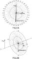
- Figs. 2A and 2C illustrate polar plots representative of the networks of Figs. 1A and 1B , respectively.
- the signals produced by both networks of Figs. 1A and 1B are also shown on a time plots in Figs. 2B and 2D , respectively.
- the crosstalk produced in the plug is represented by the "Plug" vector with a phase of approximately 90 degrees.
- the signal produced by the orthogonal network of Fig. 1A is represented by the "Compensation" vector with a phase of approximately -90 degrees and the orthogonal "OV" vector with a phase of approximately 0 degrees.
- Figs. 2A and 2C illustrate polar plots representative of the networks of Figs. 1A and 1B , respectively.
- the signals produced by both networks of Figs. 1A and 1B are also shown on a time plots in Figs. 2B and 2D , respectively.
- the crosstalk produced in the plug is represented by the "Plug" vector with a phase of
- the crosstalk produced in the plug is represented by the "Plug” vector (illustrated by the dotted vector in Fig. 2C ) with a phase of approximately 90 degrees
- the signal produced by the orthogonal network of Fig. 1B is represented by the "Crosstalk” vector (illustrated by the solid gray shaded vector in Fig. 2C ) with a phase of approximately 90 degrees
- the orthogonal "OV” vector is rotated approximately 90 degrees counterclockwise from the "Compensation"/"Crosstalk” vector of the orthogonal network.
- Fig. 3A illustrates another example of an orthogonal network.
- This network may be referred to as a type 2 orthogonal network and may be implemented inside of a communication jack (e.g., on a PCB) by way of discrete elements, distributed couplings, or any combinations thereof.
- the network of Fig. 3A is illustrated with reference to the 1:2 and 3:6 conductor pairs and achieves the desired compensation between said pairs through inductive and capacitive couplings.
- the desired compensation between the pair 1:2 and pair 3:6 is achieved through the inductive (MOCN 31-3A ) and capacitive (C 31-3A ) couplings between conductor 3 and an offshoot trace OCN1 3A of conductor 1, and the inductive (MOCN 62-3A ) and capacitive (C 62-3A ) couplings between conductor 6 and an offshoot trace OCN2 3A of conductor 2.
- the orthogonal network is enabled with a capacitive coupling C 12-3A (e.g., a discrete capacitor) positioned between the offshoot traces OCN1 3A and OCN2 3A .
- the net resultant signal produced by this network would typically be considered a compensation signal.
- Fig. 3B illustrates how the orthogonal network of Fig. 3A can be implemented to provide a net resultant crosstalk signal.
- the desired coupling between pair 1:2 and pair 3:6 is achieved through the inductive (MOCN 61-3B ) and capacitive (C 61-3B ) couplings between conductor 6 and an offshoot trace OCN1 3B of conductor 1, and the inductive (MOCN 32-3B ) and capacitive (C 32-3B ) couplings between conductor 3 and an offshoot trace OCN2 3B of conductor 2.
- the orthogonal network is enabled with a capacitive coupling C 12-3B (e.g., a discrete capacitor) positioned between the offshoot traces of OCN1 3B and OCN2 3B .
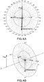
- Figs. 4A and 4C illustrate polar plots representative of the networks of Figs. 3A and 3B , respectively.
- the signals produced by both networks of Figs. 3A and 3B are also shown on a time plots in Figs. 4B and 4D , respectively.
- the crosstalk produced in the plug is represented by the "Plug” vector with a phase of approximately 90 degrees
- the signal produced by the orthogonal network of Fig. 3A is represented by the "Compensation" vector with a phase of approximately -90 degrees and the orthogonal "OV" vector with a phase of approximately 180 degrees.
- Figs. 4A and 4C illustrate polar plots representative of the networks of Figs. 3A and 3B , respectively.
- the signals produced by both networks of Figs. 3A and 3B are also shown on a time plots in Figs. 4B and 4D , respectively.
- the crosstalk produced in the plug is represented by the "Plug" vector with a phase of approximately 90
- the crosstalk produced in the plug is represented by the "Plug” vector (illustrated by the dotted vector in Fig. 4C ) with a phase of approximately 90 degrees
- the signal produced by the orthogonal network of Fig. 3B is represented by the "Crosstalk” vector (illustrated by the solid gray shaded vector in Fig. 4C ) with a phase of approximately 90 degrees
- the orthogonal vector "OV” is rotated approximately 90 degrees clockwise from the "Compensation"/"Crosstalk” vector of the orthogonal network.
- the -90 degree phase shift of the "OV" vector relative to the "Compensation"/"Crosstalk” vector is a fundamental characteristic of a type 2 orthogonal network.
- the different behavior of the networks can be attributed to the direction of the current through Z S on a driving conductor relative to the direction of the current through Z S on a corresponding victim conductor and the underlying layouts of the offshoot traces which permit the current to couple between the corresponding driving and victim conductors. If the direction of the resulting current through Z S on the victim conductor is opposite of the direction of the current through Z S on the driving conductor, then the network may be considered to be a type 1 orthogonal network and the "OV" vector can be expected to have a +90 degree phase shift relative to the "Compensation"/"Crosstalk" vector.
- the network may be considered to be a type 2 orthogonal network and the "OV" vector can be expected to have a -90 degree phase shift relative to the "Compensation"/"Crosstalk" vector.
- the type 1 orthogonal network shown in Fig. 1A if conductor 6 is considered to be the driving conductor, due to the nature of inductive coupling MOCN 62-1A and the layout of the offshoot trace OCN2 1A , the current through Z S in the corresponding victim conductor 2 will have an opposite direction of the current through Z S in conductor 6.
- Each of the orthogonal networks shown in Figs. 1A , 1B , 3A , and 3B shows two signal conductors coupling to two offshoot traces, causing coupling to occur between all four signal conductors of the two differential pairs.
- an orthogonal network implemented between two differential pairs can also be realized by having only one conductor couple to one offshoot trace. Two examples of such single-sided orthogonal networks are shown in Figs. 5 and 6 .
- Fig. 5 illustrates a single-sided type 1 orthogonal network in accordance with one example.
- the network of Fig. 5 may be implemented inside of a communication jack (e.g., on a PCB) by way of discrete elements, distributed couplings, or any combinations thereof.
- the network of Fig. 5 is illustrated with reference to the 1:2 and 3:6 conductor pairs and achieves the desired compensation between said pairs through inductive and capacitive couplings.
- the desired compensation between pair 1:2 and pair 3:6 is achieved through the inductive (MOCN 62-5 ) and capacitive (C 62-5 ) couplings between conductor 6 and an offshoot trace OCN2 5 of conductor 2.
- the orthogonal network is enabled with a capacitive coupling C 12-5 (e.g., a discrete capacitor) positioned between the offshoot trace OCN2 5 and conductor 1.
- C 12-5 e.g., a discrete capacitor
- a single-sided type 1 orthogonal network can be arranged such that the inductive and capacitive couplings occur between certain conductors to produce a net resultant crosstalk signal.
- the network can be arranged so that the inductive (MOCN 62-5 ) and capacitive (C 62-5 ) couplings occur between conductor 3 and the offshoot trace OCN2 5 , with a capacitive coupling C 12-5 remaining between the offshoot trace OCN2 5 and conductor 1.
- Such a configuration would yield a net resultant signal that is generally considered to be a crosstalk signal.
- the implementation of the single-sided orthogonal network of Fig. 5 on conductors 6 and 2 is non-limiting, and other embodiments of a single-sided orthogonal network may be implemented on any desired conductor combination (e.g., conductors 3 and 1).
- Fig. 6 illustrates a single-sided type 2 orthogonal network in accordance with an example.
- the network of Fig. 6 may be implemented inside of a communication jack (e.g., on a PCB) by way of discrete elements, distributed couplings, or any combinations thereof.
- the network of Fig. 6 is shown with reference to the 1:2 and 3:6 conductor pairs and achieves the desired coupling between said pairs through inductive and capacitive couplings.
- the desired coupling between pair 1:2 and pair 3:6 is achieved through the inductive (MOCN 61-6 ) and capacitive (C 61-6 ) couplings between conductor 6 and an offshoot trace OCN1 6 of conductor 1.
- the orthogonal network is enabled with a capacitive coupling C 12-6 (e.g., a discrete capacitor) positioned between the offshoot trace OCN1 6 and conductor 2.
- C 12-6 e.g., a discrete capacitor
- the net resultant signal produced by this network would typically be considered a crosstalk signal.
- a single-sided type 2 orthogonal network can be arranged such that the inductive and capacitive couplings occur between certain conductors to produce a net resultant compensation signal (e.g., the inductive (MOCN 61-6 ) and capacitive (C 61-6 ) couplings occur between conductor 3 and the offshoot trace OCN1 6 , with a capacitive coupling C 12-6 remaining between the offshoot trace OCN1 6 and conductor 2).
- the implementation of the single-sided orthogonal network of Fig. 6 on conductors 6 and 1 is non-limiting, and other embodiments of a single-sided orthogonal network may be implemented on any desired conductor combination (e.g., conductors 3 and 2).
- the vectors representing the couplings of the orthogonal networks change in magnitude depending on the frequency of the signal transmitted across the conductors.
- the magnitude of the vector representing the non-shunting capacitive coupling e.g., the "Compensation" vector in Fig. 2A
- the rate of change of the magnitude of the vector representing the inductive coupling in combination with the shunt capacitive coupling e.g., the "OV" vector in Fig. 2A
- the desired ratio of the vectors' magnitudes may be difficult to attain.
- the "Compensation" vector may grow too fast in relation to the "OV” vector (or conversely, the "OV” vector may grow too slow in relation to the "Compensation” vector) to realize a desired result.
- hybrid orthogonal networks can be implemented inside of a communication jack (e.g., on a PCB) by way of discrete elements, distributed couplings, or any combinations thereof.
- a communication jack e.g., on a PCB
- FIGs. 7A and 7B show a generalized representation of this hybrid network
- Fig. 7B shows a more detailed schematic view thereof.
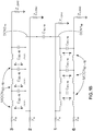
- This network is comprised of four networks, Network 1A, Network 2A, Network 1B, and Network 2B, which may be referred to as sub-networks and may themselves comprise type 1, type 2, or hybrid orthogonal networks.
- Network 1A is a type 1 orthogonal network which provides inductive (MOCN 31-7 ) and capacitive (C 31-7 ) couplings between an offshoot trace OCN1 7 of conductor 1 and conductor 3.
- Network 2A is a type 2 orthogonal network which provides inductive (MOCN 61-7 ) and capacitive (C 61-7 ) couplings between the offshoot trace OCN1 7 and conductor 6.
- Network 1B is a type 1 orthogonal network which provides inductive (MOCN 62-7 ) and capacitive (C 62-7 ) couplings between an offshoot trace OCN2 7 of conductor 2 and conductor 6.
- Network 2B is a type 2 orthogonal network which provides inductive (MOCN 32-7 ) and capacitive (C 32-7 ) couplings between the offshoot trace OCN2 7 and conductor 3.
- Networks 1A and 1B couple conductors 1 and 3, and 2 and 6, respectively, and thus could be said to produce a compensation signal.
- Networks 2A and 2B couple conductors 1 and 6, and 2 and 3, respectively, and thus could be said to produce a crosstalk signal. All the networks are enabled with a capacitive coupling C 12-7 (e.g., a discrete capacitor) positioned between the offshoot traces OCN1 7 and OCN2 7 .
- C 12-7 e.g., a discrete capacitor
- Fig. 8 shows a polar plot representative of the circuit in Fig. 7B .
- the crosstalk produced in the plug is represented by the "Plug” vector with a phase of approximately 90 degrees.
- the "Compensation" vector is the sum of the compensation signals produced by the Networks 1A and 1B and the crosstalk signals produced by the Networks 2A and 2B.
- the net capacitive couplings in Networks 1A and 1B are larger than the net capacitive couplings in Networks 2A and 2B, the net effect will be a compensating vector with a phase of approximately -90 degrees, as shown in Fig. 8 .
- the orthogonal "OV" vector is the sum of the orthogonal vectors produced by Networks 1A, 1B, 2A, and 2B. Given that all the orthogonal vectors produced by the circuit of Fig. 7B have a phase of approximately 0 degrees, the resulting summation vector "OV" also has a phase of approximately 0 degrees as shown in Fig. 8 .
- Fig. 9 illustrates another embodiment of a hybrid orthogonal network.
- This embodiment shows the implementation of type 1 and type 2 orthogonal networks occurring concurrently in the same location to produce a net resultant vector within a single stage.
- the orthogonal networks which produced the compensation and crosstalk signals and coupled to a single conductor i.e., Networks 1A and 2B which coupled to conductor 3, or Networks 2A and 1B which coupled to conductor 6) occurred serially
- the embodiment of Fig. 9 allows both the compensation and crosstalk producing orthogonal networks to couple to a conductor (in this case conductor 6) concurrently.
- the use of the term "concurrently" or the like herein is not necessarily mean to be absolute, but can instead mean a lack of a time delay that is significant enough to appreciably affect the analysis of a circuit.
- the hybrid orthogonal network of Fig. 9 is illustrated with reference to the 1:2 and 3:6 conductor pairs and achieves a desired coupling by using concurrent type 1 and type 2 orthogonal networks.
- the type 1 orthogonal network is comprised of the inductive (MOCN 62-9 ) and capacitive (C 62-9 ) couplings occurring between the offshoot trace OCN2 9 of conductor 2 and conductor 6. Since this network provides coupling between conductors 2 and 6, when enabled, it produces a signal that would typically be considered a compensation signal.
- the type 2 orthogonal network is comprised of the inductive (MOCN 61-9 ) and capacitive (C 61-9 ) couplings between the offshoot trace OCN1 9 of conductor 1 and conductor 6.
- this network provides coupling between conductors 1 and 6, when enabled, it produces a signal that would typically be considered a crosstalk signal.
- the entire hybrid network is enabled with a capacitive coupling C 12-9 (e.g., a discrete capacitor) positioned between the offshoot traces OCN1 9 and OCN2 9 .
- Fig. 10A shows a polar plot representative of the hybrid orthogonal network of Fig. 9 .
- the crosstalk produced in the plug is represented by the "Plug” vector with a phase of approximately 90 degrees.
- the signal of the type 1 orthogonal network is represented by the "Compensation” vector with a phase of approximately -90 degrees and the “OV COMP " vector (illustrated by the solid gray shaded vector) with a phase of approximately 0 degrees.
- the "Compensation” vector is the result of the C 62-9 capacitive coupling and the "OV COMP " vector is the result of the MOCN 62-9 inductive coupling in combination with the C 12-9 capacitive coupling.
- the signal of the type 2 orthogonal network is represented by the "Crosstalk” vector with a phase of approximately 90 degrees and the "OV XTALK " vector (illustrated by the dotted vector) with a phase of approximately 0 degrees.
- the "Crosstalk” vector is the result of the C 61-9 capacitive coupling and the “OV XTALK” vector is the result of the MOCN 61-9 inductive coupling in combination with the C 12-9 capacitive coupling.
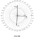
- the polar plot of Fig. 10A can be simplified to show the net resultant vectors by summing the "Crosstalk” and “Compensation” vectors to produce the "A1" vector, and the "OV XTALK “ and “OV COMP " vectors to produce the "B1" vector, resulting in the polar plot of Fig. 10B .
- hybrid orthogonal network As a result of using a hybrid orthogonal network, one may be able to achieve a wide range of ratios between the "A1" and "B1" vectors within a single stage. Such versatility may permit the use of hybrid orthogonal networks in an array of applications, including providing necessary compensation within a communication jack to achieve Category 6 (CAT6), Category 6a (CAT6a), or greater performance.
- CAT6 Category 6
- CAT6a Category 6a
- FIG. 11 shows a typical application of an exemplary jack which may employ one or more compensation network(s) in accordance with various embodiments of the present invention.
- This figure illustrates an electrical system 10 having a patch panel 12 with at least one jack 20 mounted therein and connected to a data cable (not shown).
- a plug 14, connected to a cable 16, can mate with the jack(s) 20 which allows data to flow in both directions through these components.
- jack 20 includes a front housing 22, a front sled 24 with plug interface contacts (PICs) 25, a PCB 26, insulation displacement contacts (IDCs) 28, a rear sled 30, and a wire cap 32.
- PICs plug interface contacts
- IDCs insulation displacement contacts
- jack 20 includes a front housing 22, a front sled 24 with plug interface contacts (PICs) 25, a PCB 26, insulation displacement contacts (IDCs) 28, a rear sled 30, and a wire cap 32.
- PICs plug interface contacts
- IDCs insulation displacement contacts
- PCB 26 An exemplary embodiment of PCB 26, which includes multiple embodiments of orthogonal networks thereon, is shown in Figs. 13-16 .
- Fig. 13 illustrates the individual layers of PCB 26.
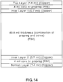
- PCB 26 can use the stack-up shown in Fig. 14 .
- PCB 26 can have a 4-layer construction, with capacitors being formed by the top layer and inner layer 1, and the bottom layer and inner layer 2. This may be achieved by using a 4-mil core or prepreg (partially cured FR4 without copper cladding, for example) at the top and bottom of PCB 26 and standard circuit board assembly materials within the rest of the circuit board.
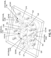
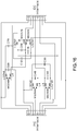
- An isometric view of PCB 26 is shown in Fig. 15 , and a corresponding schematic is shown in Fig. 16 . Note that other PCB constructions (e.g., 2-layer, 6-layer, etc.) can be used.
- FIG. 16 illustrates inductors and capacitors as discrete elements
- at least some of these elements represent the capacitive and inductive coupling occurring between various electrical traces.
- Such coupling is generally distributed and may, for example, include: (a) distributed coupling occurring as a result of two traces running within proximity to each other; (b) coupling occurring as a result of discrete elements such as, but not limited to, pad capacitors, finger capacitors, or other discrete capacitors; or (c) a combination thereof.
- PCB 26 includes signal traces S1, S2, S3, S4, S5, S6, S7, and S8.
- Each of the S1-S8 traces respectively correspond to the 1 st -8 th plug contacts of a plug having its contacts laid out in accordance with ANSI/TIA-568-C.2, and electronically connect the respective PICs 25 to the respective IDCs 28.
- These signal traces generate self-inductances with self-inductances L4, L5, and L6 being shown on the respective S4, S5, and S6 signal traces in Fig. 16 .
- PCB 26 includes offshoot traces to connect (directly or indirectly) PIC conductors 1 and 2 to capacitor C12, PIC conductors 3 and 6 to capacitor C36, and PIC conductors 7 and 8 to capacitor C78.
- the offshoot traces may span more than a single layer of the PCB 26.
- capacitors C12, C36, and C78 may be realized by way of distributed capacitive coupling; discrete elements, including, but not limited to, pad capacitors and finger capacitors; or any combination of distributed capacitive coupling and discrete elements.
- capacitors C12, C36, and C78 may be referred to as "shunt capacitors," as they couple two conductors of the same signal pair.
- At least some of the offshoot traces comprise traces OCN1, OCN2, OCN3, OCN6, and OCN8, which create self-inductances LOCN1, LOCN2, LOCN3, LOCN6, and LOCN8, respectively.
- MOCN16 in PCB 26 is the mutual inductive coupling between S6 (L6) and OCN1 (LOCN1); MOCN26 in PCB 26 is the mutual inductive coupling between S6 (L6) and OCN2 (LOCN2); MOCN46 in PCB 26 is the mutual inductive coupling between S4 (L4) and OCN6 (LOCN6); MOCN35 in PCB 26 is the mutual inductive coupling between S5 (L5) and OCN3 (LOCN3); and MOCN68 in PCB 26 is the mutual inductive coupling between S6 (L6) and OCN8 (LOCN8).
- C16 in PCB 26 is the capacitive coupling between traces S6 and OCN1;
- C26 in PCB 26 is the capacitive coupling between traces S6 and OCN2;
- C46 in PCB 26 is the capacitive coupling between traces S4 and OCN6;
- C35 in PCB 26 is the capacitive coupling between traces S5 and OCN3;
- C68 in PCB 26 is the capacitive coupling between traces S6 and OCN8.
- the compensation network located on the PCB 26 is a type 1 orthogonal network which uses traces S4, S5, OCN3, and OCN6, and capacitor C36 to create the desired signal.
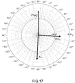
- Fig. 17 illustrates the resulting couplings on a representative polar plot. Traces S4 and OCN6 create the capacitive coupling C46, and traces S5 and OCN3 create the capacitive coupling C35.
- Each capacitive coupling C46 and C35 is approximately 0.6 pF (picofarads) (+/-20%), and together produce a net compensation vector "A 1 " of an opposite polarity of the plug crosstalk vector "Plug.”
- Capacitor C36 (approximately 1.8 pF +/-20%) provides a current path between traces OCN3 and OCN6, allowing mutual inductive coupling MOCN46 to occur between traces S4 and OCN6, and mutual inductive coupling MOCN35 to occur between traces S5 and OCN3.
- Each inductive coupling MOCN46 and MOCN35 is approximately 5 nH (nanohenry) +/-20%.
- both of the inductive couplings MOCN46 and MOCN35 produce a net orthogonal vector "OV 1 .”
- the inductive couplings MOCN46 and MOCN35 are created by the same PCB artwork, and thus occur in generally the same physical locations, as capacitive couplings C46 and C35, respectively.
- the net resultant vector of couplings C35, C46, MOCN35, MOCN46, and C36 provides additional NEXT bandwidth which may help to allow wire-pair combination 4:5-3:6 to meet standards for Category 6 and beyond.
- the orthogonal network located on the PCB 26 uses traces S6, OCN1, and OCN2, and capacitor C12 to create the desired signal.
- This network employs a combination of type 1 and type 2 orthogonal networks resulting in a hybrid orthogonal network.
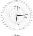
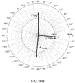
- Figs 18A and 18B illustrate the resulting couplings on a representative polar plot with Fig. 18A showing vectors for the individual type 1 and type 2 networks and Fig. 18B showing a net resultant signal of the hybrid network.
- the type 1 orthogonal network is comprised of the capacitive and inductive couplings occurring between traces S6 and OCN2
- the type 2 orthogonal network is comprised of the capacitive and inductive couplings occurring between traces S6 and OCN1.
- traces S6 and OCN2 create the capacitive coupling C26 (approximately 0.70 pF +/-20%) which produces a compensation vector "A 26 " of an opposite polarity of the plug crosstalk vector "Plug.”
- Traces S6 and OCN1 create capacitive coupling C16 (approximately 0.54 pF +/-20%) which produces a crosstalk vector "A 16 " of the same polarity as the plug crosstalk vector "Plug.”
- the summation of the "A 16 " and “A 26 " vectors produces a net resultant vector "A 16+26 " (see Fig.
- Capacitor C12 (approximately 1.3 pF +/-20%) provides a current path between traces OCN1 and OCN2, allowing mutual inductive coupling MOCN16 to occur between traces S6 and OCN1, and mutual inductive coupling MOCN26 to occur between traces S6 and OCN2.
- Each inductive coupling MOCN16 and MOCN26 is approximately 1.85 nH +/-20%.
- the inductive couplings MOCN16 and MOCN26 are created by the same PCB artwork, and thus occur in generally the same physical locations, as capacitive couplings C16 and C26, respectively. Furthermore, the time delay between the type 1 orthogonal network producing the MOCN26 and C26 couplings and the type 2 orthogonal network producing the MOCN16 and C16 couplings is approximately zero. In other words, while there may be a relatively small time delay due to the lengths of the offshoot traces, this delay is insignificant for the purposes of the analysis of this circuit, and coupling along both of the type 1 and type 2 networks can be said to occur concurrently.
- Such a configuration may allow the compensation network on the 3:6-1:2 wire-pair combination to produce a more desirable range of ratios between the signals represented by the net "A 16+26 " vector and the net “OV 16+26 " vector.
- the net resultant vector of couplings C16, C26, MOCN16, MOCN26, and C12 provides additional NEXT bandwidth which may help to allow wire-pair combination 3:6-1:2 to meet standards for Category 6 and beyond.
- the compensation network located on the PCB 26 is a type 1 orthogonal network which uses traces S6 and OCN8, and capacitor C78 to create the desired signal.
- Fig. 19 illustrates the resulting couplings on a representative polar plot.
- Capacitor C78 (approximately 1.3 pF +/-20%) provides a current path between traces OCN8 and S7, allowing mutual inductive coupling MOCN68 (approximately 1.4 nH +/-20%) to occur between traces S6 and OCN8.
- the inductive coupling MOCN68 is created by the same PCB artwork, and thus occurs in generally the same physical location, as capacitive coupling C68.
- the inductive coupling MOCN68 produces a vector "OV 68 " that is orthogonal to the vector "A 68 " produced by the C68 capacitive coupling.
- the net resultant vector of couplings C68, MOCN68, and C78 provides additional NEXT bandwidth which may help to allow wire-pair combination 3:6-7:8 to meet standards for Category 6 and beyond.
- Table 1 Relationship of PCB 26 Circuit Elements, and "A” and “OV” Vectors: Pair Combination "A” Vector “OV” Vector Capacitor Mutual Inductive Coupling 4:5-3:6 C35, C46 C36 MOCN35, MOCN46 3:6-1:2 C16, C26 C12 MOCN16, MOCN26 3:6-7:8 C68 C78 MOCN68 4:5-1:2 N/A N/A N/A 4:5-7:8 N/A N/A N/A 1:2-7:8 N/A N/A N/A N/A N/A
- the orthogonal network(s) described herein may be implemented within a communication plug (e.g., RJ45 plug).
- the positioning of any such orthogonal network may be similar to the previously-described embodiments in that the plug can include plug contacts instead of the jack PICs, cable connector contacts, and circuitry connecting the plug contacts to respective cable connector contacts, where the orthogonal network(s) may be implemented on said circuitry.
- Orthogonal networks of such embodiments may be used to generate some particular levels of crosstalk.
Landscapes
- Engineering & Computer Science (AREA)
- Microelectronics & Electronic Packaging (AREA)
- Computer Networks & Wireless Communication (AREA)
- Signal Processing (AREA)
- Physics & Mathematics (AREA)
- Electromagnetism (AREA)
- Power Engineering (AREA)
- Details Of Connecting Devices For Male And Female Coupling (AREA)
- Cable Transmission Systems, Equalization Of Radio And Reduction Of Echo (AREA)
Description
- The present invention generally relates to the field of network communication, and more specifically to networks for crosstalk reduction/compensation and communication connectors which employ such networks.
- The evolution of computing has witnessed a significant shift in the importance of networks. An ever-increasing quantity of information is constantly being gathered, stored, and shared among a wide range of users. In addition to the sheer growth of data, users have come to expect quicker access to this information. This combination of size and speed has created a need for network infrastructure capable of supporting a high data rate.
- Current networks readily employ jacks and plugs, and other communication connectors. These connectors typically include closely spaced parallel conductors which allow the jack and the plug to interface to each other. Conventional communication connectors have been used in relatively low data rate applications with relatively few problems. However, as transmission frequency and data rates increase, crosstalk (particularly near-end crosstalk (NEXT)) due to capacitive and inductive couplings among the closely spaced parallel conductors within the jack and/or plug has become increasingly problematic.
- Therefore, it is desirable to have communication connectors capable of achieving improved performance.
- Document
US 7850492 B1 discloses a communication jack that has a housing with a face having a plug receiving aperture. - Document
US 2009/298344 A1 discloses a connector system for the transmission of high-frequency signals, in particular on twisted-pair lines. - Accordingly, embodiments of the present invention are directed to communication connectors and/or internal components thereof.
- In one embodiment, the present invention is a communication connector that includes the features of
claim 1. - In another embodiment, the present invention is a communication system that includes communication equipment and a communication connector according to
claim 1. - In yet another embodiment, the present invention is a method of compensating for noise in a communication connector that includes a plurality of signal pairs. The method includes the steps of claim 9.
- An example is a communication connector that includes plug interface contacts, cable connector contacts, and circuitry connecting the plug interface contacts to respective the cable connector contacts. The circuitry includes signal conductors between respective the plug interface contacts and respective the cable connector contacts, the signal conductors include a first signal pair and a second signal pair, the circuitry includes a network with a first combined mutually inductive and capacitive coupling between a first conductor of the first signal pair and a first conductor of the second signal pair, the network further includes a second combined mutually inductive and capacitive coupling between a second conductor of the first signal pair and the first conductor of the second signal pair, and a shunt capacitive coupling connecting the first conductor of the first signal pair and the second conductor of the first signal pair. In a variation of this embodiment, this communication connector is used in a communication system.
- Another example is a method of compensating for noise in a communication connector including a first signal pair and a second signal pair, the method includes the steps of: (1) reactively crosstalk coupling a first conductor of the first signal pair and a first conductor of the second signal pair, the crosstalk coupling having a first orthogonal component; (2) reactively compensation coupling a second conductor of the first signal pair and the first conductor of the second signal pair, the compensation coupling having a second orthogonal component; and (3) controlling a magnitude of an orthogonal vector representing a combination of the first and second orthogonal components by adjusting the crosstalk coupling and the compensation coupling.
- These and other features, aspects, and advantages of the present invention will become better-understood with reference to the following drawings, description, and any claims that may follow.
-
-
Fig. 1A illustrates atype 1 orthogonal network producing a net compensation signal according to an example. -
Fig. 1B illustrates atype 1 orthogonal network producing a net crosstalk signal according to an example. -
Fig. 2A illustrates a polar plot representative of the orthogonal network ofFig. 1A . -
Fig. 2B illustrates signals shown in the polar plot ofFig. 2A on a time scale. -
Fig. 2C illustrates a polar plot representative of the orthogonal network ofFig. 1B . -
Fig. 2D illustrates signals shown in the polar plot ofFig. 2C on a time scale. -
Fig. 3A illustrates atype 2 orthogonal network producing a net compensation signal according to an example. -
Fig. 3B illustrates atype 2 orthogonal network producing a net crosstalk signal according to an example. -
Fig. 4A illustrates a polar plot representative of the orthogonal network ofFig. 3A . -
Fig. 4B illustrates signals shown in the polar plot ofFig. 4A on a time scale. -
Fig. 4C illustrates a polar plot representative of the orthogonal network ofFig. 3B . -
Fig. 4D illustrates signals shown in the polar plot ofFig. 4C on a time scale. -
Fig. 5 illustrates atype 1 orthogonal network producing a net compensation signal according to an example. -
Fig. 6 illustrates atype 2 orthogonal network producing a net crosstalk signal according to an example. -
Fig. 7A illustrates a block diagram of a hybrid orthogonal network according to an embodiment of the present invention. -
Fig. 7B illustrates an exemplary schematic of the orthogonal network ofFig. 7A . -
Fig. 8 illustrates a polar plot representative of the orthogonal network ofFig. 7B . -
Fig. 9 illustrates a hybrid orthogonal network according to another embodiment of the present invention. -
Figs. 10A and10B illustrate polar plots representative of the orthogonal network ofFig. 9 . -
Fig. 11 illustrates a perspective view of a portion of a communication system according to an embodiment of the present invention. -
Fig. 12 illustrates an exploded view of a communication jack used in the communication system ofFig. 11 , according to an embodiment of the present invention. -
Fig. 13 illustrates top views of four conductive layers of a printed circuit board of the jack ofFig. 12 according to an embodiment of the present invention. -
Fig. 14 illustrates a printed circuit board stack-up according to an embodiment of the present invention. -
Fig. 15 illustrates an isometric view of the assembled printed circuit board ofFigs. 13 and14 . -
Fig. 16 illustrates a schematic view of the printed circuit board ofFig. 15 . -
Fig. 17 illustrates a polar plot representative of the orthogonal network on the 3:6-4:5 wire pair of the printed circuit board ofFig. 15 . -
Figs. 18A and18B illustrate polar plots representative of the orthogonal network on the 1:2-3:6 wire pair of the printed circuit board ofFig. 15 . -
Fig. 19 illustrates a polar plot representative of the orthogonal network on the 3:6-7:8 wire pair of the printed circuit board ofFig. 15 . - As used herein, "opposite polarity" can be defined as being approximately 180 degrees out of phase in relation to a referenced polarity, and "orthogonal" can be defined as being approximately 90 degrees out of phase in relation to a referenced polarity. Also, as used herein, references to "shunting" can be defined as direct or indirect coupling of two conductors of the same differential pair via some means. For example, a shunting capacitive coupling on a wire pair (e.g., 3:6 wire pair) can refer to some form of a capacitive coupling (e.g., pad capacitor) positioned between a first conductor (e.g., conductor 3) and second conductor (e.g., conductor 6) of that wire pair. Note that indirect coupling may include intervening components such as offshoot traces. Conversely, "non-shunting" can be defined as direct or indirect coupling of two conductors of different differential pairs via some means. Furthermore, "conductor(s)," "signal conductor(s)," and "signal trace(s)" may be used interchangeably and shall be understood to refer to the same feature.
- In RJ45 plug/jack connector combinations, NEXT generally occurs between the neighboring conductors of differential pairs. For example, in an RJ45 plug/jack connector combination which has the plug conductors laid out in accordance with ANSI/TIA-568-C.2, NEXT can exist between conductor pairs 1:2 and 3:6, conductor pairs 3:6 and 4:5, and conductor pairs 3:6 and 7:8. In case of conductor pairs 1:2 and 3:6, NEXT can occur due to the coupling which can primarily exist between
conductors conductors conductors conductors - The following exemplary embodiments illustrate how the present invention attempts to reduce or otherwise compensate for the crosstalk which may appear between differential pairs of a communication plug/jack combination. The present invention may rely in part on the principles of crosstalk compensation disclosed in
U.S. Patent Application Serial No.: 13/681,480, filed on November 20, 2012 -
Fig. 1A illustrates an example of an orthogonal network. This network may be referred to as atype 1 orthogonal network, and may be implemented inside of a communication jack (e.g., on a printed circuit board (PCB)) by way of discrete elements, distributed couplings, or any combinations thereof. The network ofFig. 1 is illustrated with reference to the 1:2 and 3:6 conductor pairs and achieves the desired compensation between said pairs through inductive and capacitive couplings. In particular, the desired coupling between pair 1:2 and pair 3:6 is achieved through the inductive (MOCN31-1A) and capacitive (C31-1A) couplings betweenconductor 3 and an offshoot trace OCN11A ofconductor 1, and the inductive (MOCN62-1A) and capacitive (C62-1A) couplings betweenconductor 6 and an offshoot trace OCN21A ofconductor 2. The orthogonal network is enabled with a capacitive coupling C12-1A (e.g., a discrete capacitor) positioned between the offshoot traces OCN11A and OCN21A. The net resultant signal produced by this network would typically be considered a compensation signal. -
Fig. 1B illustrates how the orthogonal network ofFig. 1A can be implemented to provide a net resultant crosstalk signal. As explained further in the specification, such a crosstalk signal may be beneficial in attaining a desired level of overall compensation within a communication jack. The desired coupling between pair 1:2 and pair 3:6 is achieved through the inductive (MOCN32-1B) and capacitive (C32-1B) couplings betweenconductor 3 and an offshoot trace OCN21B ofconductor 2, and the inductive (MOCN61-1B) and capacitive (C61-1B) couplings betweenconductor 6 and an offshoot trace OCN11B ofconductor 1. The orthogonal network is enabled with a capacitive coupling C12-1B (e.g., a discrete capacitor) positioned between the offshoot traces OCN11B and OCN21B. -
Figs. 2A and2C illustrate polar plots representative of the networks ofFigs. 1A and1B , respectively. The signals produced by both networks ofFigs. 1A and1B are also shown on a time plots inFigs. 2B and2D , respectively. With respect toFigs. 2A and 2B , the crosstalk produced in the plug is represented by the "Plug" vector with a phase of approximately 90 degrees. The signal produced by the orthogonal network ofFig. 1A is represented by the "Compensation" vector with a phase of approximately -90 degrees and the orthogonal "OV" vector with a phase of approximately 0 degrees. With respect toFigs. 2C and 2D , the crosstalk produced in the plug is represented by the "Plug" vector (illustrated by the dotted vector inFig. 2C ) with a phase of approximately 90 degrees, and the signal produced by the orthogonal network ofFig. 1B is represented by the "Crosstalk" vector (illustrated by the solid gray shaded vector inFig. 2C ) with a phase of approximately 90 degrees and the orthogonal "OV" vector with a phase of approximately 180 degrees. In both cases, the orthogonal vector "OV" is rotated approximately 90 degrees counterclockwise from the "Compensation"/"Crosstalk" vector of the orthogonal network. The +90 degree phase shift of the "OV" vector relative to the "Compensation"/"Crosstalk" vector as disclosed inU.S. Patent Application Serial No.: 13/681,480 (previously mentioned) is a characteristic of atype 1 orthogonal network. -
Fig. 3A illustrates another example of an orthogonal network. This network may be referred to as atype 2 orthogonal network and may be implemented inside of a communication jack (e.g., on a PCB) by way of discrete elements, distributed couplings, or any combinations thereof. The network ofFig. 3A is illustrated with reference to the 1:2 and 3:6 conductor pairs and achieves the desired compensation between said pairs through inductive and capacitive couplings. In particular, the desired compensation between the pair 1:2 and pair 3:6 is achieved through the inductive (MOCN31-3A) and capacitive (C31-3A) couplings betweenconductor 3 and an offshoot trace OCN13A ofconductor 1, and the inductive (MOCN62-3A) and capacitive (C62-3A) couplings betweenconductor 6 and an offshoot trace OCN23A ofconductor 2. The orthogonal network is enabled with a capacitive coupling C12-3A (e.g., a discrete capacitor) positioned between the offshoot traces OCN13A and OCN23A. The net resultant signal produced by this network would typically be considered a compensation signal. -
Fig. 3B illustrates how the orthogonal network ofFig. 3A can be implemented to provide a net resultant crosstalk signal. The desired coupling between pair 1:2 and pair 3:6 is achieved through the inductive (MOCN61-3B) and capacitive (C61-3B) couplings betweenconductor 6 and an offshoot trace OCN13B ofconductor 1, and the inductive (MOCN32-3B) and capacitive (C32-3B) couplings betweenconductor 3 and an offshoot trace OCN23B ofconductor 2. The orthogonal network is enabled with a capacitive coupling C12-3B (e.g., a discrete capacitor) positioned between the offshoot traces of OCN13B and OCN23B. -
Figs. 4A and4C illustrate polar plots representative of the networks ofFigs. 3A and3B , respectively. The signals produced by both networks ofFigs. 3A and3B are also shown on a time plots inFigs. 4B and4D , respectively. With respect toFigs. 4A and 4B , the crosstalk produced in the plug is represented by the "Plug" vector with a phase of approximately 90 degrees, and the signal produced by the orthogonal network ofFig. 3A is represented by the "Compensation" vector with a phase of approximately -90 degrees and the orthogonal "OV" vector with a phase of approximately 180 degrees. With respect toFigs. 4C and 4D , the crosstalk produced in the plug is represented by the "Plug" vector (illustrated by the dotted vector inFig. 4C ) with a phase of approximately 90 degrees, and the signal produced by the orthogonal network ofFig. 3B is represented by the "Crosstalk" vector (illustrated by the solid gray shaded vector inFig. 4C ) with a phase of approximately 90 degrees and the orthogonal "OV" vector with a phase of approximately 0 degrees. In both cases, the orthogonal vector "OV" is rotated approximately 90 degrees clockwise from the "Compensation"/"Crosstalk" vector of the orthogonal network. The -90 degree phase shift of the "OV" vector relative to the "Compensation"/"Crosstalk" vector is a fundamental characteristic of atype 2 orthogonal network. - When the polar plots of a
type 1 orthogonal network are compared to the polar plots of atype 2 orthogonal network, one will notice that the orthogonal positioning (clockwise vs. counterclockwise rotation) of the "OV" vector relative to the "Compensation"/"Crosstalk" vector is different for both types of networks. Whereas atype 1 orthogonal network produces an "OV" vector which is rotated approximately 90 degrees counterclockwise from the "Compensation"/"Crosstalk" vector, atype 2 orthogonal network produces an "OV" vector which is rotated approximately 90 degrees clockwise from the "Compensation"/"Crosstalk" vector. The different behavior of the networks can be attributed to the direction of the current through ZS on a driving conductor relative to the direction of the current through ZS on a corresponding victim conductor and the underlying layouts of the offshoot traces which permit the current to couple between the corresponding driving and victim conductors. If the direction of the resulting current through ZS on the victim conductor is opposite of the direction of the current through ZS on the driving conductor, then the network may be considered to be atype 1 orthogonal network and the "OV" vector can be expected to have a +90 degree phase shift relative to the "Compensation"/"Crosstalk" vector. If, however, the direction of the resulting current through ZS on the victim conductor is the same as the direction of the current through ZS on the driving conductor, then the network may be considered to be atype 2 orthogonal network and the "OV" vector can be expected to have a -90 degree phase shift relative to the "Compensation"/"Crosstalk" vector. For example, in thetype 1 orthogonal network shown inFig. 1A , ifconductor 6 is considered to be the driving conductor, due to the nature of inductive coupling MOCN62-1A and the layout of the offshoot trace OCN21A, the current through ZS in thecorresponding victim conductor 2 will have an opposite direction of the current through ZS inconductor 6. On the other hand, in thetype 2 orthogonal network shown inFig. 3A , ifconductor 6 is considered to be the source signal driving conductor, due to the nature of inductive coupling MOCN62-3A and the layout of the offshoot trace OCN23A, the current through ZS in thecorresponding victim conductor 2 will have the same direction as the current through ZS inconductor 6. - Each of the orthogonal networks shown in
Figs. 1A ,1B ,3A , and3B shows two signal conductors coupling to two offshoot traces, causing coupling to occur between all four signal conductors of the two differential pairs. However, an orthogonal network implemented between two differential pairs can also be realized by having only one conductor couple to one offshoot trace. Two examples of such single-sided orthogonal networks are shown inFigs. 5 and6 . -
Fig. 5 illustrates a single-sided type 1 orthogonal network in accordance with one example. Like the other networks described herein, the network ofFig. 5 may be implemented inside of a communication jack (e.g., on a PCB) by way of discrete elements, distributed couplings, or any combinations thereof. - The network of
Fig. 5 is illustrated with reference to the 1:2 and 3:6 conductor pairs and achieves the desired compensation between said pairs through inductive and capacitive couplings. In particular, the desired compensation between pair 1:2 and pair 3:6 is achieved through the inductive (MOCN62-5) and capacitive (C62-5) couplings betweenconductor 6 and an offshoot trace OCN25 ofconductor 2. The orthogonal network is enabled with a capacitive coupling C12-5 (e.g., a discrete capacitor) positioned between the offshoot trace OCN25 andconductor 1. The net resultant signal produced by this network would typically be considered a compensation signal. However, it should be understood that a single-sided type 1 orthogonal network can be arranged such that the inductive and capacitive couplings occur between certain conductors to produce a net resultant crosstalk signal. For example, the network can be arranged so that the inductive (MOCN62-5) and capacitive (C62-5) couplings occur betweenconductor 3 and the offshoot trace OCN25, with a capacitive coupling C12-5 remaining between the offshoot trace OCN25 andconductor 1. Such a configuration would yield a net resultant signal that is generally considered to be a crosstalk signal. It should be further understood that the implementation of the single-sided orthogonal network ofFig. 5 onconductors conductors 3 and 1). -
Fig. 6 illustrates a single-sided type 2 orthogonal network in accordance with an example. Like the other networks described herein, the network ofFig. 6 may be implemented inside of a communication jack (e.g., on a PCB) by way of discrete elements, distributed couplings, or any combinations thereof. The network ofFig. 6 is shown with reference to the 1:2 and 3:6 conductor pairs and achieves the desired coupling between said pairs through inductive and capacitive couplings. In particular, the desired coupling between pair 1:2 and pair 3:6 is achieved through the inductive (MOCN61-6) and capacitive (C61-6) couplings betweenconductor 6 and an offshoot trace OCN16 ofconductor 1. The orthogonal network is enabled with a capacitive coupling C12-6 (e.g., a discrete capacitor) positioned between the offshoot trace OCN16 andconductor 2. The net resultant signal produced by this network would typically be considered a crosstalk signal. However, similar to the single-sided type 1 orthogonal network, it should be understood that a single-sided type 2 orthogonal network can be arranged such that the inductive and capacitive couplings occur between certain conductors to produce a net resultant compensation signal (e.g., the inductive (MOCN61-6) and capacitive (C61-6) couplings occur betweenconductor 3 and the offshoot trace OCN16, with a capacitive coupling C12-6 remaining between the offshoot trace OCN16 and conductor 2). Likewise, it should be further understood that the implementation of the single-sided orthogonal network ofFig. 6 onconductors conductors 3 and 2). - As discussed in some detail in the
U.S. Patent Application Serial No.: 13/681,480 , the vectors representing the couplings of the orthogonal networks change in magnitude depending on the frequency of the signal transmitted across the conductors. Furthermore, in some embodiments the magnitude of the vector representing the non-shunting capacitive coupling (e.g., the "Compensation" vector inFig. 2A ) changes at a rate that is different than the rate of change of the magnitude of the vector representing the inductive coupling in combination with the shunt capacitive coupling (e.g., the "OV" vector inFig. 2A ). As a result, in some instances, the desired ratio of the vectors' magnitudes may be difficult to attain. For example, the "Compensation" vector may grow too fast in relation to the "OV" vector (or conversely, the "OV" vector may grow too slow in relation to the "Compensation" vector) to realize a desired result. In such instances, it may be possible to achieve a desired result by varying and/or combining thetype 1 andtype 2 orthogonal networks to produce expanded or otherwise hybrid orthogonal networks. - Similar to the previous embodiments, hybrid orthogonal networks can be implemented inside of a communication jack (e.g., on a PCB) by way of discrete elements, distributed couplings, or any combinations thereof. One exemplary embodiment of such a hybrid orthogonal network is illustrated in
Figs. 7A and7B with reference to the 1:2 and 3:6 conductor pairs.Fig. 7A shows a generalized representation of this hybrid network andFig. 7B shows a more detailed schematic view thereof. This network is comprised of four networks,Network 1A,Network 2A,Network 1B, andNetwork 2B, which may be referred to as sub-networks and may themselves comprisetype 1,type 2, or hybrid orthogonal networks.Network 1A is atype 1 orthogonal network which provides inductive (MOCN31-7) and capacitive (C31-7) couplings between an offshoot trace OCN17 ofconductor 1 andconductor 3.Network 2A is atype 2 orthogonal network which provides inductive (MOCN61-7) and capacitive (C61-7) couplings between the offshoot trace OCN17 andconductor 6.Network 1B is atype 1 orthogonal network which provides inductive (MOCN62-7) and capacitive (C62-7) couplings between an offshoot trace OCN27 ofconductor 2 andconductor 6. AndNetwork 2B is atype 2 orthogonal network which provides inductive (MOCN32-7) and capacitive (C32-7) couplings between the offshoot trace OCN27 andconductor 3.Networks 1B couple conductors Networks 2B couple conductors -
Fig. 8 shows a polar plot representative of the circuit inFig. 7B . The crosstalk produced in the plug is represented by the "Plug" vector with a phase of approximately 90 degrees. The "Compensation" vector is the sum of the compensation signals produced by theNetworks Networks Networks Networks Fig. 8 . However, if the net capacitive couplings inNetworks Networks Networks Fig. 7B have a phase of approximately 0 degrees, the resulting summation vector "OV" also has a phase of approximately 0 degrees as shown inFig. 8 . -
Fig. 9 illustrates another embodiment of a hybrid orthogonal network. This embodiment shows the implementation oftype 1 andtype 2 orthogonal networks occurring concurrently in the same location to produce a net resultant vector within a single stage. In other words, whereas in the embodiment described inFigs. 7A and7B the orthogonal networks which produced the compensation and crosstalk signals and coupled to a single conductor (i.e.,Networks conductor 3, orNetworks Fig. 9 allows both the compensation and crosstalk producing orthogonal networks to couple to a conductor (in this case conductor 6) concurrently. Note that the use of the term "concurrently" or the like herein is not necessarily mean to be absolute, but can instead mean a lack of a time delay that is significant enough to appreciably affect the analysis of a circuit. - The hybrid orthogonal network of
Fig. 9 is illustrated with reference to the 1:2 and 3:6 conductor pairs and achieves a desired coupling by usingconcurrent type 1 andtype 2 orthogonal networks. Thetype 1 orthogonal network is comprised of the inductive (MOCN62-9) and capacitive (C62-9) couplings occurring between the offshoot trace OCN29 ofconductor 2 andconductor 6. Since this network provides coupling betweenconductors type 2 orthogonal network is comprised of the inductive (MOCN61-9) and capacitive (C61-9) couplings between the offshoot trace OCN19 ofconductor 1 andconductor 6. Since this network provides coupling betweenconductors -
Fig. 10A shows a polar plot representative of the hybrid orthogonal network ofFig. 9 . The crosstalk produced in the plug is represented by the "Plug" vector with a phase of approximately 90 degrees. The signal of thetype 1 orthogonal network is represented by the "Compensation" vector with a phase of approximately -90 degrees and the "OVCOMP" vector (illustrated by the solid gray shaded vector) with a phase of approximately 0 degrees. The "Compensation" vector is the result of the C62-9 capacitive coupling and the "OVCOMP" vector is the result of the MOCN62-9 inductive coupling in combination with the C12-9 capacitive coupling. The signal of thetype 2 orthogonal network is represented by the "Crosstalk" vector with a phase of approximately 90 degrees and the "OVXTALK" vector (illustrated by the dotted vector) with a phase of approximately 0 degrees. The "Crosstalk" vector is the result of the C61-9 capacitive coupling and the "OVXTALK" vector is the result of the MOCN61-9 inductive coupling in combination with the C12-9 capacitive coupling. - The polar plot of
Fig. 10A can be simplified to show the net resultant vectors by summing the "Crosstalk" and "Compensation" vectors to produce the "A1" vector, and the "OVXTALK" and "OVCOMP" vectors to produce the "B1" vector, resulting in the polar plot ofFig. 10B . Note that by providingconcurrent type 1 andtype 2 orthogonal networks, either of which may produce compensation or crosstalk coupling, one may be able to better manage the relationship between the net non-shunting capacitive coupling (which in the case the orthogonal network ofFig. 9 produces the net "A1" vector) and the net inductive coupling combined with the shunting capacitive coupling (which in the case the orthogonal network ofFig. 9 produces the net "B1" vector). Also note that the magnitudes of the "Compensation" and "Crosstalk" vectors can be varied within the hybrid network ofFig. 9 (by adjusting the amount of coupling) to produce a net resultant vector "A1" that provides either a net crosstalk or a net compensation signal. For example, if the magnitude of the "Crosstalk" vector was greater than the magnitude of the "Compensation" vector, the net resultant vector would provide a net crosstalk signal. The hybrid orthogonal network ofFig. 9 can also be modified, in accordance with the present specification, to adjust the directionality of either of the "OV" vectors to obtain a specifically desired net resultant "B1" vector. - As a result of using a hybrid orthogonal network, one may be able to achieve a wide range of ratios between the "A1" and "B1" vectors within a single stage. Such versatility may permit the use of hybrid orthogonal networks in an array of applications, including providing necessary compensation within a communication jack to achieve Category 6 (CAT6), Category 6a (CAT6a), or greater performance.
-
Fig. 11 shows a typical application of an exemplary jack which may employ one or more compensation network(s) in accordance with various embodiments of the present invention. This figure illustrates anelectrical system 10 having apatch panel 12 with at least onejack 20 mounted therein and connected to a data cable (not shown). Aplug 14, connected to acable 16, can mate with the jack(s) 20 which allows data to flow in both directions through these components. - As shown in
Fig. 12 , in one exemplary embodiment,jack 20 includes afront housing 22, afront sled 24 with plug interface contacts (PICs) 25, aPCB 26, insulation displacement contacts (IDCs) 28, arear sled 30, and awire cap 32. Other elements, and details ofjack 20 can be found inU.S. Patent No. 7,052,328 (Ciezak et al. ), entitled "Electronic Connector And Method Of Performing Electronic Connection," issued on 05/30/2006;U.S. Patent No. 7,481,681 (Caveney et al. ), entitled "Electrical Connector With Improved Crosstalk Compensation," issued on 01/27/2009;U.S. Patent No. 7,452,245 (Doorhy et al. ), entitled "Wire Containment Cap," issued on 11/18/2008; andU.S. Patent No. 7,476,120 (Patel et al. ), entitled "Wire Containment Cap With Integral Strain Relief Clip," issued on 01/13/2009. - An exemplary embodiment of
PCB 26, which includes multiple embodiments of orthogonal networks thereon, is shown inFigs. 13-16 .Fig. 13 illustrates the individual layers ofPCB 26. In this embodiment,PCB 26 can use the stack-up shown inFig. 14 .PCB 26 can have a 4-layer construction, with capacitors being formed by the top layer andinner layer 1, and the bottom layer andinner layer 2. This may be achieved by using a 4-mil core or prepreg (partially cured FR4 without copper cladding, for example) at the top and bottom ofPCB 26 and standard circuit board assembly materials within the rest of the circuit board. An isometric view ofPCB 26 is shown inFig. 15 , and a corresponding schematic is shown inFig. 16 . Note that other PCB constructions (e.g., 2-layer, 6-layer, etc.) can be used. - While the schematic of
Fig. 16 illustrates inductors and capacitors as discrete elements, in at least one embodiment, at least some of these elements represent the capacitive and inductive coupling occurring between various electrical traces. Such coupling is generally distributed and may, for example, include: (a) distributed coupling occurring as a result of two traces running within proximity to each other; (b) coupling occurring as a result of discrete elements such as, but not limited to, pad capacitors, finger capacitors, or other discrete capacitors; or (c) a combination thereof. -
PCB 26 includes signal traces S1, S2, S3, S4, S5, S6, S7, and S8. Each of the S1-S8 traces respectively correspond to the 1st-8th plug contacts of a plug having its contacts laid out in accordance with ANSI/TIA-568-C.2, and electronically connect therespective PICs 25 to therespective IDCs 28. These signal traces generate self-inductances with self-inductances L4, L5, and L6 being shown on the respective S4, S5, and S6 signal traces inFig. 16 . Additionally,PCB 26 includes offshoot traces to connect (directly or indirectly)PIC conductors PIC conductors PIC conductors PCB 26. In alternate embodiments, capacitors C12, C36, and C78 may be realized by way of distributed capacitive coupling; discrete elements, including, but not limited to, pad capacitors and finger capacitors; or any combination of distributed capacitive coupling and discrete elements. Additionally, capacitors C12, C36, and C78 may be referred to as "shunt capacitors," as they couple two conductors of the same signal pair. At least some of the offshoot traces comprise traces OCN1, OCN2, OCN3, OCN6, and OCN8, which create self-inductances LOCN1, LOCN2, LOCN3, LOCN6, and LOCN8, respectively. - The result of the signal S traces being within a proximity to the OCN traces is mutual inductive coupling between the respective S and OCN traces. In particular, MOCN16 in
PCB 26 is the mutual inductive coupling between S6 (L6) and OCN1 (LOCN1); MOCN26 inPCB 26 is the mutual inductive coupling between S6 (L6) and OCN2 (LOCN2); MOCN46 inPCB 26 is the mutual inductive coupling between S4 (L4) and OCN6 (LOCN6); MOCN35 inPCB 26 is the mutual inductive coupling between S5 (L5) and OCN3 (LOCN3); and MOCN68 inPCB 26 is the mutual inductive coupling between S6 (L6) and OCN8 (LOCN8). Another result of the S traces being within a proximity to the OCN traces is capacitive coupling between the respective S and OCN traces. In particular, C16 inPCB 26 is the capacitive coupling between traces S6 and OCN1; C26 inPCB 26 is the capacitive coupling between traces S6 and OCN2; C46 inPCB 26 is the capacitive coupling between traces S4 and OCN6; C35 inPCB 26 is the capacitive coupling between traces S5 and OCN3; and C68 inPCB 26 is the capacitive coupling between traces S6 and OCN8. - For wire-pair combination 4:5-3:6, the compensation network located on the
PCB 26 is atype 1 orthogonal network which uses traces S4, S5, OCN3, and OCN6, and capacitor C36 to create the desired signal.Fig. 17 illustrates the resulting couplings on a representative polar plot. Traces S4 and OCN6 create the capacitive coupling C46, and traces S5 and OCN3 create the capacitive coupling C35. Each capacitive coupling C46 and C35 is approximately 0.6 pF (picofarads) (+/-20%), and together produce a net compensation vector "A1" of an opposite polarity of the plug crosstalk vector "Plug." Capacitor C36 (approximately 1.8 pF +/-20%) provides a current path between traces OCN3 and OCN6, allowing mutual inductive coupling MOCN46 to occur between traces S4 and OCN6, and mutual inductive coupling MOCN35 to occur between traces S5 and OCN3. Each inductive coupling MOCN46 and MOCN35 is approximately 5 nH (nanohenry) +/-20%. Together, and in combination with the C36 capacitor, both of the inductive couplings MOCN46 and MOCN35 produce a net orthogonal vector "OV1." The inductive couplings MOCN46 and MOCN35 are created by the same PCB artwork, and thus occur in generally the same physical locations, as capacitive couplings C46 and C35, respectively. The net resultant vector of couplings C35, C46, MOCN35, MOCN46, and C36 provides additional NEXT bandwidth which may help to allow wire-pair combination 4:5-3:6 to meet standards forCategory 6 and beyond. - For wire-pair combination 3:6-1:2, the orthogonal network located on the
PCB 26 uses traces S6, OCN1, and OCN2, and capacitor C12 to create the desired signal. This network employs a combination oftype 1 andtype 2 orthogonal networks resulting in a hybrid orthogonal network.Figs 18A and18B illustrate the resulting couplings on a representative polar plot withFig. 18A showing vectors for theindividual type 1 andtype 2 networks andFig. 18B showing a net resultant signal of the hybrid network. In this hybrid network, thetype 1 orthogonal network is comprised of the capacitive and inductive couplings occurring between traces S6 and OCN2, and thetype 2 orthogonal network is comprised of the capacitive and inductive couplings occurring between traces S6 and OCN1. - In particular, traces S6 and OCN2 create the capacitive coupling C26 (approximately 0.70 pF +/-20%) which produces a compensation vector "A26" of an opposite polarity of the plug crosstalk vector "Plug." Traces S6 and OCN1 create capacitive coupling C16 (approximately 0.54 pF +/-20%) which produces a crosstalk vector "A16" of the same polarity as the plug crosstalk vector "Plug." The summation of the "A16" and "A26" vectors produces a net resultant vector "A16+26" (see
Fig. 18B ) having an opposite polarity of the plug crosstalk vector "Plug." Capacitor C12 (approximately 1.3 pF +/-20%) provides a current path between traces OCN1 and OCN2, allowing mutual inductive coupling MOCN16 to occur between traces S6 and OCN1, and mutual inductive coupling MOCN26 to occur between traces S6 and OCN2. Each inductive coupling MOCN16 and MOCN26 is approximately 1.85 nH +/-20%. Since the mutual inductive coupling MOCN16 occurs in atype 2 orthogonal network, its signal (in combination with the shunt capacitor C12), represented by the "OV16" vector (illustrated by the dotted vector) inFig 18A , has a phase shift of approximately -90 degrees relative to the signal produced by the capacitive coupling C16 (represented by the "A16" vector) of that same network. On the other hand, since the mutual inductive coupling MOCN26 occurs in atype 1 orthogonal network, its signal (in combination with the shunt capacitor C12), represented by the "OV26" vector (illustrated by the solid gray shaded vector), has a phase shift of approximately 90 degrees relative to the signal produced by the capacitive coupling C26 (represented by vector "A26") of that same network. The summation of the "OV16" and "OV26" vectors produces a net resultant vector "OV16+26" which is approximately orthogonal to the "A16+26" vector. - The inductive couplings MOCN16 and MOCN26 are created by the same PCB artwork, and thus occur in generally the same physical locations, as capacitive couplings C16 and C26, respectively. Furthermore, the time delay between the
type 1 orthogonal network producing the MOCN26 and C26 couplings and thetype 2 orthogonal network producing the MOCN16 and C16 couplings is approximately zero. In other words, while there may be a relatively small time delay due to the lengths of the offshoot traces, this delay is insignificant for the purposes of the analysis of this circuit, and coupling along both of thetype 1 andtype 2 networks can be said to occur concurrently. Such a configuration may allow the compensation network on the 3:6-1:2 wire-pair combination to produce a more desirable range of ratios between the signals represented by the net "A16+26" vector and the net "OV16+26" vector. The net resultant vector of couplings C16, C26, MOCN16, MOCN26, and C12 provides additional NEXT bandwidth which may help to allow wire-pair combination 3:6-1:2 to meet standards forCategory 6 and beyond. - For wire-pair combination 3:6-7:8, the compensation network located on the
PCB 26 is atype 1 orthogonal network which uses traces S6 and OCN8, and capacitor C78 to create the desired signal.Fig. 19 illustrates the resulting couplings on a representative polar plot. Traces S6 and OCN8 create capacitive coupling C68 (approximately 0.5 pF +/-20%) which produces a compensation vector "A68" of an opposite polarity of the plug crosstalk vector "Plug." Capacitor C78 (approximately 1.3 pF +/-20%) provides a current path between traces OCN8 and S7, allowing mutual inductive coupling MOCN68 (approximately 1.4 nH +/-20%) to occur between traces S6 and OCN8. The inductive coupling MOCN68 is created by the same PCB artwork, and thus occurs in generally the same physical location, as capacitive coupling C68. In combination with the C78 capacitor, the inductive coupling MOCN68 produces a vector "OV68" that is orthogonal to the vector "A68" produced by the C68 capacitive coupling. The net resultant vector of couplings C68, MOCN68, and C78 provides additional NEXT bandwidth which may help to allow wire-pair combination 3:6-7:8 to meet standards forCategory 6 and beyond. - A summary of the circuit elements of
PCB 26 and how they generally relate to the described vectors is given in Table 1 below.Table 1 Relationship of PCB 26 Circuit Elements, and "A" and "OV" Vectors:Pair Combination "A" Vector "OV" Vector Capacitor Mutual Inductive Coupling 4:5-3:6 C35, C46 C36 MOCN35, MOCN46 3:6-1:2 C16, C26 C12 MOCN16, MOCN26 3:6-7:8 C68 C78 MOCN68 4:5-1:2 N/A N/A N/A 4:5-7:8 N/A N/A N/A 1:2-7:8 N/A N/A N/A - In other embodiments of the invention, the orthogonal network(s) described herein may be implemented within a communication plug (e.g., RJ45 plug). The positioning of any such orthogonal network may be similar to the previously-described embodiments in that the plug can include plug contacts instead of the jack PICs, cable connector contacts, and circuitry connecting the plug contacts to respective cable connector contacts, where the orthogonal network(s) may be implemented on said circuitry. Orthogonal networks of such embodiments may be used to generate some particular levels of crosstalk.
Claims (10)
- A communication connector (20), comprising:plug interface contacts (25);cable connector contacts (28); anda circuitry connecting said plug interface contacts to respective said cable connector contacts, said circuitry including signal conductors (1, 2, 3, 6) between respective said plug interface contacts and respective said cable connector contacts, said signal conductors including a first signal pair (1, 2) and a second signal pair (6, 3), said circuitry including a network with a first combined mutually inductive (MOCN6-19) and capacitive (C61-9) coupling between a first conductor (1) of said first signal pair (1, 2) and a first conductor (6) of said second signal pair (6, 3), said network further including a second combined mutually inductive (MOCN62-9) and capacitive (C62-9) coupling between a second conductor (2) of said first signal pair (1,2) and said first conductor (6) of said second signal pair (6, 3), and a shunt capacitive coupling (C12-9) connecting said first conductor (1) of said first signal pair (1, 2) and said second conductor (2) of said first signal pair (1, 2), wherein said circuitry further includes a first offshoot trace (OCN19) connecting said first conductor (1) of said first signal pair (1, 2) and said shunt capacitive coupling (C12-9), a second offshoot trace (OCN29) connecting said second conductor (2) of said first signal pair and said shunt capacitive coupling, characterised in that said first combined mutually inductive and capacitive coupling occurs via said first offshoot trace, and said second combined mutually inductive and capacitive coupling occurs via said second offshoot trace.
- The communication connector of claim 1, wherein said first combined mutually inductive and capacitive coupling (MOCN61-9, C61-9) and said second combined mutually inductive and capacitive coupling (MOCN62-9, C62-9) occur concurrently.
- The communication connector of claim 1, wherein said communication connector is a communication plug.
- The communication connector of claim 1, wherein said communication connector is an RJ45 jack.
- The communication connector of claim 1, wherein said circuitry is implemented on a printed circuit board.
- The communication connector of claim 1, wherein at least one of said first combined coupling (MOCN61-9, C61-9), said second combined coupling (MOCN62-9, C62-9), and said shunt capacitive coupling (C12-9) is formed by at least one of a discrete element, distributed coupling, and a combination thereof.
- A communication system, comprising:communication equipment;and a communication connector according to any of claims 1, 2, 4, 5, 6.
- A method of compensating for noise in a communication connector, comprising:plug interface contacts (25);cable connector contacts (28); anda circuitry connecting said plug interface contacts to respective said cable connector contacts, said circuitry including signal conductors (1, 2, 3, 6) between respective said plug interface contacts and respective said cable connector contacts, said signal conductors including a first signal pair (1, 2) and a second signal pair (6, 3), said method comprising the steps of:reactively crosstalk coupling a first conductor (1) of said first signal pair and a first conductor of said second signal pair (6) by a network with a first combined mutually inductive (MOCN6-19) and capacitive (C61-9) coupling, said crosstalk coupling having a first orthogonal component;reactively compensation coupling a second conductor of said first signal pair and said first conductor of said second signal pair by the network that further includes a second combined mutually inductive (MOCN62-9) and capacitive (C61-9) coupling, said compensation coupling having a second orthogonal component;connecting said first conductor (1) of said first signal pair (1,2) and said second conductor (2) of said first signal pair (1,2) by a shunt capacitive coupling (C12-9) andcontrolling a magnitude of an orthogonal vector representing a combination of said first and second orthogonal components by adjusting said crosstalk coupling and said compensation coupling;wherein said communication connector (20) further includes a first offshoot trace (OCN19) connected to said first conductor (1) of said first signal pair (1, 2) and a second offshoot trace (OCN29) connected to said second conductor (2) of said first signal pair (1, 2),wherein said step of reactively crosstalk coupling said first conductor (1) of said first signal pair (1, 2) and said first conductor (1) of said second signal pair (6,3) includes coupling said first conductor (6) of said second signal pair (6, 3) and said first offshoot trace (OCN19), andwherein said step of reactively compensation coupling said second conductor (2) of said first signal pair (1, 2) and said first conductor (6) of said second signal pair (6,3) includes coupling said first conductor (6) of said second signal pair (6,3) and said second offshoot trace (OCN29),wherein said first and second orthogonal components are turned on by positioning a shunt capacitive coupling (C12-9) between said first (OCN19) and second (OCN29) offshoot traces;wherein at least one of said reactively crosstalk coupling and reactively compensation coupling is achieved by providing a discrete element, distributed coupling, and a combination thereof.
- The method of claim 8 wherein said communication connector is an RJ45 jack.
- The method of claim 8, wherein said step of reactively crosstalk coupling and said step of reactively compensation coupling occur concurrently.
Applications Claiming Priority (3)
| Application Number | Priority Date | Filing Date | Title |
|---|---|---|---|
| US201361774225P | 2013-03-07 | 2013-03-07 | |
| US14/198,291 US9246463B2 (en) | 2013-03-07 | 2014-03-05 | Compensation networks and communication connectors using said compensation networks |
| PCT/US2014/021030 WO2014138342A1 (en) | 2013-03-07 | 2014-03-06 | Compensation networks and communication connectors using said compensation networks |
Publications (2)
| Publication Number | Publication Date |
|---|---|
| EP2965595A1 EP2965595A1 (en) | 2016-01-13 |
| EP2965595B1 true EP2965595B1 (en) | 2020-06-24 |
Family
ID=51488348
Family Applications (1)
| Application Number | Title | Priority Date | Filing Date |
|---|---|---|---|
| EP14711433.4A Active EP2965595B1 (en) | 2013-03-07 | 2014-03-06 | Communication connector, communication system and method for compensating noise in same |
Country Status (4)
| Country | Link |
|---|---|
| US (1) | US9246463B2 (en) |
| EP (1) | EP2965595B1 (en) |
| JP (1) | JP6109350B2 (en) |
| WO (1) | WO2014138342A1 (en) |
Families Citing this family (3)
| Publication number | Priority date | Publication date | Assignee | Title |
|---|---|---|---|---|
| US9257792B2 (en) * | 2013-03-14 | 2016-02-09 | Panduit Corp. | Connectors and systems having improved crosstalk performance |
| CN106341097B (en) * | 2015-07-06 | 2019-06-18 | 创意电子股份有限公司 | Common mode filter and circuit structure |
| WO2018081712A1 (en) | 2016-10-31 | 2018-05-03 | Commscope Technologies Llc | Connector with capacitive crosstalk compensation |
Citations (8)
| Publication number | Priority date | Publication date | Assignee | Title |
|---|---|---|---|---|
| US6089923A (en) * | 1999-08-20 | 2000-07-18 | Adc Telecommunications, Inc. | Jack including crosstalk compensation for printed circuit board |
| WO2004047240A2 (en) * | 2002-11-20 | 2004-06-03 | The Siemon Company | Apparatus for crosstalk compensation in a telecommunications connector |
| US20080268710A1 (en) * | 2004-05-14 | 2008-10-30 | Amid Hashim | Next High Frequency Improvement by Using Frequency Dependent Effective Capacitance |
| US20090298344A1 (en) * | 2008-06-03 | 2009-12-03 | Mc Technology Gmbh | Connector system |
| WO2010019785A1 (en) * | 2008-08-13 | 2010-02-18 | Panduit Corp. | Communications connector with multi-stage compensation |
| US20100048040A1 (en) * | 2008-08-20 | 2010-02-25 | Panduit Corp. | High-speed connector with multi-stage compensation |
| US20100190357A1 (en) * | 2009-01-26 | 2010-07-29 | Amid Hashim | Printed Wiring Boards and Communication Connectors Having Series Inductor-Capacitor Crosstalk Compensation Circuits that Share a Common Inductor |
| US7850492B1 (en) * | 2009-11-03 | 2010-12-14 | Panduit Corp. | Communication connector with improved crosstalk compensation |
Family Cites Families (88)
| Publication number | Priority date | Publication date | Assignee | Title |
|---|---|---|---|---|
| US5299956B1 (en) | 1992-03-23 | 1995-10-24 | Superior Modular Prod Inc | Low cross talk electrical connector system |
| US5432484A (en) | 1992-08-20 | 1995-07-11 | Hubbell Incorporated | Connector for communication systems with cancelled crosstalk |
| US5295869A (en) | 1992-12-18 | 1994-03-22 | The Siemon Company | Electrically balanced connector assembly |
| US6464529B1 (en) | 1993-03-12 | 2002-10-15 | Cekan/Cdt A/S | Connector element for high-speed data communications |
| US5362257A (en) | 1993-07-08 | 1994-11-08 | The Whitaker Corporation | Communications connector terminal arrays having noise cancelling capabilities |
| JPH07176336A (en) | 1993-09-30 | 1995-07-14 | Siemon Co:The | Electrically expanded wiring block with break test capability |
| US5470244A (en) | 1993-10-05 | 1995-11-28 | Thomas & Betts Corporation | Electrical connector having reduced cross-talk |
| GB2271678B (en) | 1993-12-03 | 1994-10-12 | Itt Ind Ltd | Electrical connector |
| EP0692884B1 (en) | 1994-07-14 | 2002-03-20 | Molex Incorporated | Modular connector with reduced crosstalk |
| US5586914A (en) | 1995-05-19 | 1996-12-24 | The Whitaker Corporation | Electrical connector and an associated method for compensating for crosstalk between a plurality of conductors |
| US5791943A (en) | 1995-11-22 | 1998-08-11 | The Siemon Company | Reduced crosstalk modular outlet |
| US5700167A (en) | 1996-09-06 | 1997-12-23 | Lucent Technologies | Connector cross-talk compensation |
| US5938479A (en) | 1997-04-02 | 1999-08-17 | Communications Systems, Inc. | Connector for reducing electromagnetic field coupling |
| US5997358A (en) | 1997-09-02 | 1999-12-07 | Lucent Technologies Inc. | Electrical connector having time-delayed signal compensation |
| CH693012A5 (en) | 1997-06-02 | 2003-01-15 | Reichle & De Massari Fa | A plug connector for high-frequency data transmission over electrical conductors. |
| KR100287956B1 (en) | 1997-12-26 | 2001-09-17 | 이 은 신 | Differential mode crosstalk suppression apparatus for unshielded twisted pair |
| EP1072069A4 (en) | 1998-04-16 | 2002-01-09 | Thomas & Betts Int | Crosstalk reducing electrical jack and plug connector |
| US6526807B1 (en) * | 1998-06-18 | 2003-03-04 | Joseph Doumit | Early warning water leak detection system |
| US6356162B1 (en) | 1999-04-02 | 2002-03-12 | Nordx/Cdt, Inc. | Impedance compensation for a cable and connector |
| US6168474B1 (en) | 1999-06-04 | 2001-01-02 | Lucent Technologies Inc. | Communications connector having crosstalk compensation |
| US6186834B1 (en) | 1999-06-08 | 2001-02-13 | Avaya Technology Corp. | Enhanced communication connector assembly with crosstalk compensation |
| US6176742B1 (en) | 1999-06-25 | 2001-01-23 | Avaya Inc. | Capacitive crosstalk compensation arrangement for communication connectors |
| US6196880B1 (en) | 1999-09-21 | 2001-03-06 | Avaya Technology Corp. | Communication connector assembly with crosstalk compensation |
| EP1128491B1 (en) | 2000-02-21 | 2004-09-15 | Reichle & De-Massari AG | Electrical connection member |
| US6379198B1 (en) | 2000-03-13 | 2002-04-30 | Avaya Technology Corp. | Electrical connector terminal construction |
| US6283795B1 (en) | 2000-03-14 | 2001-09-04 | Surtec Industries Inc. | Electrical connector with reduced attenuation, near-end cross talk, and return loss |
| US6533618B1 (en) | 2000-03-31 | 2003-03-18 | Ortronics, Inc. | Bi-directional balance low noise communication interface |
| US6270381B1 (en) | 2000-07-07 | 2001-08-07 | Avaya Technology Corp. | Crosstalk compensation for electrical connectors |
| US6379157B1 (en) | 2000-08-18 | 2002-04-30 | Leviton Manufacturing Co., Inc. | Communication connector with inductive compensation |
| US6435918B1 (en) | 2000-09-18 | 2002-08-20 | Surtec Industries Inc. | Reduced return loss electrical connector |
| US6464541B1 (en) | 2001-05-23 | 2002-10-15 | Avaya Technology Corp. | Simultaneous near-end and far-end crosstalk compensation in a communication connector |
| US6866548B2 (en) | 2002-10-23 | 2005-03-15 | Avaya Technology Corp. | Correcting for near-end crosstalk unbalance caused by deployment of crosstalk compensation on other pairs |
| US6964587B2 (en) | 2002-11-10 | 2005-11-15 | Bel Fuse Ltd. | High performance, high capacitance gain, jack connector for data transmission or the like |
| US7052328B2 (en) | 2002-11-27 | 2006-05-30 | Panduit Corp. | Electronic connector and method of performing electronic connection |
| US7176383B2 (en) | 2003-12-22 | 2007-02-13 | Endicott Interconnect Technologies, Inc. | Printed circuit board with low cross-talk noise |
| US7265300B2 (en) | 2003-03-21 | 2007-09-04 | Commscope Solutions Properties, Llc | Next high frequency improvement using hybrid substrates of two materials with different dielectric constant frequency slopes |
| EP1695419A4 (en) | 2003-11-21 | 2008-02-20 | Leviton Manufacturing Co | WIRING PANEL WITH CROSSTALK REDUCTION SYSTEM AND METHOD THEREOF |
| US7182649B2 (en) | 2003-12-22 | 2007-02-27 | Panduit Corp. | Inductive and capacitive coupling balancing electrical connector |
| US6916209B1 (en) | 2004-01-23 | 2005-07-12 | Molex Incorporated | Electrical signal transmission system |
| US7179131B2 (en) | 2004-02-12 | 2007-02-20 | Panduit Corp. | Methods and apparatus for reducing crosstalk in electrical connectors |
| WO2005084341A2 (en) | 2004-03-03 | 2005-09-15 | Hubbell Incorporated | Midspan patch panel with circuit separation for data terminal equipment, power insertion and data collection |
| US20050195583A1 (en) | 2004-03-03 | 2005-09-08 | Hubbell Incorporated. | Midspan patch panel with circuit separation for data terminal equipment, power insertion and data collection |
| CN102082367B (en) | 2004-03-12 | 2013-11-20 | 泛达公司 | Methods and apparatus for reducing crosstalk in electrical connectors |
| US7153168B2 (en) | 2004-04-06 | 2006-12-26 | Panduit Corp. | Electrical connector with improved crosstalk compensation |
| US7980900B2 (en) | 2004-05-14 | 2011-07-19 | Commscope, Inc. Of North Carolina | Next high frequency improvement by using frequency dependent effective capacitance |
| US7038554B2 (en) | 2004-05-17 | 2006-05-02 | Leviton Manufacturing Co., Inc. | Crosstalk compensation with balancing capacitance system and method |
| US7281957B2 (en) | 2004-07-13 | 2007-10-16 | Panduit Corp. | Communications connector with flexible printed circuit board |
| US7452245B2 (en) | 2004-08-04 | 2008-11-18 | Panduit Corp. | Wire containment cap |
| US7168993B2 (en) | 2004-12-06 | 2007-01-30 | Commscope Solutions Properties Llc | Communications connector with floating wiring board for imparting crosstalk compensation between conductors |
| US7204722B2 (en) | 2004-12-07 | 2007-04-17 | Commscope Solutions Properties, Llc | Communications jack with compensation for differential to differential and differential to common mode crosstalk |
| US7166000B2 (en) | 2004-12-07 | 2007-01-23 | Commscope Solutions Properties, Llc | Communications connector with leadframe contact wires that compensate differential to common mode crosstalk |
| US7320624B2 (en) | 2004-12-16 | 2008-01-22 | Commscope, Inc. Of North Carolina | Communications jacks with compensation for differential to differential and differential to common mode crosstalk |
| CN101080856B (en) | 2004-12-17 | 2011-01-19 | 泛达公司 | Wire Guards with Combined Strain Relief Collets |
| US7175476B2 (en) | 2005-01-11 | 2007-02-13 | Daeun Electronics Co., Ltd. | Crosstalk canceling pattern for high-speed communications and modular jack having the same |
| WO2006081423A1 (en) | 2005-01-28 | 2006-08-03 | Commscope Inc. Of North Carolina | Controlled mode conversion connector for reduced alien crosstalk |
| US7314393B2 (en) | 2005-05-27 | 2008-01-01 | Commscope, Inc. Of North Carolina | Communications connectors with floating wiring board for imparting crosstalk compensation between conductors |
| EP1987569A1 (en) | 2006-02-13 | 2008-11-05 | Panduit Corp. | Connector with crosstalk compensation |
| US7367849B2 (en) | 2006-03-07 | 2008-05-06 | Surtec Industries, Inc. | Electrical connector with shortened contact and crosstalk compensation |
| US7787615B2 (en) | 2006-04-11 | 2010-08-31 | Adc Telecommunications, Inc. | Telecommunications jack with crosstalk compensation and arrangements for reducing return loss |
| US7381098B2 (en) | 2006-04-11 | 2008-06-03 | Adc Telecommunications, Inc. | Telecommunications jack with crosstalk multi-zone crosstalk compensation and method for designing |
| US7402085B2 (en) | 2006-04-11 | 2008-07-22 | Adc Gmbh | Telecommunications jack with crosstalk compensation provided on a multi-layer circuit board |
| US7591686B2 (en) | 2006-04-18 | 2009-09-22 | Commscope, Inc. Of North Carolina | Communications connectors with jackwire contacts and printed circuit boards |
| US7294025B1 (en) | 2006-04-21 | 2007-11-13 | Surtec Industries, Inc. | High performance jack |
| US7686650B2 (en) | 2006-05-17 | 2010-03-30 | Bel Fuse Ltd. | High speed modular jack with flexible compensation circuit |
| US7530854B2 (en) | 2006-06-15 | 2009-05-12 | Ortronics, Inc. | Low noise multiport connector |
| US7364470B2 (en) | 2006-07-05 | 2008-04-29 | Commscope, Inc. Of North Carolina | Communications connectors with signal current splitting |
| ES2541130T3 (en) | 2006-10-13 | 2015-07-16 | Tyco Electronics Services Gmbh | Connection physical support with inductive and capacitive multi-stage crosstalk compensation |
| AU2007201114B2 (en) | 2007-03-14 | 2011-04-07 | Tyco Electronics Services Gmbh | Electrical Connector |
| AU2007201106B9 (en) | 2007-03-14 | 2011-06-02 | Tyco Electronics Services Gmbh | Electrical Connector |
| US7874878B2 (en) | 2007-03-20 | 2011-01-25 | Panduit Corp. | Plug/jack system having PCB with lattice network |
| US7427218B1 (en) | 2007-05-23 | 2008-09-23 | Commscope, Inc. Of North Carolina | Communications connectors with staggered contacts that connect to a printed circuit board via contact pads |
| US7485010B2 (en) | 2007-06-14 | 2009-02-03 | Ortronics, Inc. | Modular connector exhibiting quad reactance balance functionality |
| WO2009039459A2 (en) | 2007-09-19 | 2009-03-26 | Leviton Manufacturing Co., Inc. | Internal crosstalk compensation circuit formed on a flexible printed circuit board positioned within a communications outlet, and methods and systems relating to same |
| US7967645B2 (en) * | 2007-09-19 | 2011-06-28 | Leviton Manufacturing Co., Inc. | High speed data communications connector circuits, systems, and methods for reducing crosstalk in communications systems |
| CA2709965C (en) | 2007-12-19 | 2016-07-19 | Panduit Corp. | Method and system for reducing common mode signal generation within a plug/jack connection |
| US7841909B2 (en) | 2008-02-12 | 2010-11-30 | Adc Gmbh | Multistage capacitive far end crosstalk compensation arrangement |
| US7976348B2 (en) | 2008-05-07 | 2011-07-12 | Ortronics, Inc. | Modular insert and jack including moveable reactance section |
| US7914345B2 (en) | 2008-08-13 | 2011-03-29 | Tyco Electronics Corporation | Electrical connector with improved compensation |
| US7682203B1 (en) | 2008-11-04 | 2010-03-23 | Commscope, Inc. Of North Carolina | Communications jacks having contact wire configurations that provide crosstalk compensation |
| US7914346B2 (en) | 2008-11-04 | 2011-03-29 | Commscope, Inc. Of North Carolina | Communications jacks having contact wire configurations that provide crosstalk compensation |
| US8202128B2 (en) | 2008-11-25 | 2012-06-19 | Adc Gmbh | Telecommunications jack with adjustable crosstalk compensation |
| US8167661B2 (en) | 2008-12-02 | 2012-05-01 | Panduit Corp. | Method and system for improving crosstalk attenuation within a plug/jack connection and between nearby plug/jack combinations |
| US8197286B2 (en) | 2009-06-11 | 2012-06-12 | Commscope, Inc. Of North Carolina | Communications plugs having capacitors that inject offending crosstalk after a plug-jack mating point and related connectors and methods |
| US8016621B2 (en) | 2009-08-25 | 2011-09-13 | Tyco Electronics Corporation | Electrical connector having an electrically parallel compensation region |
| US7909656B1 (en) | 2009-10-26 | 2011-03-22 | Leviton Manufacturing Co., Inc. | High speed data communications connector with reduced modal conversion |
| US8279745B2 (en) | 2009-11-23 | 2012-10-02 | Telefonaktiebolaget L M Ericsson (Publ) | Orthogonal vector DSL |
| US7976349B2 (en) | 2009-12-08 | 2011-07-12 | Commscope, Inc. Of North Carolina | Communications patching and connector systems having multi-stage near-end alien crosstalk compensation circuits |
| US9088116B2 (en) | 2011-11-23 | 2015-07-21 | Panduit Corp. | Compensation network using an orthogonal compensation network |
-
2014
- 2014-03-05 US US14/198,291 patent/US9246463B2/en active Active
- 2014-03-06 JP JP2015561638A patent/JP6109350B2/en active Active
- 2014-03-06 WO PCT/US2014/021030 patent/WO2014138342A1/en not_active Ceased
- 2014-03-06 EP EP14711433.4A patent/EP2965595B1/en active Active
Patent Citations (8)
| Publication number | Priority date | Publication date | Assignee | Title |
|---|---|---|---|---|
| US6089923A (en) * | 1999-08-20 | 2000-07-18 | Adc Telecommunications, Inc. | Jack including crosstalk compensation for printed circuit board |
| WO2004047240A2 (en) * | 2002-11-20 | 2004-06-03 | The Siemon Company | Apparatus for crosstalk compensation in a telecommunications connector |
| US20080268710A1 (en) * | 2004-05-14 | 2008-10-30 | Amid Hashim | Next High Frequency Improvement by Using Frequency Dependent Effective Capacitance |
| US20090298344A1 (en) * | 2008-06-03 | 2009-12-03 | Mc Technology Gmbh | Connector system |
| WO2010019785A1 (en) * | 2008-08-13 | 2010-02-18 | Panduit Corp. | Communications connector with multi-stage compensation |
| US20100048040A1 (en) * | 2008-08-20 | 2010-02-25 | Panduit Corp. | High-speed connector with multi-stage compensation |
| US20100190357A1 (en) * | 2009-01-26 | 2010-07-29 | Amid Hashim | Printed Wiring Boards and Communication Connectors Having Series Inductor-Capacitor Crosstalk Compensation Circuits that Share a Common Inductor |
| US7850492B1 (en) * | 2009-11-03 | 2010-12-14 | Panduit Corp. | Communication connector with improved crosstalk compensation |
Also Published As
| Publication number | Publication date |
|---|---|
| WO2014138342A1 (en) | 2014-09-12 |
| US20140256182A1 (en) | 2014-09-11 |
| EP2965595A1 (en) | 2016-01-13 |
| US9246463B2 (en) | 2016-01-26 |
| JP2016511515A (en) | 2016-04-14 |
| JP6109350B2 (en) | 2017-04-05 |
Similar Documents
| Publication | Publication Date | Title |
|---|---|---|
| US8137141B2 (en) | High-speed connector with multi-stage compensation | |
| US8047879B2 (en) | Printed wiring boards and communication connectors having series inductor-capacitor crosstalk compensation circuits that share a common inductor | |
| US9356396B2 (en) | Communication connector with crosstalk compensation | |
| US7201618B2 (en) | Controlled mode conversion connector for reduced alien crosstalk | |
| US8052474B2 (en) | Plug/jack system having PCB with lattice network | |
| EP2319138B1 (en) | Communications connector with multi-stage compensation | |
| US9246274B2 (en) | Communication connectors having crosstalk compensation networks | |
| US9246463B2 (en) | Compensation networks and communication connectors using said compensation networks | |
| US9640914B2 (en) | Connectors and systems having improved crosstalk performance | |
| HK1151893B (en) | Communications connector with multi-stage compensation |
Legal Events
| Date | Code | Title | Description |
|---|---|---|---|
| PUAI | Public reference made under article 153(3) epc to a published international application that has entered the european phase |
Free format text: ORIGINAL CODE: 0009012 |
|
| 17P | Request for examination filed |
Effective date: 20151007 |
|
| AK | Designated contracting states |
Kind code of ref document: A1 Designated state(s): AL AT BE BG CH CY CZ DE DK EE ES FI FR GB GR HR HU IE IS IT LI LT LU LV MC MK MT NL NO PL PT RO RS SE SI SK SM TR |
|
| AX | Request for extension of the european patent |
Extension state: BA ME |
|
| DAX | Request for extension of the european patent (deleted) | ||
| STAA | Information on the status of an ep patent application or granted ep patent |
Free format text: STATUS: EXAMINATION IS IN PROGRESS |
|
| 17Q | First examination report despatched |
Effective date: 20180112 |
|
| RIC1 | Information provided on ipc code assigned before grant |
Ipc: H01R 13/66 20060101ALI20191031BHEP Ipc: H03H 7/42 20060101AFI20191031BHEP Ipc: H03H 7/01 20060101ALN20191031BHEP Ipc: H01R 24/64 20110101ALI20191031BHEP Ipc: H01R 13/6466 20110101ALI20191031BHEP Ipc: H03H 7/38 20060101ALN20191031BHEP Ipc: H05K 1/02 20060101ALI20191031BHEP Ipc: H04B 3/32 20060101ALI20191031BHEP |
|
| RIC1 | Information provided on ipc code assigned before grant |
Ipc: H01R 13/66 20060101ALI20191105BHEP Ipc: H03H 7/42 20060101AFI20191105BHEP Ipc: H03H 7/01 20060101ALN20191105BHEP Ipc: H03H 7/38 20060101ALN20191105BHEP Ipc: H05K 1/02 20060101ALI20191105BHEP Ipc: H01R 13/6466 20110101ALI20191105BHEP Ipc: H04B 3/32 20060101ALI20191105BHEP Ipc: H01R 24/64 20110101ALI20191105BHEP |
|
| GRAP | Despatch of communication of intention to grant a patent |
Free format text: ORIGINAL CODE: EPIDOSNIGR1 |
|
| STAA | Information on the status of an ep patent application or granted ep patent |
Free format text: STATUS: GRANT OF PATENT IS INTENDED |
|
| INTG | Intention to grant announced |
Effective date: 20200107 |
|
| GRAJ | Information related to disapproval of communication of intention to grant by the applicant or resumption of examination proceedings by the epo deleted |
Free format text: ORIGINAL CODE: EPIDOSDIGR1 |
|
| REG | Reference to a national code |
Ref country code: DE Ref legal event code: R079 Ref document number: 602014066955 Country of ref document: DE Free format text: PREVIOUS MAIN CLASS: H05K0001020000 Ipc: H03H0007420000 |
|
| STAA | Information on the status of an ep patent application or granted ep patent |
Free format text: STATUS: EXAMINATION IS IN PROGRESS |
|
| GRAR | Information related to intention to grant a patent recorded |
Free format text: ORIGINAL CODE: EPIDOSNIGR71 |
|
| GRAS | Grant fee paid |
Free format text: ORIGINAL CODE: EPIDOSNIGR3 |
|
| STAA | Information on the status of an ep patent application or granted ep patent |
Free format text: STATUS: GRANT OF PATENT IS INTENDED |
|
| GRAA | (expected) grant |
Free format text: ORIGINAL CODE: 0009210 |
|
| STAA | Information on the status of an ep patent application or granted ep patent |
Free format text: STATUS: THE PATENT HAS BEEN GRANTED |
|
| INTC | Intention to grant announced (deleted) | ||
| RIC1 | Information provided on ipc code assigned before grant |
Ipc: H03H 7/01 20060101ALN20200506BHEP Ipc: H01R 24/64 20110101ALI20200506BHEP Ipc: H01R 13/6466 20110101ALI20200506BHEP Ipc: H05K 1/02 20060101ALI20200506BHEP Ipc: H03H 7/38 20060101ALN20200506BHEP Ipc: H04B 3/32 20060101ALI20200506BHEP Ipc: H03H 7/42 20060101AFI20200506BHEP Ipc: H01R 13/66 20060101ALI20200506BHEP |
|
| INTG | Intention to grant announced |
Effective date: 20200513 |
|
| AK | Designated contracting states |
Kind code of ref document: B1 Designated state(s): AL AT BE BG CH CY CZ DE DK EE ES FI FR GB GR HR HU IE IS IT LI LT LU LV MC MK MT NL NO PL PT RO RS SE SI SK SM TR |
|
| REG | Reference to a national code |
Ref country code: GB Ref legal event code: FG4D |
|
| REG | Reference to a national code |
Ref country code: CH Ref legal event code: EP |
|
| REG | Reference to a national code |
Ref country code: AT Ref legal event code: REF Ref document number: 1284897 Country of ref document: AT Kind code of ref document: T Effective date: 20200715 |
|
| REG | Reference to a national code |
Ref country code: DE Ref legal event code: R096 Ref document number: 602014066955 Country of ref document: DE |
|
| REG | Reference to a national code |
Ref country code: IE Ref legal event code: FG4D |
|
| PG25 | Lapsed in a contracting state [announced via postgrant information from national office to epo] |
Ref country code: FI Free format text: LAPSE BECAUSE OF FAILURE TO SUBMIT A TRANSLATION OF THE DESCRIPTION OR TO PAY THE FEE WITHIN THE PRESCRIBED TIME-LIMIT Effective date: 20200624 Ref country code: NO Free format text: LAPSE BECAUSE OF FAILURE TO SUBMIT A TRANSLATION OF THE DESCRIPTION OR TO PAY THE FEE WITHIN THE PRESCRIBED TIME-LIMIT Effective date: 20200924 Ref country code: GR Free format text: LAPSE BECAUSE OF FAILURE TO SUBMIT A TRANSLATION OF THE DESCRIPTION OR TO PAY THE FEE WITHIN THE PRESCRIBED TIME-LIMIT Effective date: 20200925 Ref country code: SE Free format text: LAPSE BECAUSE OF FAILURE TO SUBMIT A TRANSLATION OF THE DESCRIPTION OR TO PAY THE FEE WITHIN THE PRESCRIBED TIME-LIMIT Effective date: 20200624 Ref country code: LT Free format text: LAPSE BECAUSE OF FAILURE TO SUBMIT A TRANSLATION OF THE DESCRIPTION OR TO PAY THE FEE WITHIN THE PRESCRIBED TIME-LIMIT Effective date: 20200624 |
|
| REG | Reference to a national code |
Ref country code: LT Ref legal event code: MG4D |
|
| PG25 | Lapsed in a contracting state [announced via postgrant information from national office to epo] |
Ref country code: HR Free format text: LAPSE BECAUSE OF FAILURE TO SUBMIT A TRANSLATION OF THE DESCRIPTION OR TO PAY THE FEE WITHIN THE PRESCRIBED TIME-LIMIT Effective date: 20200624 Ref country code: LV Free format text: LAPSE BECAUSE OF FAILURE TO SUBMIT A TRANSLATION OF THE DESCRIPTION OR TO PAY THE FEE WITHIN THE PRESCRIBED TIME-LIMIT Effective date: 20200624 Ref country code: RS Free format text: LAPSE BECAUSE OF FAILURE TO SUBMIT A TRANSLATION OF THE DESCRIPTION OR TO PAY THE FEE WITHIN THE PRESCRIBED TIME-LIMIT Effective date: 20200624 Ref country code: BG Free format text: LAPSE BECAUSE OF FAILURE TO SUBMIT A TRANSLATION OF THE DESCRIPTION OR TO PAY THE FEE WITHIN THE PRESCRIBED TIME-LIMIT Effective date: 20200924 |
|
| REG | Reference to a national code |
Ref country code: NL Ref legal event code: MP Effective date: 20200624 |
|
| REG | Reference to a national code |
Ref country code: AT Ref legal event code: MK05 Ref document number: 1284897 Country of ref document: AT Kind code of ref document: T Effective date: 20200624 |
|
| PG25 | Lapsed in a contracting state [announced via postgrant information from national office to epo] |
Ref country code: NL Free format text: LAPSE BECAUSE OF FAILURE TO SUBMIT A TRANSLATION OF THE DESCRIPTION OR TO PAY THE FEE WITHIN THE PRESCRIBED TIME-LIMIT Effective date: 20200624 Ref country code: AL Free format text: LAPSE BECAUSE OF FAILURE TO SUBMIT A TRANSLATION OF THE DESCRIPTION OR TO PAY THE FEE WITHIN THE PRESCRIBED TIME-LIMIT Effective date: 20200624 |
|
| PG25 | Lapsed in a contracting state [announced via postgrant information from national office to epo] |
Ref country code: ES Free format text: LAPSE BECAUSE OF FAILURE TO SUBMIT A TRANSLATION OF THE DESCRIPTION OR TO PAY THE FEE WITHIN THE PRESCRIBED TIME-LIMIT Effective date: 20200624 Ref country code: PT Free format text: LAPSE BECAUSE OF FAILURE TO SUBMIT A TRANSLATION OF THE DESCRIPTION OR TO PAY THE FEE WITHIN THE PRESCRIBED TIME-LIMIT Effective date: 20201026 Ref country code: AT Free format text: LAPSE BECAUSE OF FAILURE TO SUBMIT A TRANSLATION OF THE DESCRIPTION OR TO PAY THE FEE WITHIN THE PRESCRIBED TIME-LIMIT Effective date: 20200624 Ref country code: EE Free format text: LAPSE BECAUSE OF FAILURE TO SUBMIT A TRANSLATION OF THE DESCRIPTION OR TO PAY THE FEE WITHIN THE PRESCRIBED TIME-LIMIT Effective date: 20200624 Ref country code: SM Free format text: LAPSE BECAUSE OF FAILURE TO SUBMIT A TRANSLATION OF THE DESCRIPTION OR TO PAY THE FEE WITHIN THE PRESCRIBED TIME-LIMIT Effective date: 20200624 Ref country code: IT Free format text: LAPSE BECAUSE OF FAILURE TO SUBMIT A TRANSLATION OF THE DESCRIPTION OR TO PAY THE FEE WITHIN THE PRESCRIBED TIME-LIMIT Effective date: 20200624 Ref country code: RO Free format text: LAPSE BECAUSE OF FAILURE TO SUBMIT A TRANSLATION OF THE DESCRIPTION OR TO PAY THE FEE WITHIN THE PRESCRIBED TIME-LIMIT Effective date: 20200624 Ref country code: CZ Free format text: LAPSE BECAUSE OF FAILURE TO SUBMIT A TRANSLATION OF THE DESCRIPTION OR TO PAY THE FEE WITHIN THE PRESCRIBED TIME-LIMIT Effective date: 20200624 |
|
| PG25 | Lapsed in a contracting state [announced via postgrant information from national office to epo] |
Ref country code: PL Free format text: LAPSE BECAUSE OF FAILURE TO SUBMIT A TRANSLATION OF THE DESCRIPTION OR TO PAY THE FEE WITHIN THE PRESCRIBED TIME-LIMIT Effective date: 20200624 Ref country code: SK Free format text: LAPSE BECAUSE OF FAILURE TO SUBMIT A TRANSLATION OF THE DESCRIPTION OR TO PAY THE FEE WITHIN THE PRESCRIBED TIME-LIMIT Effective date: 20200624 Ref country code: IS Free format text: LAPSE BECAUSE OF FAILURE TO SUBMIT A TRANSLATION OF THE DESCRIPTION OR TO PAY THE FEE WITHIN THE PRESCRIBED TIME-LIMIT Effective date: 20201024 |
|
| REG | Reference to a national code |
Ref country code: DE Ref legal event code: R097 Ref document number: 602014066955 Country of ref document: DE |
|
| PG25 | Lapsed in a contracting state [announced via postgrant information from national office to epo] |
Ref country code: DK Free format text: LAPSE BECAUSE OF FAILURE TO SUBMIT A TRANSLATION OF THE DESCRIPTION OR TO PAY THE FEE WITHIN THE PRESCRIBED TIME-LIMIT Effective date: 20200624 |
|
| PLBE | No opposition filed within time limit |
Free format text: ORIGINAL CODE: 0009261 |
|
| STAA | Information on the status of an ep patent application or granted ep patent |
Free format text: STATUS: NO OPPOSITION FILED WITHIN TIME LIMIT |
|
| 26N | No opposition filed |
Effective date: 20210325 |
|
| PG25 | Lapsed in a contracting state [announced via postgrant information from national office to epo] |
Ref country code: SI Free format text: LAPSE BECAUSE OF FAILURE TO SUBMIT A TRANSLATION OF THE DESCRIPTION OR TO PAY THE FEE WITHIN THE PRESCRIBED TIME-LIMIT Effective date: 20200624 |
|
| PG25 | Lapsed in a contracting state [announced via postgrant information from national office to epo] |
Ref country code: MC Free format text: LAPSE BECAUSE OF FAILURE TO SUBMIT A TRANSLATION OF THE DESCRIPTION OR TO PAY THE FEE WITHIN THE PRESCRIBED TIME-LIMIT Effective date: 20200624 |
|
| REG | Reference to a national code |
Ref country code: CH Ref legal event code: PL |
|
| REG | Reference to a national code |
Ref country code: BE Ref legal event code: MM Effective date: 20210331 |
|
| PG25 | Lapsed in a contracting state [announced via postgrant information from national office to epo] |
Ref country code: IE Free format text: LAPSE BECAUSE OF NON-PAYMENT OF DUE FEES Effective date: 20210306 Ref country code: CH Free format text: LAPSE BECAUSE OF NON-PAYMENT OF DUE FEES Effective date: 20210331 Ref country code: LI Free format text: LAPSE BECAUSE OF NON-PAYMENT OF DUE FEES Effective date: 20210331 Ref country code: LU Free format text: LAPSE BECAUSE OF NON-PAYMENT OF DUE FEES Effective date: 20210306 |
|
| PG25 | Lapsed in a contracting state [announced via postgrant information from national office to epo] |
Ref country code: BE Free format text: LAPSE BECAUSE OF NON-PAYMENT OF DUE FEES Effective date: 20210331 |
|
| PG25 | Lapsed in a contracting state [announced via postgrant information from national office to epo] |
Ref country code: HU Free format text: LAPSE BECAUSE OF FAILURE TO SUBMIT A TRANSLATION OF THE DESCRIPTION OR TO PAY THE FEE WITHIN THE PRESCRIBED TIME-LIMIT; INVALID AB INITIO Effective date: 20140306 |
|
| PG25 | Lapsed in a contracting state [announced via postgrant information from national office to epo] |
Ref country code: CY Free format text: LAPSE BECAUSE OF FAILURE TO SUBMIT A TRANSLATION OF THE DESCRIPTION OR TO PAY THE FEE WITHIN THE PRESCRIBED TIME-LIMIT Effective date: 20200624 |
|
| PG25 | Lapsed in a contracting state [announced via postgrant information from national office to epo] |
Ref country code: MK Free format text: LAPSE BECAUSE OF FAILURE TO SUBMIT A TRANSLATION OF THE DESCRIPTION OR TO PAY THE FEE WITHIN THE PRESCRIBED TIME-LIMIT Effective date: 20200624 |
|
| PG25 | Lapsed in a contracting state [announced via postgrant information from national office to epo] |
Ref country code: MT Free format text: LAPSE BECAUSE OF FAILURE TO SUBMIT A TRANSLATION OF THE DESCRIPTION OR TO PAY THE FEE WITHIN THE PRESCRIBED TIME-LIMIT Effective date: 20200624 |
|
| PGFP | Annual fee paid to national office [announced via postgrant information from national office to epo] |
Ref country code: DE Payment date: 20250327 Year of fee payment: 12 |
|
| PGFP | Annual fee paid to national office [announced via postgrant information from national office to epo] |
Ref country code: FR Payment date: 20250325 Year of fee payment: 12 |
|
| PGFP | Annual fee paid to national office [announced via postgrant information from national office to epo] |
Ref country code: GB Payment date: 20250327 Year of fee payment: 12 |
|
| PG25 | Lapsed in a contracting state [announced via postgrant information from national office to epo] |
Ref country code: TR Free format text: LAPSE BECAUSE OF FAILURE TO SUBMIT A TRANSLATION OF THE DESCRIPTION OR TO PAY THE FEE WITHIN THE PRESCRIBED TIME-LIMIT Effective date: 20200624 |