EP2965429B1 - Integrated circuit devices having memory and methods of implementing memory in an integrated circuit device - Google Patents
Integrated circuit devices having memory and methods of implementing memory in an integrated circuit device Download PDFInfo
- Publication number
- EP2965429B1 EP2965429B1 EP14716076.6A EP14716076A EP2965429B1 EP 2965429 B1 EP2965429 B1 EP 2965429B1 EP 14716076 A EP14716076 A EP 14716076A EP 2965429 B1 EP2965429 B1 EP 2965429B1
- Authority
- EP
- European Patent Office
- Prior art keywords
- memory
- integrated circuit
- programmable
- coupled
- blocks
- Prior art date
- Legal status (The legal status is an assumption and is not a legal conclusion. Google has not performed a legal analysis and makes no representation as to the accuracy of the status listed.)
- Active
Links
- 230000015654 memory Effects 0.000 title claims description 235
- 238000000034 method Methods 0.000 title claims description 22
- 238000004891 communication Methods 0.000 claims description 12
- 230000008878 coupling Effects 0.000 claims description 7
- 238000010168 coupling process Methods 0.000 claims description 7
- 238000005859 coupling reaction Methods 0.000 claims description 7
- 238000010586 diagram Methods 0.000 description 37
- 230000006870 function Effects 0.000 description 13
- 239000003990 capacitor Substances 0.000 description 8
- 239000000758 substrate Substances 0.000 description 6
- 230000003139 buffering effect Effects 0.000 description 5
- 238000013461 design Methods 0.000 description 5
- 239000004744 fabric Substances 0.000 description 5
- 238000003491 array Methods 0.000 description 4
- 230000001360 synchronised effect Effects 0.000 description 3
- XUIMIQQOPSSXEZ-UHFFFAOYSA-N Silicon Chemical compound [Si] XUIMIQQOPSSXEZ-UHFFFAOYSA-N 0.000 description 2
- 230000009286 beneficial effect Effects 0.000 description 2
- 230000009977 dual effect Effects 0.000 description 2
- 239000011159 matrix material Substances 0.000 description 2
- 229910052710 silicon Inorganic materials 0.000 description 2
- 239000010703 silicon Substances 0.000 description 2
- 230000003068 static effect Effects 0.000 description 2
- 239000004020 conductor Substances 0.000 description 1
- 230000001419 dependent effect Effects 0.000 description 1
- 230000000694 effects Effects 0.000 description 1
- 230000036039 immunity Effects 0.000 description 1
- 239000000463 material Substances 0.000 description 1
- 239000002184 metal Substances 0.000 description 1
- 238000012544 monitoring process Methods 0.000 description 1
- 238000005192 partition Methods 0.000 description 1
- 238000012545 processing Methods 0.000 description 1
- 230000005855 radiation Effects 0.000 description 1
- 230000004044 response Effects 0.000 description 1
- 230000000630 rising effect Effects 0.000 description 1
- 229910000679 solder Inorganic materials 0.000 description 1
- 230000002459 sustained effect Effects 0.000 description 1
Images


Classifications
-
- G—PHYSICS
- G11—INFORMATION STORAGE
- G11C—STATIC STORES
- G11C5/00—Details of stores covered by group G11C11/00
- G11C5/06—Arrangements for interconnecting storage elements electrically, e.g. by wiring
-
- H—ELECTRICITY
- H03—ELECTRONIC CIRCUITRY
- H03K—PULSE TECHNIQUE
- H03K19/00—Logic circuits, i.e. having at least two inputs acting on one output; Inverting circuits
- H03K19/02—Logic circuits, i.e. having at least two inputs acting on one output; Inverting circuits using specified components
- H03K19/173—Logic circuits, i.e. having at least two inputs acting on one output; Inverting circuits using specified components using elementary logic circuits as components
- H03K19/177—Logic circuits, i.e. having at least two inputs acting on one output; Inverting circuits using specified components using elementary logic circuits as components arranged in matrix form
- H03K19/17748—Structural details of configuration resources
- H03K19/1776—Structural details of configuration resources for memories
Definitions
- This extra level of SRAMs may be configured as networked SRAMs, may be on-chip SRAMs that are deeper than the BRAMs, but small enough to fit on the FPGA die as will be described in more detail below. These networked SRAMs assist external memories to increase overall system performance, and allow users to better associate SRAM bandwidth with SRAM capacity.
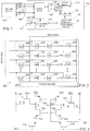
- FIG. 6 a block diagram of a portion of an integrated circuit device having a plurality of SRAM blocks is shown.
- a portion 602 of programmable resources is coupled by data lines 603 to a routing circuit 604 which provides an interface to a plurality of memory blocks 606.
- the plurality of memory blocks are shown here by way of example as 32 SRAM blocks.
- the routing circuit 604 is preferably dedicated interconnect elements for the plurality of memory blocks 606.
- the routing circuit 604 enables routing data to U input ports of the routing circuit (shown here as 8 data input ports coupled to corresponding data lines D 1 -D 8 ) and V output ports (where V may be 32 as shown here for example), where each of the input and output ports may have W bits per port.
- memory element 1002 which could be a DRAM for example, using dedicated routing circuits to enable the multiplexing of data, where the memory element 1002 could be DRAM 902 and memory elements 1004 and 1016 could be two or more of the SRAMs 924-930.
- the arrangement of elements of Fig. 17 partitions SRAMS into two groups, including BRAMs which may be 36 Kbyte memory elements, and the enhanced memory elements 1716 comprise blocks of memory which are larger than the BRAMs, and may be 36 Mb, for example.
- BRAMs which may be 36 Kbyte memory elements
- the enhanced memory elements 1716 comprise blocks of memory which are larger than the BRAMs, and may be 36 Mb, for example.
- the enhanced memory elements 1716 could be implemented using the arrangement of memory elements and dedicated routing interconnect elements as set forth above, and more particularly as shown in Figs. 6-8 or the arrangements of Figs. 6-8 as implemented in Fig. 9 .
- the LUT data input signals are supplied by the FPGA interconnect structure via input multiplexers, which may be implemented by programmable interconnect element 1811, and the LUT output signals are also supplied to the interconnect structure.
- Slice M also includes: output select multiplexers 1811A-1811D driving output terminals AMUX-DMUX; multiplexers 1812A-1812D driving the data input terminals of memory elements 1802A-1802D; combinational multiplexers 1816, 1818, and 1819; bounce multiplexer circuits 1822-1823; a circuit represented by inverter 1805 and multiplexer 1806 (which together provide an optional inversion on the input clock path); and carry logic having multiplexers 1814A-1814D, 1815A-1815D, 1820-1821 and exclusive OR gates 1813A-1813D.
- Fig. 19 could be used to implement the circuit of Fig. 9 , where the DRAM 902 is implemented as DRAM 1912, and the plurality of memory elements 924-930 are implemented as SRAMs or EDRAMs in the substrate 1906.
- the DRAM interface 922 and the programmable resources interface 932 may be implemented on the substrate 1906 or as a part of the interposer 1908.
Description
- The present invention relates generally to integrated circuit devices, and in particular, to an integrated circuit device having memory and a method of implementing memory in an integrated circuit device.
- The use of memory is an important aspect of almost any electronic device. There are different types of memory. For example, volatile memory is a type of memory which will retain values stored in the memory only when power is applied to the memory. When power is removed, the data stored in the memory will be lost over some period of time. In contrast, non-volatile memory is a type of memory whose data is not affected when power is removed.
- Different types of memory elements may have different properties. For example, memory elements may have different access times, power consumption, immunity to the effects of radiation, etc. Accordingly, memories can be selected not only based upon a desired operation of the memory, but operational qualities of a memory.
- Depending upon the functionality or operational qualities of the memory, a memory may be included on an integrated circuit device, or implemented separate from the integrated circuit device and accessed by the integrated circuit device. Providing a memory separate from an integrated circuit device may affect the operation of the overall circuit implementing the memory. Accordingly, there are various considerations when selecting both the type of memory and the locations of memory when implementing memory associated with an integrated circuit device.
-
US2009/072856 describes a system that includes a configurable memory controller, a memory interface, and a configurable high speed communications fabric. The configurable high speed communications fabric comprises a plurality of interconnect stations arranged in an array and is operable to implement a plurality of pipelined buses. The configurable memory controller is operably coupled to the configurable high speed communications fabric using a first interconnect station of the plurality of interconnect stations. The memory interface is operably coupled to the configurable high speed communications fabric using a second interconnect station of the plurality of interconnect stations. The plurality of interconnect stations are configured to satisfy a timing requirement of the memory interface. The configurable memory controller, the memory interface, and the configurable high speed communications fabric are associated with a configurable integrated circuit. An example of the system is a FPGA that includes one or more programmable logic blocks, one or more configurable special-purpose blocks, and one or more routing crossbars. Each programmable logic block may include one or more 4-input lookup tables and one or more configurable 1-bit sequential cells. A configurable special-purpose block implements a widely-used function. The routing crossbars form a two-dimensional routing network that provides configurable connections among the logic blocks and the special-purpose blocks. Each XBAR may be connected to the nearest-neighbor XBARs in four directions and to either a logic block or a special-purpose block. The special-purpose block can be a reconfigurable content addressable memory. -
US6467017 describes a programmable logic device that has embedded random access memory ("RAM") that can function equally well in either single-port or dual-port operation. The RAM is dual-port RAM whose read address inputs and write address inputs are both connected to a conductor bus via two different sparsely populated programmable interconnection resources. - Various aspects of the present invention are defined in the independent claims. Some preferred features are defined in the dependent claims.
- An integrated circuit device having memory is described. The integrated circuit device comprises programmable resources; programmable interconnect elements coupled to the programmable resources, the programmable interconnect elements enabling a communication of signals with the programmable resources; a plurality of memory blocks; and dedicated interconnect elements coupled to the plurality of memory blocks, the dedicated interconnect elements enabling access to the plurality of memory blocks.
- An integrated circuit device having memory according to an alternate arrangement comprises a dynamic random access memory (DRAM) block having a plurality of channels; a plurality of memory blocks; and dedicated interconnect elements coupled between the DRAM block and the plurality of memory blocks, the dedicated interconnect elements enabling routing data from any of the plurality of channels of the DRAM block to selected memory blocks of the plurality of memory blocks.
- A method of implementing memory in an integrated circuit device is also described. The method comprises implementing programmable resources coupled to programmable interconnect elements, the programmable interconnect elements enabling a communication of signals with the programmable resources; providing a plurality of memory blocks; and coupling dedicated interconnect elements to the plurality of memory blocks, the dedicated interconnect elements enabling access to the plurality of memory blocks.
-
-
Fig. 1 is a block diagram of an integrated circuit coupled to an external memory; -
Fig. 2 is a block diagram of a static random access memory (SRAM) block; -
Fig. 3 is a circuit diagram of a memory cell of the SRAM block ofFig. 2 ; -
Fig. 4 is a block diagram of a DRAM block; -
Fig. 5 is circuit diagram of a memory cell of the DRAM block ofFig. 4 ; -
Fig. 6 is a block diagram of a portion of an integrated circuit device having a plurality of SRAM blocks; -
Fig. 7 is a block diagram of a portion of an integrated circuit device coupled to a plurality of SRAM blocks and having separate read and write control; -
Fig. 8 is a block diagram of a portion of an integrated circuit device having a plurality of SRAM blocks having data and read and write control associated with a single crossbar switch; -
Fig. 9 is a block diagram of an integrated circuit device having a plurality of SRAM blocks and a DRAM block; -
Fig. 10 is a block diagram showing a circuit enabling the storage of data in queues of a DRAM; -
Fig. 11 is a block diagram showing a more detailed circuit enabling a packet buffering subsystem; -
Fig. 12 is a block diagram showing the implementation of SRAM blocks using different size memory arrays for head and tail portions; -
Fig. 13 is a block diagram showing the implementation of SRAM blocks having head and tail memory allocation; -
Fig. 14 is a block diagram showing the implementation of SRAM blocks having head and tail memory allocation and bypass channels; -
Fig. 15 is a block diagram of a crossbar switch; -
Fig. 16 is a block diagram of a system for programming a device having programmable resources; -
Fig. 17 is a block diagram of a device having programmable resources which may implement the circuits ofFigs. 1-15 ; -
Fig. 18 is a block diagram of a configurable logic element of the device ofFig. 17 ; and -
Fig. 19 is a block diagram of a multichip module integrated circuit device; and -
Fig. 20 is a flow chart showing a method of implementing memory in an integrated circuit device. - Turning first to
Fig. 1 , a block diagram of an integrated circuit coupled to an external memory is shown. In particular, anintegrated circuit device 102 is coupled to anexternal memory 104 by way ofcommunication links 106. The integrated circuit device could be any type of integrated circuit device, such as an application specific integrated circuit (ASIC) or an integrated circuit device having programmable resources, as will be described in more detail below. Theintegrated circuit device 102 comprises a control circuit 108 coupled to aconfiguration circuit 110. Theconfiguration circuit 110 may receive configuration data from theexternal memory 104 by way of the control circuit 108, or by way of an input/output (I/O) port 112. Theconfiguration circuit 110 is used to configure theprogrammable resources 114 of the integrated circuit device by providing configuration data to theconfiguration memory 116. Alternatively, the configuration data could be provided to the configuration memory directly by the control circuit 108. The control circuit 108 and theprogrammable resources 114 may also be coupled tointernal memory dedicated interconnect elements programmable resources 114, for enabling access to the memory elements. - As will be described in more detail below, the
internal memory - Turning now to
Fig. 2 , a block diagram of anSRAM block 200 is shown. TheSRAM block 200 ofFig. 2 may be a portion of theinternal memory 118, while theinternal memory 120 may be a DRAM block, for example, which will be described in more detail below in reference toFigs. 4 and 5 . TheSRAM block 200 comprises a plurality ofindividual memory cells 202, which may be arranged in a matrix. Columns of memory cells and acolumn decoder 204 are coupled to data lines and rows of memory cells are coupled to word lines to generate output data as an output of the DRAM. Accordingly, to write data to a cell, a word line associated with the cell is pulled high, and the desired data is coupled to the data line associated with the cell. To read data from a cell, the word line associated with a cell is pulled high, and the column decoder generates output values associated with the column in which the cell is located. - Turning now to
Fig. 3 , a circuit diagram of a memory cell of the SRAM memory block ofFig. 2 is shown. The memory cell includes an inverter having a p-channel transistor 302 with a source coupled to a reference power voltage, such as Vdd, and a drain coupled at a first node "Q" to a drain of an n-channel transistor 304, the source of which is coupled to a ground potential (Vss). The memory cell includes a second inverter having a p-channel transistor 306 with a source coupled to the reference voltage and a drain coupled at a second node "Q_b" to a drain of an n-channel transistor 308, the source of which is also coupled to ground. The first node "Q" is controlled by an n-channel transistor 310 coupled to receive an inverted word line (WL0_bar) signal at its gate which controls the receipt of input data on a bit line (BL) at the first node. The second node "Q_b" is controlled by another n-channel transistor 312 coupled to receive the inverted word line signal at its gate which controls the receipt of inverted input data at the second node Q_b.Transistors transistors Fig. 3 can operate twice as fast as a cell having 2 w/r ports by enabling accessing the memory on half clock cycles (i.e. the rising and falling edges of the clock). While the memory cell ofFig. 3 is shown by way of example, other memory cells could be employed. - Turning now to
Fig. 4 , a block diagram of a DRAM block is shown. The DRAM block ofFig. 4 could be a part of theexternal memory 104 or theinternal memory 120, as will be described in more detail below. TheDRAM block 400 comprises a plurality ofcells 402, each of which is coupled to anaddress decoder 404. Theaddress decoder 404 receivesaddress lines 406, and generates an address which is coupled to the plurality ofmemory cells 402 as is shown. Theaddress decoder 404 receives a chip enable signal, and each of thememory cells 402 receives a reference voltage Vref. Awrite block 410 enables the reading of data from or the writing of data to thememory cells 402. In particular, data provided by way ofdata lines 412 are written to an address provided to an address decoder if a write enable signal provided to thewrite block 410 enables writing to thememory cells 402 by way of thegates 414. If the write enable signal is not enabling writing to thememory cells 402, data coupled toinverters 416 is generated ondata lines 418. As will be described in more detail below, data stored in the cells of the DRAM block must be periodically refreshed to retain the data. - Turning now to
Fig. 5 , circuit diagram of a memory cell of the DRAM block ofFig. 4 is shown. In particular, afirst transistor 502 has adrain 504 coupled to a reference bit line and asource 506 coupled to acapacitor 508. Thetransistor 502 is controlled at a gate by a reference word line. Asecond transistor 514 has adrain 516 coupled to a bit line and asource 518 coupled to acapacitor 520. Thetransistor 514 is controlled at a gate by a word line. Data is written by pulling the word line high, and applying the desired value to be stored to the bit line to charge thecapacitor 520. In order to read data from the memory, thesense amp 526 will detect a difference between the voltage stored on thecapacitor 512 at the reference bit line and the voltage stored on thecapacitor 524 at the bit line to generate an output value. After the value of the bit line is determined, that value is re-written to the bit line by storing the appropriate charge on thecapacitor 524. That is, thecapacitor 524 is periodically recharged to maintain the correct value of data stored by the cell. While an individual DRAM memory cell is beneficial because it is smaller than the SRAM cell ofFig. 3 , the DRAM memory cell must be periodically refreshed to maintain the charge on the capacitor representing the stored data and may have a longer access time than the SRAM cell. - Turning now to
Fig. 6 , a block diagram of a portion of an integrated circuit device having a plurality of SRAM blocks is shown. Aportion 602 of programmable resources is coupled bydata lines 603 to arouting circuit 604 which provides an interface to a plurality of memory blocks 606. The plurality of memory blocks are shown here by way of example as 32 SRAM blocks. Therouting circuit 604 is preferably dedicated interconnect elements for the plurality of memory blocks 606. Therouting circuit 604 enables routing data to U input ports of the routing circuit (shown here as 8 data input ports coupled to corresponding data lines D1-D8) and V output ports (where V may be 32 as shown here for example), where each of the input and output ports may have W bits per port. That is, each individual input port of therouting circuit 604 corresponding to a data line may receive 288-bit data (which may 256 bit data and 32 overhead bits), and each output port may generate 288-bit data. For example, a representative one of the output ports is coupled by a correspondingdata line 605 to an input of a first memory block designatedSRAM 0. Therefore, data D1-D8 from each of the eight 288-bit input ports may be routed to one or more of 32 memory blocks by way of 32 288-bit output ports of therouting circuit 604. It should be understood that the data provided to the plurality of memory blocks according to the circuit arrangement ofFig. 6 could include data bits and control bits, where the control bits may include address bits for example. - A
second routing circuit 608 is coupled to outputs of the plurality of memory blocks 606 to receive data generated by the plurality of memory blocks. An output ofSRAM 0 at a correspondingrepresentative data line 607 is coupled to an input of therouting circuit 608.Output data lines 609 of therouting circuit 608 are coupled between corresponding output ports of therouting circuit 608 and asecond portion 610 of programmable resources. Therouting circuits Fig. 15 , and are preferably implemented as dedicated interconnect elements, rather than using shared routing elements which could be used by circuits other than thespecific portions output data lines 609 could also be multi-bit lines (e.g. 8 bit lines) which are coupled to receive corresponding 8-bit outputs at the outputs of the plurality of memory elements. Accordingly, the 8-bit outputs Q1-Q8 of 8 of the 32 SRAMS could be generated at the 8output data lines 609 of therouting circuit 608. Acontrol line 612 is used to route the various inputs to therouting circuit 604 to first predetermined memory blocks of the plurality of memory blocks 606. Similarly, acontrol line 614 is used to route outputs of second predetermined memory blocks to the 8 outputs ports of therouting circuit 608 and to theportion 610 of the programmable resources. By providing dedicated routing circuits and dedicated interconnects as inputs and outputs to the circuit, the speed of the SRAM access can be increased. That is, shared interconnect routing for a programmable logic device, while providing greater flexibility for the device, can be slow. In contrast, dedicated routing circuits, such as a crossbar switch, can operate at a system clock for the integrated circuit. - Turning now to
Fig. 7 , a block diagram of a portion of an integrated circuit device coupled to a plurality of SRAM blocks and having separate read and write control is shown. That is, the arrangement ofFig. 7 enables the separate routing of data bits and control bits by way of separate routing circuits, where the control bits include separate read and write control bits, including address bits for example. In particular, arouting circuit 702 is coupled to receive write control signals WC1WC8 from theprogrammable resources 602, where a representative one of a plurality of output ports of therouting circuit 702 is coupled by a control line 704 to a corresponding control signal input of a memory element of the plurality ofmemory elements 606, designated here asSRAM 0. Anotherrouting circuit 708 is coupled to receive data inputs D1-D8 at input ports of therouting circuit 708. Output ports of therouting circuit 708, shown here by a representative data line 710 of a plurality of data lines at corresponding output ports, are coupled to a first memory block, designated here asSRAM 0. Accordingly, therouting circuit 702 enables routing any pair of data and control signals to data and control inputs of one or more selected memory elements of the plurality ofmemory elements 606. - Routing circuits are also provided to read data from the plurality of memory blocks. A routing circuit 714 is coupled to receive control signals from the
portion 610 of the programmable resources, including read control signals RC1RC8. The routing circuit 714 enables routing the read control signals to selected memory blocks, where an output port of the routing circuit 714 is coupled by a control line to a memory (shown here as a representative control line 716 coupled to the last memory block, designated here as SRAM 31). Arouting circuit 718 is coupled to receive outputs from the plurality ofmemories 720, where arepresentative data line 720 provides data from an output of the last memory block to an input of therouting circuit 718. The data Q1-Q8 provided by the memory blocks 606 is provided by one of the eight outputs lines from therouting circuit 718 to theprogrammable resources 610. Control signals are provided by the programmable resources to the routing circuits. More particularly, write control signals are provided byprogrammable resources 602, by way ofcontrol lines routing circuits programmable resources 610, by way of 724 and 726, to therouting circuits 714 and 718, respectively. Alternatively, control signals may be provided by another element of the circuit, such as a processor of the circuit. - Turning now to
Fig. 8 , a block diagram of a portion of an integrated circuit device comprising a plurality of SRAM blocks having data and read and write control associated with a single crossbar switch is shown. Accordingly, both data D1-D8 and write control signals WC1-WC8 are provided to therouting circuit 802. For example, data D1 and write control signals WC1 are provided to therouting circuit 802 by representativesignal line pair 803. The signals on the signal line pair at corresponding input ports of therouting circuit 802 are then provided to a selected memory element (which could be, by way of example, SRAM 0) bysignal line pair 804. Read control signals RC1-RC8 are generated by theprogrammable resources 610 and coupled by control signal lines between theprogrammable resources 610 and the plurality ofmemory elements 606. By way of example, a representativecontrol signal line 810 couples a selected read control signal (which could be read control signal RC1 provided by way ofread control line 811 between an output port of theprogrammable resources 806 and an input port of the routing circuit 806) to a read input ofSRAM 0, and anoutput signal line 812 coupled to a data output of theSRAM 0 enables data from theSRAM 0 to be coupled to the programmable resources by way of therouting circuit 806. For example, the output data provided onoutput signal line 812 may be Q1 which is routed by therouting circuit 806 on asignal line 814 between an output port of therouting circuit 806 and a corresponding input port of theprogrammable resources 610. Control signals are provided bycontrol signal lines routing circuits - Turning now to
Fig. 9 , a block diagram of an integrated circuit device having a plurality of SRAMs and a DRAM is shown. According to the circuit arrangement ofFig. 9 , aDRAM 902 is coupled to anintegrated circuit 904. TheDRAM 902 comprises output channels 906-920, designated DRAM Channel 0 -DRAM Channel 7. ADRAM interface 922 enables data provided to theintegrated circuit 904 to be routed to one of a plurality of memory blocks 924-930, shown here as networked SRAMs (NSRAM 0 - NSRAM 3) which could be 4.5 megabyte memory arrays. That is, each of the networked SRAMs (NSRAM0-NSRAM3) could comprise 32 4Kx288 bit SRAMS, such asSRAMs 606. While the plurality of memory blocks 924-930 are shown as SRAMs, it should be understood that the plurality of memory blocks 924-930 generally have faster access time than theDRAM 902. For example, the memory blocks 924-930 could be eDRAMs, available from International Business Machines Corporation of Armonk, New York. Aprogrammable resource interface 932 is provided between the plurality of memory blocks 924-930 andprogrammable resources 934 to enable data and commands to be transferred between the memory blocks and theprogrammable resources 934. TheDRAM interface 922 and the programmable resources interface 932 are preferably dedicated interfaces, and could also be implemented using a crossbar switch, such as the crossbar switch ofFig. 15 . The plurality of memory blocks 924-930 and the correspondinginterfaces Figs. 6-8 , for example. While theDRAM 902 is shown separate from the integratecircuit 904, it should be understood that the DRAM could be implemented on the same integrated circuit die, or on a separate die on the same integrated circuit package, as will be described in more detail in reference toFig. 19 . - The arrangement of
Fig. 9 is beneficial because it allows greater efficiency in implementing memory in an integrated circuit. For example, without 100Mb of additional caching SRAMs on-die (such as SRAMs 924-930), theintegrated circuit device 904 could not support 400Gb/s packet buffering with bandwidth guarantee for up to 300 logical queues. These SRAM blocks must be on-die because there are insufficient package I/O pins in conventional devices to support the required bandwidth for external SRAM. Further, the SRAM width is matched to DRAM channel width (e.g. 256 bits per cycle), and the SRAM depth is sized to allow flexible allocation of memory capacity to memory ports by combining multiple such SRAMs into an even larger memory. For instance, with 1Mb building block SRAMs, 2Mb can be allocated to one cache and 10Mb can be allocated to a different cache. Too shallow of a building-block SRAM results in less density (i.e. bits per unit area), while too deep of a building-block SRAM limits flexibility for allocating memory capacity to memory ports. Particular applications of the circuit arrangements ofFig. 9 will be provided inFigs. 10-14 . - Turning now to
Fig. 10 , a block diagram shows a circuit enabling the storage of data in queues of a DRAM. An input data stream having data from a plurality of data packets is stored in amemory element 1002, which may comprise a plurality of logical FIFOs for example. Arouting circuit 1006 coupled to an output of thememory element 1004 enables routing of data associated with the data packets to corresponding queues 1008-1010 as shown. Asecond routing circuit 1014 routes data from outputs of the queues 1008-1010 to amemory element 1016. Accordingly, the circuit ofFig. 10 enables reading data from and writing data to a bulk storage element (e.g. memory element 1002), which could be a DRAM for example, using dedicated routing circuits to enable the multiplexing of data, where thememory element 1002 could beDRAM 902 andmemory elements - By way of example, the circuits of
Figs. 6-9 (implemented as shown inFig. 10 ) could be used as a packet buffer (between and input data stream and an output data stream) to hold Q logical flows of packets for up to Tc seconds at an input line rate of R' using a DRAM with a peak bandwidth of Ra, where a read rate Rw and write rate Rr have a combined (Rw + Rr) which is less than a peak bulk storage bandwidth Ra and a bulk storage capacity of TcR'. Accordingly, a buffer read rate of R" can be sustained with zero packet drop. As is apparent fromFig. 10 , memory blocks, shown here as queues, can be used to enable data from different packets (for example, the cross-hatched data inQueue 1, the shaded data inQueue 2 , or the unshaded data in Queue 3) to be stored, where routing circuits enable the routing of data from an input data stream to the bulk storage device, and from the bulk storage device to an output data stream. - Turning now to
Fig. 11 , a block diagram shows a more detailed circuit enabling a packet buffering subsystem. More particularly, thepacket buffering subsystem 1102 is coupled toinput logic 1104 for receiving input data Rin and output logic for generating output data Rout. Thepacket buffering subsystem 1102 comprises apacket buffer 1110 which is coupled to apacket buffer controller 1108. Thepacket buffer 1110 may be a DRAM, for example. Thepacket buffer controller 1108 comprises atail cache SRAM 1112 and ahead cache SRAM 1114 which are controlled by aqueueing coordinator 1116. Tail-head caching will be described in more detail below in reference toFigs. 12 and13 , and thequeueing coordinator 1116 will enable bypass of the DRAM will be described in more detail in reference toFig. 14 . - Turning now to
Fig. 12 , a block diagram shows the implementation of SRAM blocks using different size memory arrays for head and tail portions. In particular, various DRAM channels includingDRAM channel corresponding memory block separate tail portions 1202 andhead portions 1204, where the tail portion is generally smaller than the head portion. That is, because it may not be predictable when a queue is going to be accessed, and a next read may be for a queue which is being filled, it is necessary to make the head cache larger. As shown in the enlarged portion ofmemory block 926,certain memory elements 1206, designated by the dark shading, are memory elements for the tail caching, while the otherunshaded memory elements 1208 are memory elements of the head caching. The head cache is often much larger than the tail cache to enable low latency. - Turning now to
Fig. 13 , a block diagram shows the implementation of SRAM blocks having head and tail memory allocation. According to the embodiment ofFig. 13 , specific memory blocks, shown in dark shading, are designated as tail memory blocks, while the other memory blocks which are not shaded are head memory blocks. By way of example,SRAM 0 andSRAM 1 are tail caching memory blocks forchannel 0, while SRAM 2-SRAM 12 are head caching memory blocks forchannel 0, andSRAM 13 andSRAM 14 are tail memory blocks forchannel 1, while SRAM 15-SRAM 24 are head memory blocks forchannel 1. - Turning now to
Fig. 14 , a block diagram shows the implementation of SRAM blocks having head and tail memory allocation and bypass channels. In particular, various write signals for each ofchannel 1 andchannel 2 include a tail write command (Tail Write 0) and a head write command (Head Write 0) forchannel 0 and a tail write command (Tail Write 1) and a head write command (Head Write 1) forchannel 1. Also shown are tail read (Tail Read 0) and head read (Head Read 0) values forchannel 0, and tail read (Tail Read 1) and head read (Head Read 1) values forchannel 1. Bypasses are provided from the tail memory elements to the head memory elements for each ofchannel 1 andchannel 2. Accordingly,Fig. 14 provides an example implementation of tail-head caching using the arrangement of elements ofFigs. 6-13 , for example. - Turning now to
Fig. 15 , a block diagram of a crossbar switch is shown. In particular, each multiplexer of a plurality of multiplexers 1502-1510 is coupled to receive each of the inputs, designated Di0-Di3, and generate an output for each of the multiplexers. Multiplexer 1502 generates an output Do0,multiplexer 1504 generates an output Do1,multiplexer 1506 generates an output Do2,multiplexer 1508 generates an output Do3,multiplexer 1510 generates an output Do4 based upon selection signals provided to the plurality of multiplexers. An enlarged section ofmultiplexer 1510 shows transistors 1512 to 1518 coupled to the inputs for receiving signals Di0-Di3, respectively, to an output signal Do4 at a common node based upon the selection signals S1-S4. While the multiplexer arrangement ofFig. 15 is shown by way of example, it should be understood that other arrangements of transistors could be implemented to achieve the multiplexing functionality. As is apparent fromFig. 15 , the crossbar switch could be selected to route a given number of signals to a fewer number of outputs or a given number of signals to a greater number of outputs. Further, the selection signal of the crossbar switch can be dynamically changed, in contrast to multiplexer control signals for general programmable interconnects of a programmable logic device which must be provided as configuration data and changed by a configuration process. Accordingly, the crossbar switch ofFig. 15 could be used for any of the routing circuits ofFigs. 6-14 , or any other circuit set forth above which could be implemented in a crossbar switch. - Turning now to
Fig. 16 , a block diagram of a system for programming a device having programmable resources according to an embodiment is shown. In particular, acomputer 1602 is coupled to receive acircuit design 1604 from amemory 1606, and generate a configuration bitstream which is stored in thenon-volatile memory 1606. As will be described in more detail below, the circuit design may be a high level design, such as a circuit design defined in a hardware description language (HDL). Also, the computer may be configured to run software that generates a configuration bitstream which is stored in thenon-volatile memory 1608 and provided to anintegrated circuit 1610 which may be a programmable integrated circuit, such as the integrated circuit described below inFig. 17 . - Turning now to
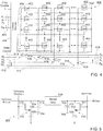
Fig. 17 , a block diagram of a device having programmable resources including the circuits ofFigs. 2-16 is shown. While devices having programmable resources may be implemented in any type of integrated circuit device, such as an application specific integrated circuit (ASIC) having programmable resources, other devices comprise dedicated programmable logic devices (PLDs). One type of PLD is the Complex Programmable Logic Device (CPLD). A CPLD includes two or more "function blocks" connected together and to input/output (I/O) resources by an interconnect switch matrix. Each function block of the CPLD includes a two-level AND/OR structure similar to that used in a Programmable Logic Array (PLA) or a Programmable Array Logic (PAL) device. Another type of PLD is a field programmable gate array (FPGA). In a typical FPGA, an array of configurable logic blocks (CLBs) is coupled to programmable input/output blocks (lOBs). The CLBs and lOBs are interconnected by a hierarchy of programmable routing resources. These CLBs, lOBs, and programmable routing resources are customized by loading a configuration bitstream, typically from off-chip memory, into configuration memory cells of the FPGA. For both of these types of programmable logic devices, the functionality of the device is controlled by configuration data bits of a configuration bitstream provided to the device for that purpose. The configuration data bits may be stored in volatile memory (e.g., static memory cells, as in FPGAs and some CPLDs), in non-volatile memory (e.g., Flash memory, as in some CPLDs), or in any other type of memory cell. - The device of
Fig. 17 comprises an FPGA architecture 1400 having a large number of different programmable tiles including multi-gigabit transceivers (MGTs) 1701,CLBs 1702, random access memory blocks (BRAMs) 1703, input/output blocks (lOBs) 1704, configuration and clocking logic (CONFIG/CLOCKS) 1705, digital signal processing blocks (DSPs) 1706, specialized input/output blocks (I/O) 1707 (e.g., configuration ports and clock ports), and otherprogrammable logic 1708 such as digital clock managers, analog-to-digital converters, system monitoring logic, and so forth. Some FPGAs also include dedicated processor blocks (PROC) 1710, which may be used to implement a software application, for example. - In some FPGAs, each programmable tile includes a programmable interconnect element (INT) 1711 having standardized connections to and from a corresponding interconnect element in each adjacent tile. Therefore, the programmable interconnect elements taken together implement the programmable interconnect structure for the illustrated FPGA. The
programmable interconnect element 1711 also includes the connections to and from the programmable logic element within the same tile, as shown by the examples included at the top ofFig. 17 . - For example, a
CLB 1702 may include a configurable logic element (CLE) 1712 that may be programmed to implement user logic plus a singleprogrammable interconnect element 1711. ABRAM 1703 may include a BRAM logic element (BRL) 1713 in addition to one or more programmable interconnect elements. The BRAM includes dedicated memory separate from the distributed RAM of a configuration logic block. Typically, the number of interconnect elements included in a tile depends on the height of the tile. In the pictured embodiment, a BRAM tile has the same height as five CLBs, but other numbers may also be used. ADSP tile 1706 may include a DSP logic element (DSPL) 1714 in addition to an appropriate number of programmable interconnect elements. AnIOB 1704 may include, for example, two instances of an input/output logic element (IOL) 1715 in addition to one instance of theprogrammable interconnect element 171 1 . The location of connections of the device is controlled by configuration data bits of a configuration bitstream provided to the device for that purpose. The programmable interconnects, in response to bits of a configuration bitstream, enable connections comprising interconnect lines to be used to couple the various signals to the circuits implemented in programmable logic, or other circuits such as BRAMs or the processor. - In the pictured embodiment, a columnar area near the center of the die is used for configuration, clock, and other control logic. The config/clock distribution regions 1709 extending from this column are used to distribute the clocks and configuration signals across the breadth of the FPGA. Some FPGAs utilizing the architecture illustrated in
Fig. 17 include additional logic blocks that disrupt the regular columnar structure making up a large part of the FPGA. The additional logic blocks may be programmable blocks and/or dedicated logic. For example, theprocessor block PROC 1710 shown inFig. 17 spans several columns of CLBs and BRAMs. - The FPGA of
Fig. 17 further comprises enhancedmemory elements 1716 which are larger than theBRAMs 1703. Theenhanced memory elements 1716 may comprise an SRAM block and dedicated interconnect elements, separate from the various interconnect elements described in reference to blocks of thecircuit 1700, enabling access to memory elements of the enhanced memory elements by blocks of thecircuit 1700 or devices external to thecircuit 1700. - Note that
Fig. 17 is intended to illustrate only an exemplary FPGA architecture. The numbers of logic blocks in a column, the relative widths of the columns, the number and order of columns, the types of logic blocks included in the columns, the relative sizes of the logic blocks, and the interconnect/logic implementations included at the top ofFig. 17 are purely exemplary. For example, in an actual FPGA more than one adjacent column of CLBs is typically included wherever the CLBs appear in order to facilitate the efficient implementation of user logic. While the embodiment ofFig. 17 relates to an integrated circuit having programmable resources, it should be understood that the circuits and methods set forth in more detail below could be implemented in any type of ASIC. - Accordingly, the arrangement of elements of
Fig. 17 partitions SRAMS into two groups, including BRAMs which may be 36 Kbyte memory elements, and theenhanced memory elements 1716 comprise blocks of memory which are larger than the BRAMs, and may be 36 Mb, for example. By providing the deeper memories of the enhancedmemory elements 1716, more bits are provided per unit area, and there is no need to cascade multiple BRAMS to achieve a larger memory. Theenhanced memory elements 1716 could be implemented using the arrangement of memory elements and dedicated routing interconnect elements as set forth above, and more particularly as shown inFigs. 6-8 or the arrangements ofFigs. 6-8 as implemented inFig. 9 . - Turning now to
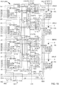
Fig. 18 , block diagram of a configurable logic element of the device ofFig. 17 is shown. In particular,Fig. 18 illustrates in simplified form a configurable logic element of aconfiguration logic block 1702 ofFig. 17 . In the embodiment ofFig. 18 ,slice M 1801 includes four lookup tables (LUTMs) 1801A-1801D, each driven by six LUT data input terminals A1-A6, B1-B6, C1-C6, and D1-D6 and each providing two LUT output signals O5 and O6. The O6 output terminals from LUTs 1801A-1801D drive slice output terminals A-D, respectively. The LUT data input signals are supplied by the FPGA interconnect structure via input multiplexers, which may be implemented by programmable interconnect element 1811, and the LUT output signals are also supplied to the interconnect structure. Slice M also includes: outputselect multiplexers 1811A-1811D driving output terminals AMUX-DMUX; multiplexers 1812A-1812D driving the data input terminals of memory elements 1802A-1802D;combinational multiplexers inverter 1805 and multiplexer 1806 (which together provide an optional inversion on the input clock path); and carry logic having multiplexers 1814A-1814D, 1815A-1815D, 1820-1821 and exclusive OR gates 1813A-1813D. All of these elements are coupled together as shown inFig. 18 . Where select inputs are not shown for the multiplexers illustrated inFig. 18 , the select inputs are controlled by configuration memory cells. That is, configuration bits of the configuration bitstream stored in configuration memory cells are coupled to the select inputs of the multiplexers to select the correct inputs to the multiplexers. These configuration memory cells, which are well known, are omitted fromFig. 18 for clarity, as well as from other selected figures herein. - In the pictured embodiment, each memory element 1802A-1802D may be programmed to function as a synchronous or asynchronous flip-flop or latch. The selection between synchronous and asynchronous functionality is made for all four memory elements in a slice by programming Sync/
Asynch selection circuit 1803. When a memory element is programmed so that the S/R (set/reset) input signal provides a set function, the REV input terminal provides the reset function. When the memory element is programmed so that the S/R input signal provides a reset function, the REV input terminal provides the set function. Memory elements 1802A-1802D are clocked by a clock signal CK, which may be provided by a global clock network or by the interconnect structure, for example. Such programmable memory elements are well known in the art of FPGA design. Each memory element 1802A-1802D provides a registered output signal AQ-DQ to the interconnect structure. Because each LUT 1801A-1801D provides two output signals, 05 and 06, the LUT may be configured to function as two 5-input LUTs with five shared input signals (IN1-IN5), or as one 6-input LUT having input signals IN1-IN6. - In the embodiment of
Fig. 18 , each LUTM 1801A-1801D may function in any of several modes. When in lookup table mode, each LUT has six data input signals IN1-IN6 that are supplied by the FPGA interconnect structure via input multiplexers. One of 64 data values is programmably selected from configuration memory cells based on the values of signals IN1-IN6. When in RAM mode, each LUT functions as a single 64-bit RAM or two 32-bit RAMs with shared addressing. The RAM write data is supplied to the 64-bit RAM via input terminal DI1 (viamultiplexers 1817A-1817C forLUTs 1801 A-1801 C), or to the two 32-bit RAMs via input terminals DI1 and DI2. RAM write operations in the LUT RAMs are controlled by clock signal CK frommultiplexer 1806 and by write enable signal WEN frommultiplexer 1807, which may selectively pass either the clock enable signal CE or the write enable signal WE. In shift register mode, each LUT functions as two 16-bit shift registers, or with the two 16-bit shift registers coupled in series to create a single 32-bit shift register. The shift-in signals are provided via one or both of input terminals DI1 and DI2. The 16-bit and 32-bit shift out signals may be provided through the LUT output terminals, and the 32-bit shift out signal may also be provided more directly via LUT output terminal MC31. The 32-bit shift out signal MC31 of LUT 1801A may also be provided to the general interconnect structure for shift register chaining, via output select multiplexer 1811D and CLE output terminal DMUX. Accordingly, the circuits and methods set forth above may be implemented in a device such as the devices ofFigs. 17 and18 , or any other suitable device. - According to the embodiment of
Fig. 19 , acircuit board 1902, such as a printed circuit board, is configured to receive a multi-dieintegrated circuit 1904. The multi-dieintegrated circuit 1904 comprises asubstrate 1906 coupled to receive aninterposer circuit 1908. Theinterposer 1908 enables coupling multiple integrated circuit chips or die, such asFPGA chips 1910 and aDRAM chip 1912 circuits, to thesubstrate 1906.Solder balls 1914 enabling enable coupling signals from the various chips to thecircuit board 1902 by way ofvarious interconnects 1916, such as through silicon vias (TSVs).Interconnects 1918 also enable the routing of signals between the various chips of the multi-die integrated circuit. Theinterposer circuit 1908 may be a silicon substrate with various metal layers comprising interconnect elements enabling the routing of signals between the FPGA chips and the DRAM chip or between one of the chips and thesubstrate 1906. However, the interposer circuit could be any material having conductive elements which enable routing signals as shown. While all of the circuits of theFPGA chips 1910 and theDRAM chip 1912 could be implemented on a single die, the embodiment ofFig. 19 enables more efficiently implementing the various circuits ofFPGA chips 1910 and theDRAM chip 1912. For example, some circuits may be more efficiently implemented in an integrated circuit chip manufactured according to one process, such as a process forming transistors of a certain dimension, while other circuits may be implemented more efficiently in an integrated circuit chip manufactured according to another process. Accordingly, the arrangement ofFig. 19 could be used to implement the circuit ofFig. 9 , where theDRAM 902 is implemented asDRAM 1912, and the plurality of memory elements 924-930 are implemented as SRAMs or EDRAMs in thesubstrate 1906. TheDRAM interface 922 and the programmable resources interface 932 may be implemented on thesubstrate 1906 or as a part of theinterposer 1908. - Turning now to
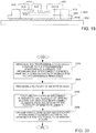
Fig. 20 , a flow chart shows a method of implementing memory in an integrated circuit device. In particular, programmable resources coupled to the programmable interconnect elements are implemented at ablock 2002, wherein the programmable interconnect elements enable the communication of signals with the programmable resources. The programmable interconnects could be the interconnect elements associated with lOBs or CLEs ofFig. 17 , for example. A plurality of memory blocks is provided at ablock 2004, and dedicated interconnect elements are coupled to the plurality of memory blocks at ablock 2006. The plurality of memory blocks may be the enhancedmemory elements 1716 ofFig. 17 , for example. A DRAM block may be implemented at ablock 2008, where dedicated interconnect elements may be implemented between the DRAM block and the plurality of memory blocks. The various elements of the method ofFig. 20 may be implemented using the circuits ofFigs. 1-19 as described, or using some other suitable circuits. While specific elements of the method are described, it should be understood that additional elements of the method, or additional details related to the elements 2002-2008, could be implemented according to the disclosure ofFigs. 1-19 . - It can therefore be appreciated that a new integrated circuit device having memory and method of implementing memory in an integrated circuit device has been described. It will be appreciated by those skilled in the art that numerous alternatives and equivalents will be seen to exist which incorporate the disclosed invention. As a result, the invention is not to be limited by the foregoing embodiments, but only by the following claims.
Claims (11)
- An integrated circuit device having memory, the integrated circuit device comprising:programmable resources (602) having a first plurality of data lines (603);programmable interconnect elements (1704) coupled to the programmable resources (602), the programmable interconnect elements enabling a communication of signals with the programmable resources;a plurality of memory blocks (606); anda dedicated interconnect element (604) coupled between the programmable resources (602) and each memory block of the plurality of memory blocks to enable the multiplexing of data from the first plurality of data lines (605), the dedicated interconnect element (604) having a first plurality of inputs and a second plurality of outputs and enabling access to each memory block (606) of the plurality of memory blocks;wherein each input of the first plurality of inputs of the dedicated interconnect element is coupled to a corresponding data line of the first plurality of data lines of the programmable resources, and each output of the second plurality of outputs of the dedicated interconnect element is coupled to a data line of a second plurality of data lines that is coupled to a corresponding memory block of the plurality of memory blocks; and whereinthe programmable resources (602) comprise a plurality of SRAM blocks each having a first memory size, and each memory block of the plurality of memory blocks is an SRAM block having a second memory size which is larger than the first memory size.
- The integrated circuit device of claim 1 wherein the plurality of memory blocks (606) comprises a plurality of SRAM blocks.
- The integrated circuit device of claim 1 or claim 2 wherein the dedicated interconnect element (604) comprises a crossbar switch.
- The integrated circuit device of any of claims 1-3 further comprising output interconnect elements (609) coupled between the plurality of memory blocks (606) and the programmable resources (610).
- The integrated circuit device of any of claims 1-4 wherein the programmable resources (602) comprise a DRAM block, and the dedicated interconnect element enables a communication of signals between the DRAM block and the plurality of memory blocks.
- The integrated circuit device of any of claims 1-5 wherein the DRAM block is on a first die of the integrated circuit device and the programmable resources are on a second die of the integrated circuit device.
- A method of implementing a memory in an integrated circuit device, the method comprising:implementing programmable resources (602) having a first plurality of data lines (603) and coupled to programmable interconnect elements (1704), the programmable interconnect elements (1704) enabling a communication of signals with the programmable resources (602);providing a plurality of memory blocks (606); andcoupling a dedicated interconnect element (604) between the programmable recourses (602) and each memory block of the plurality of memory blocks (606) to enable the multiplexing of data from the first plurality of data lines (605), the dedicated interconnect element (604) having a first plurality of inputs and a second plurality of outputs and enabling access to each memory block (606) of the plurality of memory blocks;wherein each input of the first plurality of inputs of the dedicated interconnect element is coupled to a corresponding data line of the first plurality of data lines of the programmable resources, and each output of the second plurality of outputs of the dedicated interconnect element is coupled to a data line of a second plurality of data lines that is coupled to a corresponding memory block of the plurality of memory blocks; and whereinthe implementing of the programmable resources (602) comprises implementing a first plurality of SRAM blocks each having a first memory size, and providing a plurality of memory blocks comprises providing a plurality of SRAM blocks each having a second memory size which is larger than the first memory size.
- The method of claim 7 wherein coupling a dedicated interconnect element between the plurality of memory blocks comprises providing the dedicated interconnect element separate from the programmable interconnect elements.
- The method of any of claims 7-8 wherein coupling a dedicated interconnect element to the plurality of memory blocks comprises coupling a crossbar switch to the plurality of memory blocks.
- The method of any of claims 7-9 wherein the programmable resources comprise a DRAM block and the dedicated interconnect element comprises a second crossbar switch between the DRAM block and the plurality of memory blocks.
- The method of any of claims 7-10 wherein implementing programmable resources comprises implementing programmable resources on a first die of the integrated circuit device and implementing a DRAM block comprises implementing a DRAM block on a second die of the integrated circuit device.
Applications Claiming Priority (2)
| Application Number | Priority Date | Filing Date | Title |
|---|---|---|---|
| US13/789,313 US9153292B2 (en) | 2013-03-07 | 2013-03-07 | Integrated circuit devices having memory and methods of implementing memory in an integrated circuit device |
| PCT/US2014/021404 WO2014138479A1 (en) | 2013-03-07 | 2014-03-06 | Integrated circuit devices having memory and methods of implementing memory in an integrated circuit device |
Publications (2)
| Publication Number | Publication Date |
|---|---|
| EP2965429A1 EP2965429A1 (en) | 2016-01-13 |
| EP2965429B1 true EP2965429B1 (en) | 2018-12-26 |
Family
ID=50442621
Family Applications (1)
| Application Number | Title | Priority Date | Filing Date |
|---|---|---|---|
| EP14716076.6A Active EP2965429B1 (en) | 2013-03-07 | 2014-03-06 | Integrated circuit devices having memory and methods of implementing memory in an integrated circuit device |
Country Status (6)
| Country | Link |
|---|---|
| US (1) | US9153292B2 (en) |
| EP (1) | EP2965429B1 (en) |
| JP (1) | JP6573834B2 (en) |
| KR (1) | KR102178768B1 (en) |
| CN (1) | CN105144585B (en) |
| WO (1) | WO2014138479A1 (en) |
Families Citing this family (27)
| Publication number | Priority date | Publication date | Assignee | Title |
|---|---|---|---|---|
| US9431095B1 (en) | 2014-12-10 | 2016-08-30 | Xilinx, Inc. | High-density integrated circuit memory |
| EP3411953B1 (en) * | 2016-02-02 | 2021-03-03 | Xilinx, Inc. | Active-by-active programmable device |
| US10331601B2 (en) * | 2016-04-15 | 2019-06-25 | Infinera Corporation | Systems, apparatus, and methods for efficient space to time conversion of OTU multiplexed signal |
| CN109564914B (en) * | 2016-08-15 | 2020-06-30 | 赛灵思公司 | Independent interface for Stacked Silicon Interconnect (SSI) technology integration |
| US11625523B2 (en) | 2016-12-14 | 2023-04-11 | iCometrue Company Ltd. | Logic drive based on standard commodity FPGA IC chips |
| TW202404049A (en) | 2016-12-14 | 2024-01-16 | 成真股份有限公司 | Logic drive based on standard commodity fpga ic chips |
| US10447274B2 (en) | 2017-07-11 | 2019-10-15 | iCometrue Company Ltd. | Logic drive based on standard commodity FPGA IC chips using non-volatile memory cells |
| JP2019033327A (en) | 2017-08-04 | 2019-02-28 | 株式会社東芝 | Semiconductor integrated circuit |
| US10957679B2 (en) | 2017-08-08 | 2021-03-23 | iCometrue Company Ltd. | Logic drive based on standardized commodity programmable logic semiconductor IC chips |
| US10630296B2 (en) * | 2017-09-12 | 2020-04-21 | iCometrue Company Ltd. | Logic drive with brain-like elasticity and integrality based on standard commodity FPGA IC chips using non-volatile memory cells |
| US10079211B1 (en) * | 2017-09-28 | 2018-09-18 | Intel Corporation | Modular interconnection repair of multi-die package |
| US10608642B2 (en) | 2018-02-01 | 2020-03-31 | iCometrue Company Ltd. | Logic drive using standard commodity programmable logic IC chips comprising non-volatile radom access memory cells |
| US10623000B2 (en) * | 2018-02-14 | 2020-04-14 | iCometrue Company Ltd. | Logic drive using standard commodity programmable logic IC chips |
| US10608638B2 (en) | 2018-05-24 | 2020-03-31 | iCometrue Company Ltd. | Logic drive using standard commodity programmable logic IC chips |
| US10892011B2 (en) | 2018-09-11 | 2021-01-12 | iCometrue Company Ltd. | Logic drive using standard commodity programmable logic IC chips comprising non-volatile random access memory cells |
| US11309334B2 (en) | 2018-09-11 | 2022-04-19 | iCometrue Company Ltd. | Logic drive using standard commodity programmable logic IC chips comprising non-volatile random access memory cells |
| US10937762B2 (en) | 2018-10-04 | 2021-03-02 | iCometrue Company Ltd. | Logic drive based on multichip package using interconnection bridge |
| US11616046B2 (en) | 2018-11-02 | 2023-03-28 | iCometrue Company Ltd. | Logic drive based on chip scale package comprising standardized commodity programmable logic IC chip and memory IC chip |
| US11211334B2 (en) | 2018-11-18 | 2021-12-28 | iCometrue Company Ltd. | Logic drive based on chip scale package comprising standardized commodity programmable logic IC chip and memory IC chip |
| US10642946B2 (en) * | 2018-12-28 | 2020-05-05 | Intel Corporation | Modular periphery tile for integrated circuit device |
| US10804255B1 (en) * | 2019-05-10 | 2020-10-13 | Xilinx, Inc. | Circuit for and method of transmitting a signal in an integrated circuit device |
| US10985154B2 (en) | 2019-07-02 | 2021-04-20 | iCometrue Company Ltd. | Logic drive based on multichip package comprising standard commodity FPGA IC chip with cryptography circuits |
| US11227838B2 (en) | 2019-07-02 | 2022-01-18 | iCometrue Company Ltd. | Logic drive based on multichip package comprising standard commodity FPGA IC chip with cooperating or supporting circuits |
| US10797037B1 (en) | 2019-07-15 | 2020-10-06 | Xilinx, Inc. | Integrated circuit device having a plurality of stacked dies |
| US11887930B2 (en) | 2019-08-05 | 2024-01-30 | iCometrue Company Ltd. | Vertical interconnect elevator based on through silicon vias |
| US11637056B2 (en) | 2019-09-20 | 2023-04-25 | iCometrue Company Ltd. | 3D chip package based on through-silicon-via interconnection elevator |
| US11600526B2 (en) | 2020-01-22 | 2023-03-07 | iCometrue Company Ltd. | Chip package based on through-silicon-via connector and silicon interconnection bridge |
Family Cites Families (12)
| Publication number | Priority date | Publication date | Assignee | Title |
|---|---|---|---|---|
| JPH07321640A (en) * | 1994-05-30 | 1995-12-08 | Nippon Telegr & Teleph Corp <Ntt> | Programmable logic circuit |
| US6072741A (en) * | 1997-04-01 | 2000-06-06 | Ramtron International Corporation | First-in, first-out integrated circuit memory device incorporating a retransmit function |
| US6181159B1 (en) | 1997-05-06 | 2001-01-30 | Altera Corporation | Integrated circuit incorporating a programmable cross-bar switch |
| US6467017B1 (en) | 1998-06-23 | 2002-10-15 | Altera Corporation | Programmable logic device having embedded dual-port random access memory configurable as single-port memory |
| US6350653B1 (en) | 2000-10-12 | 2002-02-26 | International Business Machines Corporation | Embedded DRAM on silicon-on-insulator substrate |
| JP3553519B2 (en) * | 2001-04-16 | 2004-08-11 | 三菱電機株式会社 | Programmable logic circuit device |
| US7076595B1 (en) * | 2001-05-18 | 2006-07-11 | Xilinx, Inc. | Programmable logic device including programmable interface core and central processing unit |
| JP4191218B2 (en) * | 2006-10-12 | 2008-12-03 | エルピーダメモリ株式会社 | Memory circuit and semiconductor device |
| US9071246B2 (en) | 2007-09-14 | 2015-06-30 | Agate Logic, Inc. | Memory controller for heterogeneous configurable integrated circuits |
| JP5163306B2 (en) * | 2008-06-19 | 2013-03-13 | 富士通セミコンダクター株式会社 | Dynamic reconfiguration circuit and data transmission control method |
| US8058897B1 (en) * | 2010-06-28 | 2011-11-15 | Xilinx, Inc. | Configuration of a multi-die integrated circuit |
| US8693235B2 (en) * | 2011-12-06 | 2014-04-08 | Taiwan Semiconductor Manufacturing Company, Ltd. | Methods and apparatus for finFET SRAM arrays in integrated circuits |
-
2013
- 2013-03-07 US US13/789,313 patent/US9153292B2/en active Active
-
2014
- 2014-03-06 JP JP2015561680A patent/JP6573834B2/en active Active
- 2014-03-06 WO PCT/US2014/021404 patent/WO2014138479A1/en active Application Filing
- 2014-03-06 KR KR1020157027772A patent/KR102178768B1/en active IP Right Grant
- 2014-03-06 EP EP14716076.6A patent/EP2965429B1/en active Active
- 2014-03-06 CN CN201480012875.1A patent/CN105144585B/en active Active
Non-Patent Citations (1)
| Title |
|---|
| None * |
Also Published As
| Publication number | Publication date |
|---|---|
| WO2014138479A1 (en) | 2014-09-12 |
| JP2016516331A (en) | 2016-06-02 |
| KR20150126400A (en) | 2015-11-11 |
| JP6573834B2 (en) | 2019-09-11 |
| KR102178768B1 (en) | 2020-11-13 |
| CN105144585B (en) | 2018-08-17 |
| US20140254232A1 (en) | 2014-09-11 |
| US9153292B2 (en) | 2015-10-06 |
| EP2965429A1 (en) | 2016-01-13 |
| CN105144585A (en) | 2015-12-09 |
Similar Documents
| Publication | Publication Date | Title |
|---|---|---|
| EP2965429B1 (en) | Integrated circuit devices having memory and methods of implementing memory in an integrated circuit device | |
| KR102446825B1 (en) | Circuits and methods for controlling operation of a hybrid memory system | |
| US6430088B1 (en) | Embedded static random access memory for field programmable gate array | |
| JP6564375B2 (en) | Memory configuration for realizing a high-throughput key-value store | |
| US7116131B1 (en) | High performance programmable logic devices utilizing dynamic circuitry | |
| US6038627A (en) | SRAM bus architecture and interconnect to an FPGA | |
| US6462577B1 (en) | Configurable memory structures in a programmable logic device | |
| EP2917844B1 (en) | Configurable embedded memory system | |
| US7202697B1 (en) | Programmable logic block having improved performance when functioning in shift register mode | |
| US8185861B2 (en) | Variable sized soft memory macros in structured cell arrays, and related methods | |
| US8390319B2 (en) | Programmable logic fabric | |
| US9811628B1 (en) | Metal configurable register file | |
| Senhadji-Navarro et al. | Performance evaluation of RAM-based implementation of finite state machines in FPGAs | |
| US7196963B1 (en) | Address isolation for user-defined configuration memory in programmable devices | |
| US7221185B1 (en) | Method and apparatus for memory block initialization | |
| Priadarshini et al. | Low power reconfigurable FPGA based on SRAM | |
| Miyamoto et al. | A 1.6 mm 2 4,096 logic elements multi-context FPGA core in 90nm CMOS | |
| Ngai et al. | A new generation of ORCA FPGA with enhanced features and performance |
Legal Events
| Date | Code | Title | Description |
|---|---|---|---|
| PUAI | Public reference made under article 153(3) epc to a published international application that has entered the european phase |
Free format text: ORIGINAL CODE: 0009012 |
|
| 17P | Request for examination filed |
Effective date: 20150824 |
|
| AK | Designated contracting states |
Kind code of ref document: A1 Designated state(s): AL AT BE BG CH CY CZ DE DK EE ES FI FR GB GR HR HU IE IS IT LI LT LU LV MC MK MT NL NO PL PT RO RS SE SI SK SM TR |
|
| AX | Request for extension of the european patent |
Extension state: BA ME |
|
| DAX | Request for extension of the european patent (deleted) | ||
| STAA | Information on the status of an ep patent application or granted ep patent |
Free format text: STATUS: EXAMINATION IS IN PROGRESS |
|
| 17Q | First examination report despatched |
Effective date: 20170502 |
|
| GRAP | Despatch of communication of intention to grant a patent |
Free format text: ORIGINAL CODE: EPIDOSNIGR1 |
|
| STAA | Information on the status of an ep patent application or granted ep patent |
Free format text: STATUS: GRANT OF PATENT IS INTENDED |
|
| INTG | Intention to grant announced |
Effective date: 20180711 |
|
| GRAS | Grant fee paid |
Free format text: ORIGINAL CODE: EPIDOSNIGR3 |
|
| GRAA | (expected) grant |
Free format text: ORIGINAL CODE: 0009210 |
|
| STAA | Information on the status of an ep patent application or granted ep patent |
Free format text: STATUS: THE PATENT HAS BEEN GRANTED |
|
| AK | Designated contracting states |
Kind code of ref document: B1 Designated state(s): AL AT BE BG CH CY CZ DE DK EE ES FI FR GB GR HR HU IE IS IT LI LT LU LV MC MK MT NL NO PL PT RO RS SE SI SK SM TR |
|
| REG | Reference to a national code |
Ref country code: GB Ref legal event code: FG4D |
|
| REG | Reference to a national code |
Ref country code: CH Ref legal event code: EP |
|
| REG | Reference to a national code |
Ref country code: AT Ref legal event code: REF Ref document number: 1082828 Country of ref document: AT Kind code of ref document: T Effective date: 20190115 |
|
| REG | Reference to a national code |
Ref country code: DE Ref legal event code: R096 Ref document number: 602014038571 Country of ref document: DE |
|
| REG | Reference to a national code |
Ref country code: IE Ref legal event code: FG4D |
|
| PG25 | Lapsed in a contracting state [announced via postgrant information from national office to epo] |
Ref country code: HR Free format text: LAPSE BECAUSE OF FAILURE TO SUBMIT A TRANSLATION OF THE DESCRIPTION OR TO PAY THE FEE WITHIN THE PRESCRIBED TIME-LIMIT Effective date: 20181226 Ref country code: LT Free format text: LAPSE BECAUSE OF FAILURE TO SUBMIT A TRANSLATION OF THE DESCRIPTION OR TO PAY THE FEE WITHIN THE PRESCRIBED TIME-LIMIT Effective date: 20181226 Ref country code: NO Free format text: LAPSE BECAUSE OF FAILURE TO SUBMIT A TRANSLATION OF THE DESCRIPTION OR TO PAY THE FEE WITHIN THE PRESCRIBED TIME-LIMIT Effective date: 20190326 Ref country code: BG Free format text: LAPSE BECAUSE OF FAILURE TO SUBMIT A TRANSLATION OF THE DESCRIPTION OR TO PAY THE FEE WITHIN THE PRESCRIBED TIME-LIMIT Effective date: 20190326 Ref country code: FI Free format text: LAPSE BECAUSE OF FAILURE TO SUBMIT A TRANSLATION OF THE DESCRIPTION OR TO PAY THE FEE WITHIN THE PRESCRIBED TIME-LIMIT Effective date: 20181226 Ref country code: LV Free format text: LAPSE BECAUSE OF FAILURE TO SUBMIT A TRANSLATION OF THE DESCRIPTION OR TO PAY THE FEE WITHIN THE PRESCRIBED TIME-LIMIT Effective date: 20181226 |
|
| REG | Reference to a national code |
Ref country code: NL Ref legal event code: MP Effective date: 20181226 |
|
| REG | Reference to a national code |
Ref country code: LT Ref legal event code: MG4D |
|
| PG25 | Lapsed in a contracting state [announced via postgrant information from national office to epo] |
Ref country code: RS Free format text: LAPSE BECAUSE OF FAILURE TO SUBMIT A TRANSLATION OF THE DESCRIPTION OR TO PAY THE FEE WITHIN THE PRESCRIBED TIME-LIMIT Effective date: 20181226 Ref country code: SE Free format text: LAPSE BECAUSE OF FAILURE TO SUBMIT A TRANSLATION OF THE DESCRIPTION OR TO PAY THE FEE WITHIN THE PRESCRIBED TIME-LIMIT Effective date: 20181226 Ref country code: AL Free format text: LAPSE BECAUSE OF FAILURE TO SUBMIT A TRANSLATION OF THE DESCRIPTION OR TO PAY THE FEE WITHIN THE PRESCRIBED TIME-LIMIT Effective date: 20181226 Ref country code: GR Free format text: LAPSE BECAUSE OF FAILURE TO SUBMIT A TRANSLATION OF THE DESCRIPTION OR TO PAY THE FEE WITHIN THE PRESCRIBED TIME-LIMIT Effective date: 20190327 |
|
| REG | Reference to a national code |
Ref country code: AT Ref legal event code: MK05 Ref document number: 1082828 Country of ref document: AT Kind code of ref document: T Effective date: 20181226 |
|
| PG25 | Lapsed in a contracting state [announced via postgrant information from national office to epo] |
Ref country code: NL Free format text: LAPSE BECAUSE OF FAILURE TO SUBMIT A TRANSLATION OF THE DESCRIPTION OR TO PAY THE FEE WITHIN THE PRESCRIBED TIME-LIMIT Effective date: 20181226 |
|
| PG25 | Lapsed in a contracting state [announced via postgrant information from national office to epo] |
Ref country code: PT Free format text: LAPSE BECAUSE OF FAILURE TO SUBMIT A TRANSLATION OF THE DESCRIPTION OR TO PAY THE FEE WITHIN THE PRESCRIBED TIME-LIMIT Effective date: 20190426 Ref country code: IT Free format text: LAPSE BECAUSE OF FAILURE TO SUBMIT A TRANSLATION OF THE DESCRIPTION OR TO PAY THE FEE WITHIN THE PRESCRIBED TIME-LIMIT Effective date: 20181226 Ref country code: PL Free format text: LAPSE BECAUSE OF FAILURE TO SUBMIT A TRANSLATION OF THE DESCRIPTION OR TO PAY THE FEE WITHIN THE PRESCRIBED TIME-LIMIT Effective date: 20181226 Ref country code: ES Free format text: LAPSE BECAUSE OF FAILURE TO SUBMIT A TRANSLATION OF THE DESCRIPTION OR TO PAY THE FEE WITHIN THE PRESCRIBED TIME-LIMIT Effective date: 20181226 Ref country code: CZ Free format text: LAPSE BECAUSE OF FAILURE TO SUBMIT A TRANSLATION OF THE DESCRIPTION OR TO PAY THE FEE WITHIN THE PRESCRIBED TIME-LIMIT Effective date: 20181226 |
|
| PG25 | Lapsed in a contracting state [announced via postgrant information from national office to epo] |
Ref country code: SM Free format text: LAPSE BECAUSE OF FAILURE TO SUBMIT A TRANSLATION OF THE DESCRIPTION OR TO PAY THE FEE WITHIN THE PRESCRIBED TIME-LIMIT Effective date: 20181226 Ref country code: EE Free format text: LAPSE BECAUSE OF FAILURE TO SUBMIT A TRANSLATION OF THE DESCRIPTION OR TO PAY THE FEE WITHIN THE PRESCRIBED TIME-LIMIT Effective date: 20181226 Ref country code: RO Free format text: LAPSE BECAUSE OF FAILURE TO SUBMIT A TRANSLATION OF THE DESCRIPTION OR TO PAY THE FEE WITHIN THE PRESCRIBED TIME-LIMIT Effective date: 20181226 Ref country code: IS Free format text: LAPSE BECAUSE OF FAILURE TO SUBMIT A TRANSLATION OF THE DESCRIPTION OR TO PAY THE FEE WITHIN THE PRESCRIBED TIME-LIMIT Effective date: 20190426 Ref country code: SK Free format text: LAPSE BECAUSE OF FAILURE TO SUBMIT A TRANSLATION OF THE DESCRIPTION OR TO PAY THE FEE WITHIN THE PRESCRIBED TIME-LIMIT Effective date: 20181226 |
|
| REG | Reference to a national code |
Ref country code: DE Ref legal event code: R097 Ref document number: 602014038571 Country of ref document: DE |
|
| PG25 | Lapsed in a contracting state [announced via postgrant information from national office to epo] |
Ref country code: DK Free format text: LAPSE BECAUSE OF FAILURE TO SUBMIT A TRANSLATION OF THE DESCRIPTION OR TO PAY THE FEE WITHIN THE PRESCRIBED TIME-LIMIT Effective date: 20181226 Ref country code: AT Free format text: LAPSE BECAUSE OF FAILURE TO SUBMIT A TRANSLATION OF THE DESCRIPTION OR TO PAY THE FEE WITHIN THE PRESCRIBED TIME-LIMIT Effective date: 20181226 Ref country code: MC Free format text: LAPSE BECAUSE OF FAILURE TO SUBMIT A TRANSLATION OF THE DESCRIPTION OR TO PAY THE FEE WITHIN THE PRESCRIBED TIME-LIMIT Effective date: 20181226 |
|
| REG | Reference to a national code |
Ref country code: CH Ref legal event code: PL |
|
| PLBE | No opposition filed within time limit |
Free format text: ORIGINAL CODE: 0009261 |
|
| STAA | Information on the status of an ep patent application or granted ep patent |
Free format text: STATUS: NO OPPOSITION FILED WITHIN TIME LIMIT |
|
| PG25 | Lapsed in a contracting state [announced via postgrant information from national office to epo] |
Ref country code: LU Free format text: LAPSE BECAUSE OF NON-PAYMENT OF DUE FEES Effective date: 20190306 |
|
| 26N | No opposition filed |
Effective date: 20190927 |
|
| REG | Reference to a national code |
Ref country code: BE Ref legal event code: MM Effective date: 20190331 |
|
| PG25 | Lapsed in a contracting state [announced via postgrant information from national office to epo] |
Ref country code: CH Free format text: LAPSE BECAUSE OF NON-PAYMENT OF DUE FEES Effective date: 20190331 Ref country code: LI Free format text: LAPSE BECAUSE OF NON-PAYMENT OF DUE FEES Effective date: 20190331 |
|
| PG25 | Lapsed in a contracting state [announced via postgrant information from national office to epo] |
Ref country code: BE Free format text: LAPSE BECAUSE OF NON-PAYMENT OF DUE FEES Effective date: 20190331 Ref country code: SI Free format text: LAPSE BECAUSE OF FAILURE TO SUBMIT A TRANSLATION OF THE DESCRIPTION OR TO PAY THE FEE WITHIN THE PRESCRIBED TIME-LIMIT Effective date: 20181226 |
|
| PG25 | Lapsed in a contracting state [announced via postgrant information from national office to epo] |
Ref country code: TR Free format text: LAPSE BECAUSE OF FAILURE TO SUBMIT A TRANSLATION OF THE DESCRIPTION OR TO PAY THE FEE WITHIN THE PRESCRIBED TIME-LIMIT Effective date: 20181226 |
|
| PG25 | Lapsed in a contracting state [announced via postgrant information from national office to epo] |
Ref country code: MT Free format text: LAPSE BECAUSE OF NON-PAYMENT OF DUE FEES Effective date: 20190306 |
|
| PG25 | Lapsed in a contracting state [announced via postgrant information from national office to epo] |
Ref country code: CY Free format text: LAPSE BECAUSE OF FAILURE TO SUBMIT A TRANSLATION OF THE DESCRIPTION OR TO PAY THE FEE WITHIN THE PRESCRIBED TIME-LIMIT Effective date: 20181226 |
|
| PG25 | Lapsed in a contracting state [announced via postgrant information from national office to epo] |
Ref country code: HU Free format text: LAPSE BECAUSE OF FAILURE TO SUBMIT A TRANSLATION OF THE DESCRIPTION OR TO PAY THE FEE WITHIN THE PRESCRIBED TIME-LIMIT; INVALID AB INITIO Effective date: 20140306 |
|
| PG25 | Lapsed in a contracting state [announced via postgrant information from national office to epo] |
Ref country code: MK Free format text: LAPSE BECAUSE OF FAILURE TO SUBMIT A TRANSLATION OF THE DESCRIPTION OR TO PAY THE FEE WITHIN THE PRESCRIBED TIME-LIMIT Effective date: 20181226 |
|
| PGFP | Annual fee paid to national office [announced via postgrant information from national office to epo] |
Ref country code: IE Payment date: 20230222 Year of fee payment: 10 Ref country code: FR Payment date: 20230222 Year of fee payment: 10 |
|
| PGFP | Annual fee paid to national office [announced via postgrant information from national office to epo] |
Ref country code: GB Payment date: 20230222 Year of fee payment: 10 Ref country code: DE Payment date: 20230221 Year of fee payment: 10 |
|
| P01 | Opt-out of the competence of the unified patent court (upc) registered |
Effective date: 20230530 |
|
| PGFP | Annual fee paid to national office [announced via postgrant information from national office to epo] |
Ref country code: IE Payment date: 20240318 Year of fee payment: 11 |