EP2961071A2 - Erhöhen der ausgangsamplitude eines spannungsmodustreibers in einer technologie mit niedriger versorgungsspannung - Google Patents
Erhöhen der ausgangsamplitude eines spannungsmodustreibers in einer technologie mit niedriger versorgungsspannung Download PDFInfo
- Publication number
- EP2961071A2 EP2961071A2 EP15169217.5A EP15169217A EP2961071A2 EP 2961071 A2 EP2961071 A2 EP 2961071A2 EP 15169217 A EP15169217 A EP 15169217A EP 2961071 A2 EP2961071 A2 EP 2961071A2
- Authority
- EP
- European Patent Office
- Prior art keywords
- voltage
- mode driver
- output current
- desired output
- load
- Prior art date
- Legal status (The legal status is an assumption and is not a legal conclusion. Google has not performed a legal analysis and makes no representation as to the accuracy of the status listed.)
- Granted
Links
Images



Classifications
-
- H—ELECTRICITY
- H03—ELECTRONIC CIRCUITRY
- H03K—PULSE TECHNIQUE
- H03K3/00—Circuits for generating electric pulses; Monostable, bistable or multistable circuits
- H03K3/01—Details
- H03K3/012—Modifications of generator to improve response time or to decrease power consumption
-
- G—PHYSICS
- G06—COMPUTING OR CALCULATING; COUNTING
- G06F—ELECTRIC DIGITAL DATA PROCESSING
- G06F13/00—Interconnection of, or transfer of information or other signals between, memories, input/output devices or central processing units
- G06F13/38—Information transfer, e.g. on bus
- G06F13/382—Information transfer, e.g. on bus using universal interface adapter
- G06F13/385—Information transfer, e.g. on bus using universal interface adapter for adaptation of a particular data processing system to different peripheral devices
-
- H—ELECTRICITY
- H03—ELECTRONIC CIRCUITRY
- H03K—PULSE TECHNIQUE
- H03K19/00—Logic circuits, i.e. having at least two inputs acting on one output; Inverting circuits
- H03K19/0175—Coupling arrangements; Interface arrangements
- H03K19/017545—Coupling arrangements; Impedance matching circuits
-
- G—PHYSICS
- G06—COMPUTING OR CALCULATING; COUNTING
- G06F—ELECTRIC DIGITAL DATA PROCESSING
- G06F13/00—Interconnection of, or transfer of information or other signals between, memories, input/output devices or central processing units
- G06F13/38—Information transfer, e.g. on bus
- G06F13/40—Bus structure
- G06F13/4063—Device-to-bus coupling
- G06F13/4068—Electrical coupling
- G06F13/4072—Drivers or receivers
-
- H—ELECTRICITY
- H03—ELECTRONIC CIRCUITRY
- H03M—CODING; DECODING; CODE CONVERSION IN GENERAL
- H03M9/00—Parallel/series conversion or vice versa
-
- H—ELECTRICITY
- H04—ELECTRIC COMMUNICATION TECHNIQUE
- H04L—TRANSMISSION OF DIGITAL INFORMATION, e.g. TELEGRAPHIC COMMUNICATION
- H04L25/00—Baseband systems
- H04L25/02—Details ; arrangements for supplying electrical power along data transmission lines
- H04L25/0264—Arrangements for coupling to transmission lines
- H04L25/0278—Arrangements for impedance matching
-
- H—ELECTRICITY
- H04—ELECTRIC COMMUNICATION TECHNIQUE
- H04L—TRANSMISSION OF DIGITAL INFORMATION, e.g. TELEGRAPHIC COMMUNICATION
- H04L25/00—Baseband systems
- H04L25/02—Details ; arrangements for supplying electrical power along data transmission lines
- H04L25/0264—Arrangements for coupling to transmission lines
- H04L25/028—Arrangements specific to the transmitter end
-
- H—ELECTRICITY
- H04—ELECTRIC COMMUNICATION TECHNIQUE
- H04L—TRANSMISSION OF DIGITAL INFORMATION, e.g. TELEGRAPHIC COMMUNICATION
- H04L25/00—Baseband systems
- H04L25/02—Details ; arrangements for supplying electrical power along data transmission lines
- H04L25/0264—Arrangements for coupling to transmission lines
- H04L25/028—Arrangements specific to the transmitter end
- H04L25/0282—Provision for current-mode coupling
-
- G—PHYSICS
- G06—COMPUTING OR CALCULATING; COUNTING
- G06F—ELECTRIC DIGITAL DATA PROCESSING
- G06F2213/00—Indexing scheme relating to interconnection of, or transfer of information or other signals between, memories, input/output devices or central processing units
- G06F2213/38—Universal adapter
- G06F2213/3852—Converter between protocols
Definitions
- the present description relates generally to line drivers, and more particularly, but not exclusively, to methods and apparatus for increasing output amplitude of a voltage-mode driver in a low supply-voltage technology.
- Line drivers including voltage-mode drivers are used in a number of applications such as mobile serializer-deserializer (SerDes) circuits, network switches and data center applications, and high speed PHY circuits.
- SerDes mobile serializer-deserializer
- the main function of a line driver is to transmit a signal reliably across a medium (e.g., a line such as a conductor), in the presence of attenuation and distortion.
- the required transmitted output swing specified by current standards is technology independent. With technology nodes moving to smaller feature sizes, however, nominal supply voltage is also scaled down.
- the 802.3ap standard for backplane Ethernet interface e.g., IEEE KR
- the supply voltage is approximately 800mV.
- apparatus for driving a load using a low supply voltage comprising:
- a method for driving a load using a low supply voltage comprising:
- a system comprising:
- the subject technology provides methods and implementations for increasing output amplitude of a voltage-mode driver in a low supply-voltage technology.
- the disclosed technology merges a voltage-mode driver with a current driver (e.g., an H-driver) to provide a minimum differential peak-to-peak voltage across the load, as required by the current standards.
- a current driver e.g., an H-driver
- the subject technology includes a number of advantageous features, for example, reduced power consumption and chip area without sacrificing the return loss, as compared to existing solutions that, for instance, rely on voltage mode drivers with increased power supply or decreased on-chip resistors or other solutions based on H-drivers or current-mode logic (CML) drivers.
- the disclosed solution is the lowest power solution that is compliant with current standards (e.g., IEEE standards) and future process technologies.
- FIG. 1 illustrates an example of a voltage-mode driver circuit 100 for driving a load impedance.
- the voltage-mode driver circuit 100 includes resistors R1-R4 and switches S1-S4 and is used to drive the load resistor R L , which can be an input impedance of a device such as a serializer/deserializer (SerDes).
- the current standard e.g., an IEEE standard, such as IEEE KR
- a nominal voltage swing e.g., differential peak-to-peak voltage
- the load impedance such as a resistor R L (e.g., 100 ⁇ )
- the voltage-mode driver circuit 100 has to provide an impedance match to the load resistor R L .
- the voltage-mode driver circuit 100 operates by providing current I1 to the load resistor R L , through termination resistors R1 and R4, in a positive bit of data when switches S1 and S4 are closed and switches S2 and S3 are open, and providing current 12 to the load resistor R L , through termination resistors R3 and R2, in a negative bit of the data when switches S3 and S2 are closed and switches S1 and S4 are open.
- Existing solutions for mitigating this problem face a number of drawbacks including increased power consumption and chip area and may sacrifice an important specification such as return loss.
- the subject technology as disclosed herein, solves this problem without the above-mentions drawbacks.
- FIGs. 2A through 2E illustrate examples of an apparatus for driving a load using a low supply voltage in accordance with one or more implementations of the subject technology.
- An apparatus 200A of FIG. 2A includes a first circuit 210 and a second circuit 220.
- the first circuit 210 can be a voltage-mode driver circuit such as the voltage-mode driver circuit 100 of FIG. 1 .
- the second circuit 220 includes a current source arrangement.
- the first circuit 210 can provide the desired termination impedance and a first portion of a desired output current to the load resistor (e.g., R L of FIG. 1 ).
- the first circuit 210 and the second circuit 220 are powered by a low supply voltage V DD (e.g., 0.8 V) that is a nominal supply voltage associated with an employed technology node (e.g., 16 nm). With this nominal supply voltage, the first circuit 210 would be incapable of independently providing a minimum current (e.g., 10mA) to the resistor R L (e.g., 100 ⁇ ) of FIG. 1 that can establish the nominal voltage swing (e.g., 1V) across the load resistor R L , particularly in the presence of variations, for example, of the resistance values.
- V DD low supply voltage
- V DD 0.8 V
- a nominal supply voltage associated with an employed technology node e.g. 16 nm
- the first circuit 210 would be incapable of independently providing a minimum current (e.g., 10mA) to the resistor R L (e.g., 100 ⁇ ) of FIG. 1 that can establish the nominal voltage swing (e.g., 1V) across the load resistor R
- the current source arrangement 220 provides a second portion of the desired output current that can generate the predetermined voltage swing (e.g., the nominal voltage of 1V) across the 100 ⁇ load resistor R L of FIG. 1 .
- the current source arrangement 220 includes current sources 11-14 and switches S1-S4 that are configurable to provide the second portion (e.g., 2mA) of the desired output current (e.g., 5mA) flowing in two opposing directions indicated by the curved arrows D1 and D2 into the load (not shown for simplicity).
- switches S1 and S4 are closed and switches S2 and S3 are open
- current sources I1 and I4 are active and are responsible for providing the second portion of the desired output current.
- current sources 13 and 12 are active and provide the second portion of the desired output current.
- the switches S1-S4 are configurable to dynamically control an amount of current provided to the load.
- the first circuit 210 is implemented as the voltage-mode driver circuit 212 of FIG. 2B .
- the voltage-mode driver circuit 212 is similar to the voltage-mode driver circuit 100 of FIG. 1 , and can be implemented to provide the desired termination impedance (e.g., through R1 and R4 or R3 and R2) that matches resistance of the load resistor R L (e.g., 100 ⁇ ) and a fixed output voltage.
- the deficiency of the voltage-mode driver circuit 212 in providing the desired current through the load resistor R L is alleviated by the current source arrangement 222, which is similar to the current source arrangement 220 of FIG. 2A described above.
- the first circuit 210 is realized as a constant-impedance voltage-mode driver circuit 214 of FIG. 2C .
- the constant-impedance voltage-mode driver circuit 214 includes variable resistors Rv1 and Rv2 that can be controlled independently to provide constant-impedance values (e.g., as viewed by a signal) between nodes Out1 and Out2 and the ground node, while allowing variation of the voltage amplitude (e.g., based on pre-emphasis) across the load resistor R L
- the constant-impedance voltage-mode driver circuit 214 can be implemented to provide the desired termination impedance, while the current source arrangement 224, which is similar to the current source arrangement 220 of FIG. 2A described above, provides the additional current through the load resistor R L that can establish the desired voltage swing across the load resistor R L (e.g., 100 ⁇ ).
- the first circuit 210 is implemented as a variable-impedance voltage-mode driver circuit 216 of FIG. 2D .
- the variable-impedance voltage-mode driver circuit 216 includes variable resistors Rv1 and provides variable impedance and voltage amplitude values between nodes Out1 and Out2 and the ground node.
- the current source arrangement 226 is similar to the current source arrangement 220 of FIG. 2A described above.
- the first circuit 210 is realized as a constant-impedance voltage-mode driver circuit 218 with shunt elements, as shown in FIG. 2E .
- the shunt elements include the variable resistors Rv1 and Rv2 provide a constant impedance values at nodes Out1 and Out2, while allowing variation of the voltage amplitude (e.g., based on pre-emphasis) across the load resistor R L .
- the constant-impedance voltage-mode driver circuit 218 is a lower power consumption implementation of the constant-impedance voltage-mode driver circuit 214 of FIG. 2C .
- the current source arrangement 228 is similar to the current source arrangement 220 of FIG. 2A described above.
- Each of the above-described voltage-mode driver circuits (e.g., 210, 212, 214, 216, and 218) or the current source arrangement 220 are configurable to provide a desired termination impedance and output voltage amplitude control and/or equalization control, while maintaining a predetermined range of voltage swing (e.g., based on a standard) across the load resistor R L .
- the desired termination impedance is determined based on a desired return loss and is typically within the range of 80-120 ⁇ .
- FIGs. 3A-3B illustrate examples of configurable current sources I1 and I2 of an apparatus for driving a load using a low supply voltage in accordance with one or more implementations of the subject technology.
- a branch 310 e.g., an upper portion of the current source arrangement 220 of FIG. 2A
- the switch S1 can be implemented by a parallel combination 312 of a number of branches including current sources I11 through I1N and switches S11 through S1N.
- the switches S11 through S1N can be dynamically controlled to drive desired current values to the load resistor (e.g., R L of FIG. 2B ).
- FIG. 3B shows a branch 314 (e.g., a lower portion of the current source arrangement 220 of FIG. 2A ) including a switch S2 and the current source 12 can be realized by a parallel combination 316 of a number of branches including switches S21 through S2N and current sources 121 through I2N.
- the switches S21 through S2N can be dynamically controlled to drive desired current values to the load resistor (e.g., R L of FIG. 2B ).
- the configurable arrangements 312 and 316 allows for current sources I1 and I2 of any of the above-described current source arrangements (e.g., 220 of FIG. 2A ) to have equal or different current values that can be dynamically controlled.
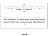
- FIG. 4 illustrates an example of a method 400 for driving a load using a low supply voltage in accordance with one or more implementations of the subject technology.
- the blocks of the example method 400 are described herein as occurring in serial, or linearly. However, multiple blocks of the example method 400 can occur in parallel. In addition, the blocks of the example method 400 need not be performed in the order shown and/or one or more of the blocks of the example method 400 need not be performed.
- the method 400 includes providing, by using a first circuit (e.g., 210 of FIG. 2A ), a desired termination impedance (e.g., R1+R4 or R3+R2 of FIG. 2B ) and a first portion of a desired output current to the load (e.g., R L of FIG. 2A ) (410).
- a second portion of the desired output current is provided, by using a second circuit (e.g., 220 of FIG. 2A ), such that the desired output current generates a predetermined voltage swing across the load, while the first circuit and the second circuit are powered by the low supply voltage (e.g., V DD of FIG. 2A ) (420).
- FIG. 5 illustrates an example of a communication device 500 employing features of the subject technology for driving one more loads using a low supply voltage in accordance with one or more implementations.
- the communication device 500 includes an Ethernet switch of an Ethernet network such as a private network including a data-center network, an enterprise network, or other private networks.
- the communication device 500 includes a number of ingress (input) ports IP1-IPn and multiple egress (output) ports EP1-EPm.
- one or more of the ingress ports IP1-IPn can receive a data packet from another switch or and endpoint device of the network.
- the communication device 500 further includes a hardware component such as an application specific integrated circuit (ASIC) 510 (which in some embodiments can be implemented as a field-programmable logic array (FPGA)), a buffer 520, a processor 530, memory 540, and a software module 550.
- ASIC application specific integrated circuit
- FPGA field-programmable logic array
- the ASIC 510 can include suitable logic, circuitry, interfaces and/or code that can be operable to perform functionalities of a PHY circuit.
- the buffer 520 includes suitable logic, circuitry, code and/or interfaces that are operable to receive and store and/or delay a block of data for communication through one or more of the egress ports EP1-EPm.
- the processor 530 includes suitable logic, circuitry, and/or code that can enable processing data and/or controlling operations of the communication device 500. In this regard, the processor 530 can be enabled to provide control signals to various other portions of the communication device 500.
- the processor 530 also controls transfers of data between various portions of the communication device 500. Additionally, the processor 530 can enable implementation of an operating system or otherwise execute code to manage operations of the communication device 500.
- the memory 540 includes suitable logic, circuitry, and/or code that can enable storage of various types of information such as received data, generated data, code, and/or configuration information.
- the memory 540 includes, for example, RAM, ROM, flash, and/or magnetic storage. In various embodiment of the subject technology, the memory 540 may include a RAM, DRAM, SRAM, T-RAM, Z-RAM, TTRAM, or any other storage media.
- the memory 540 can include software modules 550 that when executed by a processor (e.g., processor 530) can perform some or all of the functionalities of the ASIC 510.
- the software modules 550 include codes that when executed by a processor can perform functionalities such as configuration of the communication device 500.
- the communication device 500 may be implemented in a 28nm or smaller technology node and be powered by a low voltage supply (e.g., 0.8V).
- various chips e.g., the ASIC 510, the processor 530, and the memory 540
- the communication device 500 may be coupled to one another via lines that are driven by voltage-mode drivers of the subject technology such as the apparatuses shown in any of FIGs. 2A through 2E to provide acceptable voltage swings across input nodes of the chips.
- the communication device 500 includes one or more universal serial bus (USB) interfaces that can also be driven by the disclosed voltage-mode drivers and benefit from the advantages features of the subject technology such as low power consumption, reduced chip area, and without return loss.
- USB universal serial bus
- the phrase "at least one of” preceding a series of items, with the term “and” or “or” to separate any of the items, modifies the list as a whole, rather than each member of the list (i.e., each item).
- the phrase "at least one of” does not require selection of at least one of each item listed; rather, the phrase allows a meaning that includes at least one of any one of the items, and/or at least one of any combination of the items, and/or at least one of each of the items.
- phrases “at least one of A, B, and C” or “at least one of A, B, or C” each refer to only A, only B, or only C; any combination of A, B, and C; and/or at least one of each of A, B, and C.
- a phrase such as "an aspect” does not imply that such aspect is essential to the subject technology or that such aspect applies to all configurations of the subject technology.
- a disclosure relating to an aspect can apply to all configurations, or one or more configurations.
- An aspect can provide one or more examples of the disclosure.
- a phrase such as an "aspect” refers to one or more aspects and vice versa.
- a phrase such as an "embodiment” does not imply that such embodiment is essential to the subject technology or that such embodiment applies to all configurations of the subject technology.
- a disclosure relating to an embodiment can apply to all embodiments, or one or more embodiments.
- An embodiment can provide one or more examples of the disclosure.
- a phrase such an "embodiment” can refer to one or more embodiments and vice versa.
- a phrase such as a "configuration” does not imply that such configuration is essential to the subject technology or that such configuration applies to all configurations of the subject technology.
- a disclosure relating to a configuration can apply to all configurations, or one or more configurations.
- a configuration can provide one or more examples of the disclosure.
- a phrase such as a "configuration” can refer to one or more configurations and vice versa.
Landscapes
- Engineering & Computer Science (AREA)
- Power Engineering (AREA)
- Signal Processing (AREA)
- Computer Networks & Wireless Communication (AREA)
- Computer Hardware Design (AREA)
- General Engineering & Computer Science (AREA)
- Theoretical Computer Science (AREA)
- Physics & Mathematics (AREA)
- Mathematical Physics (AREA)
- Computing Systems (AREA)
- General Physics & Mathematics (AREA)
- Logic Circuits (AREA)
- Amplifiers (AREA)
- Dc-Dc Converters (AREA)
Applications Claiming Priority (2)
| Application Number | Priority Date | Filing Date | Title |
|---|---|---|---|
| US201462017176P | 2014-06-25 | 2014-06-25 | |
| US14/336,979 US10014846B2 (en) | 2014-06-25 | 2014-07-21 | Increasing output amplitude of a voltage-mode driver in a low supply voltage technology |
Publications (3)
| Publication Number | Publication Date |
|---|---|
| EP2961071A2 true EP2961071A2 (de) | 2015-12-30 |
| EP2961071A3 EP2961071A3 (de) | 2016-01-06 |
| EP2961071B1 EP2961071B1 (de) | 2022-12-14 |
Family
ID=53284023
Family Applications (1)
| Application Number | Title | Priority Date | Filing Date |
|---|---|---|---|
| EP15169217.5A Active EP2961071B1 (de) | 2014-06-25 | 2015-05-26 | Apparat und verfahren zum erhöhen der ausgangsamplitude eines spannungsmodustreibers in einer technologie mit niedriger versorgungsspannung |
Country Status (4)
| Country | Link |
|---|---|
| US (1) | US10014846B2 (de) |
| EP (1) | EP2961071B1 (de) |
| CN (1) | CN105279120B (de) |
| HK (1) | HK1215887A1 (de) |
Families Citing this family (4)
| Publication number | Priority date | Publication date | Assignee | Title |
|---|---|---|---|---|
| CN113315504A (zh) * | 2020-02-27 | 2021-08-27 | 成都纳能微电子有限公司 | Sst驱动结构 |
| TWI789197B (zh) * | 2022-01-03 | 2023-01-01 | 瑞昱半導體股份有限公司 | 乙太網路傳送端的輸出級 |
| EP4346110A1 (de) * | 2022-09-29 | 2024-04-03 | Nxp B.V. | Senderschaltung |
| US20240291488A1 (en) * | 2023-02-27 | 2024-08-29 | Stmicroelectronics International N.V. | Voltage compensation of differential voltage swing |
Family Cites Families (22)
| Publication number | Priority date | Publication date | Assignee | Title |
|---|---|---|---|---|
| US5629641A (en) * | 1996-02-06 | 1997-05-13 | Advanced Micro Devices, Inc. | Differential CMOS current amplifier with controlled bandwidth and common mode distortion |
| US5959490A (en) * | 1997-12-10 | 1999-09-28 | Pmc-Sierra Ltd. | High speed low voltage swing receiver for mixed supply voltage interfaces |
| US6121800A (en) * | 1998-07-07 | 2000-09-19 | Lucent Technologies, Inc. | Impedance matched, voltage-mode H-bridge write drivers |
| US6252450B1 (en) * | 1999-09-09 | 2001-06-26 | Stmicroelectronics, Inc. | Circuit and method for writing to a memory disk |
| US6704818B1 (en) | 2000-12-29 | 2004-03-09 | Intel Corporation | Voltage-mode driver with pre-emphasis, slew-rate control and source termination |
| US6686772B2 (en) | 2001-11-19 | 2004-02-03 | Broadcom Corporation | Voltage mode differential driver and method |
| US6812733B1 (en) * | 2002-08-02 | 2004-11-02 | Pmc-Sierra, Inc. | High-efficiency mixed voltage/current mode output driver |
| US7382190B2 (en) * | 2003-07-07 | 2008-06-03 | Analog Devices, Inc. | Variable attenuation system having continuous input steering |
| US6856178B1 (en) * | 2003-07-31 | 2005-02-15 | Silicon Bridge, Inc. | Multi-function input/output driver |
| US7323933B2 (en) * | 2005-04-07 | 2008-01-29 | Analog Devices, Inc. | Vector modulator having attenuators with continuous input steering |
| US7315186B2 (en) * | 2005-06-06 | 2008-01-01 | Intel Corporation | Voltage mode driver with current mode equalization |
| US7639746B2 (en) | 2005-07-01 | 2009-12-29 | Apple Inc. | Hybrid voltage/current-mode transmission line driver |
| US7224135B1 (en) * | 2006-09-07 | 2007-05-29 | Acutechnology Semiconductor Inc. | Imposed current motor drive |
| US7714615B2 (en) | 2007-12-28 | 2010-05-11 | Advanced Micro Devices, Inc. | De-emphasis circuit for a voltage mode driver used to communicate via a differential communication link |
| US7974589B2 (en) * | 2008-02-13 | 2011-07-05 | Analog Devices, Inc. | High-speed data transmitters |
| US8396106B2 (en) * | 2008-04-11 | 2013-03-12 | International Business Machines Corporation | System and method for improving equalization in a high speed serdes environment |
| WO2010111619A2 (en) * | 2009-03-27 | 2010-09-30 | Rambus, Inc. | Voltage mode transmitter equalizer |
| WO2013089773A1 (en) | 2011-12-16 | 2013-06-20 | Intel Corporation | Low voltage transmitter with variable output swing |
| US8520348B2 (en) * | 2011-12-22 | 2013-08-27 | Lsi Corporation | High-swing differential driver using low-voltage transistors |
| US8611437B2 (en) * | 2012-01-26 | 2013-12-17 | Nvidia Corporation | Ground referenced single-ended signaling |
| US8487654B1 (en) | 2012-02-29 | 2013-07-16 | Taiwan Semiconductor Manufacturing Co., Ltd. | Voltage mode driver with current booster (VMDCB) |
| US9312846B2 (en) * | 2013-07-16 | 2016-04-12 | Mediatek Inc. | Driver circuit for signal transmission and control method of driver circuit |
-
2014
- 2014-07-21 US US14/336,979 patent/US10014846B2/en active Active
-
2015
- 2015-05-26 EP EP15169217.5A patent/EP2961071B1/de active Active
- 2015-06-25 CN CN201510359484.3A patent/CN105279120B/zh active Active
-
2016
- 2016-04-05 HK HK16103793.5A patent/HK1215887A1/zh unknown
Non-Patent Citations (1)
| Title |
|---|
| None |
Also Published As
| Publication number | Publication date |
|---|---|
| HK1215887A1 (zh) | 2016-09-23 |
| CN105279120A (zh) | 2016-01-27 |
| EP2961071A3 (de) | 2016-01-06 |
| CN105279120B (zh) | 2019-06-21 |
| US10014846B2 (en) | 2018-07-03 |
| US20150381150A1 (en) | 2015-12-31 |
| EP2961071B1 (de) | 2022-12-14 |
Similar Documents
| Publication | Publication Date | Title |
|---|---|---|
| TWI740114B (zh) | 具有自低電力待機至低頻信號傳輸之快速變換之轉發器 | |
| US9413381B2 (en) | High-speed, low-power reconfigurable voltage-mode DAC-driver | |
| US9984033B2 (en) | Systems and methods for biasing a bus | |
| EP3758229B1 (de) | Vorrichtungen und verfahren mit einem segmentierten quellenreihenterminierten leitungstreiber | |
| US7808277B2 (en) | Bidirectional signal separation module for a bus converter | |
| US11483184B2 (en) | Multi pulse amplitude modulation signaling decision feedback equalizer having power differentiating modes and tap-weight re-configuration | |
| KR20140053241A (ko) | 전하 주입을 포함한 차동 직렬 신호들을 전달하는 장치들 및 방법들 | |
| TW201931139A (zh) | 用於功率效率驅動電路之裝置與方法 | |
| EP2961071A2 (de) | Erhöhen der ausgangsamplitude eines spannungsmodustreibers in einer technologie mit niedriger versorgungsspannung | |
| EP2118760B1 (de) | Bidirektionale schnittstellenschaltung mit einem umschaltbaren stromquellen-bias | |
| US9325316B1 (en) | Low-power high swing CML driver with independent common-mode and swing control | |
| CN111800355A (zh) | 传输器、成像系统以及通信系统 | |
| US8222925B2 (en) | Multimode Ethernet line driver | |
| US10135643B1 (en) | Decision feedback equalizer with distributed R-C network | |
| CN109417521B (zh) | 低功率多电平驱动器 | |
| US6968413B2 (en) | Method and system for configuring terminators in a serial communication system | |
| US20230075962A1 (en) | Termination for Pulse Amplitude Modulation | |
| US9215104B1 (en) | Floating taps for decision feedback equalizer | |
| US8755474B2 (en) | Signal conditioning by combining precursor, main, and post cursor signals without a clock signal | |
| KR101995027B1 (ko) | 정전류 소모가 없는 저전력 송신기 | |
| JP5626240B2 (ja) | ドライバ回路 | |
| KR102034221B1 (ko) | 클록 신호 발생부를 포함하는 반도체 장치 | |
| US20160043719A1 (en) | High voltage fail-safe io design using thin oxide devices | |
| KR102740335B1 (ko) | 메모리 인터페이스를 위한 PAM-3 드라이버의 ZQ Calibration 장치 및 방법 | |
| KR102823144B1 (ko) | Pam-3 신호처리용 미들전압 터미네이션 기반 드라이버 장치 |
Legal Events
| Date | Code | Title | Description |
|---|---|---|---|
| PUAL | Search report despatched |
Free format text: ORIGINAL CODE: 0009013 |
|
| PUAI | Public reference made under article 153(3) epc to a published international application that has entered the european phase |
Free format text: ORIGINAL CODE: 0009012 |
|
| AK | Designated contracting states |
Kind code of ref document: A2 Designated state(s): AL AT BE BG CH CY CZ DE DK EE ES FI FR GB GR HR HU IE IS IT LI LT LU LV MC MK MT NL NO PL PT RO RS SE SI SK SM TR |
|
| AX | Request for extension of the european patent |
Extension state: BA ME |
|
| AK | Designated contracting states |
Kind code of ref document: A3 Designated state(s): AL AT BE BG CH CY CZ DE DK EE ES FI FR GB GR HR HU IE IS IT LI LT LU LV MC MK MT NL NO PL PT RO RS SE SI SK SM TR |
|
| AX | Request for extension of the european patent |
Extension state: BA ME |
|
| RIC1 | Information provided on ipc code assigned before grant |
Ipc: H03K 19/0175 20060101AFI20151201BHEP Ipc: H04L 25/02 20060101ALI20151201BHEP |
|
| 17P | Request for examination filed |
Effective date: 20160706 |
|
| RBV | Designated contracting states (corrected) |
Designated state(s): AL AT BE BG CH CY CZ DE DK EE ES FI FR GB GR HR HU IE IS IT LI LT LU LV MC MK MT NL NO PL PT RO RS SE SI SK SM TR |
|
| RAP1 | Party data changed (applicant data changed or rights of an application transferred) |
Owner name: AVAGO TECHNOLOGIES GENERAL IP (SINGAPORE) PTE. LTD |
|
| RAP1 | Party data changed (applicant data changed or rights of an application transferred) |
Owner name: AVAGO TECHNOLOGIES INTERNATIONAL SALES PTE. LIMITE |
|
| STAA | Information on the status of an ep patent application or granted ep patent |
Free format text: STATUS: EXAMINATION IS IN PROGRESS |
|
| 17Q | First examination report despatched |
Effective date: 20190509 |
|
| GRAP | Despatch of communication of intention to grant a patent |
Free format text: ORIGINAL CODE: EPIDOSNIGR1 |
|
| STAA | Information on the status of an ep patent application or granted ep patent |
Free format text: STATUS: GRANT OF PATENT IS INTENDED |
|
| INTG | Intention to grant announced |
Effective date: 20220622 |
|
| GRAS | Grant fee paid |
Free format text: ORIGINAL CODE: EPIDOSNIGR3 |
|
| GRAA | (expected) grant |
Free format text: ORIGINAL CODE: 0009210 |
|
| STAA | Information on the status of an ep patent application or granted ep patent |
Free format text: STATUS: THE PATENT HAS BEEN GRANTED |
|
| AK | Designated contracting states |
Kind code of ref document: B1 Designated state(s): AL AT BE BG CH CY CZ DE DK EE ES FI FR GB GR HR HU IE IS IT LI LT LU LV MC MK MT NL NO PL PT RO RS SE SI SK SM TR |
|
| REG | Reference to a national code |
Ref country code: GB Ref legal event code: FG4D |
|
| REG | Reference to a national code |
Ref country code: CH Ref legal event code: EP |
|
| REG | Reference to a national code |
Ref country code: DE Ref legal event code: R096 Ref document number: 602015081928 Country of ref document: DE |
|
| REG | Reference to a national code |
Ref country code: IE Ref legal event code: FG4D |
|
| REG | Reference to a national code |
Ref country code: AT Ref legal event code: REF Ref document number: 1538282 Country of ref document: AT Kind code of ref document: T Effective date: 20230115 |
|
| REG | Reference to a national code |
Ref country code: NL Ref legal event code: FP |
|
| REG | Reference to a national code |
Ref country code: LT Ref legal event code: MG9D |
|
| PG25 | Lapsed in a contracting state [announced via postgrant information from national office to epo] |
Ref country code: SE Free format text: LAPSE BECAUSE OF FAILURE TO SUBMIT A TRANSLATION OF THE DESCRIPTION OR TO PAY THE FEE WITHIN THE PRESCRIBED TIME-LIMIT Effective date: 20221214 Ref country code: NO Free format text: LAPSE BECAUSE OF FAILURE TO SUBMIT A TRANSLATION OF THE DESCRIPTION OR TO PAY THE FEE WITHIN THE PRESCRIBED TIME-LIMIT Effective date: 20230314 Ref country code: LT Free format text: LAPSE BECAUSE OF FAILURE TO SUBMIT A TRANSLATION OF THE DESCRIPTION OR TO PAY THE FEE WITHIN THE PRESCRIBED TIME-LIMIT Effective date: 20221214 Ref country code: FI Free format text: LAPSE BECAUSE OF FAILURE TO SUBMIT A TRANSLATION OF THE DESCRIPTION OR TO PAY THE FEE WITHIN THE PRESCRIBED TIME-LIMIT Effective date: 20221214 |
|
| REG | Reference to a national code |
Ref country code: AT Ref legal event code: MK05 Ref document number: 1538282 Country of ref document: AT Kind code of ref document: T Effective date: 20221214 |
|
| PG25 | Lapsed in a contracting state [announced via postgrant information from national office to epo] |
Ref country code: RS Free format text: LAPSE BECAUSE OF FAILURE TO SUBMIT A TRANSLATION OF THE DESCRIPTION OR TO PAY THE FEE WITHIN THE PRESCRIBED TIME-LIMIT Effective date: 20221214 Ref country code: LV Free format text: LAPSE BECAUSE OF FAILURE TO SUBMIT A TRANSLATION OF THE DESCRIPTION OR TO PAY THE FEE WITHIN THE PRESCRIBED TIME-LIMIT Effective date: 20221214 Ref country code: HR Free format text: LAPSE BECAUSE OF FAILURE TO SUBMIT A TRANSLATION OF THE DESCRIPTION OR TO PAY THE FEE WITHIN THE PRESCRIBED TIME-LIMIT Effective date: 20221214 Ref country code: GR Free format text: LAPSE BECAUSE OF FAILURE TO SUBMIT A TRANSLATION OF THE DESCRIPTION OR TO PAY THE FEE WITHIN THE PRESCRIBED TIME-LIMIT Effective date: 20230315 |
|
| PG25 | Lapsed in a contracting state [announced via postgrant information from national office to epo] |
Ref country code: SM Free format text: LAPSE BECAUSE OF FAILURE TO SUBMIT A TRANSLATION OF THE DESCRIPTION OR TO PAY THE FEE WITHIN THE PRESCRIBED TIME-LIMIT Effective date: 20221214 Ref country code: RO Free format text: LAPSE BECAUSE OF FAILURE TO SUBMIT A TRANSLATION OF THE DESCRIPTION OR TO PAY THE FEE WITHIN THE PRESCRIBED TIME-LIMIT Effective date: 20221214 Ref country code: PT Free format text: LAPSE BECAUSE OF FAILURE TO SUBMIT A TRANSLATION OF THE DESCRIPTION OR TO PAY THE FEE WITHIN THE PRESCRIBED TIME-LIMIT Effective date: 20230414 Ref country code: ES Free format text: LAPSE BECAUSE OF FAILURE TO SUBMIT A TRANSLATION OF THE DESCRIPTION OR TO PAY THE FEE WITHIN THE PRESCRIBED TIME-LIMIT Effective date: 20221214 Ref country code: EE Free format text: LAPSE BECAUSE OF FAILURE TO SUBMIT A TRANSLATION OF THE DESCRIPTION OR TO PAY THE FEE WITHIN THE PRESCRIBED TIME-LIMIT Effective date: 20221214 Ref country code: CZ Free format text: LAPSE BECAUSE OF FAILURE TO SUBMIT A TRANSLATION OF THE DESCRIPTION OR TO PAY THE FEE WITHIN THE PRESCRIBED TIME-LIMIT Effective date: 20221214 Ref country code: AT Free format text: LAPSE BECAUSE OF FAILURE TO SUBMIT A TRANSLATION OF THE DESCRIPTION OR TO PAY THE FEE WITHIN THE PRESCRIBED TIME-LIMIT Effective date: 20221214 |
|
| PG25 | Lapsed in a contracting state [announced via postgrant information from national office to epo] |
Ref country code: SK Free format text: LAPSE BECAUSE OF FAILURE TO SUBMIT A TRANSLATION OF THE DESCRIPTION OR TO PAY THE FEE WITHIN THE PRESCRIBED TIME-LIMIT Effective date: 20221214 Ref country code: PL Free format text: LAPSE BECAUSE OF FAILURE TO SUBMIT A TRANSLATION OF THE DESCRIPTION OR TO PAY THE FEE WITHIN THE PRESCRIBED TIME-LIMIT Effective date: 20221214 Ref country code: IS Free format text: LAPSE BECAUSE OF FAILURE TO SUBMIT A TRANSLATION OF THE DESCRIPTION OR TO PAY THE FEE WITHIN THE PRESCRIBED TIME-LIMIT Effective date: 20230414 Ref country code: AL Free format text: LAPSE BECAUSE OF FAILURE TO SUBMIT A TRANSLATION OF THE DESCRIPTION OR TO PAY THE FEE WITHIN THE PRESCRIBED TIME-LIMIT Effective date: 20221214 |
|
| REG | Reference to a national code |
Ref country code: DE Ref legal event code: R097 Ref document number: 602015081928 Country of ref document: DE |
|
| PLBE | No opposition filed within time limit |
Free format text: ORIGINAL CODE: 0009261 |
|
| STAA | Information on the status of an ep patent application or granted ep patent |
Free format text: STATUS: NO OPPOSITION FILED WITHIN TIME LIMIT |
|
| PG25 | Lapsed in a contracting state [announced via postgrant information from national office to epo] |
Ref country code: DK Free format text: LAPSE BECAUSE OF FAILURE TO SUBMIT A TRANSLATION OF THE DESCRIPTION OR TO PAY THE FEE WITHIN THE PRESCRIBED TIME-LIMIT Effective date: 20221214 |
|
| 26N | No opposition filed |
Effective date: 20230915 |
|
| PG25 | Lapsed in a contracting state [announced via postgrant information from national office to epo] |
Ref country code: SI Free format text: LAPSE BECAUSE OF FAILURE TO SUBMIT A TRANSLATION OF THE DESCRIPTION OR TO PAY THE FEE WITHIN THE PRESCRIBED TIME-LIMIT Effective date: 20221214 |
|
| REG | Reference to a national code |
Ref country code: CH Ref legal event code: PL |
|
| PG25 | Lapsed in a contracting state [announced via postgrant information from national office to epo] |
Ref country code: MC Free format text: LAPSE BECAUSE OF FAILURE TO SUBMIT A TRANSLATION OF THE DESCRIPTION OR TO PAY THE FEE WITHIN THE PRESCRIBED TIME-LIMIT Effective date: 20221214 |
|
| GBPC | Gb: european patent ceased through non-payment of renewal fee |
Effective date: 20230526 |
|
| REG | Reference to a national code |
Ref country code: BE Ref legal event code: MM Effective date: 20230531 |
|
| PG25 | Lapsed in a contracting state [announced via postgrant information from national office to epo] |
Ref country code: MC Free format text: LAPSE BECAUSE OF FAILURE TO SUBMIT A TRANSLATION OF THE DESCRIPTION OR TO PAY THE FEE WITHIN THE PRESCRIBED TIME-LIMIT Effective date: 20221214 Ref country code: LU Free format text: LAPSE BECAUSE OF NON-PAYMENT OF DUE FEES Effective date: 20230526 Ref country code: LI Free format text: LAPSE BECAUSE OF NON-PAYMENT OF DUE FEES Effective date: 20230531 Ref country code: CH Free format text: LAPSE BECAUSE OF NON-PAYMENT OF DUE FEES Effective date: 20230531 |
|
| REG | Reference to a national code |
Ref country code: IE Ref legal event code: MM4A |
|
| PG25 | Lapsed in a contracting state [announced via postgrant information from national office to epo] |
Ref country code: IE Free format text: LAPSE BECAUSE OF NON-PAYMENT OF DUE FEES Effective date: 20230526 |
|
| PG25 | Lapsed in a contracting state [announced via postgrant information from national office to epo] |
Ref country code: IE Free format text: LAPSE BECAUSE OF NON-PAYMENT OF DUE FEES Effective date: 20230526 Ref country code: GB Free format text: LAPSE BECAUSE OF NON-PAYMENT OF DUE FEES Effective date: 20230526 |
|
| PG25 | Lapsed in a contracting state [announced via postgrant information from national office to epo] |
Ref country code: IT Free format text: LAPSE BECAUSE OF FAILURE TO SUBMIT A TRANSLATION OF THE DESCRIPTION OR TO PAY THE FEE WITHIN THE PRESCRIBED TIME-LIMIT Effective date: 20221214 Ref country code: BE Free format text: LAPSE BECAUSE OF NON-PAYMENT OF DUE FEES Effective date: 20230531 |
|
| PG25 | Lapsed in a contracting state [announced via postgrant information from national office to epo] |
Ref country code: BG Free format text: LAPSE BECAUSE OF FAILURE TO SUBMIT A TRANSLATION OF THE DESCRIPTION OR TO PAY THE FEE WITHIN THE PRESCRIBED TIME-LIMIT Effective date: 20221214 |
|
| PG25 | Lapsed in a contracting state [announced via postgrant information from national office to epo] |
Ref country code: BG Free format text: LAPSE BECAUSE OF FAILURE TO SUBMIT A TRANSLATION OF THE DESCRIPTION OR TO PAY THE FEE WITHIN THE PRESCRIBED TIME-LIMIT Effective date: 20221214 |
|
| PGFP | Annual fee paid to national office [announced via postgrant information from national office to epo] |
Ref country code: NL Payment date: 20250423 Year of fee payment: 11 |
|
| PGFP | Annual fee paid to national office [announced via postgrant information from national office to epo] |
Ref country code: DE Payment date: 20250423 Year of fee payment: 11 |
|
| PGFP | Annual fee paid to national office [announced via postgrant information from national office to epo] |
Ref country code: FR Payment date: 20250423 Year of fee payment: 11 |
|
| PG25 | Lapsed in a contracting state [announced via postgrant information from national office to epo] |
Ref country code: CY Free format text: LAPSE BECAUSE OF FAILURE TO SUBMIT A TRANSLATION OF THE DESCRIPTION OR TO PAY THE FEE WITHIN THE PRESCRIBED TIME-LIMIT; INVALID AB INITIO Effective date: 20150526 |
|
| PG25 | Lapsed in a contracting state [announced via postgrant information from national office to epo] |
Ref country code: HU Free format text: LAPSE BECAUSE OF FAILURE TO SUBMIT A TRANSLATION OF THE DESCRIPTION OR TO PAY THE FEE WITHIN THE PRESCRIBED TIME-LIMIT; INVALID AB INITIO Effective date: 20150526 |
|
| PG25 | Lapsed in a contracting state [announced via postgrant information from national office to epo] |
Ref country code: TR Free format text: LAPSE BECAUSE OF FAILURE TO SUBMIT A TRANSLATION OF THE DESCRIPTION OR TO PAY THE FEE WITHIN THE PRESCRIBED TIME-LIMIT Effective date: 20221214 |