EP2961069A1 - Electric machine system and igbt switch circuit thereof - Google Patents
Electric machine system and igbt switch circuit thereof Download PDFInfo
- Publication number
- EP2961069A1 EP2961069A1 EP15173987.7A EP15173987A EP2961069A1 EP 2961069 A1 EP2961069 A1 EP 2961069A1 EP 15173987 A EP15173987 A EP 15173987A EP 2961069 A1 EP2961069 A1 EP 2961069A1
- Authority
- EP
- European Patent Office
- Prior art keywords
- circuit
- igbt
- switch
- electric machine
- bipolar junction
- Prior art date
- Legal status (The legal status is an assumption and is not a legal conclusion. Google has not performed a legal analysis and makes no representation as to the accuracy of the status listed.)
- Granted
Links
Images


Classifications
-
- H—ELECTRICITY
- H03—ELECTRONIC CIRCUITRY
- H03K—PULSE TECHNIQUE
- H03K17/00—Electronic switching or gating, i.e. not by contact-making and –breaking
- H03K17/16—Modifications for eliminating interference voltages or currents
- H03K17/168—Modifications for eliminating interference voltages or currents in composite switches
-
- H—ELECTRICITY
- H02—GENERATION; CONVERSION OR DISTRIBUTION OF ELECTRIC POWER
- H02M—APPARATUS FOR CONVERSION BETWEEN AC AND AC, BETWEEN AC AND DC, OR BETWEEN DC AND DC, AND FOR USE WITH MAINS OR SIMILAR POWER SUPPLY SYSTEMS; CONVERSION OF DC OR AC INPUT POWER INTO SURGE OUTPUT POWER; CONTROL OR REGULATION THEREOF
- H02M1/00—Details of apparatus for conversion
- H02M1/08—Circuits specially adapted for the generation of control voltages for semiconductor devices incorporated in static converters
-
- H—ELECTRICITY
- H02—GENERATION; CONVERSION OR DISTRIBUTION OF ELECTRIC POWER
- H02M—APPARATUS FOR CONVERSION BETWEEN AC AND AC, BETWEEN AC AND DC, OR BETWEEN DC AND DC, AND FOR USE WITH MAINS OR SIMILAR POWER SUPPLY SYSTEMS; CONVERSION OF DC OR AC INPUT POWER INTO SURGE OUTPUT POWER; CONTROL OR REGULATION THEREOF
- H02M1/00—Details of apparatus for conversion
- H02M1/32—Means for protecting converters other than automatic disconnection
- H02M1/34—Snubber circuits
- H02M1/342—Active non-dissipative snubbers
-
- H—ELECTRICITY
- H02—GENERATION; CONVERSION OR DISTRIBUTION OF ELECTRIC POWER
- H02M—APPARATUS FOR CONVERSION BETWEEN AC AND AC, BETWEEN AC AND DC, OR BETWEEN DC AND DC, AND FOR USE WITH MAINS OR SIMILAR POWER SUPPLY SYSTEMS; CONVERSION OF DC OR AC INPUT POWER INTO SURGE OUTPUT POWER; CONTROL OR REGULATION THEREOF
- H02M7/00—Conversion of AC power input into DC power output; Conversion of DC power input into AC power output
- H02M7/42—Conversion of DC power input into AC power output without possibility of reversal
- H02M7/44—Conversion of DC power input into AC power output without possibility of reversal by static converters
- H02M7/48—Conversion of DC power input into AC power output without possibility of reversal by static converters using discharge tubes with control electrode or semiconductor devices with control electrode
- H02M7/53—Conversion of DC power input into AC power output without possibility of reversal by static converters using discharge tubes with control electrode or semiconductor devices with control electrode using devices of a triode or transistor type requiring continuous application of a control signal
- H02M7/537—Conversion of DC power input into AC power output without possibility of reversal by static converters using discharge tubes with control electrode or semiconductor devices with control electrode using devices of a triode or transistor type requiring continuous application of a control signal using semiconductor devices only, e.g. single switched pulse inverters
- H02M7/5387—Conversion of DC power input into AC power output without possibility of reversal by static converters using discharge tubes with control electrode or semiconductor devices with control electrode using devices of a triode or transistor type requiring continuous application of a control signal using semiconductor devices only, e.g. single switched pulse inverters in a bridge configuration
-
- H—ELECTRICITY
- H02—GENERATION; CONVERSION OR DISTRIBUTION OF ELECTRIC POWER
- H02M—APPARATUS FOR CONVERSION BETWEEN AC AND AC, BETWEEN AC AND DC, OR BETWEEN DC AND DC, AND FOR USE WITH MAINS OR SIMILAR POWER SUPPLY SYSTEMS; CONVERSION OF DC OR AC INPUT POWER INTO SURGE OUTPUT POWER; CONTROL OR REGULATION THEREOF
- H02M7/00—Conversion of AC power input into DC power output; Conversion of DC power input into AC power output
- H02M7/66—Conversion of AC power input into DC power output; Conversion of DC power input into AC power output with possibility of reversal
- H02M7/68—Conversion of AC power input into DC power output; Conversion of DC power input into AC power output with possibility of reversal by static converters
- H02M7/72—Conversion of AC power input into DC power output; Conversion of DC power input into AC power output with possibility of reversal by static converters using discharge tubes with control electrode or semiconductor devices with control electrode
- H02M7/79—Conversion of AC power input into DC power output; Conversion of DC power input into AC power output with possibility of reversal by static converters using discharge tubes with control electrode or semiconductor devices with control electrode using devices of a triode or transistor type requiring continuous application of a control signal
- H02M7/797—Conversion of AC power input into DC power output; Conversion of DC power input into AC power output with possibility of reversal by static converters using discharge tubes with control electrode or semiconductor devices with control electrode using devices of a triode or transistor type requiring continuous application of a control signal using semiconductor devices only
-
- H—ELECTRICITY
- H03—ELECTRONIC CIRCUITRY
- H03K—PULSE TECHNIQUE
- H03K17/00—Electronic switching or gating, i.e. not by contact-making and –breaking
- H03K17/08—Modifications for protecting switching circuit against overcurrent or overvoltage
- H03K17/082—Modifications for protecting switching circuit against overcurrent or overvoltage by feedback from the output to the control circuit
- H03K17/0828—Modifications for protecting switching circuit against overcurrent or overvoltage by feedback from the output to the control circuit in composite switches
-
- Y—GENERAL TAGGING OF NEW TECHNOLOGICAL DEVELOPMENTS; GENERAL TAGGING OF CROSS-SECTIONAL TECHNOLOGIES SPANNING OVER SEVERAL SECTIONS OF THE IPC; TECHNICAL SUBJECTS COVERED BY FORMER USPC CROSS-REFERENCE ART COLLECTIONS [XRACs] AND DIGESTS
- Y02—TECHNOLOGIES OR APPLICATIONS FOR MITIGATION OR ADAPTATION AGAINST CLIMATE CHANGE
- Y02B—CLIMATE CHANGE MITIGATION TECHNOLOGIES RELATED TO BUILDINGS, e.g. HOUSING, HOUSE APPLIANCES OR RELATED END-USER APPLICATIONS
- Y02B70/00—Technologies for an efficient end-user side electric power management and consumption
- Y02B70/10—Technologies improving the efficiency by using switched-mode power supplies [SMPS], i.e. efficient power electronics conversion e.g. power factor correction or reduction of losses in power supplies or efficient standby modes
Definitions
- the present invention relates to the field of electrically driven motor vehicles, in particular to an electric machine system for an electrically driven motor vehicle and an IGBT switch circuit thereof.
- An electrically driven motor vehicle is a new type of vehicle, in which a vehicle-mounted power supply provides motive power, and the wheels are driven to travel by an electric machine. Compared with conventional motor vehicles, electrically driven motor vehicles have very little effect on the environment, and for this reason are widely regarded as having favorable prospects.
- hybrid motor vehicles on the market in which an electrically driven motor vehicle is combined with a conventional motor vehicle.
- Such a vehicle is fitted with two or more motive power source systems, e.g. a hybrid motor vehicle with an internal combustion engine vehicle generator and a storage battery.
- an IGBT Insulated Gate Bipolar Transistor
- an IGBT circuit may be regarded as a high-frequency modulating switch between the electric machine system and the motor vehicle for adjusting duty cycle.
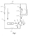
- Fig. 1 shows a structural schematic diagram of an IGBT circuit according to the prior art. As Fig. 1 shows, the IGBT circuit is formed by the combination of a bipolar junction transistor T 1 and a diode d 1 connected in parallel. When the IGBT needs to switch off, i.e.
- the input voltage i.e. the voltage between the gate and emitter of the bipolar junction transistor T 1
- V ge in the IGBT circuit will suddenly decrease. Due to connecting lines/connecting elements in the system, parasitic inductance will arise in each circuit branch, e.g. parasitic inductance ls 11 , parasitic inductance ls 12 , parasitic inductance ls 14 and parasitic inductance ls 13 , as shown in Fig. 1 .
- V induced voltage L parasitic inductance • ⁇ ⁇ I c
- L parasitic inductance is the equivalent value of parasitic inductance of the parasitic inductance ls 11 , parasitic inductance ls 12 , parasitic inductance ls 14 and parasitic inductance ls 13 of the branches.
- the output voltage V ce of the bipolar junction transistor T 1 (i.e. the voltage between the emitter and collector of the bipolar junction transistor T 1 ) will experience a spike.
- Fig. 2 (a) is a graph of output voltage of an IGBT circuit according to the prior art, wherein the horizontal coordinates represent time, and the vertical coordinates represent the output voltage V ce of the IGBT circuit, i.e. the voltage between the emitter and collector of the bipolar junction transistor T 1 .
- Fig. 2(b) is a graph of input voltage of an IGBT circuit in the prior art, wherein the horizontal coordinates represent time, and the vertical coordinates represent the input voltage of the IGBT circuit, i.e. the voltage V ge between the gate and emitter of the bipolar junction transistor T 1 .
- I c is the input current of the bipolar junction transistor T 1 , i.e. the current which flows in from the collector of the bipolar junction transistor T 1 .
- the time axis of Fig. 2(a) corresponds to the time axis of Fig. 2(b) .
- V dc the bus voltage, i.e. the total voltage of the system.
- V tr represents the spike voltage of the bipolar junction transistor T 1 .
- the electric machine system 200 begins to disconnect the supply of electric power with the electrically driven motor vehicle 100, and the input voltage V ge at the bipolar junction transistor T 1 decreases, i.e. the input current I c of the bipolar junction transistor T 1 begins to decrease.
- V tr reaches a very high value, so that Vce overvoltage damages the IGBT circuit.
- a protection circuit will generally be provided for the IGBT circuit, but the provision of a protection circuit will give rise to new problems.
- the present invention proposes an electric machine system and an IGBT switch circuit thereof.
- One aspect of the present invention provides an IGBT switch circuit, wherein the IGBT switch circuit comprises: an IGBT circuit and a first diode, the IGBT circuit serving as a modulating switch between an electric machine and a load thereof; an active clamping protection circuit coupled to the IGBT circuit; with a switch also being connected between the IGBT circuit and the protection circuit.
- the solution can solve the problem of damage to the IGBT caused by overvoltage at the output of the bipolar junction transistor in the IGBT when the IGBT is switched off.
- the solution can also solve the technical problem whereby, when the electric machine is back-dragged to a maximum speed, the electric machine becomes a generator and produces very high reverse potential, increasing the bus voltage to an overvoltage state, and finally causing the voltage across the collector and emitter of the IGBT to reach an opening voltage of the active clamping circuit serving as the protection circuit, possibly causing the IGBT to be switched on erroneously or the active clamping circuit to be damaged.
- the bipolar junction transistor is an NPN bipolar junction transistor.
- the protection circuit comprises a transient suppression diode and a second diode connected in series.
- the protection circuit uses the reverse breakdown characteristic of the transient suppression diode, for clamping the point potential.
- the switch comprises a PMOS, with a source thereof connected to the second diode of the protection circuit, and a drain thereof connected to a gate of the bipolar junction transistor of the IGBT circuit.
- the present invention uses the period characteristic of the PMOS, to realize a switch function.
- the switch is also connected to an NMOS, with a drain thereof coupled to a gate of the PMOS serving as the switch, and a source thereof connected to ground. Since a control signal cannot be transmitted directly to the switch, a buffer function for level matching must be served.
- the IGBT switch circuit also comprises a gate level driver connected to a gate of the NMOS, for driving the IGBT circuit.
- a resistance circuit is also connected between the gate level driver and the gate of the NMOS, for controlling the drive speed of the IGBT circuit.
- the switch circuit also comprises a control circuit, which issues a control signal to control the opening and closing of the switch.
- control signal is a square wave signal of a specific frequency, which controls the switch to remain closed when the electricity supply of the electric machine and the load thereof is disconnected.
- the switch When the IGBT circuit is switched on, the switch is controlled to conduct electricity, and the protection circuit operates normally.
- a first IGBT circuit When a first IGBT circuit is switched off, the switch maintains a closed state (is at a HIGH level) for a period of time, to ensure that the protection circuit operates normally in order to effectively suppress a spike value, then the switch turns off, so that the IGBT circuit is not erroneously switched on and thereby damaged by a reverse potential overvoltage.
- a second aspect of the present invention provides an electric machine system, wherein the electric machine system comprises an electric machine for driving a load, wherein at least three branches are included, each branch being connected to two parallel-connected IGBT switch circuits according to the first aspect of the present invention.
- a third aspect of the present invention provides an electrically driven motor vehicle, wherein it comprises an electric machine system according to the second aspect of the present invention.
- the following description takes as an example the application of the electric machine system and IGBT switch circuit thereof to the field of electrically driven motor vehicles, wherein the electric machine system is used to provide electric power for the tires of an electrically driven motor vehicle, so that the tires of the electrically driven motor vehicle acquire motive power to drive the motor vehicle to travel, and the IGBT switch circuit is used to drive the electric machine system to provide electric power for the tires of the electrically driven motor vehicle.
- the electric machine system is used to provide electric power for the tires of an electrically driven motor vehicle, so that the tires of the electrically driven motor vehicle acquire motive power to drive the motor vehicle to travel
- the IGBT switch circuit is used to drive the electric machine system to provide electric power for the tires of the electrically driven motor vehicle.
- FIG. 3 is a schematic diagram of the modular structure of an electric machine system according to a particular embodiment of the present invention.
- an electric machine 200 supplies electricity to an electrically driven motor vehicle 100 by means of torque control, so that the electrically driven motor vehicle 100 converts electric power to motive power for the rotation of the wheels.
- An IGBT circuit serves as a switch between the electric machine 200 and the electrically driven motor vehicle 100; according to a preferred embodiment of the present invention, the IGBT circuit comprises a first IGBT circuit 2011, a second IGBT circuit 2012, a third IGBT circuit 2013, a fourth IGBT circuit 2014, a fifth IGBT circuit 2015 and a sixth IGBT circuit 2016. It must be explained that the number of IGBT circuits is determined according to the electric machine 200; a detailed explanation is given below.
- a circuit downstream of the IGBT circuit is provided with a switch S 2 , which is driven by a control signal PWM sent by a control circuit C 2 .
- the IGBT circuit is also connected to a protection circuit P, used to protect the IGBT circuit from the effects of overvoltage.
- Fig. 4 is a schematic diagram of the connection between the electric machine system and IGBT switch circuit according to a particular embodiment of the present invention.
- Electric machines in common use in the industry at the moment generally have three branches, as Fig. 4 shows; according to a particular embodiment of the present invention, the electric machine M has three branches, namely a first branch A, a second branch B and a third branch C. Since a bus voltage Udc provided by a system power supply has two directions (positive and negative), the first branch A, second branch B and third branch C each require two IGBT circuits. Specifically, as Fig.
- the first branch A is connected to the first IGBT circuit 2011 and second IGBT gate level 2012 which are connected in parallel, wherein the first IGBT circuit 2011 is connected to a positive pole of the bus voltage, and the second IGBT circuit 2012 is connected to a negative pole of the bus voltage;
- the second branch B is connected to the third IGBT circuit 2013 and fourth IGBT gate level 2014 which are connected in parallel, wherein the third IGBT circuit 2013 is connected to the positive pole of the bus voltage, and the fourth IGBT circuit 2014 is connected to the negative pole of the bus voltage;
- the third branch C is connected to the fifth IGBT circuit 2015 and sixth IGBT circuit 2016 which are connected in parallel, wherein the fifth IGBT circuit 2015 is connected to the positive pole of the bus voltage, and the sixth IGBT circuit 2016 is connected to the negative pole of the bus voltage.
- the present invention is explained below, taking the IGBT switch circuit connected to the first branch A in the electric machine shown in Fig. 4 as an example.
- Fig. 5 is a circuit connection diagram of an IGBT circuit and a protection circuit thereof according to a particular embodiment of the present invention.
- the inductance L in Fig. 5 is equivalent to an inductance L in the electric machine 200 in Fig. 4 ;
- the IGBT circuit shown in Fig. 5 is equivalent to one of the IGBT circuits connected in parallel with the first branch A in Fig. 5 , e.g. the first IGBT circuit 2011.
- a first aspect of the present invention provides an IGBT switch circuit, wherein the IGBT switch circuit comprises a first IGBT circuit 2011, which consists of an NPN bipolar junction transistor T 21 and a first diode d 21 connected in parallel; the first IGBT circuit 2011 serves as a high-frequency modulating switch between the electric machine system and the motor vehicle for adjusting duty cycle.
- the load is an electrically driven motor vehicle by way of example.
- the IGBT switch circuit provided by the present invention is also specially provided with a protection circuit P for the first IGBT circuit 2011;
- the protection circuit P is an active clamping circuit, comprising a transient suppression diode TVS and a second diode d 22 , which are reverse-connected in series.
- the transient suppression diode is also called a clamping diode, and is a highly efficient circuit protection device that is widely used in the industry at present, which can absorb power surges up to several kilowatts.
- the main characteristic of the transient suppression diode TVS is that it experiences reverse breakdown and begins conducting as soon as a reverse voltage exceeds a rated value, thereby allowing the passage of a large current while clamping the voltage at a preset level.
- the input voltage V ge of the bipolar junction transistor T 21 in the first IGBT circuit 2011 falls when the electrical connection between the electric machine and the electrically driven motor vehicle is broken, the input current I c thereof also falls; at this point, the parasitic inductance Ls 21 , parasitic inductance Ls 22 , parasitic inductance Ls 23 and parasitic inductance Ls 24 give rise to an induced voltage due to a change in the change rate of the input current I c ; the induced voltage acts on the bipolar junction transistor T 21 in the first IGBT circuit 2011, causing a very large value (spike value) in the output voltage of the bipolar junction transistor T 21 and thereby damaging the IGBT circuit.
- the protection circuit P is provided precisely in order to solve this problem. Specifically, when induction by the parasitic inductance gives rise to an induced voltage, this is equivalent to an increase in the reverse voltage of the transient suppression diode TVS, and when the reverse voltage exceeds a rated value, the transient suppression diode TVS experiences reverse breakdown and begins conducting. Since the protection circuit P is connected to the gate of the bipolar junction transistor T 21 , the gate potential V g of the bipolar junction transistor T 21 increases, so that the input voltage V ge of the bipolar junction transistor T 21 is compensated and increases, with a corresponding decrease in the output voltage V ce , thereby avoiding damage to the IGBT circuit as a result of a very large value (spike value) occurring in the output voltage V ce .
- Fig. 6 (a) is a graph of output voltage of an IGBT circuit according to a particular embodiment of the present invention, wherein the horizontal coordinates represent time, and the vertical coordinates represent the output voltage V ce of the IGBT circuit, i.e. the voltage between the emitter and collector of the bipolar junction transistor T 21 .
- Fig. 6 (b) is a graph of input voltage of an IGBT circuit according to a particular embodiment of the present invention, wherein the horizontal coordinates represent time, and the vertical coordinates represent the input voltage of the IGBT circuit, i.e. the voltage V ge between the gate and emitter of the bipolar junction transistor T 21 .
- I c is the input current of the bipolar junction transistor T 21 , i.e.
- V dc the bus voltage, i.e. the total voltage of the system.
- V tr represents the spike voltage of the bipolar junction transistor T 21 .
- V ge Due to the compensating effect of the protection circuit P on the gate potential of the bipolar junction transistor T 21 , V ge is pulled up during time period t 2 , so that a very large value (spike value) will not occur in V ce , avoiding the damage to the IGBT circuit which would be caused by such a spike.
- a switch circuit 202 is also connected between the IGBT circuit 2011 and the protection circuit P.
- the switch circuit 202 comprises a switch S 2 and a control circuit C 2 which controls the switch.
- the switch S 2 is a MOSFET device PMOS by way of example, with a source thereof being connected to the second diode d 22 of the protection circuit, and the drain thereof being connected to an input end of the NPN bipolar junction transistor T 2 of the IGBT circuit.
- the present invention adds a MOSFET device as a switch S 2 to control the switching on and off of the active clamping circuit function of the protection circuit P.
- a switch control signal originates in a control signal PWM from a host computer control circuit C 2 .
- the present invention can provide a voltage clamping function, preventing a dangerous overvoltage from occurring across the emitter and collector of the bipolar junction transistor T 21 of the IGBT circuit.
- the host computer simultaneously switches off the IGBT drive signal and the active clamping circuit function of the protection circuit P by means of a command to switch off the control signal PWM.
- Fig. 8 is a waveform diagram of control signals issued by a control circuit of an IGBT switch circuit according to a particular embodiment of the present invention.
- the horizontal coordinates represent time, while the vertical coordinates represent voltage.
- the top waveform diagram in Fig. 8 is a waveform diagram of a control signal PWM issued by the control circuit C 2 , and it can be seen that PWM is a square wave of a specific frequency.
- the middle waveform in Fig. 8 represents the switch S 2 ; a HIGH level of the switch S 2 represents a closed state, while a LOW level represents an open state.
- time period t 3 when the first IGBT circuit 2011 is switched off, the switch S 2 maintains a closed state (is at a HIGH level) for a period of time, to ensure that the protection circuit P operates normally in order to effectively suppress the spike value V tr , then the switch S 2 turns off, so that the first IGBT circuit 2011 is not erroneously switched on and thereby damaged by a reverse potential overvoltage.
- the switch is also connected to an NMOS, with the drain thereof connected to the gate of a PMOS serving as switch S 2 , and the source thereof being connected to ground.
- the NMOS is denoted by the drawing label B 2 in Fig. 7 ; this is because the PWM signal cannot be transmitted directly to the switch S 2 , but requires B 2 to serve a buffer function for level matching.
- the IGBT switch circuit also comprises a gate level driver (not shown) connected to the NMOS gate, for driving the IGBT circuit.
- a resistance circuit R 2 is also connected between the gate level drive circuit and the NMOS gate, for controlling the drive speed of the IGBT gate level.
- a voltage regulating circuit M 2 is also connected in parallel with the switch S 2 , for ensuring that the switch S 2 is not subjected to overvoltage.
- a drive circuit N 2 is also connected in the circuit upstream of the voltage regulating circuit M 2 , to drive the switch S 2 .
- a second aspect of the present invention also provides an electric machine system, characterized in that the electric machine system comprises an electric machine 200 for providing electric power for a load, wherein at least three branches are included, each branch being connected to two parallel-connected IGBT switch circuits as described above.
- the load is an electrically driven motor vehicle
- the electric machine 200 is used for providing electric power for rotation of the tires of the electrically driven motor vehicle, so that the tires acquire motive power for rotation.
- the present invention can also solve the technical problem whereby, when the electric machine is back-dragged to a maximum speed, the electric machine becomes a generator and produces very high reverse potential, increasing the bus voltage to an overvoltage state, and finally causing the voltage across the collector and emitter of the IGBT to reach an opening voltage of the active clamping circuit serving as the protection circuit, possibly causing the IGBT to be switched on erroneously or the active clamping circuit to be damaged.
Landscapes
- Engineering & Computer Science (AREA)
- Power Engineering (AREA)
- Inverter Devices (AREA)
- Control Of Ac Motors In General (AREA)
- Power Conversion In General (AREA)
- Electric Propulsion And Braking For Vehicles (AREA)
Description
- The present invention relates to the field of electrically driven motor vehicles, in particular to an electric machine system for an electrically driven motor vehicle and an IGBT switch circuit thereof.
- An electrically driven motor vehicle is a new type of vehicle, in which a vehicle-mounted power supply provides motive power, and the wheels are driven to travel by an electric machine. Compared with conventional motor vehicles, electrically driven motor vehicles have very little effect on the environment, and for this reason are widely regarded as having favorable prospects. At the present time, there are also hybrid motor vehicles on the market, in which an electrically driven motor vehicle is combined with a conventional motor vehicle. Such a vehicle is fitted with two or more motive power source systems, e.g. a hybrid motor vehicle with an internal combustion engine vehicle generator and a storage battery.
- In the electrical driving system of a hybrid or electrically driven motor vehicle, an IGBT (Insulated Gate Bipolar Transistor) is often used to drive an electric machine system, so as to drive the motor vehicle. In other words, an IGBT circuit may be regarded as a high-frequency modulating switch between the electric machine system and the motor vehicle for adjusting duty cycle.
Fig. 1 shows a structural schematic diagram of an IGBT circuit according to the prior art. AsFig. 1 shows, the IGBT circuit is formed by the combination of a bipolar junction transistor T1 and a diode d1 connected in parallel. When the IGBT needs to switch off, i.e. when the electric machine system needs to disconnect the supply of electric power with the tires of the electrically driven motor vehicle, the input voltage (i.e. the voltage between the gate and emitter of the bipolar junction transistor T1) Vge in the IGBT circuit will suddenly decrease. Due to connecting lines/connecting elements in the system, parasitic inductance will arise in each circuit branch, e.g. parasitic inductance ls11, parasitic inductance ls12, parasitic inductance ls14 and parasitic inductance ls13, as shown inFig. 1 . At this point, the parasitic inductance ls11, parasitic inductance ls12, parasitic inductance ls14 and parasitic inductance ls13 of the branches will give rise to an induced voltage due to the sharp change in input current Ic, thereby affecting the output voltage of the bipolar junction transistor T1. This is because:
-
Fig. 2 (a) is a graph of output voltage of an IGBT circuit according to the prior art, wherein the horizontal coordinates represent time, and the vertical coordinates represent the output voltage Vce of the IGBT circuit, i.e. the voltage between the emitter and collector of the bipolar junction transistor T1.Fig. 2(b) is a graph of input voltage of an IGBT circuit in the prior art, wherein the horizontal coordinates represent time, and the vertical coordinates represent the input voltage of the IGBT circuit, i.e. the voltage Vge between the gate and emitter of the bipolar junction transistor T1. Ic is the input current of the bipolar junction transistor T1, i.e. the current which flows in from the collector of the bipolar junction transistor T1. The time axis ofFig. 2(a) corresponds to the time axis ofFig. 2(b) . According to the characteristics of a bipolar junction transistor, the output voltage of the bipolar junction transistor T1 is:
Figs. 2(a) and Fig. 2(b) show, at approximately time t1, theelectric machine system 200 begins to disconnect the supply of electric power with the electrically drivenmotor vehicle 100, and the input voltage Vge at the bipolar junction transistor T1 decreases, i.e. the input current Ic of the bipolar junction transistor T1 begins to decrease. At this point, asFig. 2(b) shows, Vtr reaches a very high value, so that Vce overvoltage damages the IGBT circuit. - Thus, in the industry, a protection circuit will generally be provided for the IGBT circuit, but the provision of a protection circuit will give rise to new problems.
- The present invention proposes an electric machine system and an IGBT switch circuit thereof.
- One aspect of the present invention provides an IGBT switch circuit, wherein the IGBT switch circuit comprises: an IGBT circuit and a first diode, the IGBT circuit serving as a modulating switch between an electric machine and a load thereof; an active clamping protection circuit coupled to the IGBT circuit; with a switch also being connected between the IGBT circuit and the protection circuit. The solution can solve the problem of damage to the IGBT caused by overvoltage at the output of the bipolar junction transistor in the IGBT when the IGBT is switched off. Moreover, the solution can also solve the technical problem whereby, when the electric machine is back-dragged to a maximum speed, the electric machine becomes a generator and produces very high reverse potential, increasing the bus voltage to an overvoltage state, and finally causing the voltage across the collector and emitter of the IGBT to reach an opening voltage of the active clamping circuit serving as the protection circuit, possibly causing the IGBT to be switched on erroneously or the active clamping circuit to be damaged.
- Furthermore, the bipolar junction transistor is an NPN bipolar junction transistor.
- Furthermore, the protection circuit comprises a transient suppression diode and a second diode connected in series. The protection circuit uses the reverse breakdown characteristic of the transient suppression diode, for clamping the point potential.
- Furthermore, the switch comprises a PMOS, with a source thereof connected to the second diode of the protection circuit, and a drain thereof connected to a gate of the bipolar junction transistor of the IGBT circuit. The present invention uses the period characteristic of the PMOS, to realize a switch function.
- Furthermore, the switch is also connected to an NMOS, with a drain thereof coupled to a gate of the PMOS serving as the switch, and a source thereof connected to ground. Since a control signal cannot be transmitted directly to the switch, a buffer function for level matching must be served.
- Furthermore, the IGBT switch circuit also comprises a gate level driver connected to a gate of the NMOS, for driving the IGBT circuit.
- Furthermore, a resistance circuit is also connected between the gate level driver and the gate of the NMOS, for controlling the drive speed of the IGBT circuit.
- Furthermore, the switch circuit also comprises a control circuit, which issues a control signal to control the opening and closing of the switch.
- Furthermore, the control signal is a square wave signal of a specific frequency, which controls the switch to remain closed when the electricity supply of the electric machine and the load thereof is disconnected. When the IGBT circuit is switched on, the switch is controlled to conduct electricity, and the protection circuit operates normally. When a first IGBT circuit is switched off, the switch maintains a closed state (is at a HIGH level) for a period of time, to ensure that the protection circuit operates normally in order to effectively suppress a spike value, then the switch turns off, so that the IGBT circuit is not erroneously switched on and thereby damaged by a reverse potential overvoltage.
- A second aspect of the present invention provides an electric machine system, wherein the electric machine system comprises an electric machine for driving a load, wherein at least three branches are included, each branch being connected to two parallel-connected IGBT switch circuits according to the first aspect of the present invention.
- A third aspect of the present invention provides an electrically driven motor vehicle, wherein it comprises an electric machine system according to the second aspect of the present invention.
- Embodiments of the present invention are described in detail below with reference to the accompanying drawings, wherein:
-
Fig. 1 is a structural schematic diagram of an IGBT switch circuit in the prior art; -
Fig. 2 (a) is a graph of output voltage of an IGBT circuit in the prior art; -
Fig. 2(b) is a graph of input voltage of an IGBT circuit in the prior art; -
Fig. 3 is a schematic diagram of the modular structure of an electric machine system according to a particular embodiment of the present invention; -
Fig. 4 is a schematic diagram of the connection between the electric machine system and IGBT switch circuit according to a particular embodiment of the present invention; -
Fig. 5 is a circuit connection diagram of an IGBT circuit and a protection circuit thereof according to a particular embodiment of the present invention; -
Fig. 6 (a) is a graph of output voltage of an IGBT circuit according to a particular embodiment of the present invention; -
Fig. 6(b) is a graph of input voltage of an IGBT circuit according to a particular embodiment of the present invention; -
Fig. 7 is a circuit structure diagram of an IGBT switch circuit according to a particular embodiment of the present invention; -
Fig. 8 is a waveform diagram of control signals issued by a control circuit of an IGBT switch circuit according to a particular embodiment of the present invention. - Particular embodiments of the present invention are explained below in conjunction with the accompanying drawings.
- The following description takes as an example the application of the electric machine system and IGBT switch circuit thereof to the field of electrically driven motor vehicles, wherein the electric machine system is used to provide electric power for the tires of an electrically driven motor vehicle, so that the tires of the electrically driven motor vehicle acquire motive power to drive the motor vehicle to travel, and the IGBT switch circuit is used to drive the electric machine system to provide electric power for the tires of the electrically driven motor vehicle. However, those skilled in the art should realize that all applications which are capable of an electric machine system and require the provision of a drive circuit between the electric machine system and the load should also be included in the scope of protection of the present invention.
- First of all, an outline is given of the connection between the electric machine system provided by the present invention and a load, as well as the internal modules of the electric machine system.
Fig. 3 is a schematic diagram of the modular structure of an electric machine system according to a particular embodiment of the present invention. AsFig. 3 shows, anelectric machine 200 supplies electricity to an electrically drivenmotor vehicle 100 by means of torque control, so that the electrically drivenmotor vehicle 100 converts electric power to motive power for the rotation of the wheels. An IGBT circuit serves as a switch between theelectric machine 200 and the electrically drivenmotor vehicle 100; according to a preferred embodiment of the present invention, the IGBT circuit comprises afirst IGBT circuit 2011, asecond IGBT circuit 2012, athird IGBT circuit 2013, afourth IGBT circuit 2014, afifth IGBT circuit 2015 and asixth IGBT circuit 2016. It must be explained that the number of IGBT circuits is determined according to theelectric machine 200; a detailed explanation is given below. In the present invention, a circuit downstream of the IGBT circuit is provided with a switch S2, which is driven by a control signal PWM sent by a control circuit C2. The IGBT circuit is also connected to a protection circuit P, used to protect the IGBT circuit from the effects of overvoltage. - First of all, a general introduction to the connection between the electric machine system and the IGBT switch circuit is given.
Fig. 4 is a schematic diagram of the connection between the electric machine system and IGBT switch circuit according to a particular embodiment of the present invention. Electric machines (motors) in common use in the industry at the moment generally have three branches, asFig. 4 shows; according to a particular embodiment of the present invention, the electric machine M has three branches, namely a first branch A, a second branch B and a third branch C. Since a bus voltage Udc provided by a system power supply has two directions (positive and negative), the first branch A, second branch B and third branch C each require two IGBT circuits. Specifically, asFig. 4 shows, the first branch A is connected to thefirst IGBT circuit 2011 and secondIGBT gate level 2012 which are connected in parallel, wherein thefirst IGBT circuit 2011 is connected to a positive pole of the bus voltage, and thesecond IGBT circuit 2012 is connected to a negative pole of the bus voltage; the second branch B is connected to thethird IGBT circuit 2013 and fourthIGBT gate level 2014 which are connected in parallel, wherein thethird IGBT circuit 2013 is connected to the positive pole of the bus voltage, and thefourth IGBT circuit 2014 is connected to the negative pole of the bus voltage; the third branch C is connected to thefifth IGBT circuit 2015 andsixth IGBT circuit 2016 which are connected in parallel, wherein thefifth IGBT circuit 2015 is connected to the positive pole of the bus voltage, and thesixth IGBT circuit 2016 is connected to the negative pole of the bus voltage. When the electric machine is operating, positive-direction or negative-direction voltages arise in the first branch A, second branch B and third branch C, and voltages in opposite directions at least arise in two of the first branch A, second branch B and third branch C, so that the electric machine obtains an AC voltage, thereby supplying electric power for the tires of the electrically driven motor vehicle, so that the tires of the electrically driven motor vehicle acquire motive power for rotation in order to drive the motor vehicle to travel. - Those skilled in the art should understand that although an explanation is given herein using the example of the electric machine comprising three branches, the present invention is not limited to this; the scope of application thereof includes electric machine systems with at least three branches.
- The present invention is explained below, taking the IGBT switch circuit connected to the first branch A in the electric machine shown in
Fig. 4 as an example. -
Fig. 5 is a circuit connection diagram of an IGBT circuit and a protection circuit thereof according to a particular embodiment of the present invention. The inductance L inFig. 5 is equivalent to an inductance L in theelectric machine 200 inFig. 4 ; the IGBT circuit shown inFig. 5 is equivalent to one of the IGBT circuits connected in parallel with the first branch A inFig. 5 , e.g. thefirst IGBT circuit 2011. - Referring to
Figs. 4 and5 , a first aspect of the present invention provides an IGBT switch circuit, wherein the IGBT switch circuit comprises afirst IGBT circuit 2011, which consists of an NPN bipolar junction transistor T21 and a first diode d21 connected in parallel; thefirst IGBT circuit 2011 serves as a high-frequency modulating switch between the electric machine system and the motor vehicle for adjusting duty cycle. In this embodiment, the load is an electrically driven motor vehicle by way of example. The IGBT switch circuit provided by the present invention is also specially provided with a protection circuit P for thefirst IGBT circuit 2011; the protection circuit P is an active clamping circuit, comprising a transient suppression diode TVS and a second diode d22, which are reverse-connected in series. Those skilled in the art will realize that the transient suppression diode is also called a clamping diode, and is a highly efficient circuit protection device that is widely used in the industry at present, which can absorb power surges up to several kilowatts. The main characteristic of the transient suppression diode TVS is that it experiences reverse breakdown and begins conducting as soon as a reverse voltage exceeds a rated value, thereby allowing the passage of a large current while clamping the voltage at a preset level. - Specifically, as mentioned above, since the input voltage Vge of the bipolar junction transistor T21 in the
first IGBT circuit 2011 falls when the electrical connection between the electric machine and the electrically driven motor vehicle is broken, the input current Ic thereof also falls; at this point, the parasitic inductance Ls21, parasitic inductance Ls22, parasitic inductance Ls23 and parasitic inductance Ls24 give rise to an induced voltage due to a change in the change rate of the input current Ic; the induced voltage acts on the bipolar junction transistor T21 in thefirst IGBT circuit 2011, causing a very large value (spike value) in the output voltage of the bipolar junction transistor T21 and thereby damaging the IGBT circuit. The protection circuit P is provided precisely in order to solve this problem. Specifically, when induction by the parasitic inductance gives rise to an induced voltage, this is equivalent to an increase in the reverse voltage of the transient suppression diode TVS, and when the reverse voltage exceeds a rated value, the transient suppression diode TVS experiences reverse breakdown and begins conducting. Since the protection circuit P is connected to the gate of the bipolar junction transistor T21, the gate potential Vg of the bipolar junction transistor T21 increases, so that the input voltage Vge of the bipolar junction transistor T21 is compensated and increases, with a corresponding decrease in the output voltage Vce, thereby avoiding damage to the IGBT circuit as a result of a very large value (spike value) occurring in the output voltage Vce. -
Fig. 6 (a) is a graph of output voltage of an IGBT circuit according to a particular embodiment of the present invention, wherein the horizontal coordinates represent time, and the vertical coordinates represent the output voltage Vce of the IGBT circuit, i.e. the voltage between the emitter and collector of the bipolar junction transistor T21.Fig. 6 (b) is a graph of input voltage of an IGBT circuit according to a particular embodiment of the present invention, wherein the horizontal coordinates represent time, and the vertical coordinates represent the input voltage of the IGBT circuit, i.e. the voltage Vge between the gate and emitter of the bipolar junction transistor T21. Ic is the input current of the bipolar junction transistor T21, i.e. the current which flows in from the collector of the bipolar junction transistor T21. The time axis ofFig. 6(a) corresponds to the time axis ofFig. 6(b) . According to the characteristics of a bipolar junction transistor, the output voltage of the bipolar junction transistor T21 is:
Figs. 6(a) and Fig. 6(b) show, in time period t2, the electric machine system begins to disconnect the supply of electric power with the electrically driven motor vehicle, and the input voltage Vge of the bipolar junction transistor T21 decreases. Due to the compensating effect of the protection circuit P on the gate potential of the bipolar junction transistor T21, Vge is pulled up during time period t2, so that a very large value (spike value) will not occur in Vce, avoiding the damage to the IGBT circuit which would be caused by such a spike. - However, such a design will give rise to new problems. For example, when the motor vehicle serving as the load is on a downhill slope, due to the high-speed rotation of the tires, at this time the electric machine is back-dragged to a maximum speed, causing the electric machine to become a generator, and producing very high reverse potential, thereby increasing the bus voltage to an overvoltage state, and finally causing the voltage across the collector and emitter of the bipolar junction transistor T21 of the IGBT circuit, i.e. the output voltage Vce thereof, to reach an opening voltage of the active clamping circuit serving as the protection circuit P, thereby causing the IGBT circuit to be switched on erroneously or the protection circuit P to be damaged.
- Thus, furthermore, in the present invention, a switch circuit 202 is also connected between the
IGBT circuit 2011 and the protection circuit P. AsFig. 3 shows, furthermore, the switch circuit 202 comprises a switch S2 and a control circuit C2 which controls the switch. Specifically, asFig. 7 shows, the switch S2 is a MOSFET device PMOS by way of example, with a source thereof being connected to the second diode d22 of the protection circuit, and the drain thereof being connected to an input end of the NPN bipolar junction transistor T2 of the IGBT circuit. On the basis of the protection circuit P which is an active clamping circuit, the present invention adds a MOSFET device as a switch S2 to control the switching on and off of the active clamping circuit function of the protection circuit P. AsFig. 3 shows, a switch control signal originates in a control signal PWM from a host computer control circuit C2. When thefirst IGBT circuit 2011 is operating normally, the active clamping circuit function of the protection circuit P is controlled to be turned on, so thefirst IGBT circuit 2011 can effectively be protected from damage as a result of overvoltage. When thefirst IGBT circuit 2011 is switched off, the present invention can provide a voltage clamping function, preventing a dangerous overvoltage from occurring across the emitter and collector of the bipolar junction transistor T21 of the IGBT circuit. When the electric machine is back-dragged to a high speed, the host computer simultaneously switches off the IGBT drive signal and the active clamping circuit function of the protection circuit P by means of a command to switch off the control signal PWM. -
Fig. 8 is a waveform diagram of control signals issued by a control circuit of an IGBT switch circuit according to a particular embodiment of the present invention. The horizontal coordinates represent time, while the vertical coordinates represent voltage. The top waveform diagram inFig. 8 is a waveform diagram of a control signal PWM issued by the control circuit C2, and it can be seen that PWM is a square wave of a specific frequency. The middle waveform inFig. 8 represents the switch S2; a HIGH level of the switch S2 represents a closed state, while a LOW level represents an open state. The bottom waveform graph inFig. 8 represents the output voltage Vce of thefirst IGBT circuit 2011; the protrusion close to the wave peak of the waveform represents a spike value Vtr of the output voltage Vce. Thus, as the figure shows, when thefirst IGBT circuit 2011 is switched on, the switch S2 is closed by the control circuit C2, and the protection circuit P operates normally. In time period t3, when thefirst IGBT circuit 2011 is switched off, the switch S2 maintains a closed state (is at a HIGH level) for a period of time, to ensure that the protection circuit P operates normally in order to effectively suppress the spike value Vtr, then the switch S2 turns off, so that thefirst IGBT circuit 2011 is not erroneously switched on and thereby damaged by a reverse potential overvoltage. - Furthermore, the switch is also connected to an NMOS, with the drain thereof connected to the gate of a PMOS serving as switch S2, and the source thereof being connected to ground. The NMOS is denoted by the drawing label B2 in
Fig. 7 ; this is because the PWM signal cannot be transmitted directly to the switch S2, but requires B2 to serve a buffer function for level matching. - Furthermore, the IGBT switch circuit also comprises a gate level driver (not shown) connected to the NMOS gate, for driving the IGBT circuit.
- Furthermore, a resistance circuit R2 is also connected between the gate level drive circuit and the NMOS gate, for controlling the drive speed of the IGBT gate level.
- In addition, a voltage regulating circuit M2 is also connected in parallel with the switch S2, for ensuring that the switch S2 is not subjected to overvoltage. A drive circuit N2 is also connected in the circuit upstream of the voltage regulating circuit M2, to drive the switch S2.
- A second aspect of the present invention also provides an electric machine system, characterized in that the electric machine system comprises an
electric machine 200 for providing electric power for a load, wherein at least three branches are included, each branch being connected to two parallel-connected IGBT switch circuits as described above. - In particular, the load is an electrically driven motor vehicle, and the
electric machine 200 is used for providing electric power for rotation of the tires of the electrically driven motor vehicle, so that the tires acquire motive power for rotation. - Using the electric machine system and IGBT switch circuit thereof that are provided in the present invention, the problem of damage to the IGBT caused by overvoltage at the output of the bipolar junction transistor in the IGBT when the IGBT is switched off can be solved. In addition, the present invention can also solve the technical problem whereby, when the electric machine is back-dragged to a maximum speed, the electric machine becomes a generator and produces very high reverse potential, increasing the bus voltage to an overvoltage state, and finally causing the voltage across the collector and emitter of the IGBT to reach an opening voltage of the active clamping circuit serving as the protection circuit, possibly causing the IGBT to be switched on erroneously or the active clamping circuit to be damaged.
- Although the content of the present invention has been presented in detail by way of the preferred embodiments above, it should be recognized that the above description should not be regarded as limiting the present invention. A variety of substitutions and amendments to the present invention will be obvious to those skilled in the art after reading the above content. Thus, the scope of protection of the present invention should be defined by the attached claims. Moreover, no drawing labels in the claims should be regarded as restricting the claims involved; the word "comprises" does not exclude other devices or steps not set out in the claims or description; and words such as "first" and "second" are intended merely to indicate designations, not any specific order.
Claims (11)
- An IGBT switch circuit, wherein the IGBT switch circuit comprises:an IGBT circuit (2011, 2012, 2013, 2014, 2015, 2016), comprising a bipolar junction transistor (T21) and a first diode (d21) connected in parallel, the IGBT circuit (2011, 2012, 2013, 2014, 2015, 2016) serving as a modulating switch between an electric machine (200) and a load (100) thereof;an active clamping protection circuit (P) coupled to the IGBT circuit (2011, 2012, 2013, 2014, 2015, 2016);a switch (S2) also being connected between the IGBT circuit (2011, 2012, 2013, 2014, 2015, 2016) and the protection circuit (P).
- The IGBT switch circuit as claimed in claim 1, characterized in that the bipolar junction transistor (T21) is an NPN bipolar junction transistor.
- The IGBT switch circuit as claimed in claim 1, characterized in that the protection circuit (P) comprises a transient suppression diode (TVS) and a second diode (d22) connected in series.
- The IGBT switch circuit as claimed in claim 3, characterized in that the switch (S2) comprises a PMOS, with a source thereof connected to the second diode (d22) of the protection circuit, and a drain thereof connected to a gate of the bipolar junction transistor (T21) of the IGBT circuit (2011, 2012, 2013, 2014, 2015, 2016).
- The IGBT switch circuit as claimed in claim 4, characterized in that the switch (S2) is also connected to an NMOS (B2), with a drain thereof coupled to a gate of the PMOS serving as the switch (S2), and a source thereof connected to ground.
- The IGBT switch circuit as claimed in claim 5, characterized in that the IGBT switch circuit also comprises a gate level driver connected to a gate of the NMOS (B2), for driving the IGBT circuit.
- The IGBT switch circuit as claimed in claim 6, characterized in that a resistance circuit (R2) is also connected between the gate level driver and the gate of the NMOS (B2), for controlling the drive speed of the IGBT circuit (2011, 2012, 2013, 2014, 2015, 2016).
- The IGBT switch circuit as claimed in claim 1, characterized in that the switch circuit also comprises a control circuit (C2), which issues a control signal (PWM) to control the opening and closing of the switch (S2).
- The IGBT switch circuit as claimed in claim 8, characterized in that the control signal (PWM) is a square wave signal of a specific frequency, which controls the switch (S2) to remain closed when the electricity supply of the electric machine (200) and the load (100) thereof is disconnected.
- An electric machine system, characterized in that the electric machine system comprises an electric machine (200) for driving a load (100), wherein at least three branches (A, B, C) are included, each branch being connected to two parallel-connected IGBT switch circuits according to any one of claims 1 to 9.
- An electrically driven motor vehicle (100), characterized in that it comprises an electric machine system according to claim 10.
Applications Claiming Priority (1)
| Application Number | Priority Date | Filing Date | Title |
|---|---|---|---|
| CN201410302818.9A CN105337596A (en) | 2014-06-27 | 2014-06-27 | Motor system and its IGBT switch circuit |
Publications (2)
| Publication Number | Publication Date |
|---|---|
| EP2961069A1 true EP2961069A1 (en) | 2015-12-30 |
| EP2961069B1 EP2961069B1 (en) | 2020-11-25 |
Family
ID=53491346
Family Applications (1)
| Application Number | Title | Priority Date | Filing Date |
|---|---|---|---|
| EP15173987.7A Active EP2961069B1 (en) | 2014-06-27 | 2015-06-26 | Electric machine system and igbt switch circuit thereof |
Country Status (2)
| Country | Link |
|---|---|
| EP (1) | EP2961069B1 (en) |
| CN (2) | CN105337596A (en) |
Cited By (1)
| Publication number | Priority date | Publication date | Assignee | Title |
|---|---|---|---|---|
| CN106655418A (en) * | 2017-03-24 | 2017-05-10 | 刘博� | DC bidirectional charging module |
Families Citing this family (3)
| Publication number | Priority date | Publication date | Assignee | Title |
|---|---|---|---|---|
| CN107743033B (en) * | 2017-09-20 | 2023-12-19 | 全球能源互联网研究院 | An IGBT press-fit structure |
| CN110048699B (en) * | 2019-05-21 | 2023-04-11 | 哈尔滨工业大学 | Gate drive circuit for restraining bridge arm crosstalk of GaN half-bridge module |
| EP4333301A1 (en) | 2022-09-02 | 2024-03-06 | HS Elektronik Systeme GmbH | Aircraft solid state power controller and aircraft electric power supply system |
Citations (4)
| Publication number | Priority date | Publication date | Assignee | Title |
|---|---|---|---|---|
| US20060103428A1 (en) * | 2004-11-17 | 2006-05-18 | Nec Electronics Corporation | Semiconductor integrated circuit |
| EP1962412A1 (en) * | 2005-12-12 | 2008-08-27 | Mitsubishi Electric Corporation | Power converter |
| US20090296291A1 (en) * | 2008-05-27 | 2009-12-03 | Infineon Technologies Ag | Power semiconductor arrangement including conditional active clamping |
| US20130293287A1 (en) * | 2012-05-07 | 2013-11-07 | Huibin Zhu | System and method for operating an electric power converter |
Family Cites Families (4)
| Publication number | Priority date | Publication date | Assignee | Title |
|---|---|---|---|---|
| JP2006325306A (en) * | 2005-05-18 | 2006-11-30 | Matsushita Electric Ind Co Ltd | CONVERTER CIRCUIT AND MOTOR DRIVE CONTROL DEVICE USING THE SAME, COMPRESSOR, AIR CONDITIONER |
| CN101442303B (en) * | 2008-12-27 | 2015-05-13 | 夏小勇 | Low loss electronic AC switch circuit |
| CN203261305U (en) * | 2013-05-16 | 2013-10-30 | 湖南长重机器股份有限公司 | Novel electronic type alternating-current contactor |
| CN203350407U (en) * | 2013-07-31 | 2013-12-18 | 东方电气集团东风电机有限公司 | IGBT driving module double-pulse testing device |
-
2014
- 2014-06-27 CN CN201410302818.9A patent/CN105337596A/en active Pending
- 2014-06-27 CN CN202110969472.8A patent/CN113659969B/en active Active
-
2015
- 2015-06-26 EP EP15173987.7A patent/EP2961069B1/en active Active
Patent Citations (4)
| Publication number | Priority date | Publication date | Assignee | Title |
|---|---|---|---|---|
| US20060103428A1 (en) * | 2004-11-17 | 2006-05-18 | Nec Electronics Corporation | Semiconductor integrated circuit |
| EP1962412A1 (en) * | 2005-12-12 | 2008-08-27 | Mitsubishi Electric Corporation | Power converter |
| US20090296291A1 (en) * | 2008-05-27 | 2009-12-03 | Infineon Technologies Ag | Power semiconductor arrangement including conditional active clamping |
| US20130293287A1 (en) * | 2012-05-07 | 2013-11-07 | Huibin Zhu | System and method for operating an electric power converter |
Cited By (2)
| Publication number | Priority date | Publication date | Assignee | Title |
|---|---|---|---|---|
| CN106655418A (en) * | 2017-03-24 | 2017-05-10 | 刘博� | DC bidirectional charging module |
| CN106655418B (en) * | 2017-03-24 | 2024-04-23 | 刘博� | Direct-current bidirectional charging module |
Also Published As
| Publication number | Publication date |
|---|---|
| CN105337596A (en) | 2016-02-17 |
| CN113659969B (en) | 2024-08-13 |
| EP2961069B1 (en) | 2020-11-25 |
| CN113659969A (en) | 2021-11-16 |
Similar Documents
| Publication | Publication Date | Title |
|---|---|---|
| US10491095B2 (en) | Dynamic IGBT gate drive for vehicle traction inverters | |
| US9590554B2 (en) | Electric power converter | |
| CN105270182B (en) | Charging method of the new-energy automobile to bus high pressure | |
| US9837887B1 (en) | IGBT gate drive with active turnoff to reduce switching loss | |
| US9331188B2 (en) | Short-circuit protection circuits, system, and method | |
| JP2014508496A (en) | System and method for operating an inverter | |
| EP2961069B1 (en) | Electric machine system and igbt switch circuit thereof | |
| JP2012065530A (en) | Inverter drive device | |
| US20130033909A1 (en) | Circiut and method for protecting a controllable power switch | |
| US20190058388A1 (en) | Inverter device | |
| JP2015502732A (en) | Method, power unit and power system having gate voltage limiting circuit | |
| CN105490511A (en) | T-type three-level IGBT drive circuit | |
| CN205377644U (en) | Three level IGBT drive circuit on T type | |
| CN113794359A (en) | Drive circuit, chip, intelligent power module and household appliance | |
| CN102082563A (en) | IGBT (insulated gate bipolar transistor) driver, signal processing method, motor control system and vehicle | |
| KR20160062904A (en) | Arm-short protection circuit for power module | |
| US9673692B2 (en) | Application of normally closed power semiconductor devices | |
| US20120217918A1 (en) | Inverter | |
| CN113541658A (en) | Communication system, gate driver system and method for gate driver communication | |
| CN104393571A (en) | IGBT module over-current protection system | |
| US10011178B1 (en) | DC inverter having reduced switching loss and reduced voltage spikes | |
| CN113613937A (en) | Switching device, voltage supply system, switching device operating method and manufacturing method | |
| EP3050200B1 (en) | Inverter with improved shoot through immunity | |
| CN210142174U (en) | Power-on self-checking circuit of vehicle-mounted motor controller | |
| Rodrigues et al. | Economical methods for SiC JFET’s short-circuit protection using commercial gate drivers |
Legal Events
| Date | Code | Title | Description |
|---|---|---|---|
| PUAI | Public reference made under article 153(3) epc to a published international application that has entered the european phase |
Free format text: ORIGINAL CODE: 0009012 |
|
| AK | Designated contracting states |
Kind code of ref document: A1 Designated state(s): AL AT BE BG CH CY CZ DE DK EE ES FI FR GB GR HR HU IE IS IT LI LT LU LV MC MK MT NL NO PL PT RO RS SE SI SK SM TR |
|
| AX | Request for extension of the european patent |
Extension state: BA ME |
|
| RIN1 | Information on inventor provided before grant (corrected) |
Inventor name: LIU, BO Inventor name: ZHUANG, ZHAO HUI Inventor name: SHAN, LIANG Inventor name: YU, JING |
|
| 17P | Request for examination filed |
Effective date: 20160630 |
|
| RBV | Designated contracting states (corrected) |
Designated state(s): AL AT BE BG CH CY CZ DE DK EE ES FI FR GB GR HR HU IE IS IT LI LT LU LV MC MK MT NL NO PL PT RO RS SE SI SK SM TR |
|
| RAP1 | Party data changed (applicant data changed or rights of an application transferred) |
Owner name: SIEMENS AKTIENGESELLSCHAFT |
|
| STAA | Information on the status of an ep patent application or granted ep patent |
Free format text: STATUS: EXAMINATION IS IN PROGRESS |
|
| 17Q | First examination report despatched |
Effective date: 20180516 |
|
| GRAP | Despatch of communication of intention to grant a patent |
Free format text: ORIGINAL CODE: EPIDOSNIGR1 |
|
| STAA | Information on the status of an ep patent application or granted ep patent |
Free format text: STATUS: GRANT OF PATENT IS INTENDED |
|
| RIC1 | Information provided on ipc code assigned before grant |
Ipc: H03K 17/16 20060101AFI20200529BHEP Ipc: H03K 17/082 20060101ALN20200529BHEP Ipc: H02M 1/08 20060101ALN20200529BHEP |
|
| INTG | Intention to grant announced |
Effective date: 20200619 |
|
| GRAS | Grant fee paid |
Free format text: ORIGINAL CODE: EPIDOSNIGR3 |
|
| GRAA | (expected) grant |
Free format text: ORIGINAL CODE: 0009210 |
|
| STAA | Information on the status of an ep patent application or granted ep patent |
Free format text: STATUS: THE PATENT HAS BEEN GRANTED |
|
| AK | Designated contracting states |
Kind code of ref document: B1 Designated state(s): AL AT BE BG CH CY CZ DE DK EE ES FI FR GB GR HR HU IE IS IT LI LT LU LV MC MK MT NL NO PL PT RO RS SE SI SK SM TR |
|
| REG | Reference to a national code |
Ref country code: GB Ref legal event code: FG4D |
|
| REG | Reference to a national code |
Ref country code: CH Ref legal event code: EP |
|
| REG | Reference to a national code |
Ref country code: AT Ref legal event code: REF Ref document number: 1339457 Country of ref document: AT Kind code of ref document: T Effective date: 20201215 |
|
| REG | Reference to a national code |
Ref country code: DE Ref legal event code: R096 Ref document number: 602015062425 Country of ref document: DE |
|
| REG | Reference to a national code |
Ref country code: IE Ref legal event code: FG4D |
|
| REG | Reference to a national code |
Ref country code: AT Ref legal event code: MK05 Ref document number: 1339457 Country of ref document: AT Kind code of ref document: T Effective date: 20201125 |
|
| REG | Reference to a national code |
Ref country code: NL Ref legal event code: MP Effective date: 20201125 |
|
| PG25 | Lapsed in a contracting state [announced via postgrant information from national office to epo] |
Ref country code: NO Free format text: LAPSE BECAUSE OF FAILURE TO SUBMIT A TRANSLATION OF THE DESCRIPTION OR TO PAY THE FEE WITHIN THE PRESCRIBED TIME-LIMIT Effective date: 20210225 Ref country code: PT Free format text: LAPSE BECAUSE OF FAILURE TO SUBMIT A TRANSLATION OF THE DESCRIPTION OR TO PAY THE FEE WITHIN THE PRESCRIBED TIME-LIMIT Effective date: 20210325 Ref country code: FI Free format text: LAPSE BECAUSE OF FAILURE TO SUBMIT A TRANSLATION OF THE DESCRIPTION OR TO PAY THE FEE WITHIN THE PRESCRIBED TIME-LIMIT Effective date: 20201125 Ref country code: RS Free format text: LAPSE BECAUSE OF FAILURE TO SUBMIT A TRANSLATION OF THE DESCRIPTION OR TO PAY THE FEE WITHIN THE PRESCRIBED TIME-LIMIT Effective date: 20201125 Ref country code: GR Free format text: LAPSE BECAUSE OF FAILURE TO SUBMIT A TRANSLATION OF THE DESCRIPTION OR TO PAY THE FEE WITHIN THE PRESCRIBED TIME-LIMIT Effective date: 20210226 |
|
| PG25 | Lapsed in a contracting state [announced via postgrant information from national office to epo] |
Ref country code: LV Free format text: LAPSE BECAUSE OF FAILURE TO SUBMIT A TRANSLATION OF THE DESCRIPTION OR TO PAY THE FEE WITHIN THE PRESCRIBED TIME-LIMIT Effective date: 20201125 Ref country code: PL Free format text: LAPSE BECAUSE OF FAILURE TO SUBMIT A TRANSLATION OF THE DESCRIPTION OR TO PAY THE FEE WITHIN THE PRESCRIBED TIME-LIMIT Effective date: 20201125 Ref country code: IS Free format text: LAPSE BECAUSE OF FAILURE TO SUBMIT A TRANSLATION OF THE DESCRIPTION OR TO PAY THE FEE WITHIN THE PRESCRIBED TIME-LIMIT Effective date: 20210325 Ref country code: SE Free format text: LAPSE BECAUSE OF FAILURE TO SUBMIT A TRANSLATION OF THE DESCRIPTION OR TO PAY THE FEE WITHIN THE PRESCRIBED TIME-LIMIT Effective date: 20201125 Ref country code: AT Free format text: LAPSE BECAUSE OF FAILURE TO SUBMIT A TRANSLATION OF THE DESCRIPTION OR TO PAY THE FEE WITHIN THE PRESCRIBED TIME-LIMIT Effective date: 20201125 Ref country code: BG Free format text: LAPSE BECAUSE OF FAILURE TO SUBMIT A TRANSLATION OF THE DESCRIPTION OR TO PAY THE FEE WITHIN THE PRESCRIBED TIME-LIMIT Effective date: 20210225 |
|
| REG | Reference to a national code |
Ref country code: LT Ref legal event code: MG9D |
|
| PG25 | Lapsed in a contracting state [announced via postgrant information from national office to epo] |
Ref country code: HR Free format text: LAPSE BECAUSE OF FAILURE TO SUBMIT A TRANSLATION OF THE DESCRIPTION OR TO PAY THE FEE WITHIN THE PRESCRIBED TIME-LIMIT Effective date: 20201125 |
|
| PG25 | Lapsed in a contracting state [announced via postgrant information from national office to epo] |
Ref country code: CZ Free format text: LAPSE BECAUSE OF FAILURE TO SUBMIT A TRANSLATION OF THE DESCRIPTION OR TO PAY THE FEE WITHIN THE PRESCRIBED TIME-LIMIT Effective date: 20201125 Ref country code: EE Free format text: LAPSE BECAUSE OF FAILURE TO SUBMIT A TRANSLATION OF THE DESCRIPTION OR TO PAY THE FEE WITHIN THE PRESCRIBED TIME-LIMIT Effective date: 20201125 Ref country code: SM Free format text: LAPSE BECAUSE OF FAILURE TO SUBMIT A TRANSLATION OF THE DESCRIPTION OR TO PAY THE FEE WITHIN THE PRESCRIBED TIME-LIMIT Effective date: 20201125 Ref country code: RO Free format text: LAPSE BECAUSE OF FAILURE TO SUBMIT A TRANSLATION OF THE DESCRIPTION OR TO PAY THE FEE WITHIN THE PRESCRIBED TIME-LIMIT Effective date: 20201125 Ref country code: SK Free format text: LAPSE BECAUSE OF FAILURE TO SUBMIT A TRANSLATION OF THE DESCRIPTION OR TO PAY THE FEE WITHIN THE PRESCRIBED TIME-LIMIT Effective date: 20201125 Ref country code: LT Free format text: LAPSE BECAUSE OF FAILURE TO SUBMIT A TRANSLATION OF THE DESCRIPTION OR TO PAY THE FEE WITHIN THE PRESCRIBED TIME-LIMIT Effective date: 20201125 |
|
| REG | Reference to a national code |
Ref country code: DE Ref legal event code: R097 Ref document number: 602015062425 Country of ref document: DE |
|
| PG25 | Lapsed in a contracting state [announced via postgrant information from national office to epo] |
Ref country code: DK Free format text: LAPSE BECAUSE OF FAILURE TO SUBMIT A TRANSLATION OF THE DESCRIPTION OR TO PAY THE FEE WITHIN THE PRESCRIBED TIME-LIMIT Effective date: 20201125 |
|
| PLBE | No opposition filed within time limit |
Free format text: ORIGINAL CODE: 0009261 |
|
| STAA | Information on the status of an ep patent application or granted ep patent |
Free format text: STATUS: NO OPPOSITION FILED WITHIN TIME LIMIT |
|
| PG25 | Lapsed in a contracting state [announced via postgrant information from national office to epo] |
Ref country code: NL Free format text: LAPSE BECAUSE OF FAILURE TO SUBMIT A TRANSLATION OF THE DESCRIPTION OR TO PAY THE FEE WITHIN THE PRESCRIBED TIME-LIMIT Effective date: 20201125 Ref country code: AL Free format text: LAPSE BECAUSE OF FAILURE TO SUBMIT A TRANSLATION OF THE DESCRIPTION OR TO PAY THE FEE WITHIN THE PRESCRIBED TIME-LIMIT Effective date: 20201125 |
|
| 26N | No opposition filed |
Effective date: 20210826 |
|
| PG25 | Lapsed in a contracting state [announced via postgrant information from national office to epo] |
Ref country code: ES Free format text: LAPSE BECAUSE OF FAILURE TO SUBMIT A TRANSLATION OF THE DESCRIPTION OR TO PAY THE FEE WITHIN THE PRESCRIBED TIME-LIMIT Effective date: 20201125 Ref country code: SI Free format text: LAPSE BECAUSE OF FAILURE TO SUBMIT A TRANSLATION OF THE DESCRIPTION OR TO PAY THE FEE WITHIN THE PRESCRIBED TIME-LIMIT Effective date: 20201125 |
|
| PG25 | Lapsed in a contracting state [announced via postgrant information from national office to epo] |
Ref country code: MC Free format text: LAPSE BECAUSE OF FAILURE TO SUBMIT A TRANSLATION OF THE DESCRIPTION OR TO PAY THE FEE WITHIN THE PRESCRIBED TIME-LIMIT Effective date: 20201125 |
|
| REG | Reference to a national code |
Ref country code: CH Ref legal event code: PL |
|
| GBPC | Gb: european patent ceased through non-payment of renewal fee |
Effective date: 20210626 |
|
| REG | Reference to a national code |
Ref country code: BE Ref legal event code: MM Effective date: 20210630 |
|
| PG25 | Lapsed in a contracting state [announced via postgrant information from national office to epo] |
Ref country code: LU Free format text: LAPSE BECAUSE OF NON-PAYMENT OF DUE FEES Effective date: 20210626 |
|
| PG25 | Lapsed in a contracting state [announced via postgrant information from national office to epo] |
Ref country code: LI Free format text: LAPSE BECAUSE OF NON-PAYMENT OF DUE FEES Effective date: 20210630 Ref country code: IE Free format text: LAPSE BECAUSE OF NON-PAYMENT OF DUE FEES Effective date: 20210626 Ref country code: GB Free format text: LAPSE BECAUSE OF NON-PAYMENT OF DUE FEES Effective date: 20210626 Ref country code: CH Free format text: LAPSE BECAUSE OF NON-PAYMENT OF DUE FEES Effective date: 20210630 |
|
| PG25 | Lapsed in a contracting state [announced via postgrant information from national office to epo] |
Ref country code: IS Free format text: LAPSE BECAUSE OF FAILURE TO SUBMIT A TRANSLATION OF THE DESCRIPTION OR TO PAY THE FEE WITHIN THE PRESCRIBED TIME-LIMIT Effective date: 20210325 |
|
| PG25 | Lapsed in a contracting state [announced via postgrant information from national office to epo] |
Ref country code: BE Free format text: LAPSE BECAUSE OF NON-PAYMENT OF DUE FEES Effective date: 20210630 |
|
| PG25 | Lapsed in a contracting state [announced via postgrant information from national office to epo] |
Ref country code: HU Free format text: LAPSE BECAUSE OF FAILURE TO SUBMIT A TRANSLATION OF THE DESCRIPTION OR TO PAY THE FEE WITHIN THE PRESCRIBED TIME-LIMIT; INVALID AB INITIO Effective date: 20150626 |
|
| PG25 | Lapsed in a contracting state [announced via postgrant information from national office to epo] |
Ref country code: CY Free format text: LAPSE BECAUSE OF FAILURE TO SUBMIT A TRANSLATION OF THE DESCRIPTION OR TO PAY THE FEE WITHIN THE PRESCRIBED TIME-LIMIT Effective date: 20201125 |
|
| PG25 | Lapsed in a contracting state [announced via postgrant information from national office to epo] |
Ref country code: MK Free format text: LAPSE BECAUSE OF FAILURE TO SUBMIT A TRANSLATION OF THE DESCRIPTION OR TO PAY THE FEE WITHIN THE PRESCRIBED TIME-LIMIT Effective date: 20201125 |
|
| PG25 | Lapsed in a contracting state [announced via postgrant information from national office to epo] |
Ref country code: TR Free format text: LAPSE BECAUSE OF FAILURE TO SUBMIT A TRANSLATION OF THE DESCRIPTION OR TO PAY THE FEE WITHIN THE PRESCRIBED TIME-LIMIT Effective date: 20201125 |
|
| PG25 | Lapsed in a contracting state [announced via postgrant information from national office to epo] |
Ref country code: MT Free format text: LAPSE BECAUSE OF FAILURE TO SUBMIT A TRANSLATION OF THE DESCRIPTION OR TO PAY THE FEE WITHIN THE PRESCRIBED TIME-LIMIT Effective date: 20201125 |
|
| PGFP | Annual fee paid to national office [announced via postgrant information from national office to epo] |
Ref country code: FR Payment date: 20250613 Year of fee payment: 11 |
|
| PGFP | Annual fee paid to national office [announced via postgrant information from national office to epo] |
Ref country code: DE Payment date: 20250820 Year of fee payment: 11 |
|
| PGFP | Annual fee paid to national office [announced via postgrant information from national office to epo] |
Ref country code: IT Payment date: 20250625 Year of fee payment: 11 |