EP2960940A1 - Diode mit mesastruktur und im wesentlichen ebener kontaktfläche - Google Patents
Diode mit mesastruktur und im wesentlichen ebener kontaktfläche Download PDFInfo
- Publication number
- EP2960940A1 EP2960940A1 EP15173564.4A EP15173564A EP2960940A1 EP 2960940 A1 EP2960940 A1 EP 2960940A1 EP 15173564 A EP15173564 A EP 15173564A EP 2960940 A1 EP2960940 A1 EP 2960940A1
- Authority
- EP
- European Patent Office
- Prior art keywords
- diodes
- doped semiconductor
- electrode
- semiconductor portion
- electrodes
- Prior art date
- Legal status (The legal status is an assumption and is not a legal conclusion. Google has not performed a legal analysis and makes no representation as to the accuracy of the status listed.)
- Granted
Links
- 239000004065 semiconductor Substances 0.000 claims abstract description 136
- 239000004020 conductor Substances 0.000 claims description 24
- 239000000758 substrate Substances 0.000 claims description 22
- 238000005530 etching Methods 0.000 claims description 18
- 238000000034 method Methods 0.000 claims description 12
- 238000000151 deposition Methods 0.000 claims description 11
- 239000000463 material Substances 0.000 description 13
- 241001080024 Telles Species 0.000 description 8
- 238000004519 manufacturing process Methods 0.000 description 8
- 230000008021 deposition Effects 0.000 description 7
- 239000003989 dielectric material Substances 0.000 description 7
- 238000010292 electrical insulation Methods 0.000 description 7
- 239000000370 acceptor Substances 0.000 description 5
- 238000009396 hybridization Methods 0.000 description 5
- 229910052751 metal Inorganic materials 0.000 description 5
- 239000002184 metal Substances 0.000 description 5
- 230000010354 integration Effects 0.000 description 4
- 238000001459 lithography Methods 0.000 description 4
- 239000011325 microbead Substances 0.000 description 4
- 230000004888 barrier function Effects 0.000 description 3
- 230000008901 benefit Effects 0.000 description 3
- 239000011159 matrix material Substances 0.000 description 3
- 230000008569 process Effects 0.000 description 3
- 239000000126 substance Substances 0.000 description 3
- 229910052782 aluminium Inorganic materials 0.000 description 2
- XAGFODPZIPBFFR-UHFFFAOYSA-N aluminium Chemical compound [Al] XAGFODPZIPBFFR-UHFFFAOYSA-N 0.000 description 2
- 238000000231 atomic layer deposition Methods 0.000 description 2
- 230000015572 biosynthetic process Effects 0.000 description 2
- 238000005516 engineering process Methods 0.000 description 2
- 238000010438 heat treatment Methods 0.000 description 2
- 238000009413 insulation Methods 0.000 description 2
- 238000004377 microelectronic Methods 0.000 description 2
- 238000001020 plasma etching Methods 0.000 description 2
- 238000000623 plasma-assisted chemical vapour deposition Methods 0.000 description 2
- 229910002704 AlGaN Inorganic materials 0.000 description 1
- RTAQQCXQSZGOHL-UHFFFAOYSA-N Titanium Chemical compound [Ti] RTAQQCXQSZGOHL-UHFFFAOYSA-N 0.000 description 1
- 238000005299 abrasion Methods 0.000 description 1
- 230000006978 adaptation Effects 0.000 description 1
- 230000005540 biological transmission Effects 0.000 description 1
- 230000000903 blocking effect Effects 0.000 description 1
- 239000011449 brick Substances 0.000 description 1
- 239000003990 capacitor Substances 0.000 description 1
- 238000005520 cutting process Methods 0.000 description 1
- 230000007547 defect Effects 0.000 description 1
- 238000001514 detection method Methods 0.000 description 1
- 239000007772 electrode material Substances 0.000 description 1
- 230000009643 growth defect Effects 0.000 description 1
- 230000017525 heat dissipation Effects 0.000 description 1
- 230000001788 irregular Effects 0.000 description 1
- 238000002955 isolation Methods 0.000 description 1
- 230000000873 masking effect Effects 0.000 description 1
- 230000009467 reduction Effects 0.000 description 1
- 230000004044 response Effects 0.000 description 1
- 229910052594 sapphire Inorganic materials 0.000 description 1
- 239000010980 sapphire Substances 0.000 description 1
- 230000011664 signaling Effects 0.000 description 1
- 239000010936 titanium Substances 0.000 description 1
- 229910052719 titanium Inorganic materials 0.000 description 1
Images


Classifications
-
- H—ELECTRICITY
- H01—ELECTRIC ELEMENTS
- H01L—SEMICONDUCTOR DEVICES NOT COVERED BY CLASS H10
- H01L27/00—Devices consisting of a plurality of semiconductor or other solid-state components formed in or on a common substrate
- H01L27/15—Devices consisting of a plurality of semiconductor or other solid-state components formed in or on a common substrate including semiconductor components with at least one potential-jump barrier or surface barrier specially adapted for light emission
- H01L27/153—Devices consisting of a plurality of semiconductor or other solid-state components formed in or on a common substrate including semiconductor components with at least one potential-jump barrier or surface barrier specially adapted for light emission in a repetitive configuration, e.g. LED bars
- H01L27/156—Devices consisting of a plurality of semiconductor or other solid-state components formed in or on a common substrate including semiconductor components with at least one potential-jump barrier or surface barrier specially adapted for light emission in a repetitive configuration, e.g. LED bars two-dimensional arrays
-
- H—ELECTRICITY
- H01—ELECTRIC ELEMENTS
- H01L—SEMICONDUCTOR DEVICES NOT COVERED BY CLASS H10
- H01L27/00—Devices consisting of a plurality of semiconductor or other solid-state components formed in or on a common substrate
- H01L27/02—Devices consisting of a plurality of semiconductor or other solid-state components formed in or on a common substrate including semiconductor components specially adapted for rectifying, oscillating, amplifying or switching and having at least one potential-jump barrier or surface barrier; including integrated passive circuit elements with at least one potential-jump barrier or surface barrier
- H01L27/04—Devices consisting of a plurality of semiconductor or other solid-state components formed in or on a common substrate including semiconductor components specially adapted for rectifying, oscillating, amplifying or switching and having at least one potential-jump barrier or surface barrier; including integrated passive circuit elements with at least one potential-jump barrier or surface barrier the substrate being a semiconductor body
- H01L27/10—Devices consisting of a plurality of semiconductor or other solid-state components formed in or on a common substrate including semiconductor components specially adapted for rectifying, oscillating, amplifying or switching and having at least one potential-jump barrier or surface barrier; including integrated passive circuit elements with at least one potential-jump barrier or surface barrier the substrate being a semiconductor body including a plurality of individual components in a repetitive configuration
- H01L27/102—Devices consisting of a plurality of semiconductor or other solid-state components formed in or on a common substrate including semiconductor components specially adapted for rectifying, oscillating, amplifying or switching and having at least one potential-jump barrier or surface barrier; including integrated passive circuit elements with at least one potential-jump barrier or surface barrier the substrate being a semiconductor body including a plurality of individual components in a repetitive configuration including bipolar components
- H01L27/1021—Devices consisting of a plurality of semiconductor or other solid-state components formed in or on a common substrate including semiconductor components specially adapted for rectifying, oscillating, amplifying or switching and having at least one potential-jump barrier or surface barrier; including integrated passive circuit elements with at least one potential-jump barrier or surface barrier the substrate being a semiconductor body including a plurality of individual components in a repetitive configuration including bipolar components including diodes only
-
- H—ELECTRICITY
- H01—ELECTRIC ELEMENTS
- H01L—SEMICONDUCTOR DEVICES NOT COVERED BY CLASS H10
- H01L27/00—Devices consisting of a plurality of semiconductor or other solid-state components formed in or on a common substrate
- H01L27/14—Devices consisting of a plurality of semiconductor or other solid-state components formed in or on a common substrate including semiconductor components sensitive to infrared radiation, light, electromagnetic radiation of shorter wavelength or corpuscular radiation and specially adapted either for the conversion of the energy of such radiation into electrical energy or for the control of electrical energy by such radiation
- H01L27/144—Devices controlled by radiation
- H01L27/1443—Devices controlled by radiation with at least one potential jump or surface barrier
-
- H—ELECTRICITY
- H01—ELECTRIC ELEMENTS
- H01L—SEMICONDUCTOR DEVICES NOT COVERED BY CLASS H10
- H01L27/00—Devices consisting of a plurality of semiconductor or other solid-state components formed in or on a common substrate
- H01L27/14—Devices consisting of a plurality of semiconductor or other solid-state components formed in or on a common substrate including semiconductor components sensitive to infrared radiation, light, electromagnetic radiation of shorter wavelength or corpuscular radiation and specially adapted either for the conversion of the energy of such radiation into electrical energy or for the control of electrical energy by such radiation
- H01L27/144—Devices controlled by radiation
- H01L27/1446—Devices controlled by radiation in a repetitive configuration
-
- H—ELECTRICITY
- H01—ELECTRIC ELEMENTS
- H01L—SEMICONDUCTOR DEVICES NOT COVERED BY CLASS H10
- H01L31/00—Semiconductor devices sensitive to infrared radiation, light, electromagnetic radiation of shorter wavelength or corpuscular radiation and specially adapted either for the conversion of the energy of such radiation into electrical energy or for the control of electrical energy by such radiation; Processes or apparatus specially adapted for the manufacture or treatment thereof or of parts thereof; Details thereof
- H01L31/02—Details
- H01L31/02002—Arrangements for conducting electric current to or from the device in operations
- H01L31/02005—Arrangements for conducting electric current to or from the device in operations for device characterised by at least one potential jump barrier or surface barrier
-
- H—ELECTRICITY
- H01—ELECTRIC ELEMENTS
- H01L—SEMICONDUCTOR DEVICES NOT COVERED BY CLASS H10
- H01L31/00—Semiconductor devices sensitive to infrared radiation, light, electromagnetic radiation of shorter wavelength or corpuscular radiation and specially adapted either for the conversion of the energy of such radiation into electrical energy or for the control of electrical energy by such radiation; Processes or apparatus specially adapted for the manufacture or treatment thereof or of parts thereof; Details thereof
- H01L31/02—Details
- H01L31/0224—Electrodes
- H01L31/022408—Electrodes for devices characterised by at least one potential jump barrier or surface barrier
- H01L31/022416—Electrodes for devices characterised by at least one potential jump barrier or surface barrier comprising ring electrodes
-
- H—ELECTRICITY
- H01—ELECTRIC ELEMENTS
- H01L—SEMICONDUCTOR DEVICES NOT COVERED BY CLASS H10
- H01L31/00—Semiconductor devices sensitive to infrared radiation, light, electromagnetic radiation of shorter wavelength or corpuscular radiation and specially adapted either for the conversion of the energy of such radiation into electrical energy or for the control of electrical energy by such radiation; Processes or apparatus specially adapted for the manufacture or treatment thereof or of parts thereof; Details thereof
- H01L31/0248—Semiconductor devices sensitive to infrared radiation, light, electromagnetic radiation of shorter wavelength or corpuscular radiation and specially adapted either for the conversion of the energy of such radiation into electrical energy or for the control of electrical energy by such radiation; Processes or apparatus specially adapted for the manufacture or treatment thereof or of parts thereof; Details thereof characterised by their semiconductor bodies
- H01L31/0352—Semiconductor devices sensitive to infrared radiation, light, electromagnetic radiation of shorter wavelength or corpuscular radiation and specially adapted either for the conversion of the energy of such radiation into electrical energy or for the control of electrical energy by such radiation; Processes or apparatus specially adapted for the manufacture or treatment thereof or of parts thereof; Details thereof characterised by their semiconductor bodies characterised by their shape or by the shapes, relative sizes or disposition of the semiconductor regions
- H01L31/035236—Superlattices; Multiple quantum well structures
-
- H—ELECTRICITY
- H01—ELECTRIC ELEMENTS
- H01L—SEMICONDUCTOR DEVICES NOT COVERED BY CLASS H10
- H01L31/00—Semiconductor devices sensitive to infrared radiation, light, electromagnetic radiation of shorter wavelength or corpuscular radiation and specially adapted either for the conversion of the energy of such radiation into electrical energy or for the control of electrical energy by such radiation; Processes or apparatus specially adapted for the manufacture or treatment thereof or of parts thereof; Details thereof
- H01L31/18—Processes or apparatus specially adapted for the manufacture or treatment of these devices or of parts thereof
-
- H—ELECTRICITY
- H01—ELECTRIC ELEMENTS
- H01L—SEMICONDUCTOR DEVICES NOT COVERED BY CLASS H10
- H01L33/00—Semiconductor devices with at least one potential-jump barrier or surface barrier specially adapted for light emission; Processes or apparatus specially adapted for the manufacture or treatment thereof or of parts thereof; Details thereof
- H01L33/005—Processes
-
- H—ELECTRICITY
- H01—ELECTRIC ELEMENTS
- H01L—SEMICONDUCTOR DEVICES NOT COVERED BY CLASS H10
- H01L33/00—Semiconductor devices with at least one potential-jump barrier or surface barrier specially adapted for light emission; Processes or apparatus specially adapted for the manufacture or treatment thereof or of parts thereof; Details thereof
- H01L33/02—Semiconductor devices with at least one potential-jump barrier or surface barrier specially adapted for light emission; Processes or apparatus specially adapted for the manufacture or treatment thereof or of parts thereof; Details thereof characterised by the semiconductor bodies
- H01L33/04—Semiconductor devices with at least one potential-jump barrier or surface barrier specially adapted for light emission; Processes or apparatus specially adapted for the manufacture or treatment thereof or of parts thereof; Details thereof characterised by the semiconductor bodies with a quantum effect structure or superlattice, e.g. tunnel junction
- H01L33/06—Semiconductor devices with at least one potential-jump barrier or surface barrier specially adapted for light emission; Processes or apparatus specially adapted for the manufacture or treatment thereof or of parts thereof; Details thereof characterised by the semiconductor bodies with a quantum effect structure or superlattice, e.g. tunnel junction within the light emitting region, e.g. quantum confinement structure or tunnel barrier
-
- H—ELECTRICITY
- H01—ELECTRIC ELEMENTS
- H01L—SEMICONDUCTOR DEVICES NOT COVERED BY CLASS H10
- H01L33/00—Semiconductor devices with at least one potential-jump barrier or surface barrier specially adapted for light emission; Processes or apparatus specially adapted for the manufacture or treatment thereof or of parts thereof; Details thereof
- H01L33/36—Semiconductor devices with at least one potential-jump barrier or surface barrier specially adapted for light emission; Processes or apparatus specially adapted for the manufacture or treatment thereof or of parts thereof; Details thereof characterised by the electrodes
- H01L33/38—Semiconductor devices with at least one potential-jump barrier or surface barrier specially adapted for light emission; Processes or apparatus specially adapted for the manufacture or treatment thereof or of parts thereof; Details thereof characterised by the electrodes with a particular shape
- H01L33/385—Semiconductor devices with at least one potential-jump barrier or surface barrier specially adapted for light emission; Processes or apparatus specially adapted for the manufacture or treatment thereof or of parts thereof; Details thereof characterised by the electrodes with a particular shape the electrode extending at least partially onto a side surface of the semiconductor body
-
- H—ELECTRICITY
- H01—ELECTRIC ELEMENTS
- H01L—SEMICONDUCTOR DEVICES NOT COVERED BY CLASS H10
- H01L33/00—Semiconductor devices with at least one potential-jump barrier or surface barrier specially adapted for light emission; Processes or apparatus specially adapted for the manufacture or treatment thereof or of parts thereof; Details thereof
- H01L33/36—Semiconductor devices with at least one potential-jump barrier or surface barrier specially adapted for light emission; Processes or apparatus specially adapted for the manufacture or treatment thereof or of parts thereof; Details thereof characterised by the electrodes
- H01L33/38—Semiconductor devices with at least one potential-jump barrier or surface barrier specially adapted for light emission; Processes or apparatus specially adapted for the manufacture or treatment thereof or of parts thereof; Details thereof characterised by the electrodes with a particular shape
- H01L33/387—Semiconductor devices with at least one potential-jump barrier or surface barrier specially adapted for light emission; Processes or apparatus specially adapted for the manufacture or treatment thereof or of parts thereof; Details thereof characterised by the electrodes with a particular shape with a plurality of electrode regions in direct contact with the semiconductor body and being electrically interconnected by another electrode layer
-
- H—ELECTRICITY
- H01—ELECTRIC ELEMENTS
- H01L—SEMICONDUCTOR DEVICES NOT COVERED BY CLASS H10
- H01L2933/00—Details relating to devices covered by the group H01L33/00 but not provided for in its subgroups
- H01L2933/0008—Processes
- H01L2933/0016—Processes relating to electrodes
-
- H—ELECTRICITY
- H01—ELECTRIC ELEMENTS
- H01L—SEMICONDUCTOR DEVICES NOT COVERED BY CLASS H10
- H01L33/00—Semiconductor devices with at least one potential-jump barrier or surface barrier specially adapted for light emission; Processes or apparatus specially adapted for the manufacture or treatment thereof or of parts thereof; Details thereof
- H01L33/02—Semiconductor devices with at least one potential-jump barrier or surface barrier specially adapted for light emission; Processes or apparatus specially adapted for the manufacture or treatment thereof or of parts thereof; Details thereof characterised by the semiconductor bodies
- H01L33/20—Semiconductor devices with at least one potential-jump barrier or surface barrier specially adapted for light emission; Processes or apparatus specially adapted for the manufacture or treatment thereof or of parts thereof; Details thereof characterised by the semiconductor bodies with a particular shape, e.g. curved or truncated substrate
-
- H—ELECTRICITY
- H01—ELECTRIC ELEMENTS
- H01L—SEMICONDUCTOR DEVICES NOT COVERED BY CLASS H10
- H01L33/00—Semiconductor devices with at least one potential-jump barrier or surface barrier specially adapted for light emission; Processes or apparatus specially adapted for the manufacture or treatment thereof or of parts thereof; Details thereof
- H01L33/48—Semiconductor devices with at least one potential-jump barrier or surface barrier specially adapted for light emission; Processes or apparatus specially adapted for the manufacture or treatment thereof or of parts thereof; Details thereof characterised by the semiconductor body packages
- H01L33/62—Arrangements for conducting electric current to or from the semiconductor body, e.g. lead-frames, wire-bonds or solder balls
Definitions
- the invention relates to the field of diodes, advantageously that of light-emitting diodes such as light-emitting diodes (LEDs, or LEDs or micro-LEDs) and that of devices, such as luminaires or lighting devices, comprising LEDs. : LED bulbs, LED lighting, signaling devices, LED projectors, intelligent lighting, etc.
- the invention also applies to the field of light-receiving diodes such as photodiodes and that of devices, such as detection devices or sensors, comprising photodiodes.
- An LED lighting device such as an LED bulb
- a driver which adapts an initial voltage, for example the mains voltage, to the operating voltage of the lighting device.
- an initial voltage for example the mains voltage
- the operating voltage of an LED is generally a few volts, for example about 3V
- the peak voltage of the sector is for example 320V in the case of an AC voltage supply. 230V.
- the serialization of the LEDs within the lighting device makes it possible to obtain an operating voltage, for this set of LEDs connected in series, greater than the operating voltage of a unit LED because the operating voltage of this set of LEDs is equal to the sum of the unit operating voltages of these LEDs.
- the reliability of the driver used is improved by that the architecture of such a driver does not require to use capacitors and converters of such large values as when the device has an operating voltage equal to that of a single LED.
- each basic brick is defined by a deposition step, then a step lithography, followed by an etching step.
- each pattern of a material requires the implementation of three steps.
- each completed pattern must be aligned with the previous ones. For this reason, the definition of the reason must take into account the performance of the equipment concerned both in terms of achievable dimensions and alignment performance compared to the previous reason. This results in a consequent loss of emissive surface.
- the document US 6,957,899 B2 describes the serialization of LEDs by making electrical connections by deposition, lithography and etching.
- the problems described above are therefore found when making electrical connections.
- the realization of the electrical insulation between the electrodes of the LEDs via the production of insulating layers deposited in accordance with the patterns of the structure generates a significant loss of the active surface available relative to the surface. total available.
- An object of the present invention is to provide a diode whose architecture facilitates its electrical connection, especially when it is placed in series with other diodes of similar architecture, which is adapted to be integrated with a high density with other similar diodes within an electronic device, facilitating possible hybridization thereon, avoiding the realization of son or connection elements as in the prior art, and ensuring good electrical insulation between the electrodes of the diode.
- the diode according to the invention uses dielectric portions, or portions of electrical insulation, covering the lateral flanks of the elements forming the mesa structure of the diode and for isolating electrically and passivating the side flanks of the pn junction of the diode, especially vis-a-vis the second electrode, and / or electrically isolating the doped semiconductor portions of the pn junction the a-screw -vis the other when they are not in direct contact against each other.
- dielectric portions also make it possible to provide electrical insulation between the first and second electrodes while occupying a minimum of space on the surface occupied by the diode.
- This location of the dielectric portions on the lateral flanks of the mesa structure of the diode makes it possible to improve the ratio between the active surface of the diode (area occupied by the pn junction) and the total area on which the diode is made, and therefore to increase the integration of this type of diode given the small size of the dielectric portions of this structure which are strictly vertical (parallel to the lateral flanks of the mesa structure of the diode which are covered by these dielectric portions).
- this strong integration of the dielectric portions also has the advantage of minimizing the current densities obtained in the electrodes of the diode, and therefore of reducing the Joule heating generated in the diode.
- mesa structure designates the fact that the diode is made in the form of a stack of the first and second doped semiconductor portions, a junction zone being present between these two semiconductor portions. doped, and that this stack is engraved on at least part of its height in the form of islet called mesa.
- this island also comprises, at the level of the second doped semiconductor portion, a recess forming an electrical contact zone of the second doped semiconductor portion for the second electrode.
- the recess is formed by the first portion of the second semiconductor portion doped with respect to the second portion of the second semiconductor portion doped at at least one side of the mesa structure. This recess is also formed by the first electrode relative to the second portion of the second doped semiconductor portion. Similarly, the second portion of the second doped semiconductor portion forms, at at least one side of the mesa structure, an advance, or a projecting portion, with respect to the first electrode and the first electrode. part of the second doped semiconductor portion.
- the substantially planar continuous surface formed by the upper faces of the electrodes and dielectric portions makes it easy to hybridize, for example without using inserts such as connection microbeads, the diode to another element, such as a substrate allowing to realize different connection configurations of the diode and may also include a planar face at which diode-like materials are found, for example by direct bonding metal against metal (for the electrodes) and dielectric against dielectric (for the dielectric portions).
- This substantially planar continuous surface is also well suited for producing an interconnection structure directly on the electrodes, thereby avoiding a number of difficulties related to the residual topology of the diode structures of the prior art.
- the upper faces of the first electrode, the second electrode and the dielectric portions form a substantially flat continuous surface, that is to say are arranged substantially in the same plane.
- substantially planar is used here to designate the fact that the surface formed by the upper faces of the electrodes and dielectric portions may have variations in height, or thickness, between about 0 and 150 nm. These slight variations in height or thickness may be due to the implementation of a chemical mechanical planarization (CMP) implemented in the presence of electrode materials and dielectric portions, the etching rates of these different materials being different from each other.
- CMP chemical mechanical planarization
- the serial link between the diodes may be formed at the upper faces of the diode electrodes.
- the mesa structures of the diodes have a shape (mesa structure with a recess on one side only) naturally conferring electrical insulation between two adjacent diodes, not requiring the production of an insulation element.
- the dielectric portions are continuous along any the height of the mesa structure and thus electrically isolate this mesa structure vis-à-vis the second electrode of the neighboring diode.
- the first electrode, the first doped semiconductor portion, the first portion of the second doped semiconductor portion and the second portion of the second doped semiconductor portion of each of the diodes may each have a section, in a plane parallel to an interface between the first and second portions of the second doped semiconductor portion, of rectangular shape.
- the interface between the first and the second portions of the second semiconductor portion may be parallel to the substantially planar continuous surface.
- a dimension of one side of the section of the second portion of the second doped semiconductor portion may be greater than that of one side of the section of the first portion of the second semiconductor portion doped parallel to said side of the section of the second portion of the second doped semiconductor portion.
- the recess can be formed at one side of the mesa structure of the diode.
- Such a mesa structure can have an "L" shape. This can also apply for sections of shapes other than rectangular.
- the dielectric portions can cover only the lateral flanks of the mesa structure, thus ensuring a minimum space requirement of the dielectric portions on the total area occupied by the diode and optimizing the heat transfer via an overall decrease in the thermal resistance of the diode.
- the first semiconductor portion may be p-doped and the second semiconductor portion may be n-doped, the first electrode may form an anode of the diode and the second electrode may form a cathode of the diode.
- Each of the diodes can be a photodiode or an LED.
- the photodiode may comprise at least one intrinsic semiconductor portion disposed between the first and the second doped semiconductor portions and such that side flanks of the intrinsic semiconductor portion are covered by the dielectric portions. or wherein the LED has at least one emissive active zone at least one quantum well disposed between the first and second doped semiconductor portions and such that side flanks of the emissive active region are covered by the dielectric portions.
- the upper faces of the first electrodes, second electrodes and dielectric portions of said diodes together form the substantially planar continuous surface.
- the electronic device can advantageously form a module of LEDs powered with a voltage, DC or AC voltage, of between approximately the value of the operating voltage of one of the LEDs, for example approximately 3V, and a corresponding value. to the sum of the operating voltages of several LEDs, for example between 6V and several hundred volts, or between about 6V and 50V.
- the type (continuous or alternating) and the value of the supply voltage of the electronic device may be a function of the number of LEDs that the electronic device comprises as well as electrical connections connecting the LEDs to each other (serialization or not).
- the electronic device can be adapted to be powered by high voltage, that is to say for example with a voltage equal to at least 100V.
- Each of the second electrodes may be in contact with at least one of the dielectric portions of a neighboring diode.
- the integration of the diodes is thus maximized within the electronic device because the second electrodes can fill a space between two neighboring diodes.
- the electronic device may further comprise a connection structure of the diodes disposed on the upper faces of the first electrodes, the second electrodes and the dielectric portions, the connection structure possibly comprising at least electrically conductive elements electrically connected to the first and / or second electrodes of the diodes and electrically isolated from each other by dielectric elements.
- the routing and the interconnections can be made directly on the electrodes of the diodes, in the connection structure, avoiding the use of another routing substrate reported on the diodes and by limiting the electrical losses generated by the transport of the diodes. loads through this routing substrate, which also optimizes the integration of the device and limit the heating due to Joule losses.
- the value of the operating voltage of the electronic device can be modulated according to the electrical connections of the diodes made within the connection structure.
- the electrical connections of the diodes may be adapted to form an electronic device intended to be supplied by a DC or AC voltage, or may make it possible to ensure redundancy of the diodes by connecting diodes in parallel so that the failure of one of the diodes does not lead to an open circuit and an overall failure of the electronic device.
- connection structure may form a planar continuous surface.
- At least a portion of the diodes may be electrically connected in series to each other by at least a portion of the electrically conductive elements of the connection structure, each of said electrically conductive elements electrically connecting a second electrode of one of said diodes to a first electrode another of said diodes.
- This series of diodes serves advantageously to form a module of LEDs powered with a voltage, continuous or alternating, greater than the operating voltage of one of the LEDs.
- Such a structure may also allow the device to have only two interconnection pads with the external environment, formed by two electrically conductive elements (having for example a contact area of the order of mm 2 ) of the structure. connection, and thus relax the constraints related to the implementation of an aligned bonding of a driver with the connection structure.
- Such a structure can also allow a significant reduction in the response time of the electronic device by reducing apparent capacitances and resistances for PWM (pulse wave modulation) supplies, for example when the electronic device is intended to carry out a transmission of data of Li-Fi type.
- PWM pulse wave modulation
- Each electrically conductive element of the connection structure may form a connection pad electrically connected to a single electrode of one of the diodes
- the electronic device may further comprise a hybridized substrate on the connection structure and comprising means capable of forming electrical connections between the electrically conductive elements of the connection structure.
- the hybridized substrate on the connection structure and comprising means capable of forming electrical connections between the electrically conductive elements of the connection structure.
- this configuration can allow to define with great freedom the distance between electrically conductive elements of the connection structure, this distance may be greater than the thickness of the dielectric portions between two electrodes of a diode.
- dielectric portions being deposited on the lateral flanks of the mesa structure etched in the stack of layers, these dielectric portions may be made by a self-aligned method for isolating the electrodes of the diode without using a specially adapted mask to the realization of these dielectric portions, for example via a conformal deposition of the material of the dielectric portions and then etching portions of this material which do not cover the lateral flanks of the mesa structures.
- the production of the second electrode corresponds to the implementation of a "damascene" type process in which the material electrically conductor is formed by a full plate deposit, the second electrode being obtained thereafter via a planarization of this electrically conductive material.
- the realization of the second electrode therefore does not require a specific alignment step or special masking.
- the location of the second electrode may correspond to a space formed between the dielectric portions covering the lateral flanks of two adjacent mesa structures.
- the etching of the stack of layers can be implemented with a mask disposed on the stack of layers and having, opposite the first portion of the second doped semiconductor portion, a first portion of greater thickness than that of a second part of the mask disposed facing the upper face of the second portion of the second doped semiconductor portion intended to be in contact with the second electrode.
- the steps used can form mesa structure diodes whose upper faces of the first electrodes, second electrodes and dielectric portions together form the substantially flat continuous surface.
- the electrically conductive material may be deposited between the mesa structures of the diodes and in contact with the dielectric portions of said diodes.
- the method may further comprise, after the step of planarization of the electrically conductive material, the realization of a connection structure of the diodes on the upper faces of the first electrodes, the second electrodes and the dielectric portions, the connection structure comprising the least electrically conductive elements electrically connected to the first and / or second electrodes of the diodes and electrically insulated from each other by dielectric elements.
- the figure 1 represents an electronic device 100 comprising several diodes 102 each mesa structure, and according to a first embodiment.
- the diodes 102 are LEDs and the device 100 corresponds to an LED luminaire such as an LED bulb.
- the microelectronic device 100 comprises a substrate 104, for example made of sapphire, serving as a support for the deposition or the growth of the layers intended for the production of the diodes 102.
- the diodes 102 are arranged at each other. side by side forming a matrix of diodes 102, that is to say are regularly spaced from each other.
- the diodes 102 can be made next to each other without forming a matrix of diodes, without regular spacings between them.
- Each of the diodes 102 comprises an emissive active zone 106.
- the emissive active zones 106 are made from one or more emitting layers, for example five, each forming a quantum well, for example based on InGaN, and each being arranged between two barrier layers, for example based on GaN. All the layers of the emissive active zones 106, that is to say the emitting layer (s) and the barrier layers, comprise intrinsic semiconductor materials, that is to say unintentionally doped (concentration of residual donors) n nest for example equal to about 10 17 donors / cm -3, or between about 10 15 and 10 18 donors / cm 3).
- the thickness of the or each of the emissive layers is for example equal to approximately 3 nm and more generally between approximately 0.5 nm and 10 nm, and the thickness of each of the barrier layers is for example between approximately 1 nm and 25 nm.
- the emissive active area 106 of each of the diodes 102 is disposed between a first p-doped semiconductor portion 108 and a second n-doped semiconductor portion 110, the two doped semiconductor portions 108 and 110 forming the pn junction. of the diode 102.
- the semiconductor portions 108 and 110 is for example GaN.
- the first portion 108 is p-doped with an acceptor concentration of, for example, between approximately 10 17 and 5.10 19 acceptors / cm 3 , and for example equal to approximately 5.10 18 acceptors / cm 3 .
- the second portion 110 is n-doped with a donor concentration of, for example, between approximately 10 17 and 5.10 19 donors / cm 3 , and for example equal to approximately 1.10 19 donors / cm 3 .
- the two portions 108 and 110 each have a thickness of between approximately 20 nm and 10 ⁇ m.
- an electron blocking layer (not visible on the figure 1 ) can be arranged between the first p-doped semiconductor portion 108 and the emissive active zone 106, this electron-blocking layer being, for example, AlGaN with 12% aluminum and p-doped with a acceptor concentration for example equal to about 1.10 17 acceptors / cm 3 .
- a buffer layer 112 is disposed between the second portion 110 and the substrate 104. This buffer layer 112 is for example composed of n doped GaN and has a thickness generally greater than about 100 nm, for example of the order of one micron. Such a buffer layer 112 serves in particular to filter the growth defects so that these defects are not found in the pn junctions of the diodes 102.
- Each diode 102 also comprises a first electrode 114 based on an electrically conductive material and disposed on the first p-doped semiconductor portion 108 and electrically connected thereto, forming here an anode of the diode 102.
- the diodes 102 are for example made by etching a stack formed of different layers of the previously described materials and used to form the mesa structures of the diodes 102, that is to say, stacks in the form of islands.
- Each mesa structure comprises an upper portion 116 formed of the portions 114, 108 and 106 as well as a first portion 117 of the second doped semiconductor portion 110, and a lower portion 118 formed of a second portion 119 of the second doped semiconductor portion 110 and a portion 121 of the buffer layer.
- the upper parts 116 and lower 118 of the mesa structures have for example each a section, in a plane parallel to the plane (X, Y) represented on the figure 1 (This plane (X, Y) being parallel to the plane in which is the interface between the two parts 117 and 119 of the second doped semiconductor portion 110, and also parallel to the surface of the substrate 104 on which the diodes 102 are made), of rectangular shape.
- the width of the lower part 118 that is to say the dimension of the section of the lower part 118 along the X axis represented on the figure 1 is greater than that of the upper part 116.
- the length of the lower part 118 that is to say the dimension of the section of the upper part 116 along the Y axis shown on the figure 1 , is here equal to that of the upper part 116.
- the mesa structure of diodes 102 thus has a shape of "L".
- the first portion 117 of the second doped semiconductor portion 110 therefore forms a recess relative to the second portion 119 of the second doped semiconductor portion 110.
- a portion 120 of the second portion 119 of the second doped semiconductor portion 110 is not covered by the first portion 117 of the second portion of Doped semiconductor 110.
- An upper face 126 of the second portion 119 of the second doped semiconductor portion 110 is therefore electrically accessible.
- Each diode 102 also comprises dielectric portions 122 covering the lateral flanks of the mesa structures, that is to say the lateral flanks of the first electrodes 114, the first doped semiconductor portions 108, the emissive active zones 106, the second doped semiconductor portions 110 and portions 121 of the buffer layer 112.
- the dielectric portions 122 which cover the lateral flanks of the structure are continuous along any the height of the mesa structure, from the upper face of the substrate 104 to the upper face of the first electrode 114.
- a first portion 122a of the dielectric portion 122 covers the lateral flanks of the upper part 116, and a second part 122b of the dielectric portion 122 covers the lateral flanks of the the lower part 118, these two parts 122a and 122b of the dielectric portion 122 being discontinuous relative to each other.
- the dielectric portions 122 electrically isolate and pass the lateral flanks of the junctions of the diodes 102.
- the thickness of the first portion 122a of the dielectric portion 122 (which corresponds to the dimension along the X axis shown in FIG. figure 1 , and therefore parallel to the width of the parts 116 and 118) is chosen such that it only partially covers the upper face 126 of the second portion 119 of the second doped portion n 110 which is accessible.
- the portion 120 may for example have a width (dimension along the X axis) at the recess formed between the portions 117 and 119 of the second doped semiconductor portion 110, at least equal to about 1% of the width. Of the game upper 116. For example, for an upper portion 116 of width equal to about 80 microns, the width of the portion 120 may be equal to about 5 microns.
- the dimensions of the ribs of the mesa structure may be between about 500 nm and 1 mm, or between 500 nm and several millimeters, depending on the intended applications, these dimensions concerning the upper part 116 and the lower part 118 of the mesa structure (with a difference of at least 1% between the two parts 116 and 118).
- the dimensions of the diodes 102 will be larger than for applications using diodes 102 of lower power.
- the space between two diodes 102 is filled by an electrically conductive material forming, between the diodes 102, second electrodes 128.
- Each of the second electrodes 128 rests on the substrate 104 and is in electrical contact with the upper face 126 of the second part. 119 of the second n-doped portion 110 of one of the diodes 102.
- each of the second electrodes 128 is electrically connected to a second doped semiconductor portion 110 of one of the diodes 102, and here forms a cathode of this diode 102.
- the width of a second electrode 128, that is to say the dimension of the second electrode 128 between two mesa structures of diodes 102 (dimension parallel to the X axis shown on FIG. figure 1 ), is dimensioned according to the acceptable losses related to the supply of the electric current. This width is for example between about 100 nm and several millimeters or more.
- the length of the second electrode 102 (dimension parallel to the Y axis represented on the figure 1 ) is for example equal to that of the mesa structures of the diodes 102.
- the second electrodes 128 each have a section, in the (X, Y) plane, of a shape similar to that of the patterns etched in the stack of layers.
- each of the second electrodes 128 has a section, in the plane (X, Y), whose dimensions, parallel to the axis X, at the portion of the second electrode 128 in contact with the first portion 122a of the dielectric portion 122b are less than those of the portion of the second electrode 128 in contact with the second portion 122b of the dielectric portion 122.
- the second electrodes 128 are electrically isolated from the first electrodes 114, the first semiconductor portions 108 and the emissive active zones 106.
- the thickness of the dielectric portions 122 is chosen in particular according to the constant dielectric material forming these dielectric portions 122 and can be chosen such that these portions 122 have an acceptable leakage current in each of the diodes 102, for example less than about 1% of the nominal current flowing through the diode 102, when subjected to a potential difference (between the cathode and the anode surrounding each of these portions 122) for example of the order of 4V.
- the minimum thickness of the dielectric portions 122 is for example between about 3 nm and 5 nm, or between 3 nm and 4 nm, depending on the material used to make the dielectric portions 122.
- the upper faces of the first electrodes 114, dielectric portions 122 and second electrodes 128 together form a substantially flat surface 130, i.e. are arranged substantially in the same plane.
- the upper faces of the first electrodes 114 and those of the second electrodes 128 may have depth depressions (relative to the upper faces of the dielectric portions 122) between about 5 nm and 150 nm.
- the device 100 also comprises, on the surface 130, a connection structure 132 forming the electrical connections of the diodes 102.
- this connection structure 132 comprises first electrically conducting elements 136 electrically connected at the first electrodes 114 of the diodes 102 and the second electrically conductive elements 138 electrically connected to the second electrodes 128 of the diodes 102.
- the electrically conductive elements 136, 138 are electrically isolated from each other by dielectric elements 134 whose dimensions in the plane (X, Y) are at least equal to those of the dielectric portions 122 so that the electrically conductive elements 136 and 138 do not form short circuits between the electrodes of the diodes 102.
- the thickness of the connection structure 132 (dimension along the Z axis represented on the figure 1 ) is for example greater than or equal to about 20 nm.
- the electrically conductive elements 136 and 138 are not electrically connected to each other, the anode and the cathode of each of the diodes 102 being accessible independently of one another via the electrically conductive elements 136 and 138.
- the diodes 102 can thus form a generic diode matrix from which any type of electrical connection of the diodes 102 is possible.
- connection structure 132 is flat and therefore well adapted to be hybridized directly with another element, for example a substrate comprising a driver for carrying out a control and a suitable addressing of the diodes 102 to manage the electrical connections (placing in series, in parallel, etc.) of the diodes 102 for example so as to follow the supply voltage of the device 100.
- a substrate comprising a driver for carrying out a control and a suitable addressing of the diodes 102 to manage the electrical connections (placing in series, in parallel, etc.) of the diodes 102 for example so as to follow the supply voltage of the device 100.
- the figure 2 represents the device 100 according to the first embodiment and comprising a substrate 142 as described above and hybridized on the upper face 140 of the connection structure 132.
- This substrate 142 comprises, at the interface with the upper face 140, electrical connection pads 144 in electrical contact with the electrically conductive elements 136 and 138, these electrical connection pads 144 being electrically insulated from each other by a dielectric material 146 in contact with the dielectric elements 134.
- This substrate 142 comprises also an electronic control, not visible on the figure 2 , making it possible to manage the interconnections between the electrical connection pads 144.
- interconnections 148 are parameterized to connect in series at least a portion of the diodes 102 of the device 100.
- the substrate 142 is here secured to the structure of connection 132 by direct metal-metal bonding between the electrical connection pads 144 and the electrically conductive elements 136, 138, and direct dielectric-dielectric bonding between the dielectric material 146 and the dielectric elements 134.
- the electronic device 100 is an LED lighting device, the LEDs 102 corresponding to LEDs.
- the electronic device 100 may include diodes 102 corresponding to photodiode diodes, or photodiodes.
- the element referenced 106 of each diode 102 disposed between the semiconductor portions 108 and 110 respectively doped p and n may correspond to an intrinsic semiconductor portion.
- the anodes 114 and cathodes 128 of the diodes 102 are not used to supply a supply current to the diodes 102 but serve to recover photocurrent generated by the diodes 102.
- the diodes 102 correspond to LEDs or to photodiodes
- the mesa structures of the diodes 102 may not comprise the emissive zones 106 or the intrinsic semiconductor portions, and the first doped semiconductor portions.
- p 108 are then arranged directly on the second n-doped semiconductor portions 110.
- the other elements of such an electronic device are similar to those of the electronic device 100 previously described.
- the mesa structures of the diodes 102 comprise sections of rectangular shape.
- the diodes 102 may be made by forming mesa structures with a cross section other than rectangular, for example circular, triangular, and so on.
- a recess is formed at an interface between two parts of the second doped portion 110 to form an electrical access to this second doped semiconductor portion 110 for the second electrode 128.
- the figure 3 represents the electronic device 100 according to a second embodiment.
- the device 100 comprises the substrate 104 on which are formed the diodes 102 of mesa structure and comprising the electrodes 114 and 128 and the dielectric portions 122.
- the device 100 also comprises the connection structure 132.
- the electrically conductive elements of this connection structure 132 differ from those previously described in the first embodiment. Indeed, each of the electrically conductive elements 150 of this connection structure 132 connects the cathode 128 of a first diode 102 to the anode 114 of a second diode 102 adjacent to the first. Thus, each electrical connection element 150 forms an electrical connection connecting in series two neighboring diodes.
- connection structure 132 also comprises two other electrically conductive elements 152 (only one is shown on the figure 3 ) which do not connect in series two diodes 102 but which form electrical access pads to the diodes 102 from the cathode or the anode of one of the diodes 102.
- two access pads 152 forming electrical contacts of two ends of a set of diodes 102 connected in series with each other, one of the two ends being formed by the anode of a first diode 102 and the other end being formed by the cathode of a last diode 102, these two access pads for electrically supplying the diodes 102 via the connection of a driver external to these two pads, such a driver for example to regulate the current device 100 from a connection directly to the sector.
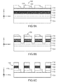
- the figure 4 schematically represents an embodiment of the device 100 according to the second embodiment, forming a module consisting of six LEDs 102.
- the device 100 comprises three LEDs 102a, 102b and 102c electrically connected in series with each other, and three other LEDs 102d, 102e and 102f electrically connected in series with each other and arranged head to tail with the three LEDs 102a, 102b and 102c.
- the cathode of LED 102a which is electrically connected to the anode of LED 102b is also electrically connected to the anode of LED 102d and the cathode of LED 102e.
- the cathode of LED 102b which is electrically connected to the anode of LED 102c is also electrically connected to the anode of LED 102e and the cathode of LED 102f.
- the cathode of LED 102c is electrically connected to the anode of LED 102f
- the anode of the LED 102a is electrically connected to the cathode of the LED 102d.
- the device 100 is electrically powered by applying a supply voltage between two terminals, one being electrically connected to the cathode of the LED 102c (and therefore also to the anode of the LED 102f) and the other being electrically connected. at the anode of LED 102a (and thus also at the cathode of LED 102d).
- the operating voltage of the device 100 is approximately 9V (the operating voltage of each of the LEDs being approximately 3V).
- the LEDs 102a, 102b and 102c being arranged upside down with respect to the LEDs 102d, 102e and 102f, the device 100 is adapted to be electrically powered by an alternating voltage.
- the Figure 5A represents a sectional view of the device 100 along the axis CC shown in FIG. figure 4 , i.e. along the three LEDs 102a, 102b and 102c connected in series with each other.
- the Figure 5B represents a sectional view of the device 100 along the axis BB shown in FIG. figure 4 , i.e., along the three LEDs 102d, 102e and 102f connected in series with each other.
- the visible elements on these Figures 5A and 5B correspond to those previously described in connection with the figure 3 .
- the Figure 5C represents a sectional view of the device 100 along the axis AA represented on the figure 4 , that is to say transversely cutting the LEDs 102b and 102e. It is seen in particular in this figure that electrically conductive material 154 here connects the anode of the LED 102e to the cathode of the LED 102b which is in contact with the portion 120 of the mesa structure of the LED 102b, at the face upper 126 of the second portion 119 of the second doped semiconductor portion 110 of the LED 102b.
- the electrical connection between the cathode of LED 102a and the anode of LED 102d and the electrical connection between the cathode of LED 102b and the anode of LED 102e allow that in case of failure of one of the LEDs this failure does not lead to the formation of an open circuit and to an overall failure of the device 100.
- the device 100 of the figure 4 could include a greater or lesser number of LEDs connected in series to each other. It is also possible to form a device 100 powered by a DC supply voltage by producing the device 100 from a single set of LEDs connected in series with each other, the supply voltage being in this case applied between a first terminal corresponding to the anode of the first LED and a second terminal corresponding to the cathode of the last LED.
- the device 100 it is also possible for the device 100 to include one or more other LEDs making it possible to ensure redundancy of the six LEDs 102a-102f.
- the device 100 could comprise three other LEDs 102 connected in series with each other, this set of three LEDs being connected in parallel with the three LEDs 102a to 102c and thus making it possible to provide redundancy with respect to the three LEDs 102a - 102c. Similar redundancy can be achieved for the three LEDs 102d to 102f with three other LEDs.
- a method of producing the device 100 is described in connection with the Figures 6A to 6K .
- a stack of the different layers intended to form the elements 112, 110, 106, 108 and 114 of the diodes 102 is first made on the substrate 104.
- a hard mask 156 is also formed at the top of this stack of layers.
- the pattern of this hard mask 156 corresponds to that of the mesa structures of the diodes 102 intended to be produced by etching in the stack of layers ( Figure 6A ).
- this mask 156 comprises, opposite the first portion 117 of the second portion of doped semiconductor 110 to be formed, a first portion 157 of greater thickness than a second portion 159 of the mask disposed facing the upper face 126 of the second portion 119 of the second doped semiconductor portion 110 intended to be in contact with the second electrode 128 which will be formed.
- the thicknesses of these two parts 157, 159 of the mask 156 are chosen as a function of the speed with which the different materials of the stack of layers will be etched.
- an etching of the stack of layers is performed to a depth level in the semiconductor layer doped n serving to form the portions 110.
- This etching "consumes" the mask 156 to a thickness equal to that of the second portion 159.
- This etching makes it possible to define in the stack of layers a portion of the spaces in which the second electrodes 128 will be realized.
- This etching is then continued through the parts of the stack not covered by the remaining portions of the hard mask 156, which makes it possible to complete the formation of the upper portions 116 of the mesa structures and also to form the lower portions 118 of the mesa structures. ( Figure 6C ).
- the dielectric portions 122 are for example made by a PECVD type deposit (plasma-assisted chemical vapor deposition) or ALD (atomic layer deposition) according to the deposited material. This deposit of dielectric material is made on the lateral flanks of the mesa structures, but also on and between the mesa structures. Only the portions of this deposit covering the lateral flanks are preserved by performing, after deposition, an etching, for example of the RIE (reactive ion etching) type, of the portions of the dielectric material deposited on and between the mesa structures.
- PECVD type deposit plasma-assisted chemical vapor deposition
- ALD atomic layer deposition
- a full-plate deposit of an electrically conductive material 158 is then implemented such that the spaces between the mesa structures of the diodes 102 are filled with this electrically conductive material.
- the deposited electrically conductive material also covers the mesa structures in view of the full plate deposit produced.
- a chemical mechanical planarization is then implemented with stopping at the upper faces of the dielectric portions 122 in order to remove the portions of the electrically conductive material 158 covering the mesa structures.
- the remaining electrically conductive material forms the second electrodes 128, i.e. the cathodes of the diodes 102 ( figure 6F ). Since the abrasion rate of the metal forming the electrodes 114 and 128 is greater than that of the dielectric material of the portions 122, this CMP step can form slight depressions at the electrodes 114 and 128 with respect to the upper faces of the portions. dielectric 122, as previously described.
- the upper face obtained, however, remains substantially flat and well adapted for subsequent hybridization, for example by direct bonding.
- a dielectric layer 161 is then deposited on the assembly previously made. Lithography and etching are then implemented in order to define the dielectric elements 134 of the future connection structure 132, and cavities, between these dielectric elements 134, defining the locations of the future electrically conductive elements of the connection structure 132 ( Figure 6H ).
- the pattern of this lithography is chosen in particular according to the desired electrical connections for the diodes 102 (serialization, individual connections of each electrode, etc.).
- Another full plate deposit of at least one electrically conductive material 160 is made ( figure 6l ).
- This deposition of electrically conductive material may for example correspond to the implementation of a titanium deposition first to a thickness of about 10 nm, then a second deposit of aluminum to a thickness of about 3 microns. This or these electrically conductive materials fill in particular the spaces between the dielectric elements 134.
- a chemical mechanical planarization is carried out with a stop on the dielectric elements 134, thus defining the electrically conductive elements 150 connected to the anodes and the cathodes of the diodes 102, as well as the electrically conducting elements 152 forming the contact pads of the connection structure 132 On the example of the figure 6J , the electrically conductive elements connect in series the diodes 102.
- the electronic device 100 thus obtained corresponds to that previously described in connection with the figure 2 .
- connection structure 132 As shown on the figure 6K it is possible to complete the connection structure 132 by producing a dielectric deposit 162 covering the electrically conductive elements 150, followed by etching of this dielectric at the level of the electrically conductive elements 152 intended to form the access pads of the device 100, then depositing a metal to extend these access pads next to the dielectric deposit 162.
- the electrically conductive elements 150 forming the connections between the diodes 102 of the device 100 have not been accessible since the outside of the device 100. Only the pads of electrical contacts 164 are accessible from outside the device 100.
Applications Claiming Priority (1)
| Application Number | Priority Date | Filing Date | Title |
|---|---|---|---|
| FR1456085A FR3023061B1 (fr) | 2014-06-27 | 2014-06-27 | Diode de structure mesa a surface de contact sensiblement plane |
Publications (2)
| Publication Number | Publication Date |
|---|---|
| EP2960940A1 true EP2960940A1 (de) | 2015-12-30 |
| EP2960940B1 EP2960940B1 (de) | 2017-03-22 |
Family
ID=51298888
Family Applications (1)
| Application Number | Title | Priority Date | Filing Date |
|---|---|---|---|
| EP15173564.4A Active EP2960940B1 (de) | 2014-06-27 | 2015-06-24 | Diode mit mesastruktur und im wesentlichen ebener kontaktfläche |
Country Status (3)
| Country | Link |
|---|---|
| US (1) | US9608037B2 (de) |
| EP (1) | EP2960940B1 (de) |
| FR (1) | FR3023061B1 (de) |
Cited By (8)
| Publication number | Priority date | Publication date | Assignee | Title |
|---|---|---|---|---|
| EP3070752A1 (de) | 2015-03-20 | 2016-09-21 | Commissariat A L'energie Atomique Et Aux Energies Alternatives | Optoelektronische vorrichtung mit leuchtdiode |
| WO2018122520A1 (fr) | 2016-12-27 | 2018-07-05 | Aledia | Procede de fabrication d'un dispositif optoelectronique comportant des plots photoluminescents de photoresine |
| FR3062953A1 (fr) * | 2017-02-15 | 2018-08-17 | Commissariat A L'energie Atomique Et Aux Energies Alternatives | Dispositif comportant une pluralite de diodes |
| WO2019129978A1 (fr) | 2017-12-27 | 2019-07-04 | Aledia | Dispositif optoelectronique a matrice de diodes tridimensionnelles |
| WO2019202258A2 (fr) | 2018-04-20 | 2019-10-24 | Commissariat à l'énergie atomique et aux énergies alternatives | Procede de fabrication d'un dispositif optoelectronique a matrice de diodes |
| WO2020104495A1 (fr) * | 2018-11-22 | 2020-05-28 | Aledia | Diode électroluminescente et procédé de fabrication d'une diode électroluminescente |
| FR3094141A1 (fr) | 2019-03-18 | 2020-09-25 | Commissariat à l'Energie Atomique et aux Energies Alternatives | procede de fabrication d’un composant optoelectronique a transmission optique en face arriere |
| FR3102613A1 (fr) * | 2019-10-28 | 2021-04-30 | Commissariat A L'energie Atomique Et Aux Energies Alternatives | Procede de realisation d’une diode photo-emettrice ou photo-receptrice |
Families Citing this family (8)
| Publication number | Priority date | Publication date | Assignee | Title |
|---|---|---|---|---|
| US8816383B2 (en) * | 2012-07-06 | 2014-08-26 | Invensas Corporation | High performance light emitting diode with vias |
| FR3023065B1 (fr) * | 2014-06-27 | 2017-12-15 | Commissariat Energie Atomique | Dispositif optoelectronique a jonction p-n permettant une ionisation de dopants par effet de champ |
| FR3057706B1 (fr) | 2016-10-19 | 2018-12-07 | Commissariat A L'energie Atomique Et Aux Energies Alternatives | Procede de realisation d’une puce microelectronique destinee a etre hybridee a une deuxieme puce |
| WO2018137139A1 (en) * | 2017-01-24 | 2018-08-02 | Goertek. Inc | Micro-led device, display apparatus and method for manufacturing a micro-led device |
| TWI653751B (zh) * | 2017-12-05 | 2019-03-11 | 宏碁股份有限公司 | 具修補架構之微型化發光裝置及相關製造和修補方法 |
| WO2019147589A1 (en) * | 2018-01-24 | 2019-08-01 | Apple Inc. | Micro led based display panel |
| WO2019170226A1 (de) * | 2018-03-07 | 2019-09-12 | Photonik Inkubator Gmbh | Halbleiter-vorrichtung zum aussenden von elektromagnetischer strahlung und herstellungsverfahren für dieselbe |
| KR20220014388A (ko) * | 2020-07-24 | 2022-02-07 | 삼성디스플레이 주식회사 | 발광 소자, 이의 제조 방법 및 표시 장치 |
Citations (7)
| Publication number | Priority date | Publication date | Assignee | Title |
|---|---|---|---|---|
| US5952681A (en) * | 1997-11-24 | 1999-09-14 | Chen; Hsing | Light emitting diode emitting red, green and blue light |
| US6957899B2 (en) | 2002-10-24 | 2005-10-25 | Hongxing Jiang | Light emitting diodes for high AC voltage operation and general lighting |
| US7221044B2 (en) | 2005-01-21 | 2007-05-22 | Ac Led Lighting, L.L.C. | Heterogeneous integrated high voltage DC/AC light emitter |
| US8272757B1 (en) | 2005-06-03 | 2012-09-25 | Ac Led Lighting, L.L.C. | Light emitting diode lamp capable of high AC/DC voltage operation |
| US20130105825A1 (en) | 2011-10-26 | 2013-05-02 | Phostek, Inc. | Light emitting diode array |
| FR2992465A1 (fr) * | 2012-06-22 | 2013-12-27 | Soitec Silicon On Insulator | Procede de fabrication collective de leds et structure pour la fabrication collective de leds |
| US20140159063A1 (en) * | 2012-12-07 | 2014-06-12 | Micron Technology, Inc. | Vertical solid-state transducers and high voltage solid-state transducers having buried contacts and associated systems and methods |
Family Cites Families (13)
| Publication number | Priority date | Publication date | Assignee | Title |
|---|---|---|---|---|
| US6547249B2 (en) * | 2001-03-29 | 2003-04-15 | Lumileds Lighting U.S., Llc | Monolithic series/parallel led arrays formed on highly resistive substrates |
| US7067849B2 (en) * | 2001-07-17 | 2006-06-27 | Lg Electronics Inc. | Diode having high brightness and method thereof |
| US7213942B2 (en) * | 2002-10-24 | 2007-05-08 | Ac Led Lighting, L.L.C. | Light emitting diodes for high AC voltage operation and general lighting |
| JP4330476B2 (ja) * | 2004-03-29 | 2009-09-16 | スタンレー電気株式会社 | 半導体発光素子 |
| KR100974923B1 (ko) * | 2007-03-19 | 2010-08-10 | 서울옵토디바이스주식회사 | 발광 다이오드 |
| KR20100095666A (ko) | 2009-02-12 | 2010-09-01 | 서울반도체 주식회사 | 고전압 구동용 발광 다이오드 칩 및 그것을 갖는 발광 다이오드 패키지 |
| TWM374153U (en) * | 2009-03-19 | 2010-02-11 | Intematix Technology Ct Corp | Light emitting device applied to AC drive |
| JP5356312B2 (ja) * | 2010-05-24 | 2013-12-04 | 株式会社東芝 | 半導体発光装置 |
| US9269878B2 (en) * | 2011-05-27 | 2016-02-23 | Lg Innotek Co., Ltd. | Light emitting device and light emitting apparatus |
| FR2976123B1 (fr) | 2011-06-01 | 2013-07-05 | Commissariat Energie Atomique | Structure semiconductrice destinee a emettre de la lumiere et procede de fabrication d'une telle structure |
| FR2997551B1 (fr) | 2012-10-26 | 2015-12-25 | Commissariat Energie Atomique | Procede de fabrication d'une structure semiconductrice et composant semiconducteur comportant une telle structure |
| KR20140073351A (ko) * | 2012-12-06 | 2014-06-16 | 엘지이노텍 주식회사 | 발광 소자 |
| FR3010233B1 (fr) | 2013-08-28 | 2017-02-10 | Commissariat Energie Atomique | Structure semiconductrice a zones d'emission commutables, procede de fabrication d'une telle structure et dispositif semiconducteur comportant une telle structure |
-
2014
- 2014-06-27 FR FR1456085A patent/FR3023061B1/fr active Active
-
2015
- 2015-06-24 EP EP15173564.4A patent/EP2960940B1/de active Active
- 2015-06-24 US US14/748,707 patent/US9608037B2/en active Active
Patent Citations (7)
| Publication number | Priority date | Publication date | Assignee | Title |
|---|---|---|---|---|
| US5952681A (en) * | 1997-11-24 | 1999-09-14 | Chen; Hsing | Light emitting diode emitting red, green and blue light |
| US6957899B2 (en) | 2002-10-24 | 2005-10-25 | Hongxing Jiang | Light emitting diodes for high AC voltage operation and general lighting |
| US7221044B2 (en) | 2005-01-21 | 2007-05-22 | Ac Led Lighting, L.L.C. | Heterogeneous integrated high voltage DC/AC light emitter |
| US8272757B1 (en) | 2005-06-03 | 2012-09-25 | Ac Led Lighting, L.L.C. | Light emitting diode lamp capable of high AC/DC voltage operation |
| US20130105825A1 (en) | 2011-10-26 | 2013-05-02 | Phostek, Inc. | Light emitting diode array |
| FR2992465A1 (fr) * | 2012-06-22 | 2013-12-27 | Soitec Silicon On Insulator | Procede de fabrication collective de leds et structure pour la fabrication collective de leds |
| US20140159063A1 (en) * | 2012-12-07 | 2014-06-12 | Micron Technology, Inc. | Vertical solid-state transducers and high voltage solid-state transducers having buried contacts and associated systems and methods |
Cited By (14)
| Publication number | Priority date | Publication date | Assignee | Title |
|---|---|---|---|---|
| EP3070752A1 (de) | 2015-03-20 | 2016-09-21 | Commissariat A L'energie Atomique Et Aux Energies Alternatives | Optoelektronische vorrichtung mit leuchtdiode |
| WO2018122520A1 (fr) | 2016-12-27 | 2018-07-05 | Aledia | Procede de fabrication d'un dispositif optoelectronique comportant des plots photoluminescents de photoresine |
| US10475849B2 (en) | 2017-02-15 | 2019-11-12 | Commissariat à l'énergie atomique et aux énergies alternatives | Device comprising a plurality of diodes |
| FR3062953A1 (fr) * | 2017-02-15 | 2018-08-17 | Commissariat A L'energie Atomique Et Aux Energies Alternatives | Dispositif comportant une pluralite de diodes |
| EP3364466A1 (de) * | 2017-02-15 | 2018-08-22 | Commissariat à l'Energie Atomique et aux Energies Alternatives | Vorrichtung, die eine vielzahl von dioden umfasst |
| US10361247B2 (en) | 2017-02-15 | 2019-07-23 | Commissariat à l'énergie atomique et aux énergies alternatives | Device comprising a plurality of diodes |
| WO2019129978A1 (fr) | 2017-12-27 | 2019-07-04 | Aledia | Dispositif optoelectronique a matrice de diodes tridimensionnelles |
| WO2019202258A2 (fr) | 2018-04-20 | 2019-10-24 | Commissariat à l'énergie atomique et aux énergies alternatives | Procede de fabrication d'un dispositif optoelectronique a matrice de diodes |
| US11374147B2 (en) | 2018-04-20 | 2022-06-28 | Commissariat à l'énergie atomique et aux énergies alternatives | Process for manufacturing an optoelectronic device having a diode matrix |
| WO2020104495A1 (fr) * | 2018-11-22 | 2020-05-28 | Aledia | Diode électroluminescente et procédé de fabrication d'une diode électroluminescente |
| CN113169207A (zh) * | 2018-11-22 | 2021-07-23 | 艾利迪公司 | 发光二极管及用于制造发光二极管的方法 |
| FR3094141A1 (fr) | 2019-03-18 | 2020-09-25 | Commissariat à l'Energie Atomique et aux Energies Alternatives | procede de fabrication d’un composant optoelectronique a transmission optique en face arriere |
| FR3102613A1 (fr) * | 2019-10-28 | 2021-04-30 | Commissariat A L'energie Atomique Et Aux Energies Alternatives | Procede de realisation d’une diode photo-emettrice ou photo-receptrice |
| EP3817054A1 (de) * | 2019-10-28 | 2021-05-05 | Commissariat à l'énergie atomique et aux énergies alternatives | Verfahren zur herstellung einer lichtemittierenden oder lichtempfangenden diode |
Also Published As
| Publication number | Publication date |
|---|---|
| FR3023061A1 (fr) | 2016-01-01 |
| EP2960940B1 (de) | 2017-03-22 |
| US9608037B2 (en) | 2017-03-28 |
| FR3023061B1 (fr) | 2017-12-15 |
| US20150380459A1 (en) | 2015-12-31 |
Similar Documents
| Publication | Publication Date | Title |
|---|---|---|
| EP2960940B1 (de) | Diode mit mesastruktur und im wesentlichen ebener kontaktfläche | |
| FR3042913B1 (fr) | Diode micro-electronique a surface active optimisee | |
| EP2960951B1 (de) | Optoelektronische vorrichtung mit p-n-übergang, die eine ionisierung der dotierungsmittel durch feldeffekt ermöglicht | |
| EP3171404B1 (de) | Optoelektronische vorrichtung mit leuchtdioden, die mindestens eine zener-diode umfasst | |
| EP3161865B1 (de) | Optoelektronische vorrichtung mit leuchtdioden auf einer steuerschaltung | |
| EP2710634B1 (de) | Elektrische reihenschaltung von lichtemittierenden nanodrähten | |
| EP3817054B1 (de) | Verfahren zur herstellung mindestens einer lichtemittierenden oder lichtempfangenden diode | |
| FR2992465A1 (fr) | Procede de fabrication collective de leds et structure pour la fabrication collective de leds | |
| CN103311261A (zh) | 集成led发光器件及其制作方法 | |
| EP3347917B1 (de) | Elektrolumineszente vorrichtung mit integriertem lichtsensor | |
| FR2964498A1 (fr) | Empilement de led de couleur | |
| EP3740974B1 (de) | Optoelektronische vorrichtung umfassend ein gitter und eine kathode gekoppelt miteinander | |
| EP3732725B1 (de) | Optoelektronische vorrichtung mit einer matrix aus dreidimensionalen dioden | |
| EP3750189B1 (de) | Optoelektronische vorrichtung mit elektronischen bauelementen auf der rückseite des substrats und herstellungsverfahren | |
| FR3009653A1 (fr) | Dispositif de conversion d'energie thermique en energie electrique | |
| EP3351057B1 (de) | Leistungsverwaltung für eine mikro- oder nanodraht-led-lichtquelle | |
| WO2020240140A1 (fr) | Dispositif optoélectronique comportant deux diodes électroluminescentes filaires ayant chacune une couche limitant les courants de fuite |
Legal Events
| Date | Code | Title | Description |
|---|---|---|---|
| PUAI | Public reference made under article 153(3) epc to a published international application that has entered the european phase |
Free format text: ORIGINAL CODE: 0009012 |
|
| AK | Designated contracting states |
Kind code of ref document: A1 Designated state(s): AL AT BE BG CH CY CZ DE DK EE ES FI FR GB GR HR HU IE IS IT LI LT LU LV MC MK MT NL NO PL PT RO RS SE SI SK SM TR |
|
| AX | Request for extension of the european patent |
Extension state: BA ME |
|
| 17P | Request for examination filed |
Effective date: 20160608 |
|
| RBV | Designated contracting states (corrected) |
Designated state(s): AL AT BE BG CH CY CZ DE DK EE ES FI FR GB GR HR HU IE IS IT LI LT LU LV MC MK MT NL NO PL PT RO RS SE SI SK SM TR |
|
| GRAP | Despatch of communication of intention to grant a patent |
Free format text: ORIGINAL CODE: EPIDOSNIGR1 |
|
| RIC1 | Information provided on ipc code assigned before grant |
Ipc: H01L 33/62 20100101ALN20161003BHEP Ipc: H01L 33/20 20100101ALN20161003BHEP Ipc: H01L 27/15 20060101AFI20161003BHEP Ipc: H01L 33/38 20100101ALI20161003BHEP Ipc: H01L 27/144 20060101ALI20161003BHEP Ipc: H01L 31/0224 20060101ALI20161003BHEP Ipc: H01L 27/146 20060101ALI20161003BHEP Ipc: H01L 31/18 20060101ALI20161003BHEP Ipc: H01L 31/0352 20060101ALI20161003BHEP Ipc: H01L 31/02 20060101ALI20161003BHEP |
|
| INTG | Intention to grant announced |
Effective date: 20161020 |
|
| STAA | Information on the status of an ep patent application or granted ep patent |
Free format text: STATUS: GRANT OF PATENT IS INTENDED |
|
| GRAS | Grant fee paid |
Free format text: ORIGINAL CODE: EPIDOSNIGR3 |
|
| GRAA | (expected) grant |
Free format text: ORIGINAL CODE: 0009210 |
|
| STAA | Information on the status of an ep patent application or granted ep patent |
Free format text: STATUS: THE PATENT HAS BEEN GRANTED |
|
| AK | Designated contracting states |
Kind code of ref document: B1 Designated state(s): AL AT BE BG CH CY CZ DE DK EE ES FI FR GB GR HR HU IE IS IT LI LT LU LV MC MK MT NL NO PL PT RO RS SE SI SK SM TR |
|
| REG | Reference to a national code |
Ref country code: GB Ref legal event code: FG4D Free format text: NOT ENGLISH |
|
| REG | Reference to a national code |
Ref country code: CH Ref legal event code: EP |
|
| REG | Reference to a national code |
Ref country code: AT Ref legal event code: REF Ref document number: 878538 Country of ref document: AT Kind code of ref document: T Effective date: 20170415 |
|
| REG | Reference to a national code |
Ref country code: IE Ref legal event code: FG4D Free format text: LANGUAGE OF EP DOCUMENT: FRENCH |
|
| REG | Reference to a national code |
Ref country code: DE Ref legal event code: R096 Ref document number: 602015001905 Country of ref document: DE |
|
| REG | Reference to a national code |
Ref country code: FR Ref legal event code: PLFP Year of fee payment: 3 |
|
| REG | Reference to a national code |
Ref country code: NL Ref legal event code: MP Effective date: 20170322 |
|
| PG25 | Lapsed in a contracting state [announced via postgrant information from national office to epo] |
Ref country code: HR Free format text: LAPSE BECAUSE OF FAILURE TO SUBMIT A TRANSLATION OF THE DESCRIPTION OR TO PAY THE FEE WITHIN THE PRESCRIBED TIME-LIMIT Effective date: 20170322 Ref country code: LT Free format text: LAPSE BECAUSE OF FAILURE TO SUBMIT A TRANSLATION OF THE DESCRIPTION OR TO PAY THE FEE WITHIN THE PRESCRIBED TIME-LIMIT Effective date: 20170322 Ref country code: GR Free format text: LAPSE BECAUSE OF FAILURE TO SUBMIT A TRANSLATION OF THE DESCRIPTION OR TO PAY THE FEE WITHIN THE PRESCRIBED TIME-LIMIT Effective date: 20170623 Ref country code: NO Free format text: LAPSE BECAUSE OF FAILURE TO SUBMIT A TRANSLATION OF THE DESCRIPTION OR TO PAY THE FEE WITHIN THE PRESCRIBED TIME-LIMIT Effective date: 20170622 Ref country code: FI Free format text: LAPSE BECAUSE OF FAILURE TO SUBMIT A TRANSLATION OF THE DESCRIPTION OR TO PAY THE FEE WITHIN THE PRESCRIBED TIME-LIMIT Effective date: 20170322 |
|
| REG | Reference to a national code |
Ref country code: LT Ref legal event code: MG4D |
|
| REG | Reference to a national code |
Ref country code: AT Ref legal event code: MK05 Ref document number: 878538 Country of ref document: AT Kind code of ref document: T Effective date: 20170322 |
|
| PG25 | Lapsed in a contracting state [announced via postgrant information from national office to epo] |
Ref country code: LV Free format text: LAPSE BECAUSE OF FAILURE TO SUBMIT A TRANSLATION OF THE DESCRIPTION OR TO PAY THE FEE WITHIN THE PRESCRIBED TIME-LIMIT Effective date: 20170322 Ref country code: BG Free format text: LAPSE BECAUSE OF FAILURE TO SUBMIT A TRANSLATION OF THE DESCRIPTION OR TO PAY THE FEE WITHIN THE PRESCRIBED TIME-LIMIT Effective date: 20170622 Ref country code: RS Free format text: LAPSE BECAUSE OF FAILURE TO SUBMIT A TRANSLATION OF THE DESCRIPTION OR TO PAY THE FEE WITHIN THE PRESCRIBED TIME-LIMIT Effective date: 20170322 Ref country code: SE Free format text: LAPSE BECAUSE OF FAILURE TO SUBMIT A TRANSLATION OF THE DESCRIPTION OR TO PAY THE FEE WITHIN THE PRESCRIBED TIME-LIMIT Effective date: 20170322 |
|
| PG25 | Lapsed in a contracting state [announced via postgrant information from national office to epo] |
Ref country code: NL Free format text: LAPSE BECAUSE OF FAILURE TO SUBMIT A TRANSLATION OF THE DESCRIPTION OR TO PAY THE FEE WITHIN THE PRESCRIBED TIME-LIMIT Effective date: 20170322 |
|
| PG25 | Lapsed in a contracting state [announced via postgrant information from national office to epo] |
Ref country code: CZ Free format text: LAPSE BECAUSE OF FAILURE TO SUBMIT A TRANSLATION OF THE DESCRIPTION OR TO PAY THE FEE WITHIN THE PRESCRIBED TIME-LIMIT Effective date: 20170322 Ref country code: AT Free format text: LAPSE BECAUSE OF FAILURE TO SUBMIT A TRANSLATION OF THE DESCRIPTION OR TO PAY THE FEE WITHIN THE PRESCRIBED TIME-LIMIT Effective date: 20170322 Ref country code: EE Free format text: LAPSE BECAUSE OF FAILURE TO SUBMIT A TRANSLATION OF THE DESCRIPTION OR TO PAY THE FEE WITHIN THE PRESCRIBED TIME-LIMIT Effective date: 20170322 Ref country code: IT Free format text: LAPSE BECAUSE OF FAILURE TO SUBMIT A TRANSLATION OF THE DESCRIPTION OR TO PAY THE FEE WITHIN THE PRESCRIBED TIME-LIMIT Effective date: 20170322 Ref country code: SK Free format text: LAPSE BECAUSE OF FAILURE TO SUBMIT A TRANSLATION OF THE DESCRIPTION OR TO PAY THE FEE WITHIN THE PRESCRIBED TIME-LIMIT Effective date: 20170322 Ref country code: RO Free format text: LAPSE BECAUSE OF FAILURE TO SUBMIT A TRANSLATION OF THE DESCRIPTION OR TO PAY THE FEE WITHIN THE PRESCRIBED TIME-LIMIT Effective date: 20170322 Ref country code: ES Free format text: LAPSE BECAUSE OF FAILURE TO SUBMIT A TRANSLATION OF THE DESCRIPTION OR TO PAY THE FEE WITHIN THE PRESCRIBED TIME-LIMIT Effective date: 20170322 |
|
| PG25 | Lapsed in a contracting state [announced via postgrant information from national office to epo] |
Ref country code: SM Free format text: LAPSE BECAUSE OF FAILURE TO SUBMIT A TRANSLATION OF THE DESCRIPTION OR TO PAY THE FEE WITHIN THE PRESCRIBED TIME-LIMIT Effective date: 20170322 Ref country code: PL Free format text: LAPSE BECAUSE OF FAILURE TO SUBMIT A TRANSLATION OF THE DESCRIPTION OR TO PAY THE FEE WITHIN THE PRESCRIBED TIME-LIMIT Effective date: 20170322 Ref country code: IS Free format text: LAPSE BECAUSE OF FAILURE TO SUBMIT A TRANSLATION OF THE DESCRIPTION OR TO PAY THE FEE WITHIN THE PRESCRIBED TIME-LIMIT Effective date: 20170722 Ref country code: PT Free format text: LAPSE BECAUSE OF FAILURE TO SUBMIT A TRANSLATION OF THE DESCRIPTION OR TO PAY THE FEE WITHIN THE PRESCRIBED TIME-LIMIT Effective date: 20170724 |
|
| REG | Reference to a national code |
Ref country code: DE Ref legal event code: R097 Ref document number: 602015001905 Country of ref document: DE |
|
| PLBE | No opposition filed within time limit |
Free format text: ORIGINAL CODE: 0009261 |
|
| STAA | Information on the status of an ep patent application or granted ep patent |
Free format text: STATUS: NO OPPOSITION FILED WITHIN TIME LIMIT |
|
| PG25 | Lapsed in a contracting state [announced via postgrant information from national office to epo] |
Ref country code: DK Free format text: LAPSE BECAUSE OF FAILURE TO SUBMIT A TRANSLATION OF THE DESCRIPTION OR TO PAY THE FEE WITHIN THE PRESCRIBED TIME-LIMIT Effective date: 20170322 Ref country code: MC Free format text: LAPSE BECAUSE OF FAILURE TO SUBMIT A TRANSLATION OF THE DESCRIPTION OR TO PAY THE FEE WITHIN THE PRESCRIBED TIME-LIMIT Effective date: 20170322 |
|
| 26N | No opposition filed |
Effective date: 20180102 |
|
| PG25 | Lapsed in a contracting state [announced via postgrant information from national office to epo] |
Ref country code: SI Free format text: LAPSE BECAUSE OF FAILURE TO SUBMIT A TRANSLATION OF THE DESCRIPTION OR TO PAY THE FEE WITHIN THE PRESCRIBED TIME-LIMIT Effective date: 20170322 |
|
| REG | Reference to a national code |
Ref country code: IE Ref legal event code: MM4A |
|
| PG25 | Lapsed in a contracting state [announced via postgrant information from national office to epo] |
Ref country code: LU Free format text: LAPSE BECAUSE OF NON-PAYMENT OF DUE FEES Effective date: 20170624 Ref country code: IE Free format text: LAPSE BECAUSE OF NON-PAYMENT OF DUE FEES Effective date: 20170624 |
|
| REG | Reference to a national code |
Ref country code: BE Ref legal event code: MM Effective date: 20170630 |
|
| REG | Reference to a national code |
Ref country code: FR Ref legal event code: PLFP Year of fee payment: 4 |
|
| PG25 | Lapsed in a contracting state [announced via postgrant information from national office to epo] |
Ref country code: BE Free format text: LAPSE BECAUSE OF NON-PAYMENT OF DUE FEES Effective date: 20170630 |
|
| PG25 | Lapsed in a contracting state [announced via postgrant information from national office to epo] |
Ref country code: MT Free format text: LAPSE BECAUSE OF FAILURE TO SUBMIT A TRANSLATION OF THE DESCRIPTION OR TO PAY THE FEE WITHIN THE PRESCRIBED TIME-LIMIT Effective date: 20170322 |
|
| REG | Reference to a national code |
Ref country code: CH Ref legal event code: PL |
|
| PG25 | Lapsed in a contracting state [announced via postgrant information from national office to epo] |
Ref country code: LI Free format text: LAPSE BECAUSE OF NON-PAYMENT OF DUE FEES Effective date: 20180630 Ref country code: CH Free format text: LAPSE BECAUSE OF NON-PAYMENT OF DUE FEES Effective date: 20180630 |
|
| PG25 | Lapsed in a contracting state [announced via postgrant information from national office to epo] |
Ref country code: HU Free format text: LAPSE BECAUSE OF FAILURE TO SUBMIT A TRANSLATION OF THE DESCRIPTION OR TO PAY THE FEE WITHIN THE PRESCRIBED TIME-LIMIT; INVALID AB INITIO Effective date: 20150624 |
|
| PG25 | Lapsed in a contracting state [announced via postgrant information from national office to epo] |
Ref country code: CY Free format text: LAPSE BECAUSE OF FAILURE TO SUBMIT A TRANSLATION OF THE DESCRIPTION OR TO PAY THE FEE WITHIN THE PRESCRIBED TIME-LIMIT Effective date: 20170322 |
|
| PG25 | Lapsed in a contracting state [announced via postgrant information from national office to epo] |
Ref country code: MK Free format text: LAPSE BECAUSE OF FAILURE TO SUBMIT A TRANSLATION OF THE DESCRIPTION OR TO PAY THE FEE WITHIN THE PRESCRIBED TIME-LIMIT Effective date: 20170322 |
|
| PG25 | Lapsed in a contracting state [announced via postgrant information from national office to epo] |
Ref country code: TR Free format text: LAPSE BECAUSE OF FAILURE TO SUBMIT A TRANSLATION OF THE DESCRIPTION OR TO PAY THE FEE WITHIN THE PRESCRIBED TIME-LIMIT Effective date: 20170322 |
|
| PG25 | Lapsed in a contracting state [announced via postgrant information from national office to epo] |
Ref country code: AL Free format text: LAPSE BECAUSE OF FAILURE TO SUBMIT A TRANSLATION OF THE DESCRIPTION OR TO PAY THE FEE WITHIN THE PRESCRIBED TIME-LIMIT Effective date: 20170322 |
|
| PGFP | Annual fee paid to national office [announced via postgrant information from national office to epo] |
Ref country code: FR Payment date: 20230623 Year of fee payment: 9 Ref country code: DE Payment date: 20230620 Year of fee payment: 9 |
|
| PGFP | Annual fee paid to national office [announced via postgrant information from national office to epo] |
Ref country code: GB Payment date: 20230622 Year of fee payment: 9 |