EP2960696B1 - Optical system - Google Patents
Optical system Download PDFInfo
- Publication number
- EP2960696B1 EP2960696B1 EP15173146.0A EP15173146A EP2960696B1 EP 2960696 B1 EP2960696 B1 EP 2960696B1 EP 15173146 A EP15173146 A EP 15173146A EP 2960696 B1 EP2960696 B1 EP 2960696B1
- Authority
- EP
- European Patent Office
- Prior art keywords
- lens elements
- optical system
- optical
- light emitting
- light
- Prior art date
- Legal status (The legal status is an assumption and is not a legal conclusion. Google has not performed a legal analysis and makes no representation as to the accuracy of the status listed.)
- Active
Links
Images


Classifications
-
- G—PHYSICS
- G02—OPTICS
- G02B—OPTICAL ELEMENTS, SYSTEMS OR APPARATUS
- G02B27/00—Optical systems or apparatus not provided for by any of the groups G02B1/00 - G02B26/00, G02B30/00
- G02B27/09—Beam shaping, e.g. changing the cross-sectional area, not otherwise provided for
- G02B27/0916—Adapting the beam shape of a semiconductor light source such as a laser diode or an LED, e.g. for efficiently coupling into optical fibers
- G02B27/0922—Adapting the beam shape of a semiconductor light source such as a laser diode or an LED, e.g. for efficiently coupling into optical fibers the semiconductor light source comprising an array of light emitters
-
- G—PHYSICS
- G02—OPTICS
- G02B—OPTICAL ELEMENTS, SYSTEMS OR APPARATUS
- G02B19/00—Condensers, e.g. light collectors or similar non-imaging optics
- G02B19/0004—Condensers, e.g. light collectors or similar non-imaging optics characterised by the optical means employed
- G02B19/0009—Condensers, e.g. light collectors or similar non-imaging optics characterised by the optical means employed having refractive surfaces only
- G02B19/0014—Condensers, e.g. light collectors or similar non-imaging optics characterised by the optical means employed having refractive surfaces only at least one surface having optical power
-
- G—PHYSICS
- G02—OPTICS
- G02B—OPTICAL ELEMENTS, SYSTEMS OR APPARATUS
- G02B27/00—Optical systems or apparatus not provided for by any of the groups G02B1/00 - G02B26/00, G02B30/00
- G02B27/09—Beam shaping, e.g. changing the cross-sectional area, not otherwise provided for
- G02B27/0938—Using specific optical elements
- G02B27/095—Refractive optical elements
- G02B27/0955—Lenses
- G02B27/0961—Lens arrays
-
- G—PHYSICS
- G02—OPTICS
- G02B—OPTICAL ELEMENTS, SYSTEMS OR APPARATUS
- G02B19/00—Condensers, e.g. light collectors or similar non-imaging optics
- G02B19/0033—Condensers, e.g. light collectors or similar non-imaging optics characterised by the use
- G02B19/0047—Condensers, e.g. light collectors or similar non-imaging optics characterised by the use for use with a light source
- G02B19/0052—Condensers, e.g. light collectors or similar non-imaging optics characterised by the use for use with a light source the light source comprising a laser diode
- G02B19/0057—Condensers, e.g. light collectors or similar non-imaging optics characterised by the use for use with a light source the light source comprising a laser diode in the form of a laser diode array, e.g. laser diode bar
-
- G—PHYSICS
- G02—OPTICS
- G02B—OPTICAL ELEMENTS, SYSTEMS OR APPARATUS
- G02B3/00—Simple or compound lenses
- G02B3/0006—Arrays
- G02B3/0037—Arrays characterized by the distribution or form of lenses
- G02B3/005—Arrays characterized by the distribution or form of lenses arranged along a single direction only, e.g. lenticular sheets
-
- G—PHYSICS
- G02—OPTICS
- G02B—OPTICAL ELEMENTS, SYSTEMS OR APPARATUS
- G02B6/00—Light guides; Structural details of arrangements comprising light guides and other optical elements, e.g. couplings
- G02B6/24—Coupling light guides
- G02B6/42—Coupling light guides with opto-electronic elements
- G02B6/4201—Packages, e.g. shape, construction, internal or external details
- G02B6/4204—Packages, e.g. shape, construction, internal or external details the coupling comprising intermediate optical elements, e.g. lenses, holograms
- G02B6/4206—Optical features
-
- H—ELECTRICITY
- H01—ELECTRIC ELEMENTS
- H01S—DEVICES USING THE PROCESS OF LIGHT AMPLIFICATION BY STIMULATED EMISSION OF RADIATION [LASER] TO AMPLIFY OR GENERATE LIGHT; DEVICES USING STIMULATED EMISSION OF ELECTROMAGNETIC RADIATION IN WAVE RANGES OTHER THAN OPTICAL
- H01S3/00—Lasers, i.e. devices using stimulated emission of electromagnetic radiation in the infrared, visible or ultraviolet wave range
- H01S3/09—Processes or apparatus for excitation, e.g. pumping
- H01S3/091—Processes or apparatus for excitation, e.g. pumping using optical pumping
- H01S3/094—Processes or apparatus for excitation, e.g. pumping using optical pumping by coherent light
- H01S3/094003—Processes or apparatus for excitation, e.g. pumping using optical pumping by coherent light the pumped medium being a fibre
-
- H—ELECTRICITY
- H01—ELECTRIC ELEMENTS
- H01S—DEVICES USING THE PROCESS OF LIGHT AMPLIFICATION BY STIMULATED EMISSION OF RADIATION [LASER] TO AMPLIFY OR GENERATE LIGHT; DEVICES USING STIMULATED EMISSION OF ELECTROMAGNETIC RADIATION IN WAVE RANGES OTHER THAN OPTICAL
- H01S3/00—Lasers, i.e. devices using stimulated emission of electromagnetic radiation in the infrared, visible or ultraviolet wave range
- H01S3/09—Processes or apparatus for excitation, e.g. pumping
- H01S3/091—Processes or apparatus for excitation, e.g. pumping using optical pumping
- H01S3/094—Processes or apparatus for excitation, e.g. pumping using optical pumping by coherent light
- H01S3/0941—Processes or apparatus for excitation, e.g. pumping using optical pumping by coherent light of a laser diode
- H01S3/09415—Processes or apparatus for excitation, e.g. pumping using optical pumping by coherent light of a laser diode the pumping beam being parallel to the lasing mode of the pumped medium, e.g. end-pumping
-
- H—ELECTRICITY
- H01—ELECTRIC ELEMENTS
- H01S—DEVICES USING THE PROCESS OF LIGHT AMPLIFICATION BY STIMULATED EMISSION OF RADIATION [LASER] TO AMPLIFY OR GENERATE LIGHT; DEVICES USING STIMULATED EMISSION OF ELECTROMAGNETIC RADIATION IN WAVE RANGES OTHER THAN OPTICAL
- H01S5/00—Semiconductor lasers
- H01S5/40—Arrangement of two or more semiconductor lasers, not provided for in groups H01S5/02 - H01S5/30
- H01S5/4012—Beam combining, e.g. by the use of fibres, gratings, polarisers, prisms
Definitions
- This disclosure relates to an optical system that guides light beams emitted from a plurality of light emitting parts into an optical fiber.
- Fiber lasers are known as a kind of solid-state laser. Such a fiber laser has a variety of advantages such as good process quality due to its fine light emitting point, good usability, and good maintainability due to its capacity to use a semiconductor laser as an excitation light source.
- excitation light of high intensity may be introduced into the fiber.
- One proposed solution to the above involves the collection of light beams emitted from a plurality of light emitting points into the fiber (Refer to Patent Literature 1).
- US2005/0232628 discloses an optical symmetrization device for symmetrizing the radiation emitted by laser diodes.
- US6407870 discloses an optical system for reshaping the cross section of a beam emitted by laser diodes.
- US5787107 teaches a lens system for forming a two-dimensional pattern of light.
- Patent Literature 1 fails to consider the lifetime of the disclosed device, and a longer lifetime of such a device has been required.
- This disclosure is based on the aforementioned viewpoint. It would be helpful to provide an optical system that is capable of lengthening the lifetime of the fiber, which is one of components of the fiber laser device.
- the optical system according to the invention is capable of lengthening the lifetime of the fiber used in the fiber laser.
- FIG. 1 is an appearance view schematically illustrating a fiber laser device including an optical system according to a first embodiment.
- the fiber laser device 10 includes a light source unit 11, an optical fiber 12, and an optical system 13.
- the light source unit 11 emits light which is excited.
- the optical fiber 12 undergoes laser oscillation by the emitted light.
- the optical system 13 guides the light emitted from the light source unit 11 to the optical fiber 12.
- a first direction d1, a second direction d2, and a third direction d3, which are orthogonal to each other, are defined.
- the light source unit 11 includes a plurality of, e.g., three in the present embodiment, light emitting parts ep arranged along any single direction, and each light emitting part ep emits a light beam.
- the light source unit 11 including the plurality of light emitting parts ep may be a laser bar including light emitting parts ep arranged along any single direction.
- the light source unit 11 may also be configured by a plurality of laser chips arranged along any single direction.
- the light source unit 11 is arranged in a manner such that a direction that the light emitting parts ep are arranged is parallel with the first direction d1.
- the optical fiber 12 has, for example, a double clad structure with a rare earth element-doped core, and light, after entering the first clad and the core, is propagated in the optical fiber 12 while being reflected by an interface between the first clad and the second clad. The light is partly absorbed in the core while being propagated between both ends. By the light partially absorbed, the doped rare earth element is excited, thereby causing laser oscillation in the optical fiber 12.
- the optical system 13 is made of a glass material having a refractive index of greater than or equal to 1.7 and includes a first optical element 14 and a second optical element 15.
- the first optical element 14 and the second optical element 15 may be arranged with space therebetween.
- the optical system 13 may also be configured to include the first optical element 14 and the second optical element 15 that are integrated.
- the first optical element 14 includes an incident surface is that is designed to be located closest to the light emitting parts ep in the optical system 13.
- the incident surface is generally or partially includes a toroidal surface portion.
- the arcuate toroidal surface portion of the first optical element 14 has two sections that are orthogonal to each other and that have a small and a large radius of curvature.
- the first optical element 14 is arranged in a manner such that the section having the small radius of curvature is orthogonal to the first direction d1, and the section having the large radius of curvature is orthogonal to the second direction d2.
- the incident surface is of the first optical element 14 is configured to collect light beams emitted from the light emitting parts ep in a surface constituting lens elements 16a, 16b, and 16c disposed in correspondence with the light emitting parts ep, in the first direction d1.
- the lens elements 16a, 16b, and 16c are later described.
- the incident surface is of the first optical element 14 is configured to collect light beams emitted from the light emitting parts ep in the surface constituting the corresponding lens elements 16a, 16b, and 16c, in the second direction d2.
- the second optical element 15 includes an emission surface es that is designed to be located closest to the optical fiber 12 in the optical system 13 (refer to FIG. 1 ).
- the emission surface es includes a plurality of, e.g., three in the present embodiment, lens elements 16a, 16b, and 16c arranged along any single direction. The number of the lens elements is greater than or equal to that of the light emitting parts ep.
- the lens elements 16a, 16b, and 16c emit the light beams which have entered the first optical element 14 toward the optical fiber 12.
- the plurality of lens element 16a, 16b, and 16c are arranged to be aligned along the first direction d1 in the second optical element 15.
- the lens elements 16a, 16b, and 16c are each formed in a toroidal shape, and the emission surface es has a toroidal surface portion.
- the arcuate toroidal surface of each of the lens elements 16a, 16b, and 16c has two sections that are orthogonal to each other, and the lens elements 16a, 16b, and 16c are arranged in a manner such that these sections are orthogonal to the first direction d1 and the second direction d2.
- the lens elements 16a, 16b, and 16c are configured to collect light beams emitted from the corresponding light emitting parts ep in the first direction d1 and to emit the collected light beams to the single optical fiber 12 located at a predetermined distance from the emission surface es.
- the lens elements e.g., the lens elements 16a and 16c
- the lens elements 16a and 16c except for any one of the lens elements 16a, 16b, and 16c (e.g., the lens element 16b that is located in the middle in the first direction d1), are configured to have optical axes that are eccentric to that of the any one of the lens elements (e.g., the lens element 16b) in the first direction d1.
- the lens elements e.g., the lens elements 16a and 16c
- any one of the lens elements 16a, 16b, and 16c e.g., the lens element 16b
- the lens elements 16a and 16c are configured to have optical axes that are inclined from that of the any one of the lens elements (e.g, the lens element 16b) with respect to a straight line extending in parallel to the second direction.
- the light beams may be collected by the optical system 13 in the first direction d1, not always in a single point, but within a certain width range, and moreover, this width may be greater than the diameter of the first clad included in the optical fiber 12.
- the light collection range does not necessarily be identical for each light beam.
- the lens elements 16a, 16b, and 16c are each configured to collect the light beam emitted from the corresponding light emitting part ep and to emit the collected light beam to the single optical fiber 12 located at the predetermined distance, with the respective light beams emitted from the light emitting parts ep having different light collection centers cc which are offset from each other in the second direction d2 (refer to FIG. 6 ).
- the lens elements 16a, 16b, and 16c are each configured to refract the light beam from the corresponding light emitting part ep into a different orientation in the second direction d2 (refer to FIG. 5 ).
- the lens elements e.g., the lens elements 16a and 16c
- the lens elements 16a and 16c except for any one of the lens elements 16a, 16b, and 16c (e.g., the lens element 16b that is located in the middle in the first direction d1), are configured to have optical axes that are eccentric to that of the any one of the lens elements (e.g., the lens element 16b) in the second direction d2.
- the lens elements e.g., the lens elements 16a and 16c
- any one of the lens elements 16a, 16b, and 16c e.g., the lens element 16b
- the lens elements 16a and 16c are configured to have optical axes that are inclined from that of the any one of the lens elements (e.g, the lens element 16b) with respect to a straight line extending in parallel to the first direction d1.
- the emission surface es is formed to maintain continuity of two adjacent lens elements (16a and 16b) and (16b and 16c) in the third direction d3, which is orthogonal to each of the first direction d1 and the second direction d2.
- the optical system according to the first embodiment with the above structures emits the light beams from the plurality of light emitting parts ep to the single optical fiber 12 while allowing the light collection centers cc of the light beams to be offset from each other in the second direction d2. As a result, the light beams are prevented from entering the optical fiber at a single point. This prevents deterioration of the incident surface is of the optical fiber 12 due to light beams focused on a single point, and accordingly, the lifetime of the optical fiber 12 is lengthened.
- two lens elements (16a and 16b) and (16b and 16c) that are adjacent to each other are contiguous in the third direction d3 when viewed from the second direction d2.
- a difference in level between each two adjacent lens elements is relatively small.
- Such small differences in level of two adjacent lens elements (16a and 16b) and (16b and 16c) provide the following advantageous effect in injection molding of the optical system 13.
- injection molding as differences in level of two adjacent lens elements increase, larger molding loads are required in order to fill the stepped portions with glass, and the more likely it is that the metal mold will be deteriorated.
- Such a metal mold also generally uses, as its material, tungsten carbide and ceramic having relatively low tenacities and is susceptible to chipping in the presence of such differences in level. Accordingly, the present embodiment with the relatively small differences in step is capable of preventing the deterioration of the metal mold in injection molding of the optical system 13.
- the optical system according to the first embodiment is configured by the optical system 13 using the glass material having a refractive index of greater than or equal to 1.7.
- the radius of curvature of the incident surface is of the first optical element 14 measured in a section taken along the plane that is orthogonal to each of the first direction d1 and the second direction d2 is increased, the light beams are sufficiently collected.
- the increased radius of curvature also facilitates manufacturing of the optical system 13.
- the optical system 130 in the second embodiment is made of a glass material having a refractive index of greater than or equal to 1.7 and includes a first optical element 140 and a second optical element 150 as illustrated in FIG. 7 .
- the first optical element 140 and the second optical element 150 may be arranged with space therebetween.
- the optical system 130 may also be configured to include the first optical element 140 and the second optical element 150 that are integrated.
- the incident surface is of the first optical element 140 includes a plurality of, e.g., three in the present embodiment, lens elements 170a, 170b, and 170c arranged along the first direction d1.
- the number of the lens elements is greater than or equal to that of the light emitting parts ep.
- the lens elements 170a, 170b, and 170c included in the incident surface is are each formed in an aspheric shape, and the incident surface is has an aspheric surface.
- the lens elements 170a, 170b, and 170c included in the incident surface is are each positioned with its optical axis orthogonal to the first direction d1.
- the lens elements 170a, 170b, and 170c included in the incident surface is are configured to collect light beams emitted from the light emitting parts ep in a surface constituting lens elements 160a, 160b, and 160c included in the emission surface es that are disposed in correspondence with the light emitting parts ep, in the first direction d1 and the second direction d2.
- the second optical element 150 includes the emission surface es that is designed to be located closest to the optical fiber 12 in the optical system 130.
- the emission surface es includes the plurality of, e.g., three in the present embodiment, lens elements 160a, 160b, and 160c arranged along any single direction. The number of the lens elements is greater than or equal to that of the light emitting parts ep.
- the plurality of lens element 160a, 160b, and 160c are arranged to be aligned along the first direction d1 in the second optical element 150.
- the lens elements 160a, 160b, and 160c are each formed in an aspheric shape.
- the aspheric surfaces of the lens elements 160a, 160b, and 160c are configured to collect light beams emitted from the corresponding light emitting parts ep in the first direction d1 and to emit the collected light beams to the single optical fiber 12 located at a predetermined distance from the emission surface es.
- the aspheric surfaces of the lens elements 160a, 160b, and 160c are also configured to emit the light beams from the plurality of light emitting parts ep to the single optical fiber 12 located at the predetermined distance while allowing the light collection centers cc of the light beams to be offset from each other in the second direction d2.
- the optical system according to the second embodiment with the above structures also prevents the light beams from being guided to a single point in the optical fiber 12 in the second direction d2, and accordingly, the lifetime of the optical fiber 12 is lengthened. Furthermore, in the optical system according to the second embodiment also, as viewed from the second direction d2, the incident surface is and the emission surface es may be formed to maintain continuity of two adjacent lens elements (160a and 160b), (160b and 160c), (170a, 170b), and (170b, 170c) in the third direction d3.
- the optical system according to the second embodiment is configured by the optical system 130 using the glass material having a refractive index of greater than or equal to 1.7. As a result, even when the incident surface is of the first optical element 140 is formed in a planar shape, the light beams are sufficiently collected.
- the incident surface includes an aspheric surface
- the incident surface may also include a spherical or a planar surface.
- the emission surface es may collect, in the surface constituting the lens elements 160a, 160b, and 160c of the emission surface es, the light beams emitted from the corresponding light emitting parts ep.
- the same advantageous effect as that of the second embodiment would be achieved.
Landscapes
- Physics & Mathematics (AREA)
- General Physics & Mathematics (AREA)
- Optics & Photonics (AREA)
- Optical Couplings Of Light Guides (AREA)
- Lasers (AREA)
Description
- This disclosure relates to an optical system that guides light beams emitted from a plurality of light emitting parts into an optical fiber.
- Fiber lasers are known as a kind of solid-state laser. Such a fiber laser has a variety of advantages such as good process quality due to its fine light emitting point, good usability, and good maintainability due to its capacity to use a semiconductor laser as an excitation light source. In response to recent demands for a high output-power fiber laser, excitation light of high intensity may be introduced into the fiber. However, there is limitation on the increase in the output power of the excitation light emitted from a single light emitting point of the semiconductor laser used as the excitation light source. One proposed solution to the above involves the collection of light beams emitted from a plurality of light emitting points into the fiber (Refer to Patent Literature 1).
US2005/0232628 discloses an optical symmetrization device for symmetrizing the radiation emitted by laser diodes.US6407870 discloses an optical system for reshaping the cross section of a beam emitted by laser diodes.US5787107 teaches a lens system for forming a two-dimensional pattern of light. - PTL 1:
JP2011076092A - However, Patent Literature 1 fails to consider the lifetime of the disclosed device, and a longer lifetime of such a device has been required.
- This disclosure is based on the aforementioned viewpoint. It would be helpful to provide an optical system that is capable of lengthening the lifetime of the fiber, which is one of components of the fiber laser device.
- The invention in view of the aforementioned problems resides in an optical system as claimed in claim 1. Further aspects of the invention are defined in the dependent claims.
- The optical system according to the invention is capable of lengthening the lifetime of the fiber used in the fiber laser.
- In the accompanying drawings:
-
FIG. 1 is an appearance view schematically illustrating a structure of a fiber laser device including an optical system according to a first embodiment; -
FIG. 2 is a plan view of a light source unit and the optical system illustrated inFIG. 1 ; -
FIG. 3 is a sectional view taken along a line III-III inFIG. 2 ; -
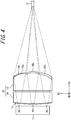
FIG. 4 is a plan view of the fiber laser device ofFIG. 1 , illustrating, along a first direction, a state where light beams are collected according to the optical system illustrated inFIG. 1 ; -
FIG. 5 is a side view of the fiber laser device ofFIG. 1 , illustrating, along a second direction, a state where light beams are collected according to the optical system illustrated inFIG. 1 ; -
FIG. 6 is a front view of an incidence surface of the optical fiber ofFIG. 1 , illustrating, along a second direction, a state where light beams are collected according to the optical system ofFIG. 1 ; and -
FIG. 7 is a plan view of a light source unit and an optical system according to a second embodiment. - Embodiments will be described below with reference to the drawings.
-
FIG. 1 is an appearance view schematically illustrating a fiber laser device including an optical system according to a first embodiment. - The
fiber laser device 10 includes alight source unit 11, anoptical fiber 12, and anoptical system 13. Thelight source unit 11 emits light which is excited. Theoptical fiber 12 undergoes laser oscillation by the emitted light. Theoptical system 13 guides the light emitted from thelight source unit 11 to theoptical fiber 12. In thefiber laser device 10, a first direction d1, a second direction d2, and a third direction d3, which are orthogonal to each other, are defined. - The
light source unit 11 includes a plurality of, e.g., three in the present embodiment, light emitting parts ep arranged along any single direction, and each light emitting part ep emits a light beam. Thelight source unit 11 including the plurality of light emitting parts ep may be a laser bar including light emitting parts ep arranged along any single direction. Thelight source unit 11 may also be configured by a plurality of laser chips arranged along any single direction. Thelight source unit 11 is arranged in a manner such that a direction that the light emitting parts ep are arranged is parallel with the first direction d1. - The
optical fiber 12 has, for example, a double clad structure with a rare earth element-doped core, and light, after entering the first clad and the core, is propagated in theoptical fiber 12 while being reflected by an interface between the first clad and the second clad. The light is partly absorbed in the core while being propagated between both ends. By the light partially absorbed, the doped rare earth element is excited, thereby causing laser oscillation in theoptical fiber 12. - The
optical system 13 is made of a glass material having a refractive index of greater than or equal to 1.7 and includes a firstoptical element 14 and a secondoptical element 15. The firstoptical element 14 and the secondoptical element 15 may be arranged with space therebetween. However, theoptical system 13 may also be configured to include the firstoptical element 14 and the secondoptical element 15 that are integrated. - The first
optical element 14 includes an incident surface is that is designed to be located closest to the light emitting parts ep in theoptical system 13. The incident surface is generally or partially includes a toroidal surface portion. The arcuate toroidal surface portion of the firstoptical element 14 has two sections that are orthogonal to each other and that have a small and a large radius of curvature. The firstoptical element 14 is arranged in a manner such that the section having the small radius of curvature is orthogonal to the first direction d1, and the section having the large radius of curvature is orthogonal to the second direction d2. - As illustrated in
FIG. 2 , the incident surface is of the firstoptical element 14 is configured to collect light beams emitted from the light emitting parts ep in a surface constitutinglens elements lens elements FIG. 3 , the incident surface is of the firstoptical element 14 is configured to collect light beams emitted from the light emitting parts ep in the surface constituting thecorresponding lens elements - The second
optical element 15 includes an emission surface es that is designed to be located closest to theoptical fiber 12 in the optical system 13 (refer toFIG. 1 ). The emission surface es includes a plurality of, e.g., three in the present embodiment,lens elements lens elements optical element 14 toward theoptical fiber 12. The plurality oflens element optical element 15. Thelens elements lens elements lens elements - As illustrated in
FIG. 4 , thelens elements optical fiber 12 located at a predetermined distance from the emission surface es. In order to emit the light beams to theoptical fiber 12, the lens elements (e.g., thelens elements lens elements lens element 16b that is located in the middle in the first direction d1), are configured to have optical axes that are eccentric to that of the any one of the lens elements (e.g., thelens element 16b) in the first direction d1. Alternatively, in order to emit the light beams to theoptical fiber 12, the lens elements (e.g., thelens elements lens elements lens element 16b), are configured to have optical axes that are inclined from that of the any one of the lens elements (e.g, thelens element 16b) with respect to a straight line extending in parallel to the second direction. - Additionally, the light beams may be collected by the
optical system 13 in the first direction d1, not always in a single point, but within a certain width range, and moreover, this width may be greater than the diameter of the first clad included in theoptical fiber 12. Moreover, in the first direction d1, the light collection range does not necessarily be identical for each light beam. - As illustrated in
FIG. 5 , thelens elements optical fiber 12 located at the predetermined distance, with the respective light beams emitted from the light emitting parts ep having different light collection centers cc which are offset from each other in the second direction d2 (refer toFIG. 6 ). In order for the light beams to be emitted to theoptical fiber 12 at the different light collection centers cc which are offset from each other, thelens elements FIG. 5 ). For example, the lens elements (e.g., thelens elements lens elements lens element 16b that is located in the middle in the first direction d1), are configured to have optical axes that are eccentric to that of the any one of the lens elements (e.g., thelens element 16b) in the second direction d2. Alternatively, the lens elements (e.g., thelens elements lens elements lens element 16b), are configured to have optical axes that are inclined from that of the any one of the lens elements (e.g, thelens element 16b) with respect to a straight line extending in parallel to the first direction d1. - Furthermore, as illustrated in
FIG. 2 , as viewed from the second direction d2, the emission surface es is formed to maintain continuity of two adjacent lens elements (16a and 16b) and (16b and 16c) in the third direction d3, which is orthogonal to each of the first direction d1 and the second direction d2. - The optical system according to the first embodiment with the above structures emits the light beams from the plurality of light emitting parts ep to the single
optical fiber 12 while allowing the light collection centers cc of the light beams to be offset from each other in the second direction d2. As a result, the light beams are prevented from entering the optical fiber at a single point. This prevents deterioration of the incident surface is of theoptical fiber 12 due to light beams focused on a single point, and accordingly, the lifetime of theoptical fiber 12 is lengthened. - Moreover, in the optical system according to the first embodiment, two lens elements (16a and 16b) and (16b and 16c) that are adjacent to each other are contiguous in the third direction d3 when viewed from the second direction d2. As a result, a difference in level between each two adjacent lens elements, such as between (16a) and (16b) and between (16b) and (16c), is relatively small. Such small differences in level of two adjacent lens elements (16a and 16b) and (16b and 16c) provide the following advantageous effect in injection molding of the
optical system 13. Generally, in injection molding, as differences in level of two adjacent lens elements increase, larger molding loads are required in order to fill the stepped portions with glass, and the more likely it is that the metal mold will be deteriorated. Such a metal mold also generally uses, as its material, tungsten carbide and ceramic having relatively low tenacities and is susceptible to chipping in the presence of such differences in level. Accordingly, the present embodiment with the relatively small differences in step is capable of preventing the deterioration of the metal mold in injection molding of theoptical system 13. - Moreover, the optical system according to the first embodiment is configured by the
optical system 13 using the glass material having a refractive index of greater than or equal to 1.7. As a result, even when the radius of curvature of the incident surface is of the firstoptical element 14 measured in a section taken along the plane that is orthogonal to each of the first direction d1 and the second direction d2 is increased, the light beams are sufficiently collected. The increased radius of curvature also facilitates manufacturing of theoptical system 13. - In the following, a description is given of the optical system according to a second embodiment. In the optical system according to the second embodiment, structures of the incident surface of the first optical element and the emission surface of the second optical element differ from those according to the first embodiment. The description of the second embodiment below focuses on the differences from the first embodiment. Elements having substantially the same structures as in the first embodiment are designated by the same reference numerals.
- Similarly to the first embodiment, the
optical system 130 in the second embodiment is made of a glass material having a refractive index of greater than or equal to 1.7 and includes a firstoptical element 140 and a secondoptical element 150 as illustrated inFIG. 7 . The firstoptical element 140 and the secondoptical element 150 may be arranged with space therebetween. However, theoptical system 130 may also be configured to include the firstoptical element 140 and the secondoptical element 150 that are integrated. - The incident surface is of the first
optical element 140 includes a plurality of, e.g., three in the present embodiment,lens elements lens elements lens elements lens elements lens elements - Similarly to the first embodiment, the second
optical element 150 includes the emission surface es that is designed to be located closest to theoptical fiber 12 in theoptical system 130. Similarly to the first embodiment, the emission surface es includes the plurality of, e.g., three in the present embodiment,lens elements - The plurality of
lens element optical element 150. Thelens elements lens elements optical fiber 12 located at a predetermined distance from the emission surface es. The aspheric surfaces of thelens elements optical fiber 12 located at the predetermined distance while allowing the light collection centers cc of the light beams to be offset from each other in the second direction d2. - The optical system according to the second embodiment with the above structures also prevents the light beams from being guided to a single point in the
optical fiber 12 in the second direction d2, and accordingly, the lifetime of theoptical fiber 12 is lengthened. Furthermore, in the optical system according to the second embodiment also, as viewed from the second direction d2, the incident surface is and the emission surface es may be formed to maintain continuity of two adjacent lens elements (160a and 160b), (160b and 160c), (170a, 170b), and (170b, 170c) in the third direction d3. As a result, a difference in level of each two adjacent lens elements, such as between (160a) and (160b), between (160b) and (160c), between (170a) and (170b), and between (170b) and (170c), is relatively small, and this prevents the deterioration of the metal mold in injection molding of theoptical system 130. Moreover, the optical system according to the second embodiment is configured by theoptical system 130 using the glass material having a refractive index of greater than or equal to 1.7. As a result, even when the incident surface is of the firstoptical element 140 is formed in a planar shape, the light beams are sufficiently collected. - Although the description herein has been given with reference to the drawings and embodiments, it should be noted that those skilled in the art may make various changes and modifications on the basis of this disclosure without difficulty. Accordingly, any such changes and modifications are intended to be included in the scope of the embodiments.
- For example, although in the second embodiment the incident surface includes an aspheric surface, the incident surface may also include a spherical or a planar surface. When the incident surface includes a planar surface, the emission surface es may collect, in the surface constituting the
lens elements
Claims (9)
- An optical system (13, 130), configured to direct a light beam emitted from each of a plurality of light emitting parts (ep) arranged to be aligned along a first direction (d1) to a single optical fiber (12), comprising an optical element (15, 150) having an emission surface (es) that is located closest to the optical fiber (12) and that refracts the light beam emitted from each of the plurality of light emitting parts (ep) into a different orientation in a second direction (d2) that is orthogonal to the first direction (d1), and an incident surface (is) that is located closest to the plurality of light emitting parts (ep), characterized in that the emission surface (es) includes a lens array including a plurality of lens elements (16a, 16b, 16c, 160a, 160b, 160c) arranged to be aligned along the first direction (d1) at the same position in the second direction (d2) so that the respective light beams emitted from the plurality of light emitting parts (ep) have different light collection centers (cc) which are offset from each other at least in the second direction (d2), the emission surface (es) includes a toroidal surface portion having an arcuate section orthogonal to the first direction (d1), and the incident surface (is) includes a toroidal surface portion having an arcuate section orthogonal to the first direction (d1).
- The optical system (13, 130) of claim 1, wherein, when viewed from the second direction (d2), two adjacent lens elements (16a, 16b, 16c, 160a, 160b, 160c) in the plurality of lens elements (16a, 16b, 16c, 160a, 160b, 160c) are continuous in a direction (d3) that is orthogonal to each of the first direction (d1) and the second direction (d2).
- The optical system (13, 130) of claim 1 or 2, wherein the plurality of lens elements (16a, 16b, 16c, 160a, 160b, 160c), except for any one of the plurality of lens elements (16a, 16b, 16c, 160a, 160b, 160c), have optical axes that are eccentric to an optical axis of the any one of the plurality of lens elements (16a, 16b, 16c, 160a, 160b, 160c) in the second direction (d2).
- The optical system (13, 130) of claim 1 or 2, wherein the plurality of lens elements (16a, 16b, 16c, 160a, 160b, 160c), except for any one of the plurality of lens elements (16a, 16b, 16c, 160a, 160b, 160c), have optical axes that are inclined from an optical axis of the any one of the plurality of lens elements (16a, 16b, 16c, 160a, 160b, 160c) with respect to a straight line extending in parallel to the first direction (d1).
- The optical system (13, 130) of claim 1, wherein the plurality of lens elements (16a, 16b, 16c, 160a, 160b, 160c) collect the respective light beams emitted from the plurality of light emitting parts (ep) in the first direction (d1) and emit the collected light beams to the single optical fiber (12).
- The optical system (13, 130) of claim 5, wherein the plurality of lens elements (16a, 16b, 16c, 160a, 160b, 160c), except for any one of the plurality of lens elements (16a, 16b, 16c, 160a, 160b, 160c), have optical axes that are eccentric to an optical axis of the any one of the plurality of lens elements (16a, 16b, 16c, 160a, 160b, 160c) in the first direction (d1).
- The optical system (13, 130) of claim 5, wherein the plurality of lens elements (16a, 16b, 16c, 160a, 160b, 160c), except for any one of the plurality of lens elements (16a, 16b, 16c, 160a, 160b, 160c), have optical axes that are inclined from an optical axis of the any one of the plurality of lens elements (16a, 16b, 16c, 160a, 160b, 160c) with respect to a straight line extending in parallel to the second direction (d2).
- The optical system (13, 130) of any one of claims 1 to 7, wherein the incident surface (is) includes a lens array including a plurality of lens elements (170a, 170b, 170c) arranged to be aligned along the first direction (d1).
- The optical system (13, 130) of any one of claims 1 to 8 made of a glass material having a refractive index of greater than or equal to 1.7.
Applications Claiming Priority (1)
| Application Number | Priority Date | Filing Date | Title |
|---|---|---|---|
| JP2014129393A JP5885782B2 (en) | 2014-06-24 | 2014-06-24 | Optical system |
Publications (2)
| Publication Number | Publication Date |
|---|---|
| EP2960696A1 EP2960696A1 (en) | 2015-12-30 |
| EP2960696B1 true EP2960696B1 (en) | 2020-07-29 |
Family
ID=53442681
Family Applications (1)
| Application Number | Title | Priority Date | Filing Date |
|---|---|---|---|
| EP15173146.0A Active EP2960696B1 (en) | 2014-06-24 | 2015-06-22 | Optical system |
Country Status (3)
| Country | Link |
|---|---|
| US (1) | US9405123B2 (en) |
| EP (1) | EP2960696B1 (en) |
| JP (1) | JP5885782B2 (en) |
Families Citing this family (2)
| Publication number | Priority date | Publication date | Assignee | Title |
|---|---|---|---|---|
| EP3451639A4 (en) * | 2016-04-28 | 2019-11-13 | Sang Kyu Min | CELL PHONE WITH VIRTUAL REALITY |
| JP7333206B2 (en) * | 2019-06-07 | 2023-08-24 | 京セラ株式会社 | Optical element and optical transmission system |
Family Cites Families (10)
| Publication number | Priority date | Publication date | Assignee | Title |
|---|---|---|---|---|
| FR2619375B1 (en) * | 1987-08-14 | 1994-01-28 | Corning Glass Works | GLASS WITH HIGH REFRACTION INDEX, LOW DISPERSION, LOW DENSITY AND IMPROVED CHEMICAL DURABILITY |
| US5333077A (en) | 1989-10-31 | 1994-07-26 | Massachusetts Inst Technology | Method and apparatus for efficient concentration of light from laser diode arrays |
| US6407870B1 (en) | 1999-10-28 | 2002-06-18 | Ihar Hurevich | Optical beam shaper and method for spatial redistribution of inhomogeneous beam |
| US6462883B1 (en) | 2000-08-23 | 2002-10-08 | Apollo Instruments Inc. | Optical coupling systems |
| JP2003344802A (en) * | 2002-05-23 | 2003-12-03 | Toshiba Corp | Laser irradiation device |
| JP4226482B2 (en) * | 2003-02-03 | 2009-02-18 | 富士フイルム株式会社 | Laser beam multiplexer |
| JP2005109413A (en) * | 2003-10-02 | 2005-04-21 | Fuji Photo Film Co Ltd | Laser module |
| DE102004002221B3 (en) | 2004-01-15 | 2005-05-19 | Unique-M.O.D.E. Ag | Optical symmetry device for high power laser diode array used in materials processing, medical, telecommunications, illumination, display, analysis, printing or photographic device, or for laser pumping |
| JP4353992B2 (en) * | 2007-08-23 | 2009-10-28 | 三菱電機株式会社 | Illumination light source device and image display device |
| EP2309309B8 (en) * | 2009-10-01 | 2018-05-23 | LIMO GmbH | Device for shaping laser radiation |
-
2014
- 2014-06-24 JP JP2014129393A patent/JP5885782B2/en active Active
-
2015
- 2015-06-11 US US14/736,478 patent/US9405123B2/en active Active
- 2015-06-22 EP EP15173146.0A patent/EP2960696B1/en active Active
Non-Patent Citations (1)
| Title |
|---|
| None * |
Also Published As
| Publication number | Publication date |
|---|---|
| JP2016009070A (en) | 2016-01-18 |
| JP5885782B2 (en) | 2016-03-15 |
| US9405123B2 (en) | 2016-08-02 |
| US20150370019A1 (en) | 2015-12-24 |
| EP2960696A1 (en) | 2015-12-30 |
Similar Documents
| Publication | Publication Date | Title |
|---|---|---|
| TWI600937B (en) | Optical socket and its light module | |
| US7957432B2 (en) | Light coupler and fiber laser system including the same | |
| US9065237B2 (en) | High-brightness spatial-multiplexed multi-emitter pump with tilted collimated beam | |
| US9647416B2 (en) | Bidirectional long cavity semiconductor laser for improved power and efficiency | |
| EP3211734B1 (en) | Laser module | |
| US20100226405A1 (en) | High brightness laser diode module | |
| US6101199A (en) | High power high efficiency cladding pumping fiber laser | |
| US9541721B2 (en) | Laser device | |
| KR102181434B1 (en) | Laser device | |
| US9263847B2 (en) | Light delivery component and laser system employing same | |
| WO2020078197A1 (en) | Semiconductor laser | |
| EP3058628A1 (en) | Method and apparatus for generating high power laser light | |
| EP2960696B1 (en) | Optical system | |
| JP2011076092A (en) | Device for shaping laser beam | |
| US20200018979A1 (en) | Device for collimating a light beam, high-power laser, and focusing optical unit and method for collimating a light beam | |
| JP2005537643A (en) | Semiconductor laser device | |
| US9306365B2 (en) | Pump device for pumping an amplifying laser medium | |
| EP1703601A1 (en) | Fiber laser oscillator | |
| CN111146682A (en) | Optical fiber coupling semiconductor laser module and semiconductor laser | |
| US20160218480A1 (en) | Laser apparatus | |
| JP4544014B2 (en) | Laser device and fiber coupling module | |
| EP3322049B1 (en) | Planar waveguide type laser device | |
| CN100524983C (en) | Semiconducting laser device | |
| RU2714781C1 (en) | Method of transverse pumping of working medium of laser | |
| JP2020166128A (en) | Laser module and fiber laser device |
Legal Events
| Date | Code | Title | Description |
|---|---|---|---|
| PUAI | Public reference made under article 153(3) epc to a published international application that has entered the european phase |
Free format text: ORIGINAL CODE: 0009012 |
|
| AK | Designated contracting states |
Kind code of ref document: A1 Designated state(s): AL AT BE BG CH CY CZ DE DK EE ES FI FR GB GR HR HU IE IS IT LI LT LU LV MC MK MT NL NO PL PT RO RS SE SI SK SM TR |
|
| AX | Request for extension of the european patent |
Extension state: BA ME |
|
| 17P | Request for examination filed |
Effective date: 20160623 |
|
| RBV | Designated contracting states (corrected) |
Designated state(s): AL AT BE BG CH CY CZ DE DK EE ES FI FR GB GR HR HU IE IS IT LI LT LU LV MC MK MT NL NO PL PT RO RS SE SI SK SM TR |
|
| STAA | Information on the status of an ep patent application or granted ep patent |
Free format text: STATUS: EXAMINATION IS IN PROGRESS |
|
| 17Q | First examination report despatched |
Effective date: 20170418 |
|
| GRAP | Despatch of communication of intention to grant a patent |
Free format text: ORIGINAL CODE: EPIDOSNIGR1 |
|
| STAA | Information on the status of an ep patent application or granted ep patent |
Free format text: STATUS: GRANT OF PATENT IS INTENDED |
|
| INTG | Intention to grant announced |
Effective date: 20200213 |
|
| RIN1 | Information on inventor provided before grant (corrected) |
Inventor name: WATANABE, HIROKI Inventor name: AIDA, KAZUYA |
|
| GRAS | Grant fee paid |
Free format text: ORIGINAL CODE: EPIDOSNIGR3 |
|
| GRAA | (expected) grant |
Free format text: ORIGINAL CODE: 0009210 |
|
| STAA | Information on the status of an ep patent application or granted ep patent |
Free format text: STATUS: THE PATENT HAS BEEN GRANTED |
|
| AK | Designated contracting states |
Kind code of ref document: B1 Designated state(s): AL AT BE BG CH CY CZ DE DK EE ES FI FR GB GR HR HU IE IS IT LI LT LU LV MC MK MT NL NO PL PT RO RS SE SI SK SM TR |
|
| REG | Reference to a national code |
Ref country code: CH Ref legal event code: EP |
|
| REG | Reference to a national code |
Ref country code: AT Ref legal event code: REF Ref document number: 1296458 Country of ref document: AT Kind code of ref document: T Effective date: 20200815 |
|
| REG | Reference to a national code |
Ref country code: IE Ref legal event code: FG4D |
|
| REG | Reference to a national code |
Ref country code: DE Ref legal event code: R096 Ref document number: 602015056413 Country of ref document: DE |
|
| REG | Reference to a national code |
Ref country code: LT Ref legal event code: MG4D |
|
| REG | Reference to a national code |
Ref country code: NL Ref legal event code: MP Effective date: 20200729 |
|
| REG | Reference to a national code |
Ref country code: AT Ref legal event code: MK05 Ref document number: 1296458 Country of ref document: AT Kind code of ref document: T Effective date: 20200729 |
|
| PG25 | Lapsed in a contracting state [announced via postgrant information from national office to epo] |
Ref country code: PT Free format text: LAPSE BECAUSE OF FAILURE TO SUBMIT A TRANSLATION OF THE DESCRIPTION OR TO PAY THE FEE WITHIN THE PRESCRIBED TIME-LIMIT Effective date: 20201130 Ref country code: BG Free format text: LAPSE BECAUSE OF FAILURE TO SUBMIT A TRANSLATION OF THE DESCRIPTION OR TO PAY THE FEE WITHIN THE PRESCRIBED TIME-LIMIT Effective date: 20201029 Ref country code: GR Free format text: LAPSE BECAUSE OF FAILURE TO SUBMIT A TRANSLATION OF THE DESCRIPTION OR TO PAY THE FEE WITHIN THE PRESCRIBED TIME-LIMIT Effective date: 20201030 Ref country code: ES Free format text: LAPSE BECAUSE OF FAILURE TO SUBMIT A TRANSLATION OF THE DESCRIPTION OR TO PAY THE FEE WITHIN THE PRESCRIBED TIME-LIMIT Effective date: 20200729 Ref country code: LT Free format text: LAPSE BECAUSE OF FAILURE TO SUBMIT A TRANSLATION OF THE DESCRIPTION OR TO PAY THE FEE WITHIN THE PRESCRIBED TIME-LIMIT Effective date: 20200729 Ref country code: HR Free format text: LAPSE BECAUSE OF FAILURE TO SUBMIT A TRANSLATION OF THE DESCRIPTION OR TO PAY THE FEE WITHIN THE PRESCRIBED TIME-LIMIT Effective date: 20200729 Ref country code: AT Free format text: LAPSE BECAUSE OF FAILURE TO SUBMIT A TRANSLATION OF THE DESCRIPTION OR TO PAY THE FEE WITHIN THE PRESCRIBED TIME-LIMIT Effective date: 20200729 Ref country code: SE Free format text: LAPSE BECAUSE OF FAILURE TO SUBMIT A TRANSLATION OF THE DESCRIPTION OR TO PAY THE FEE WITHIN THE PRESCRIBED TIME-LIMIT Effective date: 20200729 Ref country code: NO Free format text: LAPSE BECAUSE OF FAILURE TO SUBMIT A TRANSLATION OF THE DESCRIPTION OR TO PAY THE FEE WITHIN THE PRESCRIBED TIME-LIMIT Effective date: 20201029 Ref country code: FI Free format text: LAPSE BECAUSE OF FAILURE TO SUBMIT A TRANSLATION OF THE DESCRIPTION OR TO PAY THE FEE WITHIN THE PRESCRIBED TIME-LIMIT Effective date: 20200729 |
|
| PG25 | Lapsed in a contracting state [announced via postgrant information from national office to epo] |
Ref country code: RS Free format text: LAPSE BECAUSE OF FAILURE TO SUBMIT A TRANSLATION OF THE DESCRIPTION OR TO PAY THE FEE WITHIN THE PRESCRIBED TIME-LIMIT Effective date: 20200729 Ref country code: LV Free format text: LAPSE BECAUSE OF FAILURE TO SUBMIT A TRANSLATION OF THE DESCRIPTION OR TO PAY THE FEE WITHIN THE PRESCRIBED TIME-LIMIT Effective date: 20200729 Ref country code: PL Free format text: LAPSE BECAUSE OF FAILURE TO SUBMIT A TRANSLATION OF THE DESCRIPTION OR TO PAY THE FEE WITHIN THE PRESCRIBED TIME-LIMIT Effective date: 20200729 Ref country code: IS Free format text: LAPSE BECAUSE OF FAILURE TO SUBMIT A TRANSLATION OF THE DESCRIPTION OR TO PAY THE FEE WITHIN THE PRESCRIBED TIME-LIMIT Effective date: 20201129 |
|
| PG25 | Lapsed in a contracting state [announced via postgrant information from national office to epo] |
Ref country code: NL Free format text: LAPSE BECAUSE OF FAILURE TO SUBMIT A TRANSLATION OF THE DESCRIPTION OR TO PAY THE FEE WITHIN THE PRESCRIBED TIME-LIMIT Effective date: 20200729 |
|
| PG25 | Lapsed in a contracting state [announced via postgrant information from national office to epo] |
Ref country code: DK Free format text: LAPSE BECAUSE OF FAILURE TO SUBMIT A TRANSLATION OF THE DESCRIPTION OR TO PAY THE FEE WITHIN THE PRESCRIBED TIME-LIMIT Effective date: 20200729 Ref country code: CZ Free format text: LAPSE BECAUSE OF FAILURE TO SUBMIT A TRANSLATION OF THE DESCRIPTION OR TO PAY THE FEE WITHIN THE PRESCRIBED TIME-LIMIT Effective date: 20200729 Ref country code: IT Free format text: LAPSE BECAUSE OF FAILURE TO SUBMIT A TRANSLATION OF THE DESCRIPTION OR TO PAY THE FEE WITHIN THE PRESCRIBED TIME-LIMIT Effective date: 20200729 Ref country code: RO Free format text: LAPSE BECAUSE OF FAILURE TO SUBMIT A TRANSLATION OF THE DESCRIPTION OR TO PAY THE FEE WITHIN THE PRESCRIBED TIME-LIMIT Effective date: 20200729 Ref country code: SM Free format text: LAPSE BECAUSE OF FAILURE TO SUBMIT A TRANSLATION OF THE DESCRIPTION OR TO PAY THE FEE WITHIN THE PRESCRIBED TIME-LIMIT Effective date: 20200729 Ref country code: EE Free format text: LAPSE BECAUSE OF FAILURE TO SUBMIT A TRANSLATION OF THE DESCRIPTION OR TO PAY THE FEE WITHIN THE PRESCRIBED TIME-LIMIT Effective date: 20200729 |
|
| REG | Reference to a national code |
Ref country code: DE Ref legal event code: R097 Ref document number: 602015056413 Country of ref document: DE |
|
| PG25 | Lapsed in a contracting state [announced via postgrant information from national office to epo] |
Ref country code: AL Free format text: LAPSE BECAUSE OF FAILURE TO SUBMIT A TRANSLATION OF THE DESCRIPTION OR TO PAY THE FEE WITHIN THE PRESCRIBED TIME-LIMIT Effective date: 20200729 |
|
| PLBE | No opposition filed within time limit |
Free format text: ORIGINAL CODE: 0009261 |
|
| STAA | Information on the status of an ep patent application or granted ep patent |
Free format text: STATUS: NO OPPOSITION FILED WITHIN TIME LIMIT |
|
| PG25 | Lapsed in a contracting state [announced via postgrant information from national office to epo] |
Ref country code: SK Free format text: LAPSE BECAUSE OF FAILURE TO SUBMIT A TRANSLATION OF THE DESCRIPTION OR TO PAY THE FEE WITHIN THE PRESCRIBED TIME-LIMIT Effective date: 20200729 |
|
| 26N | No opposition filed |
Effective date: 20210430 |
|
| PG25 | Lapsed in a contracting state [announced via postgrant information from national office to epo] |
Ref country code: SI Free format text: LAPSE BECAUSE OF FAILURE TO SUBMIT A TRANSLATION OF THE DESCRIPTION OR TO PAY THE FEE WITHIN THE PRESCRIBED TIME-LIMIT Effective date: 20200729 |
|
| PG25 | Lapsed in a contracting state [announced via postgrant information from national office to epo] |
Ref country code: MC Free format text: LAPSE BECAUSE OF FAILURE TO SUBMIT A TRANSLATION OF THE DESCRIPTION OR TO PAY THE FEE WITHIN THE PRESCRIBED TIME-LIMIT Effective date: 20200729 |
|
| REG | Reference to a national code |
Ref country code: CH Ref legal event code: PL |
|
| GBPC | Gb: european patent ceased through non-payment of renewal fee |
Effective date: 20210622 |
|
| REG | Reference to a national code |
Ref country code: BE Ref legal event code: MM Effective date: 20210630 |
|
| PG25 | Lapsed in a contracting state [announced via postgrant information from national office to epo] |
Ref country code: LU Free format text: LAPSE BECAUSE OF NON-PAYMENT OF DUE FEES Effective date: 20210622 |
|
| PG25 | Lapsed in a contracting state [announced via postgrant information from national office to epo] |
Ref country code: LI Free format text: LAPSE BECAUSE OF NON-PAYMENT OF DUE FEES Effective date: 20210630 Ref country code: IE Free format text: LAPSE BECAUSE OF NON-PAYMENT OF DUE FEES Effective date: 20210622 Ref country code: GB Free format text: LAPSE BECAUSE OF NON-PAYMENT OF DUE FEES Effective date: 20210622 Ref country code: CH Free format text: LAPSE BECAUSE OF NON-PAYMENT OF DUE FEES Effective date: 20210630 |
|
| PG25 | Lapsed in a contracting state [announced via postgrant information from national office to epo] |
Ref country code: BE Free format text: LAPSE BECAUSE OF NON-PAYMENT OF DUE FEES Effective date: 20210630 |
|
| PG25 | Lapsed in a contracting state [announced via postgrant information from national office to epo] |
Ref country code: HU Free format text: LAPSE BECAUSE OF FAILURE TO SUBMIT A TRANSLATION OF THE DESCRIPTION OR TO PAY THE FEE WITHIN THE PRESCRIBED TIME-LIMIT; INVALID AB INITIO Effective date: 20150622 |
|
| PG25 | Lapsed in a contracting state [announced via postgrant information from national office to epo] |
Ref country code: CY Free format text: LAPSE BECAUSE OF FAILURE TO SUBMIT A TRANSLATION OF THE DESCRIPTION OR TO PAY THE FEE WITHIN THE PRESCRIBED TIME-LIMIT Effective date: 20200729 |
|
| PG25 | Lapsed in a contracting state [announced via postgrant information from national office to epo] |
Ref country code: MK Free format text: LAPSE BECAUSE OF FAILURE TO SUBMIT A TRANSLATION OF THE DESCRIPTION OR TO PAY THE FEE WITHIN THE PRESCRIBED TIME-LIMIT Effective date: 20200729 |
|
| PG25 | Lapsed in a contracting state [announced via postgrant information from national office to epo] |
Ref country code: MT Free format text: LAPSE BECAUSE OF FAILURE TO SUBMIT A TRANSLATION OF THE DESCRIPTION OR TO PAY THE FEE WITHIN THE PRESCRIBED TIME-LIMIT Effective date: 20200729 |
|
| PGFP | Annual fee paid to national office [announced via postgrant information from national office to epo] |
Ref country code: DE Payment date: 20250618 Year of fee payment: 11 |
|
| PGFP | Annual fee paid to national office [announced via postgrant information from national office to epo] |
Ref country code: FR Payment date: 20250625 Year of fee payment: 11 |
|
| PG25 | Lapsed in a contracting state [announced via postgrant information from national office to epo] |
Ref country code: TR Free format text: LAPSE BECAUSE OF FAILURE TO SUBMIT A TRANSLATION OF THE DESCRIPTION OR TO PAY THE FEE WITHIN THE PRESCRIBED TIME-LIMIT Effective date: 20200729 |