EP2957985A2 - Control circuit and control system - Google Patents
Control circuit and control system Download PDFInfo
- Publication number
- EP2957985A2 EP2957985A2 EP15164206.3A EP15164206A EP2957985A2 EP 2957985 A2 EP2957985 A2 EP 2957985A2 EP 15164206 A EP15164206 A EP 15164206A EP 2957985 A2 EP2957985 A2 EP 2957985A2
- Authority
- EP
- European Patent Office
- Prior art keywords
- voltage
- control
- terminal
- core
- receiving
- Prior art date
- Legal status (The legal status is an assumption and is not a legal conclusion. Google has not performed a legal analysis and makes no representation as to the accuracy of the status listed.)
- Granted
Links
Images





Classifications
-
- G—PHYSICS
- G05—CONTROLLING; REGULATING
- G05F—SYSTEMS FOR REGULATING ELECTRIC OR MAGNETIC VARIABLES
- G05F3/00—Non-retroactive systems for regulating electric variables by using an uncontrolled element, or an uncontrolled combination of elements, such element or such combination having self-regulating properties
- G05F3/02—Regulating voltage or current
-
- G—PHYSICS
- G06—COMPUTING OR CALCULATING; COUNTING
- G06F—ELECTRIC DIGITAL DATA PROCESSING
- G06F1/00—Details not covered by groups G06F3/00 - G06F13/00 and G06F21/00
- G06F1/26—Power supply means, e.g. regulation thereof
-
- G—PHYSICS
- G06—COMPUTING OR CALCULATING; COUNTING
- G06F—ELECTRIC DIGITAL DATA PROCESSING
- G06F1/00—Details not covered by groups G06F3/00 - G06F13/00 and G06F21/00
- G06F1/26—Power supply means, e.g. regulation thereof
- G06F1/32—Means for saving power
- G06F1/3203—Power management, i.e. event-based initiation of a power-saving mode
- G06F1/3234—Power saving characterised by the action undertaken
- G06F1/3296—Power saving characterised by the action undertaken by lowering the supply or operating voltage
-
- Y—GENERAL TAGGING OF NEW TECHNOLOGICAL DEVELOPMENTS; GENERAL TAGGING OF CROSS-SECTIONAL TECHNOLOGIES SPANNING OVER SEVERAL SECTIONS OF THE IPC; TECHNICAL SUBJECTS COVERED BY FORMER USPC CROSS-REFERENCE ART COLLECTIONS [XRACs] AND DIGESTS
- Y02—TECHNOLOGIES OR APPLICATIONS FOR MITIGATION OR ADAPTATION AGAINST CLIMATE CHANGE
- Y02D—CLIMATE CHANGE MITIGATION TECHNOLOGIES IN INFORMATION AND COMMUNICATION TECHNOLOGIES [ICT], I.E. INFORMATION AND COMMUNICATION TECHNOLOGIES AIMING AT THE REDUCTION OF THEIR OWN ENERGY USE
- Y02D10/00—Energy efficient computing, e.g. low power processors, power management or thermal management
Definitions
- the present application relates to a control circuit and a control system, and particularly relates to a control circuit and a control system that can apply different bias voltages corresponding to different standards.
- the present application relates to a control circuit and a control system, and particularly relates to a control circuit and a control system that can provide different bias voltages for a driving circuit included therein.
- FIG.1 is a circuit diagram illustrating a conventional driving circuit 100.
- the driving circuit 100 comprises transistors TP1, TP2, TN1 and TN2, which are coupled in series and coupled to an input/output pad I/O.
- the transistor TP2 receives a pull up signal PU. If the pull up signal PU controls the transistor TP2 to be active, a voltage at the output terminal OT is pulled up.
- the transistor TP1 receives a bias voltage Vb1 to operate in a suitable state.
- the transistor TN2 receives a pull down signal PD. If the pull down signal PD controls the transistor TN2 to be active, a voltage at the output terminal OT is pulled down.
- the transistor TN1 receives a bias voltage Vb2 to operate in a suitable state.
- the bias voltage Vb1 or Vb2 must be provided by another independent bias voltage source which may occupy more circuit regions. Also, the bias voltage is always a fixed value thus cannot meet different requirements.
- the present application aims at providing a control circuit that can provide different bias voltages to a driving circuit included therein.
- the present application also aims at providing a control system that can provide different bias voltages to a control IC included therein.
- the claimed control circuit comprising a driving circuit which comprises a voltage adjusting circuit, a first transistor and a second transistor.
- the first transistor comprises: a first terminal; a second terminal; and a control terminal, for receiving a bias voltage generated from at least operating voltage of the control circuit.
- the second transistor comprises: a first terminal, coupled to a second terminal of the first transistor; a second terminal, for receiving a first predetermined voltage; and a control terminal, for receiving the control voltage.
- a claimed control system comprises a power managing IC, and a control IC.
- the power managing IC comprises a power providing terminal for providing a first predetermined voltage.
- the control IC comprises: at least one transistor; a power receiving terminal, for receiving the first predetermined voltage; and a bias voltage receiving terminal, for receiving a bias voltage generated from at least operating voltage of the control IC, wherein the bias voltage is applied to bias at least one transistor in the control IC.
- a claimed control system comprising a power managing IC and a control IC.
- the power managing IC comprises a power providing terminal for providing a first predetermined voltage.
- the control IC comprises: at least one transistor; a power receiving terminal , for receiving the first predetermined voltage; a core voltage receiving terminal, for receiving a core voltage; a core unit, receiving the core voltage; and a bias voltage generating circuit, for generating a bias voltage applied to bias the transistor in the control IC according to the core voltage.
- the bias voltage equals to the first predetermined voltage minus the core voltage.
- FIG.2 is a circuit diagram illustrating a control circuit 200 according to one embodiment of the present application.
- the control circuit 200 comprises a core unit 201 and a driving circuit-205.
- the core unit 201 which receives and operates at a core voltage Vcore, is a device for higher speed operations and lower voltage operations. Accordingly, the core device can be applied as a circuit providing more functions, such as a controller. Comparing with an I/O (input/output) device applied for the input/output pad, the core unit has thinner oxides.
- the driving circuit 203 is a pull up module in this example, which comprises a pull up circuit PUC (i.e. a voltage adjusting circuit) for generating a control voltage CV (i.e. the pull up signal PU in FIG.1 ), a transistor TP1 and a transistor TP2.
- the transistor TP1 and the transistor TP2 are PMOSFETs in this example.
- the transistor TP1 comprises: a first terminal (drain terminal) coupled to the input/output pad I/O; a second terminal (source terminal); and a control terminal (gate terminal) for receiving a bias voltage Vb generated from at least operating voltage of the control circuit 200.
- the transistor TP2 comprises: a first terminal (drain terminal), coupled to a second terminal of the first transistor TP1; a second terminal (source terminal), for receiving a predetermined voltage VDD; and a control terminal (gate terminal), for receiving the control voltage CV.
- the predetermined voltage VDD meets one of following specs: DDR3, DDR3L, LPDDR3, DDR4, LPDDR4, GPIO.
- a value of the bias voltage Vb can equal to the core voltage Vcore, the predetermined voltage minus the core voltage VDD-Vcore, or a ground voltage GND.
- the core voltage Vcore, the predetermined voltage minus the core voltage VDD-Vcore or the ground voltage GND is an operating voltage of the control circuit 200. Accordingly, the bias voltage Vb is generated from the operating voltages of the control circuit 200.
- T1 depicts the examples of the predetermined voltage VDD and the bias voltage Vb corresponding to different specs. However, these values are only examples and do not mean to limit the scope of the present application.
- VDD Vb Spec 1.5V VDD-Vcore DDR3 1. 35V VDD-Vcore or GND DDR3L 1.2V GND LPDDR3/DDR4 1.1V GND LPDDR4 1.8V Vcore GPIO
- the control circuit 200 further comprises a pull down module 205 , which can be regarded as a driving circuit as well, comprising a pull down circuit PDC, which is also as a voltage adjusting circuit, a transistor TN1 and a transistor TN2.
- the transistor TN1 and the transistor TN2 are NMOSFETs in this embodiment.
- the transistor TN1 receives the core voltage Vcore for biasing.
- the concept of the driving circuit 203 is applied to the pull down module 205.
- the voltage received by the control terminal of the transistor TN1 is replaced by a bias voltage generated from the operating voltages of the control circuit 200.
- the driving circuit 203 may further comprise other circuits such as a level shifter or a buffer located between the core unit 201 and the pull up circuit PUC, or the pull down module 205 comprises other circuits such as a level shifter or a buffer located between the core unit 201 and the pull down circuit PDC.
- the driving circuit 203 may further comprise other circuits such as a level shifter or a buffer located between the core unit 201 and the pull up circuit PUC
- the pull down module 205 comprises other circuits such as a level shifter or a buffer located between the core unit 201 and the pull down circuit PDC.
- a driving circuit comprising a voltage adjusting circuit (ex. the pull up circuit PUC for a pull up module 203, or the pull down circuit PDC for the pull down module 205) for generating a control voltage CV, comprising a first transistor (ex. the transistor TP1 for a pull up module , or the transistor TN1 for the pull down module 205) and a second transistor (ex. the transistor TP2 for a pull up module , or the transistor TN2 for the pull down module 205).
- a voltage adjusting circuit ex. the pull up circuit PUC for a pull up module 203, or the pull down circuit PDC for the pull down module 205
- a control voltage CV comprising a first transistor (ex. the transistor TP1 for a pull up module , or the transistor TN1 for the pull down module 205) and a second transistor (ex. the transistor TP2 for a pull up module , or the transistor TN2 for the pull down module 205).
- the first transistor comprises: a first terminal; a second terminal; and a control terminal, for receiving a bias voltage (ex.Vb) generated from at least operating voltage of the control circuit.
- the second transistor comprises: a first terminal, coupled to a second terminal of the first transistor; a second terminal, for receiving a predetermined voltage (ex. VDD); and a control terminal, for receiving the control voltage (ex. CV).
- FIG.3A , FIG.3B , FIG.4-FIG.8 are circuit diagrams illustrating different examples for the embodiment illustrated in FIG. 2 . These examples illustrate how to provide required bias voltages.
- a bias voltage generating circuit 301 is provided in the driving circuit 203.
- the biasing circuit receives the predetermined voltage VDD and the core voltage Vcore to generate a voltage equaling to the predetermined voltage minus the core voltage VDD-Vcore as a bias voltage Vb.
- the core voltage Vcore can come from the core unit 201 or an external source outside the control circuit 200.
- the bias voltage generating circuit 301 can be incorporated into the pull up circuit PUC (i.e. the voltage adjusting circuit), as shown in FIG.3B .
- the structure in FIG. 3B can also provide a bias voltage Vb equaling to the core voltage Vcore. Please note if the bias voltage Vb equals to the core voltage Vcore, it can be directly from the core unit,as illustrated in FIG.4 .
- the bias voltage Vb is from an external source outside the control circuit 200, which will be described later. In such case, the bias voltage can equal to the ground voltage GND or VDD-Vcore.
- the bias voltage Vb equals to a ground voltage GND, and the pull up circuit PUC is also coupled to the ground voltage GND.
- a multiplexer 701 is further provided in the driving circuit 203 to select a required bias voltage from a plurality of candidate voltages.
- candidate voltages are the ground voltage GND and the core voltage Vcore, but not limited.
- the driving circuit further comprises a multiplexer 801 and a candidate voltage selecting circuit 803.
- the candidate voltage selecting circuit 803 outputs one of a plurality of candidate voltages (in this example, the core voltage Vcore, and the predetermined voltage minus the core voltage VDD-Vcore).
- the multiplexer 801 outputs the candidate voltage output from the candidate voltage selecting circuit 803 and a second predetermined voltage (the ground voltage GND in this example) as the bias voltage Vb. It will be appreciated that the candidate voltages are also related with the operating voltage of the control circuit.
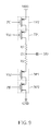
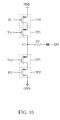
- FIG.9 and FIG.10 are examples for the driving circuit illustrated in FIG.2 .
- the driving circuit further comprises resistors R1 and R2, which are coupled in series and coupled to the input/output pad I/O.
- the driving circuit comprises a resistor R3 coupled between the output terminal OT and the input/output pad I/O. Such variation should also fall in the scope of the present application.
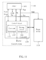
- the control system 1100 comprises a power managing IC (integrated circuit) 1101 and a control IC 1103.
- the power managing IC 1101 comprises a power providing terminal Tpp for providing a predetermined voltage VDD.
- the control IC 1103, which is applied to control a target device 1111 comprises: a power receiving terminal Tpr for receiving the predetermined voltage VDD; and a bias voltage receiving terminal Tbr, for receiving a bias voltage Vb generated from at least operating voltage of the control IC 1103.
- the bias voltage Vb is applied to bias at least one transistor (ex. the transistor Tp1 in FIG.2 ) in the control IC 1103.
- the control IC 1103 comprises a control circuit 1105, which may comprise the same structure as which of the control circuit 200 in FIG.2 . Accordingly, the control circuit 1105 receives the bias voltage Vb from the bias voltage receiving terminal Tbr and receives the predetermined voltage VDD from the power receiving terminal Tpr.
- the control circuit 1105 can comprise a core unit 1107 (ex. a DRAM controller) and a driving circuit 1109, the same as the control circuit in FIG.2 .
- the core unit 1107 can be the same as the core unit 201 in FIG.2
- the driving circuit 1107 can comprise a structure the same as which of the driving circuit 203 in FIG.2 , but not limited.
- control IC 1103 can further comprise a core voltage receiving terminal Tcore to receive a core voltage Vcore from the power managing IC 1101 and transmits the core voltage Vcore to the control circuit 1105. Please note if the control IC 1103 does not comprise the core unit 1107, the core voltage receiving terminal Tcore can be omitted.
- the control IC 1103 receives the bias voltage Vb from the power managing IC 1101 (ex. the embodiment in FIG.5 ).
- the bias voltage Vb can equal to the core voltage Vcore or the predetermined voltage minus the core voltage VDD-Vcore.
- the control IC 1103 does not directly receive the bias voltage Vb from the power managing IC 1101.
- the power managing IC 1101 provides the core voltage Vcore to either the core unit 1107 or the driving circuit 1109 via the core voltage receiving terminal Tcore.
- the bias voltage can equal to the core voltage Vcore or the predetermined voltage minus the core voltage VDD-Vcore (ex. the embodiment in FIG.3A or FIG.3B ) .
- the core voltage receiving terminal Tcore can be regarded as a bias voltage receiving terminal.
- a bias generating circuit such as 301 in FIG.3A is needed.
- the control IC 1103 does not receive the bias voltage Vb from the power managing IC 1101.
- the power managing IC 1101 provides the core voltage Vcore to the core unit 1107 but not to the driving circuit 1109.
- the driving circuit 1109 receives the core voltage Vcore from the core unit 201 if needed.
- the bias voltage can equal to the core voltage Vcore or the predetermined voltage minus the core voltage VDD-Vcore (ex. the embodiment in FIG.3A or FIG.3B ).
- the core voltage Vcore is directly applied as the bias voltage from the core unit 1107.
- a bias generating circuit such as 301 in FIG.3A is needed.
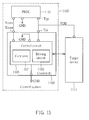
- the bias voltage receiving terminal Tbr can be coupled to a ground voltage source providing the ground voltage.
- the control system 1100 is provided on a circuit board, and the ground voltage source is located on the circuit board, as shown in FIG.14 .
- the driving circuit 1109 is provided in a silicon die, and the control IC 1103 is comprised in a package comprising the silicon die, the power receiving terminal Tpr and the bias voltage receiving terminal Tb.
- the ground voltage source can be located in the package and outside the silicon die, as shown in FIG.15 .
- the ground voltage source can be located in the silicon die, as shown in FIG.16 .
- FIG.11-FIG.16 can be applied to a 1.2v CMOS logic device, following JESD 76-1 spec, or HSIC USB 2.0 spec, but not limited.
- the driving circuit, the control circuit and the control system can provide bias voltages meeting different requirements, thus the applicability of the driving circuit, the control circuit and the control system is extended.
Landscapes
- Engineering & Computer Science (AREA)
- Theoretical Computer Science (AREA)
- Physics & Mathematics (AREA)
- General Physics & Mathematics (AREA)
- General Engineering & Computer Science (AREA)
- Electromagnetism (AREA)
- Radar, Positioning & Navigation (AREA)
- Automation & Control Theory (AREA)
- Semiconductor Integrated Circuits (AREA)
- Logic Circuits (AREA)
- Electronic Switches (AREA)
Abstract
Description
- The present application relates to a control circuit and a control system, and particularly relates to a control circuit and a control system that can apply different bias voltages corresponding to different standards.
- The present application relates to a control circuit and a control system, and particularly relates to a control circuit and a control system that can provide different bias voltages for a driving circuit included therein.
-
FIG.1 is a circuit diagram illustrating aconventional driving circuit 100. As illustrated inFIG.1 , thedriving circuit 100 comprises transistors TP1, TP2, TN1 and TN2, which are coupled in series and coupled to an input/output pad I/O. The transistor TP2 receives a pull up signal PU. If the pull up signal PU controls the transistor TP2 to be active, a voltage at the output terminal OT is pulled up. The transistor TP1 receives a bias voltage Vb1 to operate in a suitable state. - Similarly, the transistor TN2 receives a pull down signal PD. If the pull down signal PD controls the transistor TN2 to be active, a voltage at the output terminal OT is pulled down. The transistor TN1 receives a bias voltage Vb2 to operate in a suitable state.
- However, the bias voltage Vb1 or Vb2 must be provided by another independent bias voltage source which may occupy more circuit regions. Also, the bias voltage is always a fixed value thus cannot meet different requirements.
- This in mind, the present application aims at providing a control circuit that can provide different bias voltages to a driving circuit included therein.
- Further, the present application also aims at providing a control system that can provide different bias voltages to a control IC included therein.
- This is achieved by a control circuit according to
claim 1 and control systems according to claims 6 and 13. The dependent claims pertain to corresponding further developments and improvements. - As will be seen more clearly from the detailed description following below, the claimed control circuit comprising a driving circuit which comprises a voltage adjusting circuit, a first transistor and a second transistor. The first transistor comprises: a first terminal; a second terminal; and a control terminal, for receiving a bias voltage generated from at least operating voltage of the control circuit. The second transistor comprises: a first terminal, coupled to a second terminal of the first transistor; a second terminal, for receiving a first predetermined voltage; and a control terminal, for receiving the control voltage.
- Also, a claimed control system comprises a power managing IC, and a control IC. The power managing IC comprises a power providing terminal for providing a first predetermined voltage. The control IC comprises: at least one transistor; a power receiving terminal, for receiving the first predetermined voltage; and a bias voltage receiving terminal, for receiving a bias voltage generated from at least operating voltage of the control IC, wherein the bias voltage is applied to bias at least one transistor in the control IC.
- Furthermore, a claimed control system comprising a power managing IC and a control IC. The power managing IC comprises a power providing terminal for providing a first predetermined voltage. The control IC comprises: at least one transistor; a power receiving terminal , for receiving the first predetermined voltage; a core voltage receiving terminal, for receiving a core voltage; a core unit, receiving the core voltage; and a bias voltage generating circuit, for generating a bias voltage applied to bias the transistor in the control IC according to the core voltage. The bias voltage equals to the first predetermined voltage minus the core voltage.
- These and other objectives of the present invention will no doubt become obvious to those of ordinary skill in the art after reading the following detailed description of the preferred embodiment that is illustrated in the various figures and drawings.
- In the following, the invention is further illustrated by way of example, taking reference to the accompanying drawings. Thereof
-
FIG.1 is a circuit diagram illustrating a conventional driving circuit; -
FIG.2 is a circuit diagram illustrating a control circuit according to one embodiment of the present application; -
FIG.3A ,FIG.3B ,FIG.4-FIG.8 are circuit diagrams illustrating different examples for the embodiment illustrated inFIG.2 ; -
FIG.9 andFIG.10 are examples for the driving circuit illustrated inFIG.2 ; and -
FIG.11-FIG.16 are block diagrams illustrating the control system according to embodiments of the present application. -
FIG.2 is a circuit diagram illustrating acontrol circuit 200 according to one embodiment of the present application. As illustrated inFIG.2 , thecontrol circuit 200 comprises acore unit 201 and a driving circuit-205. Thecore unit 201, which receives and operates at a core voltage Vcore, is a device for higher speed operations and lower voltage operations. Accordingly, the core device can be applied as a circuit providing more functions, such as a controller. Comparing with an I/O (input/output) device applied for the input/output pad, the core unit has thinner oxides. - The
driving circuit 203 is a pull up module in this example, which comprises a pull up circuit PUC (i.e. a voltage adjusting circuit) for generating a control voltage CV (i.e. the pull up signal PU inFIG.1 ), a transistor TP1 and a transistor TP2. The transistor TP1 and the transistor TP2 are PMOSFETs in this example. The transistor TP1 comprises: a first terminal (drain terminal) coupled to the input/output pad I/O; a second terminal (source terminal); and a control terminal (gate terminal) for receiving a bias voltage Vb generated from at least operating voltage of thecontrol circuit 200. The transistor TP2 comprises: a first terminal (drain terminal), coupled to a second terminal of the first transistor TP1; a second terminal (source terminal), for receiving a predetermined voltage VDD; and a control terminal (gate terminal), for receiving the control voltage CV. - In one embodiment, the predetermined voltage VDD meets one of following specs: DDR3, DDR3L, LPDDR3, DDR4, LPDDR4, GPIO. Corresponding to the spec, a value of the bias voltage Vb can equal to the core voltage Vcore, the predetermined voltage minus the core voltage VDD-Vcore, or a ground voltage GND. Please note either the core voltage Vcore, the predetermined voltage minus the core voltage VDD-Vcore or the ground voltage GND is an operating voltage of the
control circuit 200. Accordingly, the bias voltage Vb is generated from the operating voltages of thecontrol circuit 200. - The following table T1 depicts the examples of the predetermined voltage VDD and the bias voltage Vb corresponding to different specs. However, these values are only examples and do not mean to limit the scope of the present application.
T1 VDD Vb Spec 1.5V VDD-Vcore DDR3 1. 35V VDD-Vcore or GND DDR3L 1.2V GND LPDDR3/DDR4 1.1V GND LPDDR4 1.8V Vcore GPIO - In this embodiment, the
control circuit 200 further comprises a pull downmodule 205 , which can be regarded as a driving circuit as well, comprising a pull down circuit PDC, which is also as a voltage adjusting circuit, a transistor TN1 and a transistor TN2. The transistor TN1 and the transistor TN2 are NMOSFETs in this embodiment. Please note, in one embodiment, the transistor TN1 receives the core voltage Vcore for biasing. However, if the concept of thedriving circuit 203 is applied to the pull downmodule 205. The voltage received by the control terminal of the transistor TN1 is replaced by a bias voltage generated from the operating voltages of thecontrol circuit 200. In other embodiments, thedriving circuit 203 may further comprise other circuits such as a level shifter or a buffer located between thecore unit 201 and the pull up circuit PUC, or the pull downmodule 205 comprises other circuits such as a level shifter or a buffer located between thecore unit 201 and the pull down circuit PDC. Such variation should also fall in the scope of the present application. - Please note, the
driving circuit 203 is not limited to be applied to the control circuit illustrated inFIG.2 . Accordingly, a driving circuit provided by the present application can be summarized as: A driving circuit, comprising a voltage adjusting circuit (ex. the pull up circuit PUC for a pull upmodule 203, or the pull down circuit PDC for the pull down module 205) for generating a control voltage CV, comprising a first transistor (ex. the transistor TP1 for a pull up module , or the transistor TN1 for the pull down module 205) and a second transistor (ex. the transistor TP2 for a pull up module , or the transistor TN2 for the pull down module 205). The first transistor comprises: a first terminal; a second terminal; and a control terminal, for receiving a bias voltage (ex.Vb) generated from at least operating voltage of the control circuit. The second transistor comprises: a first terminal, coupled to a second terminal of the first transistor; a second terminal, for receiving a predetermined voltage (ex. VDD); and a control terminal, for receiving the control voltage (ex. CV). -
FIG.3A ,FIG.3B ,FIG.4-FIG.8 are circuit diagrams illustrating different examples for the embodiment illustrated inFIG. 2 . These examples illustrate how to provide required bias voltages. In the example ofFIG.3A , a biasvoltage generating circuit 301 is provided in thedriving circuit 203. The biasing circuit receives the predetermined voltage VDD and the core voltage Vcore to generate a voltage equaling to the predetermined voltage minus the core voltage VDD-Vcore as a bias voltage Vb. The core voltage Vcore can come from thecore unit 201 or an external source outside thecontrol circuit 200. Please note the biasvoltage generating circuit 301 can be incorporated into the pull up circuit PUC (i.e. the voltage adjusting circuit), as shown inFIG.3B . The structure inFIG. 3B can also provide a bias voltage Vb equaling to the core voltage Vcore. Please note if the bias voltage Vb equals to the core voltage Vcore, it can be directly from the core unit,as illustrated inFIG.4 . - In the embodiment of
FIG.5 , the bias voltage Vb is from an external source outside thecontrol circuit 200, which will be described later. In such case, the bias voltage can equal to the ground voltage GND or VDD-Vcore. In the embodiment ofFIG.6 , the bias voltage Vb equals to a ground voltage GND, and the pull up circuit PUC is also coupled to the ground voltage GND. In the embodiment ofFIG.7 , amultiplexer 701 is further provided in thedriving circuit 203 to select a required bias voltage from a plurality of candidate voltages. In this example, candidate voltages are the ground voltage GND and the core voltage Vcore, but not limited. - Further, in the embodiment of
FIG.8 , the driving circuit further comprises amultiplexer 801 and a candidatevoltage selecting circuit 803. The candidatevoltage selecting circuit 803 outputs one of a plurality of candidate voltages (in this example, the core voltage Vcore, and the predetermined voltage minus the core voltage VDD-Vcore). Themultiplexer 801 outputs the candidate voltage output from the candidatevoltage selecting circuit 803 and a second predetermined voltage (the ground voltage GND in this example) as the bias voltage Vb. It will be appreciated that the candidate voltages are also related with the operating voltage of the control circuit. - The structure for the driving circuit is not limited to above-mentioned embodiments.
FIG.9 andFIG.10 are examples for the driving circuit illustrated inFIG.2 . As shown inFIG.9 , the driving circuit further comprises resistors R1 and R2, which are coupled in series and coupled to the input/output pad I/O. In the example ofFIG.10 , the driving circuit comprises a resistor R3 coupled between the output terminal OT and the input/output pad I/O. Such variation should also fall in the scope of the present application. - The following embodiments will depict the above-mentioned embodiments in a system view. As illustrated in
FIG.11 , thecontrol system 1100 comprises a power managing IC (integrated circuit) 1101 and acontrol IC 1103. Thepower managing IC 1101 comprises a power providing terminal Tpp for providing a predetermined voltage VDD. Thecontrol IC 1103, which is applied to control a target device 1111 (ex. a DRAM die), comprises: a power receiving terminal Tpr for receiving the predetermined voltage VDD; and a bias voltage receiving terminal Tbr, for receiving a bias voltage Vb generated from at least operating voltage of thecontrol IC 1103. The bias voltage Vb is applied to bias at least one transistor (ex. the transistor Tp1 inFIG.2 ) in thecontrol IC 1103. - In one embodiment, the
control IC 1103 comprises acontrol circuit 1105, which may comprise the same structure as which of thecontrol circuit 200 inFIG.2 . Accordingly, thecontrol circuit 1105 receives the bias voltage Vb from the bias voltage receiving terminal Tbr and receives the predetermined voltage VDD from the power receiving terminal Tpr. In such embodiment, thecontrol circuit 1105 can comprise a core unit 1107 (ex. a DRAM controller) and adriving circuit 1109, the same as the control circuit inFIG.2 . Thecore unit 1107 can be the same as thecore unit 201 inFIG.2 , and thedriving circuit 1107 can comprise a structure the same as which of the drivingcircuit 203 inFIG.2 , but not limited. Also, thecontrol IC 1103 can further comprise a core voltage receiving terminal Tcore to receive a core voltage Vcore from thepower managing IC 1101 and transmits the core voltage Vcore to thecontrol circuit 1105. Please note if thecontrol IC 1103 does not comprise thecore unit 1107, the core voltage receiving terminal Tcore can be omitted. - In the embodiment of
FIG. 11 , thecontrol IC 1103 receives the bias voltage Vb from the power managing IC 1101 (ex. the embodiment inFIG.5 ). In such case, the bias voltage Vb can equal to the core voltage Vcore or the predetermined voltage minus the core voltage VDD-Vcore. - In the embodiment of
FIG. 12 , thecontrol IC 1103 does not directly receive the bias voltage Vb from thepower managing IC 1101. Thepower managing IC 1101 provides the core voltage Vcore to either thecore unit 1107 or thedriving circuit 1109 via the core voltage receiving terminal Tcore. In such case, the bias voltage can equal to the core voltage Vcore or the predetermined voltage minus the core voltage VDD-Vcore (ex. the embodiment inFIG.3A orFIG.3B ) . In the case that the bias voltage equals to the core voltage Vcore(ex. the embodiment inFIG.5 ), the core voltage receiving terminal Tcore can be regarded as a bias voltage receiving terminal. However, in the case that the bias voltage equals to the predetermined voltage minus the core voltage VDD-Vcore, a bias generating circuit such as 301 inFIG.3A is needed. - In the embodiment of
FIG.13 , thecontrol IC 1103 does not receive the bias voltage Vb from thepower managing IC 1101. Thepower managing IC 1101 provides the core voltage Vcore to thecore unit 1107 but not to thedriving circuit 1109. In such case, thedriving circuit 1109 receives the core voltage Vcore from thecore unit 201 if needed. Also, the bias voltage can equal to the core voltage Vcore or the predetermined voltage minus the core voltage VDD-Vcore (ex. the embodiment inFIG.3A orFIG.3B ). In the case that the bias voltage equals to the core voltage Vcore, the core voltage Vcore is directly applied as the bias voltage from thecore unit 1107. However, in the case that the bias voltage equals to the predetermined voltage minus the core voltage VDD-Vcore, a bias generating circuit such as 301 inFIG.3A is needed. - If the bias voltage equals to a ground voltage GND, the bias voltage receiving terminal Tbr can be coupled to a ground voltage source providing the ground voltage. In one embodiment, the
control system 1100 is provided on a circuit board, and the ground voltage source is located on the circuit board, as shown inFIG.14 . Also, in one embodiment, thedriving circuit 1109 is provided in a silicon die, and thecontrol IC 1103 is comprised in a package comprising the silicon die, the power receiving terminal Tpr and the bias voltage receiving terminal Tb. In such case, the ground voltage source can be located in the package and outside the silicon die, as shown inFIG.15 . Alternatively, the ground voltage source can be located in the silicon die, as shown inFIG.16 . - The embodiments in
FIG.11-FIG.16 can be applied to a 1.2v CMOS logic device, following JESD 76-1 spec, or HSIC USB 2.0 spec, but not limited. - In view of above-mentioned embodiments, the driving circuit, the control circuit and the control system can provide bias voltages meeting different requirements, thus the applicability of the driving circuit, the control circuit and the control system is extended.
- Those skilled in the art will readily observe that numerous modifications and alterations of the device and method may be made while retaining the teachings of the invention. Accordingly, the above disclosure should be construed as limited only by the metes and bounds of the appended claims.
Claims (15)
- A control circuit (200), characterized by comprising:a driving circuit (203, 205), comprising a voltage adjusting circuit (PUC) for generating a control voltage, comprising a first transistor (TP1. TN1) and a second transistor (TP2, TN2);wherein the first transistor comprises:a first terminal;a second terminal; anda control terminal, for receiving a bias voltage (Vb) generated from at least operating voltage of the control circuit ;wherein the second transistor comprises:a first terminal, coupled to a second terminal of the first transistor;a second terminal, for receiving a first predetermined voltage; anda control terminal, for receiving the control voltage.
- The control circuit of claim 1, further characterized by comprising:a candidate voltage selecting circuit (803), for outputting one of a plurality of candidate voltages; anda multiplexer (801), for outputting one of the candidate voltage output from the candidate voltage selecting circuit and a ground voltage as the bias voltage;wherein the candidate voltages are related with the operating voltage of the control circuit.
- The control circuit of claim 1, further characterized by comprising a core unit (201) receiving a core voltage (Vcore), wherein the bias voltage equals to the first predetermined voltage minus the core voltage.
- The control circuit of claim 3, further characterized by comprising a bias voltage generating circuit (301, PUC), wherein the bias voltage generating circuit receives the core voltage thereby the bias voltage generating circuit generates the bias voltage according to the core voltage.
- The control circuit of claim 1, characterized by, wherein the control circuit further comprises a core unit (201)receiving a core voltage (Vcore), wherein the bias voltage equals to the core voltage.
- A control system (1100), characterized by comprising:a power managing IC (1101) (integrated circuit), comprising a power providing terminal for providing a first predetermined voltage; anda control IC (1105), comprising:at least one transistor;a power receiving terminal (Tpr), for receiving the first predetermined voltage; anda bias voltage receiving terminal (Tbr), for receiving a bias voltage generated from at least operating voltage of the control IC, wherein the bias voltage is applied to bias at least one transistor in the control IC.
- The control system of claim 6, characterized by, wherein the control IC comprises:a voltage adjusting circuit (PUC), for generating a control voltage;a first transistor (TP1), applied as the transistor, comprising:a first terminal;a second terminal; anda control terminal, for receiving the bias voltage (Vb);anda second transistor (TP2), comprising:a first terminal, coupled to a second terminal of the first transistor;a second terminal, for receiving the first predetermined voltage (VDD); anda control terminal, for receiving the control voltage.
- The control system of claim 6, characterized by, wherein the control IC further comprises a core unit (1107) receiving a core voltage (Vcore)from the bias voltage receiving terminal, wherein the bias voltage equals to the core voltage.
- The control system of claim 8, characterized by, wherein the power managing IC provides the core voltage to the core unit via the bias voltage receiving terminal, and the core unit provides the core voltage as the bias voltage.
- The control system of claim 6, characterized by, wherein the bias voltage is a ground voltage, wherein the control system is provided on a circuit board, wherein a ground voltage source providing the ground voltage is located on the circuit board.
- The control system of claim 6, characterized by, wherein the bias voltage is a ground voltage, wherein the control IC comprises:a silicon die, wherein the transistor is provided in the silicon die; anda package, comprising the silicon die, the power receiving terminal, and the bias voltage receiving terminal;wherein a ground voltage source providing the ground voltage is located in the package and outside the silicon die.
- The control system of claim 6, characterized by, wherein the bias voltage is a ground voltage, wherein the control IC comprises:a silicon die, wherein the transistor is provided in the silicon die; anda package, comprising the silicon die, the power receiving terminal, and the bias voltage receiving terminal;wherein a ground voltage source providing the ground voltage is located in the silicon die.
- A control system (1100), characterized by comprising:a power managing IC (1101) (integrated circuit), comprising a power providing terminal for providing a first predetermined voltage; anda control IC (1103), comprising:at least one transistor;a power receiving terminal (Tpr), for receiving the first predetermined voltage;a core voltage receiving terminal (Tcore), for receiving a core voltage;a core unit (1107), receiving the core voltage; anda bias voltage generating circuit (301, PUC), for generating a bias voltage applied to bias the transistor in the control IC according to the core voltage;wherein the bias voltage equals to the first predetermined voltage minus the core voltage.
- The control system of claim 13, characterized by, wherein the power managing IC provides the core voltage to the core unit and the control IC via the core voltage receiving terminal, thereby the bias voltage generating circuit generates the bias voltage according to the core voltage.
- The control system of claim 13, characterized by, wherein the power managing IC provides the core voltage to the core unit via the core voltage receiving terminal, wherein the core unit outputs the core voltage thereby the bias voltage generating circuit generate the bias voltage according to the core voltage.
Applications Claiming Priority (2)
| Application Number | Priority Date | Filing Date | Title |
|---|---|---|---|
| US201462001640P | 2014-05-22 | 2014-05-22 | |
| US14/599,553 US9746866B2 (en) | 2014-05-22 | 2015-01-19 | Control circuit and control system |
Publications (3)
| Publication Number | Publication Date |
|---|---|
| EP2957985A2 true EP2957985A2 (en) | 2015-12-23 |
| EP2957985A3 EP2957985A3 (en) | 2016-03-23 |
| EP2957985B1 EP2957985B1 (en) | 2017-06-07 |
Family
ID=53180512
Family Applications (1)
| Application Number | Title | Priority Date | Filing Date |
|---|---|---|---|
| EP15164206.3A Active EP2957985B1 (en) | 2014-05-22 | 2015-04-20 | Control circuit and control system |
Country Status (3)
| Country | Link |
|---|---|
| US (2) | US9746866B2 (en) |
| EP (1) | EP2957985B1 (en) |
| CN (1) | CN105099141B (en) |
Cited By (1)
| Publication number | Priority date | Publication date | Assignee | Title |
|---|---|---|---|---|
| CN114115411A (en) * | 2021-05-12 | 2022-03-01 | 友达光电股份有限公司 | Voltage modulation circuit and operation method thereof |
Families Citing this family (3)
| Publication number | Priority date | Publication date | Assignee | Title |
|---|---|---|---|---|
| CN106027012B (en) * | 2016-06-13 | 2023-05-05 | 达凯(上海)电子科技有限公司 | Pull-down resistor switch circuit |
| US10715139B2 (en) | 2018-08-29 | 2020-07-14 | Advanced Micro Devices, Inc. | Gate-source voltage generation for pull-up and pull-down devices in I/O designs |
| US11855631B2 (en) * | 2020-08-19 | 2023-12-26 | Montage Technology Co., Ltd. | Asymmetrical I/O structure |
Family Cites Families (14)
| Publication number | Priority date | Publication date | Assignee | Title |
|---|---|---|---|---|
| US6847248B2 (en) * | 2001-01-09 | 2005-01-25 | Broadcom Corporation | Sub-micron high input voltage tolerant input output (I/O) circuit which accommodates large power supply variations |
| US7605611B2 (en) | 2007-10-24 | 2009-10-20 | Micron Technology, Inc. | Methods, devices, and systems for a high voltage tolerant buffer |
| US8344760B2 (en) * | 2008-07-17 | 2013-01-01 | Ati Technologies Ulc | Input/output buffer circuit |
| US8026745B2 (en) | 2009-03-16 | 2011-09-27 | Apple Inc. | Input/output driver with controlled transistor voltages |
| US8406354B2 (en) | 2009-07-01 | 2013-03-26 | Telefonaktiebolaget L M Ericsson (Publ) | Interference cancellation in a multi-user receiver |
| US20110316505A1 (en) * | 2010-06-23 | 2011-12-29 | Texas Instruments Incorporated | Output Buffer With Improved Output Signal Quality |
| KR101825114B1 (en) * | 2011-11-07 | 2018-03-14 | 삼성전자주식회사 | Output buffer, operating method thereof, and devices having the same |
| US8476940B2 (en) * | 2011-12-02 | 2013-07-02 | Stmicroelectronics International N.V. | Stress reduced cascoded CMOS output driver circuit |
| FR2984645B1 (en) | 2011-12-20 | 2014-11-21 | Thales Sa | METHOD FOR RETRANSMITTING FRAGMENTED PACKETS |
| US8896147B2 (en) | 2011-12-23 | 2014-11-25 | Ati Technologies Ulc | Low power implementation to allow for high potential rails to come up in any order |
| JP2013192110A (en) | 2012-03-14 | 2013-09-26 | Mitsumi Electric Co Ltd | Bias voltage generation circuit and differential circuit |
| KR101989571B1 (en) | 2012-06-27 | 2019-06-14 | 삼성전자주식회사 | output driver for high voltage and wide range voltage operation and data output driving circuit using the same |
| US9213382B2 (en) * | 2012-09-12 | 2015-12-15 | Intel Corporation | Linear voltage regulator based on-die grid |
| WO2015047276A1 (en) * | 2013-09-26 | 2015-04-02 | Intel Corporation | Low dropout voltage regulator integrated with digital power gate driver |
-
2015
- 2015-01-19 US US14/599,553 patent/US9746866B2/en active Active
- 2015-04-20 EP EP15164206.3A patent/EP2957985B1/en active Active
- 2015-05-14 CN CN201510245169.8A patent/CN105099141B/en active Active
-
2017
- 2017-07-19 US US15/654,694 patent/US9798345B1/en active Active
Non-Patent Citations (1)
| Title |
|---|
| None |
Cited By (2)
| Publication number | Priority date | Publication date | Assignee | Title |
|---|---|---|---|---|
| CN114115411A (en) * | 2021-05-12 | 2022-03-01 | 友达光电股份有限公司 | Voltage modulation circuit and operation method thereof |
| CN114115411B (en) * | 2021-05-12 | 2023-02-28 | 友达光电股份有限公司 | Voltage modulation circuit and operation method thereof |
Also Published As
| Publication number | Publication date |
|---|---|
| CN105099141B (en) | 2018-03-09 |
| US9746866B2 (en) | 2017-08-29 |
| EP2957985A3 (en) | 2016-03-23 |
| US9798345B1 (en) | 2017-10-24 |
| US20150338870A1 (en) | 2015-11-26 |
| US20170315577A1 (en) | 2017-11-02 |
| EP2957985B1 (en) | 2017-06-07 |
| CN105099141A (en) | 2015-11-25 |
Similar Documents
| Publication | Publication Date | Title |
|---|---|---|
| US9136827B2 (en) | Power-on reset circuit | |
| US9798345B1 (en) | Control circuit and control system | |
| JP2006039788A (en) | Semiconductor integrated circuit device | |
| JP2017215906A (en) | Series regulator and semiconductor integrated circuit | |
| US9819332B2 (en) | Circuit for reducing negative glitches in voltage regulator | |
| US9337842B1 (en) | Low voltage differential signaling (LVDS) driving circuit | |
| KR20110005792A (en) | High Voltage Immunity Input / Output Interface Circuit | |
| US9454165B2 (en) | Semiconductor device and current control method that controls amount of current used for voltage generation based on connection state of external capacitor | |
| US8957708B2 (en) | Output buffer and semiconductor device | |
| US9018986B2 (en) | Output buffers | |
| US6621329B2 (en) | Semiconductor device | |
| CN109964276B (en) | Circuitry for Bleeding Supply Voltage from Devices in Power-Down State | |
| US7449952B2 (en) | Amplifying circuit having a pull-up circuit and a pull-down circuit for increasing slew rate | |
| JP5522705B2 (en) | Semiconductor device | |
| JP5419111B2 (en) | Semiconductor device | |
| US7262646B2 (en) | Power-on reset circuit | |
| US8723581B1 (en) | Input buffers | |
| JP5838845B2 (en) | Semiconductor integrated circuit | |
| US7652530B2 (en) | Amplifier circuit and method of generating bias voltage in amplifier circuit | |
| JP4578882B2 (en) | Semiconductor integrated circuit | |
| US20150095668A1 (en) | Internal voltage generation circuits | |
| JP4147174B2 (en) | Power-on reset circuit | |
| US8446182B2 (en) | TX output combining method between different bands | |
| US20130321060A1 (en) | Input buffer circuit and semiconductor device | |
| KR20120018453A (en) | Input buffer of a semiconductor memory apparatus |
Legal Events
| Date | Code | Title | Description |
|---|---|---|---|
| PUAI | Public reference made under article 153(3) epc to a published international application that has entered the european phase |
Free format text: ORIGINAL CODE: 0009012 |
|
| AK | Designated contracting states |
Kind code of ref document: A2 Designated state(s): AL AT BE BG CH CY CZ DE DK EE ES FI FR GB GR HR HU IE IS IT LI LT LU LV MC MK MT NL NO PL PT RO RS SE SI SK SM TR |
|
| AX | Request for extension of the european patent |
Extension state: BA ME |
|
| PUAL | Search report despatched |
Free format text: ORIGINAL CODE: 0009013 |
|
| AK | Designated contracting states |
Kind code of ref document: A3 Designated state(s): AL AT BE BG CH CY CZ DE DK EE ES FI FR GB GR HR HU IE IS IT LI LT LU LV MC MK MT NL NO PL PT RO RS SE SI SK SM TR |
|
| AX | Request for extension of the european patent |
Extension state: BA ME |
|
| RIC1 | Information provided on ipc code assigned before grant |
Ipc: G06F 1/26 20060101ALI20160212BHEP Ipc: G06F 1/32 20060101AFI20160212BHEP |
|
| 17P | Request for examination filed |
Effective date: 20160503 |
|
| RBV | Designated contracting states (corrected) |
Designated state(s): AL AT BE BG CH CY CZ DE DK EE ES FI FR GB GR HR HU IE IS IT LI LT LU LV MC MK MT NL NO PL PT RO RS SE SI SK SM TR |
|
| 17Q | First examination report despatched |
Effective date: 20160805 |
|
| GRAP | Despatch of communication of intention to grant a patent |
Free format text: ORIGINAL CODE: EPIDOSNIGR1 |
|
| RIC1 | Information provided on ipc code assigned before grant |
Ipc: G06F 1/32 20060101AFI20170203BHEP Ipc: G06F 1/26 20060101ALI20170203BHEP Ipc: G05F 3/02 20060101ALI20170203BHEP |
|
| INTG | Intention to grant announced |
Effective date: 20170227 |
|
| GRAS | Grant fee paid |
Free format text: ORIGINAL CODE: EPIDOSNIGR3 |
|
| AK | Designated contracting states |
Kind code of ref document: B1 Designated state(s): AL AT BE BG CH CY CZ DE DK EE ES FI FR GB GR HR HU IE IS IT LI LT LU LV MC MK MT NL NO PL PT RO RS SE SI SK SM TR |
|
| REG | Reference to a national code |
Ref country code: GB Ref legal event code: FG4D |
|
| GRAA | (expected) grant |
Free format text: ORIGINAL CODE: 0009210 |
|
| REG | Reference to a national code |
Ref country code: CH Ref legal event code: EP Ref country code: AT Ref legal event code: REF Ref document number: 899680 Country of ref document: AT Kind code of ref document: T Effective date: 20170615 |
|
| REG | Reference to a national code |
Ref country code: IE Ref legal event code: FG4D |
|
| REG | Reference to a national code |
Ref country code: DE Ref legal event code: R096 Ref document number: 602015002966 Country of ref document: DE |
|
| REG | Reference to a national code |
Ref country code: NL Ref legal event code: MP Effective date: 20170607 |
|
| REG | Reference to a national code |
Ref country code: LT Ref legal event code: MG4D |
|
| PG25 | Lapsed in a contracting state [announced via postgrant information from national office to epo] |
Ref country code: GR Free format text: LAPSE BECAUSE OF FAILURE TO SUBMIT A TRANSLATION OF THE DESCRIPTION OR TO PAY THE FEE WITHIN THE PRESCRIBED TIME-LIMIT Effective date: 20170908 Ref country code: NO Free format text: LAPSE BECAUSE OF FAILURE TO SUBMIT A TRANSLATION OF THE DESCRIPTION OR TO PAY THE FEE WITHIN THE PRESCRIBED TIME-LIMIT Effective date: 20170907 Ref country code: ES Free format text: LAPSE BECAUSE OF FAILURE TO SUBMIT A TRANSLATION OF THE DESCRIPTION OR TO PAY THE FEE WITHIN THE PRESCRIBED TIME-LIMIT Effective date: 20170607 Ref country code: LT Free format text: LAPSE BECAUSE OF FAILURE TO SUBMIT A TRANSLATION OF THE DESCRIPTION OR TO PAY THE FEE WITHIN THE PRESCRIBED TIME-LIMIT Effective date: 20170607 Ref country code: FI Free format text: LAPSE BECAUSE OF FAILURE TO SUBMIT A TRANSLATION OF THE DESCRIPTION OR TO PAY THE FEE WITHIN THE PRESCRIBED TIME-LIMIT Effective date: 20170607 Ref country code: HR Free format text: LAPSE BECAUSE OF FAILURE TO SUBMIT A TRANSLATION OF THE DESCRIPTION OR TO PAY THE FEE WITHIN THE PRESCRIBED TIME-LIMIT Effective date: 20170607 |
|
| REG | Reference to a national code |
Ref country code: AT Ref legal event code: MK05 Ref document number: 899680 Country of ref document: AT Kind code of ref document: T Effective date: 20170607 |
|
| PG25 | Lapsed in a contracting state [announced via postgrant information from national office to epo] |
Ref country code: RS Free format text: LAPSE BECAUSE OF FAILURE TO SUBMIT A TRANSLATION OF THE DESCRIPTION OR TO PAY THE FEE WITHIN THE PRESCRIBED TIME-LIMIT Effective date: 20170607 Ref country code: SE Free format text: LAPSE BECAUSE OF FAILURE TO SUBMIT A TRANSLATION OF THE DESCRIPTION OR TO PAY THE FEE WITHIN THE PRESCRIBED TIME-LIMIT Effective date: 20170607 Ref country code: NL Free format text: LAPSE BECAUSE OF FAILURE TO SUBMIT A TRANSLATION OF THE DESCRIPTION OR TO PAY THE FEE WITHIN THE PRESCRIBED TIME-LIMIT Effective date: 20170607 Ref country code: LV Free format text: LAPSE BECAUSE OF FAILURE TO SUBMIT A TRANSLATION OF THE DESCRIPTION OR TO PAY THE FEE WITHIN THE PRESCRIBED TIME-LIMIT Effective date: 20170607 Ref country code: BG Free format text: LAPSE BECAUSE OF FAILURE TO SUBMIT A TRANSLATION OF THE DESCRIPTION OR TO PAY THE FEE WITHIN THE PRESCRIBED TIME-LIMIT Effective date: 20170907 |
|
| PG25 | Lapsed in a contracting state [announced via postgrant information from national office to epo] |
Ref country code: AT Free format text: LAPSE BECAUSE OF FAILURE TO SUBMIT A TRANSLATION OF THE DESCRIPTION OR TO PAY THE FEE WITHIN THE PRESCRIBED TIME-LIMIT Effective date: 20170607 Ref country code: SK Free format text: LAPSE BECAUSE OF FAILURE TO SUBMIT A TRANSLATION OF THE DESCRIPTION OR TO PAY THE FEE WITHIN THE PRESCRIBED TIME-LIMIT Effective date: 20170607 Ref country code: RO Free format text: LAPSE BECAUSE OF FAILURE TO SUBMIT A TRANSLATION OF THE DESCRIPTION OR TO PAY THE FEE WITHIN THE PRESCRIBED TIME-LIMIT Effective date: 20170607 Ref country code: CZ Free format text: LAPSE BECAUSE OF FAILURE TO SUBMIT A TRANSLATION OF THE DESCRIPTION OR TO PAY THE FEE WITHIN THE PRESCRIBED TIME-LIMIT Effective date: 20170607 Ref country code: EE Free format text: LAPSE BECAUSE OF FAILURE TO SUBMIT A TRANSLATION OF THE DESCRIPTION OR TO PAY THE FEE WITHIN THE PRESCRIBED TIME-LIMIT Effective date: 20170607 |
|
| PG25 | Lapsed in a contracting state [announced via postgrant information from national office to epo] |
Ref country code: IS Free format text: LAPSE BECAUSE OF FAILURE TO SUBMIT A TRANSLATION OF THE DESCRIPTION OR TO PAY THE FEE WITHIN THE PRESCRIBED TIME-LIMIT Effective date: 20171007 Ref country code: IT Free format text: LAPSE BECAUSE OF FAILURE TO SUBMIT A TRANSLATION OF THE DESCRIPTION OR TO PAY THE FEE WITHIN THE PRESCRIBED TIME-LIMIT Effective date: 20170607 Ref country code: PL Free format text: LAPSE BECAUSE OF FAILURE TO SUBMIT A TRANSLATION OF THE DESCRIPTION OR TO PAY THE FEE WITHIN THE PRESCRIBED TIME-LIMIT Effective date: 20170607 Ref country code: SM Free format text: LAPSE BECAUSE OF FAILURE TO SUBMIT A TRANSLATION OF THE DESCRIPTION OR TO PAY THE FEE WITHIN THE PRESCRIBED TIME-LIMIT Effective date: 20170607 |
|
| REG | Reference to a national code |
Ref country code: DE Ref legal event code: R097 Ref document number: 602015002966 Country of ref document: DE |
|
| PLBE | No opposition filed within time limit |
Free format text: ORIGINAL CODE: 0009261 |
|
| STAA | Information on the status of an ep patent application or granted ep patent |
Free format text: STATUS: NO OPPOSITION FILED WITHIN TIME LIMIT |
|
| REG | Reference to a national code |
Ref country code: FR Ref legal event code: PLFP Year of fee payment: 4 |
|
| PG25 | Lapsed in a contracting state [announced via postgrant information from national office to epo] |
Ref country code: DK Free format text: LAPSE BECAUSE OF FAILURE TO SUBMIT A TRANSLATION OF THE DESCRIPTION OR TO PAY THE FEE WITHIN THE PRESCRIBED TIME-LIMIT Effective date: 20170607 |
|
| 26N | No opposition filed |
Effective date: 20180308 |
|
| PG25 | Lapsed in a contracting state [announced via postgrant information from national office to epo] |
Ref country code: SI Free format text: LAPSE BECAUSE OF FAILURE TO SUBMIT A TRANSLATION OF THE DESCRIPTION OR TO PAY THE FEE WITHIN THE PRESCRIBED TIME-LIMIT Effective date: 20170607 |
|
| PG25 | Lapsed in a contracting state [announced via postgrant information from national office to epo] |
Ref country code: MC Free format text: LAPSE BECAUSE OF FAILURE TO SUBMIT A TRANSLATION OF THE DESCRIPTION OR TO PAY THE FEE WITHIN THE PRESCRIBED TIME-LIMIT Effective date: 20170607 |
|
| REG | Reference to a national code |
Ref country code: CH Ref legal event code: PL |
|
| REG | Reference to a national code |
Ref country code: BE Ref legal event code: MM Effective date: 20180430 |
|
| REG | Reference to a national code |
Ref country code: IE Ref legal event code: MM4A |
|
| PG25 | Lapsed in a contracting state [announced via postgrant information from national office to epo] |
Ref country code: LU Free format text: LAPSE BECAUSE OF NON-PAYMENT OF DUE FEES Effective date: 20180420 |
|
| PG25 | Lapsed in a contracting state [announced via postgrant information from national office to epo] |
Ref country code: BE Free format text: LAPSE BECAUSE OF NON-PAYMENT OF DUE FEES Effective date: 20180430 Ref country code: CH Free format text: LAPSE BECAUSE OF NON-PAYMENT OF DUE FEES Effective date: 20180430 Ref country code: LI Free format text: LAPSE BECAUSE OF NON-PAYMENT OF DUE FEES Effective date: 20180430 |
|
| PG25 | Lapsed in a contracting state [announced via postgrant information from national office to epo] |
Ref country code: IE Free format text: LAPSE BECAUSE OF NON-PAYMENT OF DUE FEES Effective date: 20180420 |
|
| PG25 | Lapsed in a contracting state [announced via postgrant information from national office to epo] |
Ref country code: MT Free format text: LAPSE BECAUSE OF NON-PAYMENT OF DUE FEES Effective date: 20180420 |
|
| PG25 | Lapsed in a contracting state [announced via postgrant information from national office to epo] |
Ref country code: TR Free format text: LAPSE BECAUSE OF FAILURE TO SUBMIT A TRANSLATION OF THE DESCRIPTION OR TO PAY THE FEE WITHIN THE PRESCRIBED TIME-LIMIT Effective date: 20170607 |
|
| PG25 | Lapsed in a contracting state [announced via postgrant information from national office to epo] |
Ref country code: PT Free format text: LAPSE BECAUSE OF FAILURE TO SUBMIT A TRANSLATION OF THE DESCRIPTION OR TO PAY THE FEE WITHIN THE PRESCRIBED TIME-LIMIT Effective date: 20170607 |
|
| PG25 | Lapsed in a contracting state [announced via postgrant information from national office to epo] |
Ref country code: HU Free format text: LAPSE BECAUSE OF FAILURE TO SUBMIT A TRANSLATION OF THE DESCRIPTION OR TO PAY THE FEE WITHIN THE PRESCRIBED TIME-LIMIT; INVALID AB INITIO Effective date: 20150420 Ref country code: CY Free format text: LAPSE BECAUSE OF FAILURE TO SUBMIT A TRANSLATION OF THE DESCRIPTION OR TO PAY THE FEE WITHIN THE PRESCRIBED TIME-LIMIT Effective date: 20170607 Ref country code: MK Free format text: LAPSE BECAUSE OF NON-PAYMENT OF DUE FEES Effective date: 20170607 |
|
| PG25 | Lapsed in a contracting state [announced via postgrant information from national office to epo] |
Ref country code: AL Free format text: LAPSE BECAUSE OF FAILURE TO SUBMIT A TRANSLATION OF THE DESCRIPTION OR TO PAY THE FEE WITHIN THE PRESCRIBED TIME-LIMIT Effective date: 20170607 |
|
| P01 | Opt-out of the competence of the unified patent court (upc) registered |
Effective date: 20230607 |
|
| PGFP | Annual fee paid to national office [announced via postgrant information from national office to epo] |
Ref country code: DE Payment date: 20250311 Year of fee payment: 11 |
|
| PGFP | Annual fee paid to national office [announced via postgrant information from national office to epo] |
Ref country code: GB Payment date: 20260303 Year of fee payment: 12 |
|
| PGFP | Annual fee paid to national office [announced via postgrant information from national office to epo] |
Ref country code: FR Payment date: 20260209 Year of fee payment: 12 |