EP2955661A1 - Protection of data stored in a volatile memory - Google Patents
Protection of data stored in a volatile memory Download PDFInfo
- Publication number
- EP2955661A1 EP2955661A1 EP15159615.2A EP15159615A EP2955661A1 EP 2955661 A1 EP2955661 A1 EP 2955661A1 EP 15159615 A EP15159615 A EP 15159615A EP 2955661 A1 EP2955661 A1 EP 2955661A1
- Authority
- EP
- European Patent Office
- Prior art keywords
- volatile memory
- circuit
- memory
- pattern
- integrated circuit
- Prior art date
- Legal status (The legal status is an assumption and is not a legal conclusion. Google has not performed a legal analysis and makes no representation as to the accuracy of the status listed.)
- Granted
Links
- 230000015654 memory Effects 0.000 title claims abstract description 96
- 238000000034 method Methods 0.000 claims abstract description 26
- 238000001816 cooling Methods 0.000 claims abstract description 11
- 238000010791 quenching Methods 0.000 claims abstract 2
- 230000000171 quenching effect Effects 0.000 claims abstract 2
- 230000008033 biological extinction Effects 0.000 claims description 17
- 238000012546 transfer Methods 0.000 claims description 3
- 238000007619 statistical method Methods 0.000 claims description 2
- 238000001514 detection method Methods 0.000 description 12
- 230000008569 process Effects 0.000 description 8
- 230000006870 function Effects 0.000 description 7
- 230000004044 response Effects 0.000 description 6
- 238000012795 verification Methods 0.000 description 6
- 238000012545 processing Methods 0.000 description 5
- 238000010586 diagram Methods 0.000 description 4
- 230000000694 effects Effects 0.000 description 4
- 238000012360 testing method Methods 0.000 description 3
- 230000010355 oscillation Effects 0.000 description 2
- 230000033764 rhythmic process Effects 0.000 description 2
- 238000005070 sampling Methods 0.000 description 2
- 230000000903 blocking effect Effects 0.000 description 1
- 238000012512 characterization method Methods 0.000 description 1
- 238000002347 injection Methods 0.000 description 1
- 239000007924 injection Substances 0.000 description 1
- 238000004519 manufacturing process Methods 0.000 description 1
- 239000000463 material Substances 0.000 description 1
- 230000005055 memory storage Effects 0.000 description 1
- 238000012986 modification Methods 0.000 description 1
- 230000004048 modification Effects 0.000 description 1
- 239000000243 solution Substances 0.000 description 1
Images


Classifications
-
- G—PHYSICS
- G06—COMPUTING; CALCULATING OR COUNTING
- G06F—ELECTRIC DIGITAL DATA PROCESSING
- G06F21/00—Security arrangements for protecting computers, components thereof, programs or data against unauthorised activity
- G06F21/70—Protecting specific internal or peripheral components, in which the protection of a component leads to protection of the entire computer
- G06F21/78—Protecting specific internal or peripheral components, in which the protection of a component leads to protection of the entire computer to assure secure storage of data
- G06F21/79—Protecting specific internal or peripheral components, in which the protection of a component leads to protection of the entire computer to assure secure storage of data in semiconductor storage media, e.g. directly-addressable memories
Definitions
- the present description relates generally to electronic circuits, and more particularly to circuits containing elements storing data in a volatile manner.
- the present description applies more particularly to integrated electronic systems (System On Chip).
- RAM volatile memory storage elements
- registers or latches storing binary data when processed by the electronic circuit.
- circuits handling digital quantities considered to be secret that is to say the access of which must be reserved for authorized users or circuits, it must be ensured that the data handled by an integrated circuit in a volatile manner no longer accessible in the elements storage for applications other than authorized applications. Areas of the RAM allocated to these applications are therefore generally reserved. This reservation is however dynamic, that is to say it disappears when the circuit is shut down or reset. It must therefore be ensured that the data contained in previously reserved zones are no longer accessible, for example after restarting the electronic system. Indeed, even if the extinction of the circuit makes these data unreliable, they are likely to contain, even partially, secret information. It is therefore usually provided a first step of resetting the volatile memory elements to the ignition of an electronic circuit which consists of erasing the memory on ignition. Such a technique takes time.
- the document FR-A-2 974 648 describes a method for protecting a random access memory against fault injection attacks.
- the document WO 2011/018414 describes a system comprising a memory used as a function for generating an identification pattern.
- One embodiment aims to overcome all or part of the disadvantages of electronic systems that manipulate in a volatile manner data considered as secret or access reserved for certain applications.
- Another embodiment aims to provide a method for protecting digital data contained in volatile storage elements of an integrated circuit.
- an embodiment aims at a solution that is particularly suitable for protecting data stored in areas of a volatile memory.
- an embodiment aims at a detection exploiting simple circuits.
- the pattern is reloaded in the first volatile memory before each extinction.
- the pattern is chosen so that said number of bits changing state varies according to the temperature of the integrated circuit.
- said range of values is determined by statistical analysis of the states taken by the bits of the first volatile memory during successive ignitions in a learning phase.
- information to be protected is contained in a second volatile memory, distinct from the first.
- the circuit further comprises a second volatile memory, distinct from the first and containing information to be protected against attacks by successive ignitions and cooling of the integrated circuit.
- the circuit further comprises a control circuit causing each initialization of the integrated circuit, a transfer of said pattern from the non-volatile memory to the first volatile memory.
- the figure 1 represents, very schematically and in block form, an example of an integrated electronic circuit including a volatile memory 12 which it is desired to protect all or part of the content.
- This memory is connected by one or more buses 14 of data, addresses and commands to different electronic circuits of the system 1.
- at least one processing unit 16 PU
- PU processing unit
- Other circuits in the electronic system may also need to access the memory 12.
- FCT block 18
- the memory 12 stores various data manipulated by the different circuits, and in particular by the processing unit 16.
- the processing unit 16 configures access rights to these areas of the memory.
- memory 12 reserves the access of certain areas to programs authorized to manipulate the secret data.
- a problem that arises is the vulnerability of the data stored in the volatile memory to attacks consisting in causing a reset of the circuit. Indeed, during an extinction and lighting of the circuit, an interruption of the process of configuration of protected areas or the RAM reset process may make available the secret data exploited prior to this reset.
- Cold Boot An example of such an attack is known as "Cold Boot” because they are often accompanied by a cooling of the integrated circuit so as to slow down the reset process.
- the inventor realized that, for the same cell content in a volatile memory, the fate of this content following an extinction and re-ignition took, statistically, mainly the same values.
- a pattern related to it, or a proportion of states 0 and states 1 is found in the contents of this memory at the same time. following each reset. It is then possible to determine the pattern or the proportion of states 0 and states 1 that the memory will take following the storage of the first pattern and successive resets.
- pattern is meant a set of bit states contained in the memory area concerned.
- a ring oscillator it is planned to use a ring oscillator to detect a cold boot attack.
- the inventor has indeed noticed that the reproducibility of the successive output states of a flip-flop sampling an output of such an oscillator is similar to that of a pattern in a volatile memory.
- One difference is that the pattern does not have to be chosen and is native in the case of a ring oscillator.
- one begins by determining, in a preparatory or learning phase, the value or the proportion of states that takes the dedicated memory or the output of the oscillator following sudden resets. This determination then makes it possible, in an operational phase, to compare the value or the proportion of states, for example periodically, to detect a possible attack.
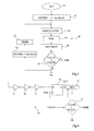
- the figure 2 is a block diagram illustrating an embodiment of a preparatory phase of a method of detecting a reset attack of the type described above, applied to the first aspect.
- the objective is to determine a pattern which will then be stored in a non-volatile memory of the circuit to be transferred, at each initialization, into the volatile memory dedicated to the protection.
- a pattern is stored in a volatile memory (block 31, PROT RAM) dedicated to the protection or control memory. It is important that this memory is different from the memory to be protected (12, figure 1 ) or, at the very least, that the power supply of this memory can be cut off / activated at will (at each verification). Indeed, it must be able to be switched off and on again independently of the volatile memory to be protected which would otherwise lose its content with each verification.
- the preparatory phase is carried out either after the manufacture of the memory, or during an initialization process of the protection method implemented, for example on command, during operation of the integrated circuit.
- switch-off time is preferably configurable (block 34, TIME) and can take different values. Typically, this delay is between a few microseconds and a few seconds.
- the re-ignition circuit causes the reading of the contents of the memory (block 34, READ ProtRAM). This reading is carried out of course without a reset of the memory.
- the object of the reading is to determine the number of memory cells that have changed state under the effect of extinction / ignition. It is not a question of finding the motive "pattern" stored in the memory, but of determining the effect on the memory of the extinction / ignition.
- the number of state changes is stored (block 35, HISTOGRAM) and the process is repeated several times (block 36, REPEAT). The object of this repetition is to determine the histogram of the number of state changes statistically at the start of the memory.
- the steps are preferably repeated for several patterns (arrow 37), for several times (arrow 38) and several temperatures (arrow 39 and block 40 - TEMP). Alternatively, they are also repeated for several supply voltages.
- step 31 is stored in the memory ProtRAM. To execute the process according to several interruption periods, it returns to the extinction stage 32. To execute the process with several temperatures, it returns before step 31 to try again with different patterns.
- An objective of this learning phase is, for a given reason, to determine in which statistical interval is the number of changes of states following an extinction / ignition for mainly different temperatures and preferably different periods of power off and different supply voltages.
- the Hamming distance between the pattern is determined. reference and current pattern by combining their respective states by a No-Exclusive (XNOR) comparison.
- one or more patterns and one or more extinction times are extracted from this learning phase which are the most representative in terms of information on the temperature of the circuit.
- the figure 3 is a histogram illustrating the implementation of the learning phase described in relation to the figure 2 .
- This figure illustrates an example of number of cells having changed states for a given pattern and temperature.
- a Gaussian centered on 48%, ranging between 40 and 60%.
- This histogram makes it possible, for example, to set an interval in number of state changes which, if it is not respected during an operational phase verification, means that the risk of being in the presence of an attack is high.
- the protection RAM memory is configured for, at each reset, to be loaded with the pattern.
- the figure 4 represents, in the form of blocks, an embodiment of an integrated circuit 1, equipped with "cold-boot” type detection detection circuits.
- NVM non-volatile memory 52
- the detection circuit 5 comprises a protection circuit 54 (PROT IC), for example according to the first aspect a volatile memory (31, figure 2 ) dedicated to protection or according to the second aspect which will be described in relation to figures 7 and following, a ring oscillator, and a control circuit 56 (CTRL).
- the circuit 56 provides an OK / NOK detection result, for example, to the processing unit 16, in order to take countermeasures (for example, a blocking of the circuit 1) in the event of a detected attack.
- control circuit 56 controls the transfer of the pattern stored in the memory 52 to the memory 54 at each reset of the circuit.
- memories 52 and 54 have been illustrated as communicating only with the circuit 56. Alternatively, they can be connected to the buses 14 and, for the memory 52, also serve other functions.
- the figure 5 represents, in simplified manner and in block form, an embodiment of a method for detecting a cold-boot type attack implementing the first aspect.
- the pattern stored in the memory 52 is transferred (block 62, PATTERN -> Prot RAM) to the protection memory 54.
- the circuit 36 causes, preferably periodically (loop illustrated by the block 63, TIMER), a verification procedure 60.
- This procedure begins with an extinction (block 64, SWITCH DOWN), followed after a power off time (block 65, TIME), a re-ignition (block 66, SWITCH UP) of the control memory 54 (here the memory 31 , figure 2 ).
- the circuit 56 (or the unit 16 according to whether the embodiment is hardware or software) then causes the reading of the control memory to count the number of cells having changed state and checks whether this number is included in the interval associated with the pattern (block 67, COUNT C RANGE?).
- the range RANGE of allowed values is, for example, stored with the pattern in non-volatile memory and is then read at each check.
- the characterization phase has made it possible to determine a pattern that does not need to be recharged, that is to say that, within the permitted temperature range, the extinction / ignition of the reference memory leads to a COUNT account remaining in the allowed range without reloading the pattern.
- step 62 ' is avoided.
- the periodicity of the test is chosen short enough so that the number of possible attacks per interrupt between two tests is not sufficient for an attacker to discover the sensitive information.
- the pattern comprises between 8 and 64 bits.
- the figure 6 represents the electrical diagram of an embodiment according to the second aspect.
- this oscillator comprises three inverters 71, 72 and 73 connected in series, the output of the last inverter 73 being looped back to the input of the first 71 and being connected to a data input D of a flip-flop D 74.
- the input The clock of the flip-flop 74 receives a clock signal CLK and its output, for example direct Q, provides a detection signal OUT.
- the sampling carried out by the flip-flop D provides a succession of states at the rhythm of the clock CLK.
- the clock input of the flip-flop is controlled by a ring oscillator distinct from the oscillator 54 '.
- the signal OUT is interpreted to determine its variation with respect to a reference signal within a permitted operating temperature range.
- the signal OUT is sent at the input of a shift register 75 (REG) at the rhythm of the clock CLK, storing a result from the previous outputs of the ring oscillator.
- REG shift register 75
- COUNT C RANGE COUNT C RANGE
- the response of the ring oscillator varies as a function of the temperature which influences the thermal noise of the transistors, which conditions the input state changes D of the flip-flop 74.
- the statistical response ie the state of the output bit of flip-flop 74 or, more precisely, the number of "0" or "1" in the register 75
- the interval RANGE to compare the response of the circuit 54 ' is, as in the embodiment based on a dedicated memory, stored in non-volatile memory 32.
- FIGS. 7A, 7B, 7C, 8A, 8B, 8C illustrate the operation of the circuit according to the second aspect, respectively in "normal" operation ( Figures 7A to 7C ) and in the presence of an attack by cooling the circuit ( Figures 8A to 8C ).
- the Figures 7A and 8A illustrate examples of the appearance of the input signal D of the flip-flop 74.
- the Figures 7B and 8B illustrate corresponding examples of clock signal CLK.
- the Figures 7C and 8C illustrate corresponding examples of the output signal Q of the flip-flop 74, thus of the contents of the register 75.
- the oscillations In the normal operating range of the circuit, the oscillations have some form (arbitrary). In the presence of a cooling attack, the oscillation pattern of the ring oscillator is disturbed. On the clock side, assuming a stable clock, cooling has the effect of changing the frequency but not the duty cycle. Thus, the output signal of the flip-flop 75 has a different pace than in the absence of attack.
- circuit of another nature is integrated to play the role of the circuit 54 '. What is important is to have an integrated circuit whose statistical response of an output signal is different when it is subjected to repeated extinguishing / burning with cooling compared to this response during stable operation.
Landscapes
- Engineering & Computer Science (AREA)
- Computer Security & Cryptography (AREA)
- Computer Hardware Design (AREA)
- Theoretical Computer Science (AREA)
- Software Systems (AREA)
- Physics & Mathematics (AREA)
- General Engineering & Computer Science (AREA)
- General Physics & Mathematics (AREA)
- Storage Device Security (AREA)
Abstract
L'invention concerne un procédé de détection d'une attaque par refroidissement d'un circuit intégré (1) comportant les étapes suivantes : transférer (62), dans une première mémoire volatile du circuit intégré, un motif stocké dans une mémoire non volatile du circuit ; provoquer périodiquement une extinction (64) et un allumage (66) de la première mémoire volatile ; vérifier (67) que le nombre de bits ayant changé d'état est compris dans une plage de valeurs.The invention relates to a method for detecting an attack by cooling an integrated circuit (1) comprising the steps of: transferring (62), in a first volatile memory of the integrated circuit, a pattern stored in a non-volatile memory of circuit; periodically quenching (64) and igniting (66) the first volatile memory; verifying (67) that the number of bits having changed state is within a range of values.
Description
La présente description concerne, de façon générale, les circuits électroniques, et plus particulièrement les circuits contenant des éléments stockant des données de façon volatile. La présente description s'applique plus particulièrement aux systèmes électroniques intégrés (System On Chip).The present description relates generally to electronic circuits, and more particularly to circuits containing elements storing data in a volatile manner. The present description applies more particularly to integrated electronic systems (System On Chip).
Dès qu'un système électronique manipule des données numériques, ces données sont stockées au moins temporairement dans des éléments des circuits électroniques. Il s'agit typiquement d'éléments de mémorisation volatile de type mémoire vive (RAM), ou de registres ou de bascules stockant des données binaires lorsqu'elles sont traitées par le circuit électronique.As soon as an electronic system manipulates digital data, this data is stored at least temporarily in elements of the electronic circuits. These are typically volatile memory storage elements (RAM), or registers or latches storing binary data when processed by the electronic circuit.
En principe, ces données disparaissent lorsque le circuit intégré n'est plus alimenté. En fait, elles ne disparaissent pas réellement, mais l'état qu'elles représentent n'est plus fiable lors de la remise en route du circuit.In principle, these data disappear when the integrated circuit is no longer powered. In fact, they do not really disappear, but the state they represent is no longer reliable when restarting the circuit.
Dans des circuits manipulant des quantités numériques considérées comme secrètes, c'est-à-dire dont l'accès doit être réservé à des utilisateurs ou à des circuits autorisés, on doit veiller à ce que les données manipulées par un circuit intégré de façon volatile ne soient plus accessibles dans les éléments de mémorisation pour des applications autres que les applications autorisées. Des zones de la mémoire vive affectées à ces applications sont donc généralement réservées. Cette réservation est cependant dynamique, c'est-à-dire qu'elle disparait lors de l'extinction ou d'une réinitialisation du circuit. Il faut donc s'assurer que les données contenues dans des zones précédemment réservées ne soient plus accessibles, par exemple, après redémarrage du système électronique. En effet, même si l'extinction du circuit rend ces données non fiables, elles sont susceptibles de contenir, même partiellement, des informations secrètes. On prévoit donc habituellement une première étape de réinitialisation des éléments de mémoire volatile à l'allumage d'un circuit électronique qui consiste à effacer la mémoire à l'allumage. Une telle technique prend du temps.In circuits handling digital quantities considered to be secret, that is to say the access of which must be reserved for authorized users or circuits, it must be ensured that the data handled by an integrated circuit in a volatile manner no longer accessible in the elements storage for applications other than authorized applications. Areas of the RAM allocated to these applications are therefore generally reserved. This reservation is however dynamic, that is to say it disappears when the circuit is shut down or reset. It must therefore be ensured that the data contained in previously reserved zones are no longer accessible, for example after restarting the electronic system. Indeed, even if the extinction of the circuit makes these data unreliable, they are likely to contain, even partially, secret information. It is therefore usually provided a first step of resetting the volatile memory elements to the ignition of an electronic circuit which consists of erasing the memory on ignition. Such a technique takes time.
Le document
Le document
Un mode de réalisation vise à pallier tout ou partie des inconvénients des systèmes électroniques manipulant de façon volatile des données considérées comme secrètes ou à accès réservés à certaines applications.One embodiment aims to overcome all or part of the disadvantages of electronic systems that manipulate in a volatile manner data considered as secret or access reserved for certain applications.
Un autre mode de réalisation vise à proposer un procédé de protection de données numériques contenues dans des éléments de stockage volatile d'un circuit intégré.Another embodiment aims to provide a method for protecting digital data contained in volatile storage elements of an integrated circuit.
Selon un premier aspect, un mode de réalisation vise une solution particulièrement adaptée à la protection de données stockées dans des zones d'une mémoire volatile.According to a first aspect, an embodiment aims at a solution that is particularly suitable for protecting data stored in areas of a volatile memory.
Selon un autre aspect, un mode de réalisation vise une détection exploitant des circuits simples.According to another aspect, an embodiment aims at a detection exploiting simple circuits.
Ainsi, un mode de réalisation prévoit un procédé de détection d'une attaque par refroidissement d'un circuit intégré comportant les étapes suivantes :
- transférer, dans une première mémoire volatile du circuit intégré, un motif stocké dans une mémoire non volatile du circuit ;
- provoquer périodiquement une extinction et un allumage de la première mémoire volatile ; et
- vérifier que le nombre de bits ayant changé d'état est compris dans une plage de valeurs.
- transferring, into a first volatile memory of the integrated circuit, a pattern stored in a non-volatile memory of the circuit;
- periodically causing extinction and ignition of the first volatile memory; and
- check that the number of bits that have changed state is within a range of values.
Selon un mode de réalisation, le motif est rechargé dans la première mémoire volatile avant chaque extinction.According to one embodiment, the pattern is reloaded in the first volatile memory before each extinction.
Selon un mode de réalisation, le motif est choisi pour que ledit nombre de bits changeant d'état varie en fonction de la température du circuit intégré.According to one embodiment, the pattern is chosen so that said number of bits changing state varies according to the temperature of the integrated circuit.
Selon un mode de réalisation, ladite plage de valeurs est déterminée par analyse statistique des états pris par les bits de la première mémoire volatile lors d'allumages successifs dans une phase d'apprentissage.According to one embodiment, said range of values is determined by statistical analysis of the states taken by the bits of the first volatile memory during successive ignitions in a learning phase.
Selon un mode de réalisation, des informations à protéger sont contenues dans une deuxième mémoire volatile, distincte de la première.According to one embodiment, information to be protected is contained in a second volatile memory, distinct from the first.
Un mode de réalisation prévoit un circuit intégré comportant :
- une première mémoire volatile ;
- une mémoire non volatile ; et
- des éléments adaptés à la mise en oeuvre du procédé ci-dessus.
- a first volatile memory;
- non-volatile memory; and
- elements adapted to the implementation of the method above.
Selon un mode de réalisation, le circuit comporte en outre une deuxième mémoire volatile, distincte de la première et contenant des informations à protéger contre des attaques par allumages successifs et refroidissement du circuit intégré.According to one embodiment, the circuit further comprises a second volatile memory, distinct from the first and containing information to be protected against attacks by successive ignitions and cooling of the integrated circuit.
Selon un mode de réalisation, le circuit comporte en outre un circuit de commande provoquant, à chaque initialisation du circuit intégré, un transfert dudit motif de la mémoire non volatile vers la première mémoire volatile.According to one embodiment, the circuit further comprises a control circuit causing each initialization of the integrated circuit, a transfer of said pattern from the non-volatile memory to the first volatile memory.
Ces caractéristiques et avantages, ainsi que d'autres, seront exposés en détail dans la description suivante de modes de réalisation particuliers faite à titre non limitatif en relation avec les figures jointes parmi lesquelles :
- la
figure 1 est un schéma bloc d'un exemple de circuit électronique du type auquel s'appliquent les modes de réalisation qui vont être décrits ; - la
figure 2 est une représentation schématique d'un mode de réalisation d'une première phase d'un procédé de protection du contenu d'une mémoire vive selon le premier aspect ; - la
figure 3 illustre un exemple d'histogramme obtenu par la mise en oeuvre du procédé de lafigure 2 ; - la
figure 4 est un schéma-bloc d'un mode de réalisation d'un circuit intégré équipé d'un circuit de détection d'une attaque par refroidissement et allumage ; - la
figure 5 est une représentation schématique d'un mode de réalisation d'une deuxième phase du procédé de protection de lafigure 2 ; - la
figure 6 représente, de façon schématique et sous forme de blocs, un mode de réalisation d'un élément d'un circuit de détection selon le deuxième aspect ; et - les
figures 7A à 7C et 8A à 8C illustrent le fonctionnement du circuit de détection de lafigure 6 .
- the
figure 1 is a block diagram of an exemplary electronic circuit of the type to which the embodiments to be described apply; - the
figure 2 is a schematic representation of an embodiment of a first phase of a method for protecting the contents of a random access memory according to the first aspect; - the
figure 3 illustrates an example of a histogram obtained by implementing the method offigure 2 ; - the
figure 4 is a block diagram of an embodiment of an integrated circuit equipped with a detection circuit of an attack by cooling and ignition; - the
figure 5 is a schematic representation of an embodiment of a second phase of the method of protecting thefigure 2 ; - the
figure 6 schematically and in the form of blocks, an embodiment of an element of a detection circuit according to the second aspect; and - the
FIGS. 7A to 7C and 8A to 8C illustrate the operation of the detection circuit of thefigure 6 .
De mêmes éléments ont été désignés par de mêmes références aux différentes figures. Par souci de clarté, seuls les étapes et éléments utiles à la compréhension des modes de réalisation qui vont être décrits et ont été représentés seront détaillés. En particulier, la constitution d'une mémoire volatile n'a pas été détaillée, les modes de réalisation décrits étant compatibles avec les structures et caractéristiques usuelles de tels mémoires et éléments de stockage volatile. De plus, les circuits et systèmes électroniques incluant des éléments de mémorisation volatile dont le contenu doit être protégé n'ont pas non plus été détaillés, les modes de réalisation décrits étant là encore compatibles avec les circuits et systèmes usuels.The same elements have been designated with the same references in the various figures. For the sake of clarity, only the steps and elements useful for understanding the embodiments that will be described and shown will be detailed. In particular, the constitution of a volatile memory has not been detailed, the described embodiments being compatible with the structures and characteristics usual such memories and volatile storage elements. In addition, electronic circuits and systems including volatile storage elements whose contents must be protected have also not been detailed, the embodiments described being again compatible with the usual circuits and systems.
La
La mémoire 12 stocke différentes données manipulées par les différents circuits, et notamment par l'unité de traitement 16. Dans des applications où le circuit électronique manipule des quantités secrètes, qu'il s'agisse de données ou d'algorithmes, une ou plusieurs zones de la mémoire 12 sont dédiées à ces applications dites sécurisées. Pour cela, lors de la mise en route du circuit ou lors d'une initialisation, l'unité de traitement 16 ou une unité dédiée à la mémoire (Memory Management Unit, par exemple) configure des droits d'accès à ces zones de la mémoire 12 et, par exemple, réserve l'accès de certaines zones à des programmes autorisés à manipuler les données secrètes.The
Un problème qui se pose est la vulnérabilité des données stockées dans la mémoire volatile à des attaques consistant à provoquer une réinitialisation du circuit. En effet, lors d'une extinction et allumage du circuit, une interruption du processus de configuration des zones protégées ou du processus de réinitialisation de la mémoire vive peut rendre accessibles les données secrètes exploitées avant cette réinitialisation.A problem that arises is the vulnerability of the data stored in the volatile memory to attacks consisting in causing a reset of the circuit. Indeed, during an extinction and lighting of the circuit, an interruption of the process of configuration of protected areas or the RAM reset process may make available the secret data exploited prior to this reset.
Un exemple d'attaque de ce type est connu sous la désignation "Cold Boot" car elles sont souvent accompagnées d'un refroidissement du circuit intégré de façon à ralentir le processus de réinitialisation.An example of such an attack is known as "Cold Boot" because they are often accompanied by a cooling of the integrated circuit so as to slow down the reset process.
Ces attaques s'effectuent généralement de façon répétée, c'est-à-dire que l'attaquant provoque des extinctions et allumages successifs et à bref délai (pour que la réinitialisation de la mémoire n'ait pas le temps de se produire) du circuit intégré.These attacks are generally repeated, that is, the attacker causes successive extinctions and ignitions and at short notice (so that the reset memory does not have time to occur) of the integrated circuit.
L'inventeur s'est aperçu que, pour un même contenu de cellule dans une mémoire volatile, le devenir de ce contenu suite à une extinction et rallumage prenait, de façon statistique, majoritairement les mêmes valeurs. En d'autres termes, à partir d'un motif stocké dans une zone de la mémoire, un motif qui lui est lié, ou une proportion d'états 0 et d'états 1, se retrouve dans le contenu de cette mémoire à la suite de chaque réinitialisation. Il est alors possible de déterminer le motif ou la proportion d'états 0 et d'états 1 que prendra la mémoire suite au stockage du premier motif et des réinitialisations successives. Par motif, on entend un ensemble d'états binaires contenu dans la zone mémoire concernée.The inventor realized that, for the same cell content in a volatile memory, the fate of this content following an extinction and re-ignition took, statistically, mainly the same values. In other words, from a pattern stored in an area of the memory, a pattern related to it, or a proportion of
Selon un premier aspect, on prévoit de dédier, à la détection d'attaques de type cold boot, une mémoire volatile séparée de la mémoire stockant les données sensibles, de préférence de taille inférieure à la taille de la mémoire volatile utilisée par le circuit.According to a first aspect, provision is made to dedicate, to the detection of cold boot attacks, a volatile memory separated from the memory storing the sensitive data, preferably smaller than the size of the volatile memory used by the circuit.
Selon un deuxième aspect, on prévoit d'utiliser un oscillateur en anneau pour détecter une attaque de type cold boot. L'inventeur s'est en effet aperçu que la reproductibilité des états de sortie successifs d'une bascule échantillonnant une sortie d'un tel oscillateur est similaire à celle d'un motif dans une mémoire volatile. Une différence est cependant que le motif n'a pas à être choisi et est natif dans le cas d'un oscillateur en anneau.According to a second aspect, it is planned to use a ring oscillator to detect a cold boot attack. The inventor has indeed noticed that the reproducibility of the successive output states of a flip-flop sampling an output of such an oscillator is similar to that of a pattern in a volatile memory. One difference is that the pattern does not have to be chosen and is native in the case of a ring oscillator.
Dans les deux cas, on commence par déterminer, dans une phase préparatoire ou d'apprentissage, la valeur ou la proportion d'états que prend la mémoire dédiée ou la sortie de l'oscillateur suite à des réinitialisations soudaines. Cette détermination permet ensuite, dans une phase opérationnelle, de comparer la valeur ou la proportion d'états, par exemple périodiquement, pour détecter une éventuelle attaque.In both cases, one begins by determining, in a preparatory or learning phase, the value or the proportion of states that takes the dedicated memory or the output of the oscillator following sudden resets. This determination then makes it possible, in an operational phase, to compare the value or the proportion of states, for example periodically, to detect a possible attack.
La
L'objectif est de déterminer un motif qui sera ensuite stocké dans une mémoire non volatile du circuit pour être transféré, à chaque initialisation, dans la mémoire volatile dédiée à la protection.The objective is to determine a pattern which will then be stored in a non-volatile memory of the circuit to be transferred, at each initialization, into the volatile memory dedicated to the protection.
Ainsi, selon un mode de réalisation, dans une phase préparatoire ou d'apprentissage, on stocke un motif (pattern) dans une mémoire volatile (bloc 31, PROT RAM) dédiée à la protection ou mémoire témoin. Il est important que cette mémoire soit différente de la mémoire à protéger (12,
On provoque alors une extinction du circuit intégré (bloc 32, SWITCH DOWN), puis à bref délai un rallumage de ce circuit (bloc 33, SWITCH UP). Le délai entre l'extinction et l'allumage (durée de mise hors tension) est de préférence configurable (bloc 34, TIME) et peut prendre différentes valeurs. Typiquement, ce délai est compris entre quelques microsecondes et quelques secondes.It then causes an extinction of the integrated circuit (block 32, SWITCH DOWN), then promptly re-ignition of this circuit (block 33, SWITCH UP). The time between switch-off and switch-on (switch-off time) is preferably configurable (block 34, TIME) and can take different values. Typically, this delay is between a few microseconds and a few seconds.
Une fois le rallumage du circuit effectué, on provoque la lecture du contenu de la mémoire (bloc 34, READ ProtRAM). Cette lecture s'effectue bien entendu sans que l'on ait procédé à une réinitialisation de la mémoire. L'objet de la lecture est de déterminer le nombre de cellules mémoire qui ont changé d'état sous l'effet de l'extinction/allumage. Il ne s'agit pas de retrouver le motif "pattern" stocké dans la mémoire, mais de déterminer l'effet sur la mémoire de l'extinction/allumage. Le nombre de changement d'états est stocké (bloc 35, HISTOGRAM) et le processus est répété plusieurs fois (bloc 36, REPEAT). Cette répétition a pour objet de déterminer l'histogramme du nombre de changement d'états de façon statistique à l'allumage de la mémoire.Once the re-ignition circuit is performed, it causes the reading of the contents of the memory (
Les étapes sont de préférence répétées pour plusieurs motifs (flèche 37), pour plusieurs durées (flèche 38) et plusieurs températures (flèche 39 et bloc 40 - TEMP). En variante, elles sont également répétées pour plusieurs tensions d'alimentation.The steps are preferably repeated for several patterns (arrow 37), for several times (arrow 38) and several temperatures (
Pour exécuter le processus selon plusieurs motifs, on revient à l'étape 31 de stockage dans la mémoire ProtRAM. Pour exécuter le processus selon plusieurs durées d'interruption, on revient à l'étape d'extinction 32. Pour exécuter le processus avec plusieurs températures, on revient avant l'étape 31 pour réessayer avec différents motifs.To execute the process in several patterns,
Un objectif de cette phase d'apprentissage est, pour un motif donné, de déterminer dans quel intervalle statistique se situe le nombre de changements d'états suite à une extinction/allumage pour principalement différentes températures et préférentiellement différentes durées de mise hors tension et différentes tensions d'alimentation. Selon un mode de réalisation, on détermine la distance de Hamming entre le motif de référence et le motif courant en combinant leurs états respectifs par une comparaison de type Non OU-Exclusif (XNOR).An objective of this learning phase is, for a given reason, to determine in which statistical interval is the number of changes of states following an extinction / ignition for mainly different temperatures and preferably different periods of power off and different supply voltages. According to one embodiment, the Hamming distance between the pattern is determined. reference and current pattern by combining their respective states by a No-Exclusive (XNOR) comparison.
De préférence, on extrait de cette phase d'apprentissage un ou plusieurs motifs et une ou plusieurs durées d'extinction qui sont les plus représentatifs en termes de renseignement sur la température du circuit. En d'autres termes, on cherche un motif et une durée de mise hors tension pour lesquels la variation du nombre de changement d'états en fonction de la température du circuit est la plus significative. Ainsi, en phase opérationnelle, une extinction et un allumage de la mémoire témoin contenant ce motif permet d'évaluer la température du circuit et, par voie de conséquence, la probabilité d'être en présence d'une attaque.Preferably, one or more patterns and one or more extinction times are extracted from this learning phase which are the most representative in terms of information on the temperature of the circuit. In other words, we look for a pattern and a duration of power off for which the variation of the number of state changes as a function of the temperature of the circuit is the most significant. Thus, in operational phase, an extinction and ignition of the control memory containing this pattern makes it possible to evaluate the temperature of the circuit and, consequently, the probability of being in the presence of an attack.
La
Une fois le motif choisi, celui-ci est stocké dans une zone de mémoire non volatile du circuit 1. La mémoire RAM de protection est configurée pour, à chaque réinitialisation, être chargée avec le motif.Once the pattern chosen, it is stored in a nonvolatile memory area of the
La
On retrouve une unité de traitement 16, une mémoire volatile 12 à protéger et une ou plusieurs fonctions 18. Par ailleurs, le circuit 5 comporte une mémoire non volatile 52 (NVM). Cette mémoire n'est pas nécessairement dédiée à la protection mais peut être une mémoire servant aux autres fonctions du circuit. Elle peut par conséquent, contrairement à ce qui est représenté, être reliée aux bus 14.There is a
Le circuit 5 de détection comporte un circuit de protection 54 (PROT IC), par exemple selon le premier aspect une mémoire volatile (31,
Pour la mise en oeuvre du premier aspect, le circuit de commande 56 contrôle le transfert du motif stocké dans la mémoire 52 vers la mémoire 54 à chaque réinitialisation du circuit.For the implementation of the first aspect, the
Dans la représentation de la
La
A chaque initialisation (bloc 61, INIT) ou réinitialisation du circuit 5, le motif stocké dans la mémoire 52 est transféré (bloc 62, PATTERN -> Prot RAM) vers la mémoire de protection 54.At each initialization (block 61, INIT) or reinitialization of the
Puis, le circuit 36 provoque, de préférence périodiquement (boucle illustrée par le bloc 63, TIMER), une procédure de vérification 60.Then, the
Cette procédure commence par une extinction (bloc 64, SWITCH DOWN), suivie après un temps de mise hors tension (bloc 65, TIME), d'un rallumage (bloc 66, SWITCH UP) de la mémoire témoin 54 (ici la mémoire 31,
Si le nombre COUNT est hors de la plage (sortie N du bloc 67), cela signifie une forte probabilité d'être en présence d'une attaque, c'est-à-dire que le circuit a été refroidi depuis la dernière vérification, et le circuit 56 renvoi un état NOK.If the number COUNT is outside the range (output N of block 67), this means a high probability of being in the presence of an attack, that is to say that the circuit has been cooled since the last verification, and the
Selon une variante de réalisation, la phase de caractérisation a permis de déterminer un motif qui ne nécessite pas d'être rechargé, c'est-à-dire que, dans la plage de températures autorisées, l'extinction/allumage de la mémoire témoin conduit à un compte COUNT restant dans la plage autorisée sans rechargement du motif. Dans ce cas, on évite l'étape 62'.According to an alternative embodiment, the characterization phase has made it possible to determine a pattern that does not need to be recharged, that is to say that, within the permitted temperature range, the extinction / ignition of the reference memory leads to a COUNT account remaining in the allowed range without reloading the pattern. In this case, step 62 'is avoided.
La périodicité de réalisation du test est choisie suffisamment courte pour que le nombre d'attaques possibles par interruption entre deux tests ne soit pas suffisant à un attaquant pour découvrir les informations sensibles.The periodicity of the test is chosen short enough so that the number of possible attacks per interrupt between two tests is not sufficient for an attacker to discover the sensitive information.
Selon la finesse souhaitée dans la détection, on peut conserver plusieurs motifs pour différentes températures en mémoire non volatile et leurs réponses respectives. On peut alors sélectionner le motif à stocker en fonction de la température de fonctionnement du circuit (qu'il faut alors équiper d'un capteur de température) et mettre à jour le motif, dans la mémoire RAM de protection, en fonction de la température de fonctionnement. Bien entendu, cela s'effectue au prix d'un espace plus important dans la mémoire non volatile. A titre d'exemple particulier de réalisation, le motif comprend entre 8 et 64 bits.Depending on the desired fineness in the detection, one can keep several patterns for different temperatures in nonvolatile memory and their respective responses. We can then select the pattern to store according to the operating temperature of the circuit (which must be equipped with a temperature sensor) and update the pattern in the RAM protection, depending on the temperature Operating. Of course, this is done at the cost of a larger space in the non-volatile memory. As of a particular embodiment, the pattern comprises between 8 and 64 bits.
La
On prévoit d'intégrer, dans le circuit 5, un ou plusieurs oscillateurs en anneau. Dans l'exemple de la
Le signal OUT est interprété pour déterminer sa variation par rapport à un signal de référence dans une plage de températures de fonctionnement autorisées.The signal OUT is interpreted to determine its variation with respect to a reference signal within a permitted operating temperature range.
Par exemple le signal OUT est envoyé en entrée d'un registre à décalage 75 (REG) au rythme de l'horloge CLK, stockant un résultat issu des précédentes sorties de l'oscillateur en anneau. A chaque besoin de vérification (à chaque test de détection d'une attaque), on vérifie (bloc 77, COUNT C RANGE ?) si le nombre d'états "1" (ou le nombre d'états "0") dans le registre 75 est compris dans une plage autorisée RANGE.For example, the signal OUT is sent at the input of a shift register 75 (REG) at the rhythm of the clock CLK, storing a result from the previous outputs of the ring oscillator. At each verification requirement (at each attack detection test), one checks (block 77, COUNT C RANGE?) If the number of states "1" (or the number of states "0") in the
En effet, la réponse de l'oscillateur en anneau varie en fonction de la température qui influence le bruit thermique des transistors, ce qui conditionne les changements d'états en entrée D de la bascule 74.Indeed, the response of the ring oscillator varies as a function of the temperature which influences the thermal noise of the transistors, which conditions the input state changes D of the flip-
Comme pour le cas d'une mémoire volatile témoin décrit précédemment, on détermine, dans une phase d'apprentissage, la réponse statistique (c'est-à-dire l'état du bit de sortie de la bascule 74 ou, plus précisément, le nombre de "0" ou de "1" dans le registre 75) à différentes températures, afin de déterminer la sortie majoritaire prise à l'allumage. L'intervalle RANGE auquel comparer la réponse du circuit 54' est, comme dans le mode de réalisation à base d'une mémoire dédiée, stocké en mémoire non volatile 32.As in the case of a volatile memory control described above, in a learning phase, the statistical response (ie the state of the output bit of flip-
Par rapport au mode de réalisation de la
Les
Dans la plage de fonctionnement normal du circuit, les oscillations ont une certaine forme (arbitraire). En présence d'une attaque par refroidissement, l'allure des oscillations de l'oscillateur en anneau est perturbée. Côté signal d'horloge, en supposant une horloge stable, le refroidissement a pour effet de modifier la fréquence mais pas le rapport cyclique. Ainsi, le signal en sortie de la bascule 75 a une autre allure qu'en l'absence d'attaque.In the normal operating range of the circuit, the oscillations have some form (arbitrary). In the presence of a cooling attack, the oscillation pattern of the ring oscillator is disturbed. On the clock side, assuming a stable clock, cooling has the effect of changing the frequency but not the duty cycle. Thus, the output signal of the flip-
En variante, un circuit d'une autre nature est intégré pour jouer le rôle du circuit 54'. Ce qui importe, c'est de disposer d'un circuit intégré dont la réponse statistique d'un signal de sortie est différente lorsqu'il est soumis à des extinctions/allumages répétés avec refroidissement par rapport à cette réponse lors d'un fonctionnement stable.Alternatively, a circuit of another nature is integrated to play the role of the circuit 54 '. What is important is to have an integrated circuit whose statistical response of an output signal is different when it is subjected to repeated extinguishing / burning with cooling compared to this response during stable operation.
Des modes de réalisation particuliers ont été décrits. Diverses variantes et modifications apparaîtront à l'homme de l'art. En particulier, la mise en oeuvre pratique des modes de réalisation décrits est à la portée de l'homme du métier à partir des indications fonctionnelles données ci-dessus.Particular embodiments have been described. Various variations and modifications will be apparent to those skilled in the art. In particular, the practical implementation of the described embodiments is within the abilities of those skilled in the art from the functional indications given above.
Claims (6)
Applications Claiming Priority (1)
| Application Number | Priority Date | Filing Date | Title |
|---|---|---|---|
| FR1455257A FR3022057B1 (en) | 2014-06-10 | 2014-06-10 | PROTECTION OF DATA STORED IN A VOLATILE MEMORY |
Publications (2)
| Publication Number | Publication Date |
|---|---|
| EP2955661A1 true EP2955661A1 (en) | 2015-12-16 |
| EP2955661B1 EP2955661B1 (en) | 2016-06-15 |
Family
ID=51905223
Family Applications (1)
| Application Number | Title | Priority Date | Filing Date |
|---|---|---|---|
| EP15159615.2A Active EP2955661B1 (en) | 2014-06-10 | 2015-03-18 | Protection of data stored in a volatile memory |
Country Status (2)
| Country | Link |
|---|---|
| EP (1) | EP2955661B1 (en) |
| FR (1) | FR3022057B1 (en) |
Citations (2)
| Publication number | Priority date | Publication date | Assignee | Title |
|---|---|---|---|---|
| WO2011018414A2 (en) | 2009-08-14 | 2011-02-17 | Intrinsic Id B.V. | Physically unclonable function with tamper prevention and anti-aging system |
| FR2974648A1 (en) | 2011-04-29 | 2012-11-02 | St Microelectronics Rousset | Method for protecting RAM against attacks by injections of faults in integrated circuit, involves filling blank areas or unused areas of RAM with pattern, and monitoring entire RAM for possible modification of state of bit |
-
2014
- 2014-06-10 FR FR1455257A patent/FR3022057B1/en not_active Expired - Fee Related
-
2015
- 2015-03-18 EP EP15159615.2A patent/EP2955661B1/en active Active
Patent Citations (2)
| Publication number | Priority date | Publication date | Assignee | Title |
|---|---|---|---|---|
| WO2011018414A2 (en) | 2009-08-14 | 2011-02-17 | Intrinsic Id B.V. | Physically unclonable function with tamper prevention and anti-aging system |
| FR2974648A1 (en) | 2011-04-29 | 2012-11-02 | St Microelectronics Rousset | Method for protecting RAM against attacks by injections of faults in integrated circuit, involves filling blank areas or unused areas of RAM with pattern, and monitoring entire RAM for possible modification of state of bit |
Also Published As
| Publication number | Publication date |
|---|---|
| FR3022057B1 (en) | 2016-05-27 |
| FR3022057A1 (en) | 2015-12-11 |
| EP2955661B1 (en) | 2016-06-15 |
Similar Documents
| Publication | Publication Date | Title |
|---|---|---|
| EP2280364B1 (en) | Faults injection detector in an integrated circuit | |
| FR2704341A1 (en) | Device for protecting the keys of a smart card. | |
| FR2989504A1 (en) | REGISTER PROTECTED FROM FAULT INJECTION ATTACKS | |
| EP1220101B1 (en) | Method and device for protecting against unauthorised use of integrated circuits | |
| EP1832974A1 (en) | Electromagnetic Analysis Protection of a calculation in an electronic circuit | |
| EP1742407B1 (en) | Protection of digital data contained within an integrated circuit with a JTAG interface | |
| EP2955661B1 (en) | Protection of data stored in a volatile memory | |
| FR2923923A1 (en) | CHECKING DATA IN MEMORY | |
| WO2017103497A1 (en) | Method for writing in a non-volatile memory of an electronic entity, and related electronic entity | |
| EP1633074A1 (en) | Integrated circuit with coded securing signal, securing method, device and coded securing signal via a corresponding dynamic key. | |
| FR3022056A1 (en) | PROTECTION OF DATA STORED IN AN INTEGRATED CIRCUIT | |
| FR2808360A1 (en) | METHOD OF AGAINST MEASUREMENT IN A MICROCIRCUIT USING THE METHOD AND CHIP CARD COMPRISING SAID MICROCIRCUIT | |
| EP1168621A1 (en) | Integrated circuit with protection device | |
| EP4145704B1 (en) | Secure starting of a processing unit | |
| EP2195793A1 (en) | Method for generating masks in a communicating object and corresponding communicating object | |
| FR2974648A1 (en) | Method for protecting RAM against attacks by injections of faults in integrated circuit, involves filling blank areas or unused areas of RAM with pattern, and monitoring entire RAM for possible modification of state of bit | |
| WO2015033069A1 (en) | Method of setting up safety means in an electronic device with memory, and device for implementing said method | |
| FR2963455A1 (en) | PROTECTING SECRET KEYS | |
| FR3011656A1 (en) | METHOD AND DEVICE FOR REALIZING FUNCTION BY A MICROCIRCUIT | |
| EP2852921B1 (en) | Method and smart card for the transmission of information | |
| FR3075430A1 (en) | DATA PROCESSING METHOD AND ASSOCIATED ELECTRONIC DEVICE | |
| EP1949292A1 (en) | Method for securely handling data during the running of cryptographic algorithms on embedded systems | |
| FR3110005A1 (en) | Secure boot controller for an embedded system, embedded system and associated secure boot method | |
| EP1818846A1 (en) | Verification of the integrity of programs or of sequencing in a state machine | |
| EP4068134A1 (en) | Secure debugging |
Legal Events
| Date | Code | Title | Description |
|---|---|---|---|
| PUAI | Public reference made under article 153(3) epc to a published international application that has entered the european phase |
Free format text: ORIGINAL CODE: 0009012 |
|
| 17P | Request for examination filed |
Effective date: 20150318 |
|
| AK | Designated contracting states |
Kind code of ref document: A1 Designated state(s): AL AT BE BG CH CY CZ DE DK EE ES FI FR GB GR HR HU IE IS IT LI LT LU LV MC MK MT NL NO PL PT RO RS SE SI SK SM TR |
|
| AX | Request for extension of the european patent |
Extension state: BA ME |
|
| REG | Reference to a national code |
Ref country code: DE Ref legal event code: R079 Ref document number: 602015000073 Country of ref document: DE Free format text: PREVIOUS MAIN CLASS: G06F0021790000 Ipc: G06F0021750000 |
|
| GRAJ | Information related to disapproval of communication of intention to grant by the applicant or resumption of examination proceedings by the epo deleted |
Free format text: ORIGINAL CODE: EPIDOSDIGR1 |
|
| GRAP | Despatch of communication of intention to grant a patent |
Free format text: ORIGINAL CODE: EPIDOSNIGR1 |
|
| RIC1 | Information provided on ipc code assigned before grant |
Ipc: G06F 21/79 20130101ALI20160317BHEP Ipc: G06F 21/75 20130101AFI20160317BHEP |
|
| INTG | Intention to grant announced |
Effective date: 20160405 |
|
| GRAS | Grant fee paid |
Free format text: ORIGINAL CODE: EPIDOSNIGR3 |
|
| GRAA | (expected) grant |
Free format text: ORIGINAL CODE: 0009210 |
|
| AK | Designated contracting states |
Kind code of ref document: B1 Designated state(s): AL AT BE BG CH CY CZ DE DK EE ES FI FR GB GR HR HU IE IS IT LI LT LU LV MC MK MT NL NO PL PT RO RS SE SI SK SM TR |
|
| REG | Reference to a national code |
Ref country code: CH Ref legal event code: EP Ref country code: GB Ref legal event code: FG4D Free format text: NOT ENGLISH |
|
| REG | Reference to a national code |
Ref country code: IE Ref legal event code: FG4D Free format text: LANGUAGE OF EP DOCUMENT: FRENCH |
|
| REG | Reference to a national code |
Ref country code: AT Ref legal event code: REF Ref document number: 806825 Country of ref document: AT Kind code of ref document: T Effective date: 20160715 |
|
| REG | Reference to a national code |
Ref country code: DE Ref legal event code: R096 Ref document number: 602015000073 Country of ref document: DE |
|
| REG | Reference to a national code |
Ref country code: LT Ref legal event code: MG4D |
|
| REG | Reference to a national code |
Ref country code: NL Ref legal event code: MP Effective date: 20160615 |
|
| PG25 | Lapsed in a contracting state [announced via postgrant information from national office to epo] |
Ref country code: NO Free format text: LAPSE BECAUSE OF FAILURE TO SUBMIT A TRANSLATION OF THE DESCRIPTION OR TO PAY THE FEE WITHIN THE PRESCRIBED TIME-LIMIT Effective date: 20160915 Ref country code: LT Free format text: LAPSE BECAUSE OF FAILURE TO SUBMIT A TRANSLATION OF THE DESCRIPTION OR TO PAY THE FEE WITHIN THE PRESCRIBED TIME-LIMIT Effective date: 20160615 Ref country code: FI Free format text: LAPSE BECAUSE OF FAILURE TO SUBMIT A TRANSLATION OF THE DESCRIPTION OR TO PAY THE FEE WITHIN THE PRESCRIBED TIME-LIMIT Effective date: 20160615 |
|
| REG | Reference to a national code |
Ref country code: AT Ref legal event code: MK05 Ref document number: 806825 Country of ref document: AT Kind code of ref document: T Effective date: 20160615 |
|
| PG25 | Lapsed in a contracting state [announced via postgrant information from national office to epo] |
Ref country code: HR Free format text: LAPSE BECAUSE OF FAILURE TO SUBMIT A TRANSLATION OF THE DESCRIPTION OR TO PAY THE FEE WITHIN THE PRESCRIBED TIME-LIMIT Effective date: 20160615 Ref country code: LV Free format text: LAPSE BECAUSE OF FAILURE TO SUBMIT A TRANSLATION OF THE DESCRIPTION OR TO PAY THE FEE WITHIN THE PRESCRIBED TIME-LIMIT Effective date: 20160615 Ref country code: GR Free format text: LAPSE BECAUSE OF FAILURE TO SUBMIT A TRANSLATION OF THE DESCRIPTION OR TO PAY THE FEE WITHIN THE PRESCRIBED TIME-LIMIT Effective date: 20160916 Ref country code: RS Free format text: LAPSE BECAUSE OF FAILURE TO SUBMIT A TRANSLATION OF THE DESCRIPTION OR TO PAY THE FEE WITHIN THE PRESCRIBED TIME-LIMIT Effective date: 20160615 Ref country code: SE Free format text: LAPSE BECAUSE OF FAILURE TO SUBMIT A TRANSLATION OF THE DESCRIPTION OR TO PAY THE FEE WITHIN THE PRESCRIBED TIME-LIMIT Effective date: 20160615 Ref country code: NL Free format text: LAPSE BECAUSE OF FAILURE TO SUBMIT A TRANSLATION OF THE DESCRIPTION OR TO PAY THE FEE WITHIN THE PRESCRIBED TIME-LIMIT Effective date: 20160615 |
|
| PG25 | Lapsed in a contracting state [announced via postgrant information from national office to epo] |
Ref country code: EE Free format text: LAPSE BECAUSE OF FAILURE TO SUBMIT A TRANSLATION OF THE DESCRIPTION OR TO PAY THE FEE WITHIN THE PRESCRIBED TIME-LIMIT Effective date: 20160615 Ref country code: IS Free format text: LAPSE BECAUSE OF FAILURE TO SUBMIT A TRANSLATION OF THE DESCRIPTION OR TO PAY THE FEE WITHIN THE PRESCRIBED TIME-LIMIT Effective date: 20161015 Ref country code: RO Free format text: LAPSE BECAUSE OF FAILURE TO SUBMIT A TRANSLATION OF THE DESCRIPTION OR TO PAY THE FEE WITHIN THE PRESCRIBED TIME-LIMIT Effective date: 20160615 Ref country code: SK Free format text: LAPSE BECAUSE OF FAILURE TO SUBMIT A TRANSLATION OF THE DESCRIPTION OR TO PAY THE FEE WITHIN THE PRESCRIBED TIME-LIMIT Effective date: 20160615 Ref country code: IT Free format text: LAPSE BECAUSE OF FAILURE TO SUBMIT A TRANSLATION OF THE DESCRIPTION OR TO PAY THE FEE WITHIN THE PRESCRIBED TIME-LIMIT Effective date: 20160615 Ref country code: CZ Free format text: LAPSE BECAUSE OF FAILURE TO SUBMIT A TRANSLATION OF THE DESCRIPTION OR TO PAY THE FEE WITHIN THE PRESCRIBED TIME-LIMIT Effective date: 20160615 |
|
| REG | Reference to a national code |
Ref country code: FR Ref legal event code: PLFP Year of fee payment: 3 |
|
| PG25 | Lapsed in a contracting state [announced via postgrant information from national office to epo] |
Ref country code: AT Free format text: LAPSE BECAUSE OF FAILURE TO SUBMIT A TRANSLATION OF THE DESCRIPTION OR TO PAY THE FEE WITHIN THE PRESCRIBED TIME-LIMIT Effective date: 20160615 Ref country code: PL Free format text: LAPSE BECAUSE OF FAILURE TO SUBMIT A TRANSLATION OF THE DESCRIPTION OR TO PAY THE FEE WITHIN THE PRESCRIBED TIME-LIMIT Effective date: 20160615 Ref country code: SM Free format text: LAPSE BECAUSE OF FAILURE TO SUBMIT A TRANSLATION OF THE DESCRIPTION OR TO PAY THE FEE WITHIN THE PRESCRIBED TIME-LIMIT Effective date: 20160615 Ref country code: PT Free format text: LAPSE BECAUSE OF FAILURE TO SUBMIT A TRANSLATION OF THE DESCRIPTION OR TO PAY THE FEE WITHIN THE PRESCRIBED TIME-LIMIT Effective date: 20161017 Ref country code: ES Free format text: LAPSE BECAUSE OF FAILURE TO SUBMIT A TRANSLATION OF THE DESCRIPTION OR TO PAY THE FEE WITHIN THE PRESCRIBED TIME-LIMIT Effective date: 20160615 |
|
| REG | Reference to a national code |
Ref country code: DE Ref legal event code: R097 Ref document number: 602015000073 Country of ref document: DE |
|
| PLBE | No opposition filed within time limit |
Free format text: ORIGINAL CODE: 0009261 |
|
| STAA | Information on the status of an ep patent application or granted ep patent |
Free format text: STATUS: NO OPPOSITION FILED WITHIN TIME LIMIT |
|
| 26N | No opposition filed |
Effective date: 20170316 |
|
| PG25 | Lapsed in a contracting state [announced via postgrant information from national office to epo] |
Ref country code: DK Free format text: LAPSE BECAUSE OF FAILURE TO SUBMIT A TRANSLATION OF THE DESCRIPTION OR TO PAY THE FEE WITHIN THE PRESCRIBED TIME-LIMIT Effective date: 20160615 |
|
| PG25 | Lapsed in a contracting state [announced via postgrant information from national office to epo] |
Ref country code: SI Free format text: LAPSE BECAUSE OF FAILURE TO SUBMIT A TRANSLATION OF THE DESCRIPTION OR TO PAY THE FEE WITHIN THE PRESCRIBED TIME-LIMIT Effective date: 20160615 |
|
| PG25 | Lapsed in a contracting state [announced via postgrant information from national office to epo] |
Ref country code: MC Free format text: LAPSE BECAUSE OF FAILURE TO SUBMIT A TRANSLATION OF THE DESCRIPTION OR TO PAY THE FEE WITHIN THE PRESCRIBED TIME-LIMIT Effective date: 20160615 |
|
| REG | Reference to a national code |
Ref country code: IE Ref legal event code: MM4A |
|
| PG25 | Lapsed in a contracting state [announced via postgrant information from national office to epo] |
Ref country code: LU Free format text: LAPSE BECAUSE OF NON-PAYMENT OF DUE FEES Effective date: 20170318 |
|
| REG | Reference to a national code |
Ref country code: FR Ref legal event code: PLFP Year of fee payment: 4 |
|
| PG25 | Lapsed in a contracting state [announced via postgrant information from national office to epo] |
Ref country code: IE Free format text: LAPSE BECAUSE OF NON-PAYMENT OF DUE FEES Effective date: 20170318 |
|
| REG | Reference to a national code |
Ref country code: BE Ref legal event code: MM Effective date: 20170331 |
|
| PG25 | Lapsed in a contracting state [announced via postgrant information from national office to epo] |
Ref country code: BE Free format text: LAPSE BECAUSE OF NON-PAYMENT OF DUE FEES Effective date: 20170331 |
|
| PG25 | Lapsed in a contracting state [announced via postgrant information from national office to epo] |
Ref country code: MT Free format text: LAPSE BECAUSE OF FAILURE TO SUBMIT A TRANSLATION OF THE DESCRIPTION OR TO PAY THE FEE WITHIN THE PRESCRIBED TIME-LIMIT Effective date: 20160615 |
|
| PG25 | Lapsed in a contracting state [announced via postgrant information from national office to epo] |
Ref country code: AL Free format text: LAPSE BECAUSE OF FAILURE TO SUBMIT A TRANSLATION OF THE DESCRIPTION OR TO PAY THE FEE WITHIN THE PRESCRIBED TIME-LIMIT Effective date: 20160615 |
|
| REG | Reference to a national code |
Ref country code: CH Ref legal event code: PL |
|
| PG25 | Lapsed in a contracting state [announced via postgrant information from national office to epo] |
Ref country code: CH Free format text: LAPSE BECAUSE OF NON-PAYMENT OF DUE FEES Effective date: 20180331 Ref country code: LI Free format text: LAPSE BECAUSE OF NON-PAYMENT OF DUE FEES Effective date: 20180331 |
|
| PG25 | Lapsed in a contracting state [announced via postgrant information from national office to epo] |
Ref country code: HU Free format text: LAPSE BECAUSE OF FAILURE TO SUBMIT A TRANSLATION OF THE DESCRIPTION OR TO PAY THE FEE WITHIN THE PRESCRIBED TIME-LIMIT; INVALID AB INITIO Effective date: 20150318 |
|
| PG25 | Lapsed in a contracting state [announced via postgrant information from national office to epo] |
Ref country code: BG Free format text: LAPSE BECAUSE OF FAILURE TO SUBMIT A TRANSLATION OF THE DESCRIPTION OR TO PAY THE FEE WITHIN THE PRESCRIBED TIME-LIMIT Effective date: 20160615 |
|
| PG25 | Lapsed in a contracting state [announced via postgrant information from national office to epo] |
Ref country code: CY Free format text: LAPSE BECAUSE OF FAILURE TO SUBMIT A TRANSLATION OF THE DESCRIPTION OR TO PAY THE FEE WITHIN THE PRESCRIBED TIME-LIMIT Effective date: 20160615 |
|
| GBPC | Gb: european patent ceased through non-payment of renewal fee |
Effective date: 20190318 |
|
| PG25 | Lapsed in a contracting state [announced via postgrant information from national office to epo] |
Ref country code: MK Free format text: LAPSE BECAUSE OF FAILURE TO SUBMIT A TRANSLATION OF THE DESCRIPTION OR TO PAY THE FEE WITHIN THE PRESCRIBED TIME-LIMIT Effective date: 20160615 |
|
| PG25 | Lapsed in a contracting state [announced via postgrant information from national office to epo] |
Ref country code: GB Free format text: LAPSE BECAUSE OF NON-PAYMENT OF DUE FEES Effective date: 20190318 |
|
| PG25 | Lapsed in a contracting state [announced via postgrant information from national office to epo] |
Ref country code: TR Free format text: LAPSE BECAUSE OF FAILURE TO SUBMIT A TRANSLATION OF THE DESCRIPTION OR TO PAY THE FEE WITHIN THE PRESCRIBED TIME-LIMIT Effective date: 20160615 |
|
| REG | Reference to a national code |
Ref country code: DE Ref legal event code: R081 Ref document number: 602015000073 Country of ref document: DE Owner name: STMICROELECTRONICS INTERNATIONAL N.V., CH Free format text: FORMER OWNER: STMICROELECTRONICS (ROUSSET) SAS, ROUSSET, FR |
|
| PGFP | Annual fee paid to national office [announced via postgrant information from national office to epo] |
Ref country code: FR Payment date: 20230222 Year of fee payment: 9 |
|
| PGFP | Annual fee paid to national office [announced via postgrant information from national office to epo] |
Ref country code: DE Payment date: 20240220 Year of fee payment: 10 |