EP2953236A1 - Power transmitter, wireless power transfer system, and wireless power transfer method - Google Patents
Power transmitter, wireless power transfer system, and wireless power transfer method Download PDFInfo
- Publication number
- EP2953236A1 EP2953236A1 EP13873594.9A EP13873594A EP2953236A1 EP 2953236 A1 EP2953236 A1 EP 2953236A1 EP 13873594 A EP13873594 A EP 13873594A EP 2953236 A1 EP2953236 A1 EP 2953236A1
- Authority
- EP
- European Patent Office
- Prior art keywords
- power
- power supply
- supply coil
- power source
- coil
- Prior art date
- Legal status (The legal status is an assumption and is not a legal conclusion. Google has not performed a legal analysis and makes no representation as to the accuracy of the status listed.)
- Granted
Links
Images


Classifications
-
- H—ELECTRICITY
- H01—ELECTRIC ELEMENTS
- H01F—MAGNETS; INDUCTANCES; TRANSFORMERS; SELECTION OF MATERIALS FOR THEIR MAGNETIC PROPERTIES
- H01F38/00—Adaptations of transformers or inductances for specific applications or functions
- H01F38/14—Inductive couplings
-
- H—ELECTRICITY
- H02—GENERATION; CONVERSION OR DISTRIBUTION OF ELECTRIC POWER
- H02J—ELECTRIC POWER NETWORKS; CIRCUIT ARRANGEMENTS OR SYSTEMS FOR SUPPLYING OR DISTRIBUTING ELECTRIC POWER; SYSTEMS FOR STORING ELECTRIC ENERGY
- H02J50/00—Circuit arrangements or systems for wireless supply or distribution of electric power
- H02J50/05—Circuit arrangements or systems for wireless supply or distribution of electric power using capacitive coupling
-
- H—ELECTRICITY
- H02—GENERATION; CONVERSION OR DISTRIBUTION OF ELECTRIC POWER
- H02J—ELECTRIC POWER NETWORKS; CIRCUIT ARRANGEMENTS OR SYSTEMS FOR SUPPLYING OR DISTRIBUTING ELECTRIC POWER; SYSTEMS FOR STORING ELECTRIC ENERGY
- H02J50/00—Circuit arrangements or systems for wireless supply or distribution of electric power
- H02J50/10—Circuit arrangements or systems for wireless supply or distribution of electric power using inductive coupling
- H02J50/12—Circuit arrangements or systems for wireless supply or distribution of electric power using inductive coupling of the resonant type
-
- H—ELECTRICITY
- H02—GENERATION; CONVERSION OR DISTRIBUTION OF ELECTRIC POWER
- H02J—ELECTRIC POWER NETWORKS; CIRCUIT ARRANGEMENTS OR SYSTEMS FOR SUPPLYING OR DISTRIBUTING ELECTRIC POWER; SYSTEMS FOR STORING ELECTRIC ENERGY
- H02J50/00—Circuit arrangements or systems for wireless supply or distribution of electric power
- H02J50/40—Circuit arrangements or systems for wireless supply or distribution of electric power using two or more transmitting or receiving devices
-
- H—ELECTRICITY
- H02—GENERATION; CONVERSION OR DISTRIBUTION OF ELECTRIC POWER
- H02J—ELECTRIC POWER NETWORKS; CIRCUIT ARRANGEMENTS OR SYSTEMS FOR SUPPLYING OR DISTRIBUTING ELECTRIC POWER; SYSTEMS FOR STORING ELECTRIC ENERGY
- H02J50/00—Circuit arrangements or systems for wireless supply or distribution of electric power
- H02J50/90—Circuit arrangements or systems for wireless supply or distribution of electric power involving detection or optimisation of position, e.g. alignment
Definitions
- Embodiments discussed herein relate to a power source, a wireless power transfer system and a wireless power transfer method.
- one power supply coil may be a load of another power supply coil, so that the power transfer may not performed in an optimum state.
- the embodiments may be applied to a power source including at least two power supply coils, wherein an output of each power supply coils is independently controlled and is mutually influenced each other.
- the embodiments may be also applied to a wireless power transfer system including at least two power sources, wherein an output power of each of the power sources is independently controlled and is mutually influenced each other.
- a power source including a first power supply coil and a second power supply coil which are mutually affecting, including a first power supply driving the first power supply coil; a second power supply driving the second power supply coil; and a power transfer control unit.
- the power transfer control unit controls one of a phase difference and an intensity ratio between an output signal of the first power supply coil and an output signal of the second power supply coil in accordance with impedance information of the first power supply and the second power supply.
- the power source, the wireless power transfer system and the wireless power transfer method disclosed have an advantageous effect in that power transfer may be performed in an optimum state.
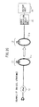
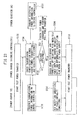
- FIG. 1 is a block diagram schematically depicting one example of a wireless power transfer system.
- reference sign 1 denotes a primary side (a power source side: a power source), and reference sign 2 denotes a secondary side (a power receiver side: a power receiver).
- power source 1 includes a wireless power transfer unit 11, a high frequency power supply unit 12, a power transfer control unit 13, and a communication circuit unit (a first communication circuit unit) 14.
- power receiver 2 includes a wireless power reception unit 21, a power reception circuit unit 22, a power reception control unit 23, and a communication circuit unit (a second communication circuit unit) 24.
- the wireless power transfer unit 11 includes a first coil (a power supply coil) 11b and a second coil (a power source resonance coil) 11a
- the wireless power reception unit 21 includes a third coil (a power receiver resonance coil) 21a and a fourth coil (a power extraction coil) 21b.
- the power source 1 and the power receiver 2 perform energy (electric power) transmission from the power source 1 to the power receiver 2 by magnetic field resonance (electric field resonance) between the power source resonance coil 11a and the power receiver resonance coil 21a.
- Power transfer from the power source resonance coil 11a to the c may be performed not only by magnetic field resonance but also electric field resonance or the like. However, the following description will be given mainly by way of example of magnetic field resonance.
- the power source 1 and the power receiver 2 communicate with each other (near field communication) by the communication circuit unit 14 and the communication circuit unit 24.
- a distance of power transfer (a power transfer range PR) by the power source resonance coil 11a of power source 1 and the power receiver resonance coil 21a of power receiver 2 is set to be shorter than a distance of communication (a communication range CR) by the communication circuit unit 14 of power source 1 and the communication circuit unit 24 of power receiver 2 (PR ⁇ CR).
- power transfer by the power source resonance coil 11a and the power receiver resonance coil 21a is performed by a system (an out-band communication) independent from communication by the communication circuit units 14 and 24.
- power transfer by the resonance coils 11a and 21a uses, for example, a frequency band of 6.78 MHz
- communication by the communication circuit units 14 and 24 uses, for example, a frequency band of 2.4 GHz.
- the communication by the communication circuit units 14 and 24 may use, for example, a DSSS wireless LAN system based on IEEE 802.11b or Bluetooth (registered trademark).
- the above described wireless power transfer system performs power transfer using magnetic field resonance or electric field resonance by the power source resonance coil 11a of the power source 1 and the power receiver resonance coil 21a of the power receiver 2, for example, in a near field at a distance of about a wavelength of a frequency used. Accordingly, the range of power transfer (a power transfer area) PR varies with the frequency used for power transfer.
- the high frequency power supply unit 12 supplies power to the power supply coil (the first coil) 11b, and the power supply coil 11b supplies power to the power source resonance coil 11a arranged very close to the power supply coil 11b by using electromagnetic induction.
- the power source resonance coil 11a transfers power to the power receiver resonance coil 21a (the power receiver 2) at a resonance frequency that causes magnetic field resonance between the resonance coils 11a and 21a.
- the power receiver resonance coil 21a supplies power to the power extraction coil (the fourth coil) 21b arranged very close to the power receiver resonance coil 21a, by using electromagnetic induction.
- the power extraction coil 21b is connected to the power reception circuit unit 22 to extract a predetermined amount of power.
- the power extracted from the power reception circuit unit 22 is used, for example, for charging a battery in the battery unit (load) 25, as a power supply output to the circuits of power receiver 2, or the like.
- the high frequency power supply unit 12 of power source 1 is controlled by the power transfer control unit 13, and the power reception circuit unit 22 of power receiver 2 is controlled by the power reception control unit 23. Then, the power transfer control unit 13 and the power reception control unit 23 are connected via the communication circuit units 14 and 24, and adapted to perform various controls so that power transfer from power source 1 to power receiver 2 may be performed in an optimum state.
- FIG. 2A to FIG. 2C are diagrams for illustrating modified examples of a transmission coil in the wireless power transfer system of FIG. 1 .
- FIG. 2A and FIG. 2B depict exemplary three-coil structures
- FIG. 2C depicts an exemplary two-coil structure.
- the wireless power transfer unit 11 includes the first coil 11b and the second coil 11a
- the wireless power reception unit 21 includes the third coil 21a and the fourth coil.
- the wireless power reception unit 21 is set as a single coil (a power receiver resonance coil: an LC resonator) 21a
- the wireless power transfer unit 11 is set as a single coil (a power source resonance coil: an LC resonator) 11a.
- the wireless power reception unit 21 is set as a single power receiver resonance coil 21a and the wireless power transfer unit 11 is set as a single power source resonance coil 11a.
- FIG. 2A to FIG. 2C are merely examples and, obviously, various modifications may be made.
- FIG. 3A to FIG. 3D are circuit diagrams depicting examples of an independent resonance coil (the power receiver resonance coil 21a), and FIG. 4A to FIG. 4D are circuit diagrams depicting examples of a resonance coil (the power receiver resonance coil 21a) connected to a load or a power supply.
- FIG. 3A to FIG. 3D correspond to the power receiver resonance coil 21a of FIG. 1 and FIG. 2B
- FIG. 4A to FIG. 4D correspond to the power receiver resonance coil 21a of FIG. 2A and FIG. 2C .
- the power receiver resonance coil 21a includes a coil (L) 211, a capacitor (C) 212, and a switch 213 connected in series, in which the switch 213 is ordinarily in an off-state.
- the power receiver resonance coil 21a includes the coil (L) 211 and the capacitor (C) 212 connected in series, and the switch 213 connected in parallel to the capacitor 212, in which the switch 213 is ordinarily in an on-state.
- the power receiver resonance coil 21a of FIG. 3B and FIG. 4B includes the switch 213 and the resistance (R) 214 connected in series and arranged in parallel to the capacitor 212, in which the switch 213 is ordinarily in the on-state.
- FIG. 3D and FIG. 4D depict the power receiver resonance coil 21a of FIG. 3B and FIG. 4B , in which the switch 213 and another capacitor (C') 215 connected in series are arranged in parallel to the capacitor 212, and the switch 213 is ordinarily in the on-state.
- the switch 213 is set to "off” or “on” so that the power receiver resonance coil 21a does not operate ordinarily.
- the reason for this is, for example, to prevent heat generation or the like caused by power transfer to a power receiver 2 not in use (on power receiver) or to a power receiver 2 out of order.
- the power source resonance coil 11a of power source 1 may also be set as in FIG. 3A to FIG. 3D and FIG. 4A to FIG. 4D .
- the power source resonance coil 11a of the power source 1 may be set so as to operate ordinarily and may be controlled to be turned on/off by an output of the high frequency power supply unit 12.
- the switch 213 is to be shortcircuited in FIG. 3A and FIG. 4A .
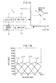
- FIG. 5A to FIG. 5C are diagrams for illustrating examples of controlling magnetic field by a plurality of power sources.
- reference signs 1A and 1B denote power sources
- reference sign 2 denotes a power receiver.
- an power source resonance coil 11aA for power transfer used for magnetic field resonance of the power source 1A and an power source resonance coil 11aB for power transfer used for magnetic field resonance of the power source 1B are arranged, for example, so as to be orthogonal to each other.
- the power receiver resonance coil 21a used for magnetic field resonance of the power receiver 2 is arranged at a different angle (an angle not parallel) at a position surrounded by the power source resonance coil 11aA and the power source resonance coil 11aB.
- the power source resonance coil (LC resonator) 11aA and 11aB for power transfer may also be provided in a single power source.
- a single power source 1 may include a plurality of wireless power transfer units 11.
- designating one of the plurality of power sources as a master and the other one or more power sources as slaves means that a CPU (Central Processing Unit) of the single master power source controls all of the resonance coils included in the master power source and the slave power sources.
- CPU Central Processing Unit
- FIG. 5B depicts a situation in which the power source resonance coils 11aA and 11aB output an in-phase magnetic field
- FIG. 5C depicts a situation in which the power source resonance coils 11aA and 11aB output a reverse phase magnetic field.
- a synthesized magnetic field becomes a 90° rotation relationship in each other, so that a power transfer is carried out to each power receiver 2 (power receiver resonance coil 21a) with suitably transmitting from the power source resonance coils 11aA and 11aB based on the postures of the power receiver 2.
- the wireless power transfer system of the present embodiment includes a plurality of power sources and at least one power receiver and adjusts outputs (strengths and phases) between the plurality of power sources according to positions (X, Y and Z) and postures ( ⁇ x, ⁇ y and ⁇ z) of the power receiver.
- FIG. 6 is a diagram for illustrating an example of a correspondence between a plurality of power sources and a plurality of power receivers according to a related art
- FIG. 7 is a diagram for illustrating a state of each power receiver in FIG. 6 . Note that FIG. 6 and FIG. 7 illustrate the case where two power sources 1A and 1B and five power receivers 2A to 2E are arranged.
- the single power source 1A of the plurality of power sources 1A and 1B is designated as a master (primary) and the other power source 1B is designated as a slave (secondary).
- the master the power source 1A determines processing such as optimization of the plurality of power sources and the power receiver.
- reference sign PRa denotes a power transfer area of the power source 1A (a master power transfer area); reference sign PRb denotes a power transfer area of the power source 1B (a slave power transfer area); reference sign CRa denotes a communication area of the power source 1A (a master communication area); and reference sign CRb denotes a communication area of the power source 1B (a slave communication area).
- statuses of the power receivers 2A to 2E are as follows. Specifically, as depicted in FIG. 7 , the power receiver 2A is outside the master communication area CRa (x), outside the slave communication area Crb, outside the master power transfer area PRa, and outside the slave power transfer area PRb, and simply waits for communication from the power sources.
- the power receiver 2B is located within the master communication area CRa (o), outside the slave communication area CRb, outside the master power transfer area PRa, and outside the slave power transfer area PRb.
- communicating with the master power source 1A allows for a confirmation that the power receiver 2B is outside the power areas (outside the master and slave power transfer areas).
- the power receiver 2C is within the master communication area CRa, within the slave communication area CRb, outside the master power transfer area PRa, and outside the slave power transfer area PRb.
- communicating with the master and slave power sources 1A and 1B allows for a confirmation that the power receiver 2C is outside the power areas.
- the power receiver 2D is within the master communication area CRa, within the slave communication area CRb, within the master power transfer area PRa, and outside the slave power transfer area PRb.
- communicating with the master and slave power sources 1A and 1B allows for a confirmation that the power receiver 2D is within the power area of the power source 1A (within the master power transfer area PRa).
- the power receiver 2E is within the master communication area CRa, within the slave communication area CRb, within the master power transfer area PRa, and within the slave power transfer area PRb.
- communicating with the master and slave power sources 1A and 1B allows for a confirmation that the power receiver 2E is within the power areas of the power sources 1A and 1B (within the power transfer areas PRa and PRb).
- a single power source is determined as a master.
- the master may be determined, for example, depending on a condition in which a largest number of power receivers are located within the communication area of the power source or within the power transfer area thereof, as described later.
- the master when there is an equal condition in which each one power receiver is located within the communication areas of the power sources, the master may be determined by adding an additional condition such as a communication strength between the power source and the power receiver, or an arbitrary one power source may be determined as a master using a random number table or the like.
- designating one of the plurality of power sources as a master allows the master power source to control optimization for the power sources including the other one or more slave power sources.
- FIG. 8A to FIG. 8C are diagrams for illustrating correspondence between the plurality of power sources and the plurality of power receivers, and illustrating how to determine a master and slaves in the plurality of power sources.
- a master power source and slave power sources are determined in the plurality of power sources when the power sources are located within communication ranges (communication areas) of each other, power transfer ranges (power transfer areas) of the power sources overlap each other, and the relevant power receiver detects the overlapping of the power transfer areas.
- FIG. 8A depicts a situation in which the communication area CRa of the power source 1A overlaps the communication area CRb of the power source 1B, whereas the power transfer area PRa of the power source 1A does not overlap the power transfer area PRb of the power source 1B.
- both the power sources 1A and 1B are designated as respective master power sources.
- FIG. 8B depicts a situation in which the communication area CRa and the power transfer area PRa of the power source 1A overlap the communication area CRb and the power transfer area PRb of the power source 1B and the power receiver 2 is included in both the power transfer areas PRa and PRb.
- the power sources 1A and 1B are located within the communication areas CRa and CRb of each other, the power transfer areas PRa and PRb overlap each other, and moreover, the power receiver 2 detects the overlapping of the power transfer areas PRa and PRb.
- one (1A) of the power sources 1A and 1B is designated as a master power source and the other one (1B) thereof is designated as a slave power source.
- the power source 1B may be designated as a master and the power source 1A may be designated as a slave, either one of the power sources 1A and 1B is designated as a master power source.
- FIG. 8C depicts a situation in which the power sources 1A and 1B are arranged in the same positional relationship as that in FIG. 8B described above, but the power receiver 2 is not present (not located within the communication areas CRa and CRb). In this situation, both the power sources 1A and 1B are designated as masters.
- any one of the power sources is designated as a master power source.
- Various methods may be considered to designate a single master power source from the plurality of power sources. One example of the methods will be described with reference to FIG. 9 .
- FIG. 9 is a diagram (4) for illustrating correspondence between the and a plurality of power sources and the plurality of power receivers, in which four power sources 1A to 1D are arranged in a line.
- a communication area CRa of the power source 1A includes the power source 1B but does not include the power sources 1C and 1D.
- a communication area CRd of the power source 1D includes the power source 1C but does not include the power sources 1A and 1B.
- a communication area CRb of the power source 1B includes the power sources 1A and 1C but does not include the power source 1D.
- a communication area CRc of the power source 1C includes the power sources 1B and 1D but does not include the power source 1A.
- the power source 1B is designated as a mater (a master power source) and the other power sources 1A, 1C and 1D are designated as slaves (slave power sources).
- the power source 1C may be designated as a master.
- designating the power source 1B as a master power source makes it difficult to directly communicate with the power source 1D.
- the power source 1B communicates with the power source 1D via the power source 1C to control optimization, and the like. Therefore, it is preferable to designate, as a master, a power source that may directly communicate with a largest number of power sources when designating a single master from a plurality of power sources.
- the four power sources 1A to 1D are arranged in a straight line.
- a plurality of power sources will be disposed in various positional relationships, for example, by being embedded in a wall or a ceiling of a room, being built in a desk or a table, or being mounted on a floor, a table, or the like.
- FIG. 10 is a diagram for illustrating a power transfer plan design in a singular power source. Specifically, FIG. 10 illustrates an equivalent circuit model including one power source 1 and one power receiver 2, for example, so as to explain the case of performing power transfer from the power source 1 to the power receiver 2, as depicted in above described FIG. 1 .
- references V S and R S correspond to a high-frequency power supply unit 12; L 1 and R 1 correspond to a power supply coil (first coil) 11b; and C 2 , L 2 and R 2 correspond to a power source resonance coil (second coil: LC resonator) 11a.
- references C 3 , L 3 and R 3 correspond to a power receiver resonance coil (third coil: LC resonator) 21a; L 4 and R 4 correspond to a power extraction coil (fourth coil) 21b; and R L corresponds to a load (battery unit) 25.
- the capacitance values C 2 and C 3 , and resistance values R L and R S are already known, and resistance values R 1 to R 4 , inductance values L 1 to L 4 , and mutual inductance values M 12 , M 13 , M 14 , M 23 , M 24 and M 34 may be calculated from electromagnetic field simulations.
- a transmission power P IN may be calculated from a formula [reception power P OUT ]/[power transmitting and receiving efficiency (P OUT /P IN )]. Therefore, a proper reception power P OUT may be applied to the load R L by inputting the calculated transmission power P IN into the power supply coil 11b.
- the power transmitting and receiving efficiency is also referred to as power transfer efficiency.
- FIG. 11 is a diagram for illustrating a power transfer plan design in a plurality of power sources. Specifically, FIG. 11 illustrates an equivalent circuit model including two power sources 1A and 1B, and one power receiver 2, for example, so as to explain the case of performing power transfer from the power sources 1A and 1B to the power receiver 2, as depicted in above described FIG. 5A .
- references V S1 and R S1 correspond to a high-frequency power supply unit 12A of the power source 1A; V S2 and R S2 correspond to a high frequency power supply unit 12B of the power source 1B. Further, L 11 and R 11 correspond to a power supply coil 11bA of the power source 1A; and L 12 and R 12 correspond to a power supply coil 11bB of the power source 1B.
- references C 21 , L 21 and R 21 correspond to a power source resonance coil 11aA of the power source 1A; and C 22 , L 22 and R 22 correspond to a power source resonance coil 11aB of the power source 1B.
- the power receiver 2 is similar to that depicted in FIG. 10 , and references C 3 , L 3 and R 3 correspond to the power receiver resonance coil 21a; L 4 and R 4 correspond to the power extraction coil 21b; and R L corresponds to the load 25.
- the capacitance values C 21 , C 22 and C 3 , and the resistance values R L , R S1 and R S3 are already known, and the resistance values R 11 , R 12 , R 21 , R 22 , R 3 and R 4 , and the inductance values L 11 , L 12 , L 21 , L 22 , L 3 and L 4 may be calculated from electromagnetic field simulations.
- mutual inductance values M 112 , M 122 , M 113 , M 114 , M 213 , M 214 , M 123 , M 124 , M 223 , M 224 , M 111 , M 111 ', M 222 , M 222 ' and M 34 may be also calculated from the electromagnetic field simulations.
- set values of V S1 and V S2 include a phase difference between V S1 and V S2 and an intensity ratio between V S1 and V S2 .
- R S1 included in the power source 1A is considered as a load which is the same as the power receiver from the power source 1B
- R S2 included in the power source 1B is considered as a load which is the same as the power receiver from the power source 1A. Therefore, the impedances R S1 and R S2 of the high frequency power supply units 12A and 12B affect the power transfer efficiency of the wireless power transfer system depicted in FIG. 11 .
- FIG. 12 FIG. 13A and FIG. 13B , as well as, FIG. 14 , FIG. 15A and FIG. 15B , where posture dependencies of power supply transmission efficiencies are varied in accordance with power supply impedances of a plurality of power sources in the wireless power transfer using the plurality of power sources.
- FIG. 12 is a diagram for illustrating an example of a wireless power transfer system with the plurality of power sources.
- references 11a1 and 11a2 denote power source 1 of the power source resonance coil (second coil: LC resonator), 15 denotes an oscillator, 16 denotes a phase control unit, 171 and 172 denote amplifiers, and 21a denotes a power receiver resonance coil (LC resonator: third coil) of the power receiver 2.
- FIG. 12 illustrates the case where the power source 1 includes two power source resonance coils 11a1 and 11a2 capable of controlling a phase and an intensity, performs power transfer to the power receiver 2 via the power receiver resonance coil 21a.
- a size of the power receiver resonance coil 21a of the power receiver 2 is assumed sufficiently smaller than that of the power source resonance coils 11a1 and 11a2.
- the power source resonance coil 11a1 corresponds to a first power supply coil
- the power source resonance coil 11a2 corresponds to a second power supply coil.
- an oscillation signal generated by the oscillator 15 is input to the amplifier 171, and to the amplifier 172 via the phase control unit 16.
- the phase control unit 16 adjusts a phase difference between output phases of the amplifiers 171 and 172, by controlling a phase of the signal input to the amplifier 172.
- the amplifiers 171 and 172 amplify and output the input oscillation signals, respectively, an output of the amplifier 171 is input to the power source resonance coil 11a1 (wireless power transfer unit 111), and an output of the amplifier 172 is input to the power source resonance coil 11a2 (wireless power transfer unit 112).
- phase difference between the amplifiers 171 and 172 is adjusted by controlling a phase of the oscillation signal performed by the phase control unit 16, and the intensity ratio between the amplifiers 171 and 172 is adjusted by controlling intensities of the amplification factors of the amplifiers 171 and 172.
- phase control performed by using the phase control unit 16, and the control of the amplification factors performed by using the amplifiers 171 and 172 may be carried out in accordance with the power transfer control unit 13 depicted in FIG. 1 .
- the amplifiers (high frequency power supply units) 171 and 172 in FIG. 12 include an AC impedance characteristics, and the impedance characteristics (impedances R S1 and R S2 depicted in FIG. 11 ) of the high frequency power supply units may affect the power transfer efficiency.
- FIG 12 although two power source resonance coils 11a1 and 11a2 of the power source 1 are arranged in orthogonal, the power source resonance coils 11a1 and 11a2 may be included in different power sources 1A and 1B as depicted in FIG. 5A .
- each of the power sources 1A and 1B includes an oscillator, and the phase difference between the output signals may be adjusted by exchanging the phase information via the respective communication units of the power sources 1A and 1B. Further, regarding the adjustments of the intensity ratios of the power sources 1A and 1B, similar features may be applied.
- the phase control (control of the phase difference) may be performed by using the communication between the power sources 1A and 1B.
- control of the phase difference and the intensity ratio of the output signals of two power sources 1A and 1B may be performed in accordance with a power transfer control unit 13 of a master power source 1A via communication circuit units 14A and 14B, which will be explained later in detail with reference to FIG. 16 .
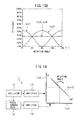
- FIG. 13A is a diagram for illustrating a posture dependency of a power transfer efficiency in the case of applying a constant voltage power supply in a wireless power transfer system depicted in FIG. 12 .
- FIG. 13B is a diagram for illustrating a posture dependency of a power transfer efficiency in the case of applying a constant current power supply in a wireless power transfer system depicted in FIG. 12 .
- the constant voltage power supply outputs a signal of 6.78 MHz to be used for performing power transfer, and an output impedance of the constant voltage power supply is matched to a range from several ⁇ to several tens of ⁇ (as one example, 50 ⁇ ).
- various kind of high frequency power supply units each including an output impedance of 50 ⁇ which may be applied to the present embodiments, have been proposed and widely used in the technical art of communications.
- the frequency to be used for power transfer is not limited to 6.78 MHz, further matching output impedance may be set to 75 ⁇ instead of 50 ⁇ , and the impedance of 75 ⁇ may be also applied to the present embodiments.
- the constant current power supply which outputs a signal of 6.78 MHz to be used for performing power transfer, may be a power supply including a high output impedance (high impedance power supply: Hi-Z ⁇ power supply).
- the output impedance of the constant current power supply is not limited, but may be preferably larger than 1M ⁇ .
- the constant current power supply may be referred to as 0 ⁇ -power supply, based on input characteristics thereof. An example of the constant current power supply will be explained later in detail with reference to FIG. 24 .
- a horizontal axis represents a rotation angle of the power receiver resonance coil 21a (posture of the power receiver 2)
- a vertical axis represents a power transfer efficiency.
- curved lines LL11 and LL21 indicate the case when the phase difference between the transmission outputs from the power source resonance coils 11aA and 11aB is at 0° (in-phase)
- curved lines LL12 and LL22 indicate the case when the phase difference between the transmission outputs from the power source resonance coils 11aA and 11aB is at 90°.
- curved lines LL13 and LL23 indicate the case when the phase difference between the transmission outputs from the power source resonance coils 11aA and 11aB is at 180° (reverse phase)
- curved lines LL14 and LL24 indicate the case when the phase difference between the transmission outputs from the power source resonance coils 11aA and 11aB is at -90°.
- phase difference of the power source resonance coils 11aA and 11aB is set to 0° (LL11)
- maximum power transfer efficiency about 43%) is obtained by determining the rotation angle of the power receiver resonance coil 21a (power receiver 2) to 0° and 180°.
- phase difference of the power source resonance coils 11aA and 11aB is set to 90° (LL12)
- the maximum power transfer efficiency may be obtained by determining the rotation angle of the power receiver 2 to 135°
- the phase difference of the power source resonance coils 11aA and 11aB is set to 180° (LL13)
- the maximum power transfer efficiency is obtained by determining the rotation angle of the power receiver 2 to 90°.
- the phase difference of the power source resonance coils 11aA and 11aB is set to -90° (270°: LL14), it will be seen that the maximum power transfer efficiency may be obtained by determining the rotation angle of the power receiver 2 to 45°.
- the maximum power transfer efficiency may be obtained by preferably determining the phase difference of the power source resonance coils 11aA and 11aB.
- the phase difference of the power source resonance coils 11aA and 11aB is set to 0° (LL21) and 180° (LL23)
- the above described curbed lines LL11 and LL13 are upwardly distorted about a center value of the efficiency without changing the local maximum and minimum values.
- the efficiency may be a constant value (about 27%) regardless of the rotation angle of the power receiver 2, that is, without being affected by the posture of the power receiver 2.
- FIG. 14 is a diagram for illustrating another example of a wireless power transfer system with the plurality of power sources. Note that, in FIG. 12 described above, the size of the power receiver resonance coil 21a of the power receiver 2 is sufficiently smaller than that of the power source resonance coils 11a1 and 11a2. However, in FIG. 14 , a size of the power receiver resonance coil 21a is set to the same degree of that of the power source resonance coils 11a1 and 11a2.
- binding properties between the power source (power source resonance coils 11a1 and 11a2) and the power receiver (power receiver resonance coil 21a) are different in the examples of FIG. 14 and FIG. 12 .
- FIG. 14 is a diagram for illustrating another example of a wireless power transfer system with the plurality of power sources. Note that, in FIG. 12 described above, the size of the power receiver resonance coil 21a of the power receiver 2 is sufficiently smaller than that of the power source resonance coils 11a1 and 11a2. However, in FIG. 14 , a size of the power receiver resonance coil 21a is set to the same degree of that of the power source resonance coils 11a1 and 11a2. Note that, other features and conditions are the same as in FIG. 12 and FIG. 14 , and thus explanations thereof will be omitted.
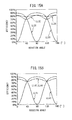
- FIG. 15A is a diagram for illustrating a posture dependency of a power transfer efficiency in the case of applying a constant voltage power supply in the wireless power transfer system depicted in FIG. 14 , which corresponds to above described FIG. 13A .
- FIG. 15B is a diagram for illustrating the posture dependency of a power transfer efficiency in the case of applying a constant current power supply in the wireless power transfer system depicted in FIG. 14 , which corresponds to above described FIG. 13B .
- a horizontal axis represents a rotation angle of the power receiver resonance coil 21a (posture of the power receiver 2)
- a vertical axis represents a power transfer efficiency.
- curved lines LL31 and LL41 indicate the case when the phase difference between the transmission outputs from the power source resonance coils 11aA and 11aB is at 0° (in-phase)
- curved lines LL32 and LL42 indicate the case when the phase difference between the transmission outputs from the power source resonance coils 11aA and 11aB is at 90°.
- curved lines LL33 and LL43 indicate the case when the phase difference between the transmission outputs from the power source resonance coils 11aA and 11aB is at 180°
- curved lines LL34 and LL34 indicate the case when the phase difference between the transmission outputs from the power source resonance coils 11aA and 11aB is at -90°.
- FIG. 15A and FIG. 15B By comparing FIG. 15A and FIG. 15B with above described FIG. 13A and FIG. 13B , in the case when a size of the power receiver resonance coil 21a is set to the same degree of that of the power source resonance coils 11a1 and 11a2, a power transfer efficiency may be increased. This is because when the power receiver resonance coil 21a is large, it is possible to receive a sufficient output power from the power source resonance coils 11a1 and 11a2.
- the local maximum value and the center value of the power transfer efficiency are upwardly distorted without changing the local minimum value of the power transfer efficiency.
- the maximum value of the power transfer efficiency is significantly increased from about 43% depicted in FIG. 13A to about 90% depicted in FIG. 15A .
- the local minimum values of the curved lines LL32 and LL34 approach about 70%, however, the local maximum values of the curved lines LL32 and LL34 are lower than the local maximum value of the curved lines LL31 and LL33 (but higher than 80%).
- the local maximum value and the center value of the power transfer efficiency are upwardly distorted without changing the local minimum value of the power transfer efficiency.
- the curbed lines LL41 and LL43 are substantially coincident with the curbed lines LL31 and LL33 depicted in DIG. 15A.
- the power transfer efficiency may be constant (about 75% to 84%) without being affected by the posture of the power receiver 2.
- power levels of respective power sources may be determined by selecting a combination of variable parameters for obtaining desired power transfer efficiency characteristics, so that, for example, power transfer by the maximum power transfer efficiency or a power transfer by a high robustness efficiency may be selectively realized.
- FIG. 16 is a block diagram for illustrating an example of a wireless power transfer system of the present embodiment, wherein two power sources 1A and 1B, and two power receivers 2A and 2B are included.
- the power sources 1A and 1B include the same configurations, and the power source 1A, 1B includes a wireless power transfer unit 11A, 11B, a high frequency power supply unit 12A, 12B, a power transfer control unit 13A, 13B, and a communication circuit unit 14A, 14B.
- the high frequency power supply unit 12A, 12B generates an electric power of a high frequency, for example, which corresponds to the high frequency power supply unit 12 depicted in FIG. 1 as described above, or corresponds to the amplifier 171, 172 including a specific power supply impedance depicted in FIG. 12 and FIG. 14 .
- the high frequency power supply unit 12A, 12B is a constant voltage power supply including an output impedance which is matched to 50 ⁇ or a Hi-Z ⁇ power supply (constant current power supply) including a high output impedance, and the like.
- the power transfer control unit 13A, 13B controls the wireless power transfer unit 11A, 11B, and may include, for example, an oscillator 15 and a phase control unit 16 as depicted in FIG. 12 and FIG. 14 .
- the communication circuit unit 14A, 14B enables to communicate among the power sources and the power receivers, which may be realized by using, for example, a DSSS type wireless LAN based on the IEEE 802.11b or a Bluetooth (registered trademark).
- the high frequency power supply unit 12A, 12B receives a power from an external power supply 10A, 10B, and the power transfer control unit 13A, 13B receives a signal from a detection unit SA, SB, respectively.
- the power sources 1A and 1B may be formed as two wireless power transfer units (11) provided in one power source 1.
- the wireless power transfer unit 11A, 11B corresponds to a coil in the case of applying magnetic field resonance, and converts a high frequency power output from the high frequency power supply unit 12A, 12B into magnetic field.
- the detection unit SA, SB detects a positional relationship of the power sources 1A and 1B or a positional relationship of the power receivers 2A and 2B. Note that, a method for detecting the positional relationship may be applied, for example, an imaging system by using a plurality of cameras.
- the positional relationship of the power sources 1A and 1B is fixed (power source resonance coils 11a1 and 11a2 are fixed as a particular L-shaped block), when the information is confirmed by the power transfer control units 13A and 13B and the power receivers 2A and 2B include detection function thereof, the detection units SA and SB may be omitted.
- the power receivers 2A and 2B include the same configurations, and the power receiver 2A, 2B includes a wireless power reception unit 21A, 21B, a rectifier (power receiving circuit) 22A, 22B, a power reception control unit 23A, 23B, a communication circuit unit 24A, 24B, and an apparatus body (battery unit) 25A, 25B.
- the power receiver 2A, 2B includes a wireless power reception unit 21A, 21B, a rectifier (power receiving circuit) 22A, 22B, a power reception control unit 23A, 23B, a communication circuit unit 24A, 24B, and an apparatus body (battery unit) 25A, 25B.
- the power reception control unit 23A, 23B controls the power receiver 2A, 2B, and the communication circuit unit 24A, 24B enables to communicate among the power sources and the power receivers, which may be realized by using, for example, a Bluetooth (registered trademark).
- the wireless power receiving unit 21A, 21B is equivalent to a coil for converting an electric power wirelessly transmitted to a current.
- the rectifier 22A, 22B converts an alternating current obtained by the wireless power receiving unit 21A, 21B to a direct current used for charging a battery or driving an apparatus body.
- the power sources 1A and 1B, and the power receivers 2A and 2B may communicate each other by using respective communication circuit units 14A, 14B and 24A, 24B.
- this master (power source) 1A may control the other power source 1B and power receivers 2A and 2B as slaves.
- wireless power transfer using magnetic field resonance between the wireless power transfer units 11A and 11B, and the wireless power reception units 21A or 21B, but, for example, electric field resonance, electromagnetic induction, and electric field induction may be also applied to the wireless power transfer system.
- FIG. 17 and FIG. 18 are flowcharts for illustrating examples of processes in the wireless power transfer system depicted in FIG. 16 . Specifically, FIG. 16 illustrates the process when the power receiver is absent, and FIG. 17 illustrates the process when the power receiver is present.
- FIG. 17 and FIG. 18 illustrate the case when the power source 1A is a master (entire controller) and the power source 1B is a slave.
- communication between the slave power source 1B and the master power source 1A is performed by the communication circuit units 14A and 14B, and communication between the power receivers 2A, 2B and the master power source 1A is performed by the communication circuit units 24A, 24B and 14A.
- the master power source 1A checks to detect other power sources (slave power source 1B) and confirms the other power source (slave power source 1B) by using communication.
- the communication may be performed by either wireless or wired.
- the slave power source 1B transmits a presence of the other power source to the master power source 1A, and when the master power source 1A may establish the communication with the other power source and confirm an ID of the other power source in step ST13, the master power source 1A may determine the presence of the other power source. Note that, when the master power source 1A does not detect the other power source, the power transfer is performed based on single power source, which is already explained with reference to FIG. 10 .
- the master power source 1A detects the other power source (slave power source 1B), in step ST14, for example, the master power source 1A checks a relative positional relationship regarding to the slave power source 1B using a detection unit SA. Note that, when the relative position of the master power source 1A and the slave power source 1B does not overlap a transfer range, for example, relative distances thereof are faraway, etc., the power transfer is performed based on a single power source, which is already explained with reference to FIG. 10 .
- step ST14 the master power source 1A checks a relative positional relationship regarding to the slave power source 1B by using, for example, a detection unit SA. In the case of detecting a possibility that the transfer ranges overlap the other power source (slave power source 1B), the processing proceeds to step ST15. Specifically, in step ST11, the slave power source 1B transmits power source information to the master power source 1A, and the master power source 1A confirms the position of the power transfer unit (wireless power transfer unit) 11B of the slave power source 1B.
- the slave power source 1B transmits power source information to the master power source 1A
- the master power source 1A confirms the position of the power transfer unit (wireless power transfer unit) 11B of the slave power source 1B.
- step ST12 the slave power source 1B transmits a power supply impedance to the master power source 1A, and the processing proceeds to step ST16, the master power source 1A checks the power supply impedance of the power source 1B.
- steps ST12 and ST16 it is determined whether the power supply of the slave power source 1B and the power supply of itself (master power source 1A) are constant voltage power supplies matched to, for example, 50 ⁇ or constant current power supplies of Hi-Z ⁇ .
- the information transmitted from the slave power source 1B to the master power source 1A is, for example, information (data) which will be explained later in detail with reference to FIG. 19 .
- step ST17 the master power source 1A searches a power supply target.
- This power supply target search operation is performed by using respective communication circuit units (14A, 14B, 24A, 24B), and he master power source 1A searches power receivers 2A and 2B.
- the slave power sources may be plural. Further, the search operation for searching power receivers (2A, 2B) performed by the master power source 1A may be carried out by wireless communications, and the search operation for searching power receivers may be continuously performed until a power receiver of the target receiver is found.
- step ST22 the master power source 1A (entire controller) searches target power receivers, that is, power receivers (2A, 2B).
- step ST28 the power receiver 2A transmits a presence to the master power source 1A.
- FIG. 18 illustrates the case of performing power transfer to the power receiver 2A, this power receiver 2A is also functioned as a slave to the master power source 1A.
- step ST28 the slave power receiver 2A transmits a presence of itself to the master power source 1A
- the processing proceeds to step ST22, the master power source 1A establishes a communication with the other power receiver, and the master power source 1A determines that the other power receiver may be searched when ID thereof is confirmed.
- the master power source 1A detects the other power receiver (slave power receiver 2A), in step ST23, the master power source 1A, for example, checks a relative positional relationship regarding to the slave power receiver 2A. Note that, when the transfer ranges do not overlap, for example, the relative positions of the master power source 1A and the slave power receiver 2A are far away, and the like, the master power source 1A determines that the other power receiver is not detected.
- step ST24 the master power source 1A checks a power reception unit (wireless power reception unit) 21A of the confirmed slave power receiver 2A. Specifically, in step ST29, the slave power receiver 2A transmits power receiver information to the master power source 1A.
- a power reception unit wireless power reception unit
- This power receiver information includes, for example, information such as a size of the power receiver resonance coil (21a) of the power receiver 2A, and the like.
- the information transmitted from the slave power receiver 2A to the master power source 1A is, for example, information (data) which will be explained later in detail with reference to FIG. 20
- the master power source 1A formulates an optimization plan based on all information.
- the all information to be used for the master power source 1A may include, for example, the power supply impedance information checked in step ST16 depicted in FIG. 17 , and the size information of the power receiver resonance coil (21a) of the power receiver 2A, checked in step ST24, and the like.
- step ST26 the master power source 1A transmits a phase difference and an intensity ratio (phase-intensity conditions) to the respective power sources (slave power source 1B).
- step ST20 the slave power source 1B receives the phase-intensity conditions from the master power source 1A, and the processing proceeds to step ST21, the slave power source 1B starts power transfer in accordance with the phase-intensity conditions.
- step ST27 the master power source 1A starts power transfer.
- the start of power transfer by the master power source 1A in step ST27 and the start of power transfer by the slave power source 1B in step ST21 may be synchronously performed by using, for example, the communication circuit units 14A and 14B.
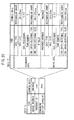
- FIG. 19 is a diagram for illustrating an example of the transmission information between the power sources, for example, an example of transmission information of transmitting information from the slave power source 1B to the master power source 1A.
- the transmission information transmitted from the slave power source 1B to the master power source 1A includes, for example, a product ID of DATA 1, or actual data of respective items as depicted in DATA 2.
- the master power source 1A may read out data from a memory table, which is previously provided in the master power source 1A, and the master power source 1A may recognize the respective items of DATA 2 which corresponds to DATA 2 based on the transmitted product ID as similar to the above.
- the master power source 1A connects to the Internet via a wired or wireless line, and downloads the latest data corresponding to the transmitted product ID from a predetermined external server or web site, so that the master power source 1A may recognize data of the respective items.
- the information transmitted from the slave power source 1B to the master power source 1A may include, for example, the information of the power source resonance coil 11aB and the power supply coil 11bB, and also the information relating to the power supply impedances as described above.
- the items depicted in FIG. 19 are only an example, and the items may be variously modified.
- FIG. 20 is a diagram for illustrating an example of the transmission information between the power source and the power receiver, for example, illustrates an example of information transmitted from the slave power receiver 2A to the master power source 1A.
- the transmission information transmitted from the slave power receiver 2A to the master power source 1A includes, for example, a product ID, a charge request and a remaining battery capacity as depicted in DATA 1.
- the master power source 1A may recognize the respective items as depicted in DATA 2 by using a memory table provided in the master power source 1A or a predetermined web site via the Internet.
- the slave power receiver 2A may transmit information in addition to the charge request and the remaining battery capacity to the master power source 1A, for example, information of respective actual items as depicted in DATA 2 instead of the product ID.
- the items depicted in FIG. 20 are only an example, and the items may be variously modified.
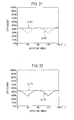
- FIG. 21 is a diagram for illustrating an optimization process of parameters in the case of applying a constant voltage power supply in the wireless power transfer system depicted in FIG. 12 , and illustrates simulation results by using the constant voltage power supply including an output impedance of 50 ⁇ .
- a curved line LL61 indicates change of a power transfer efficiency with respect to a rotation angle of the power receiver resonance coil 21a (power receiver 2) when an intensity ratio of output signals of the power source resonance coils 11a1 and 11a2 (amplifiers 171 and 172) is fixed and a phase difference is optimized.
- a curved line LL62 indicates change of a power transfer efficiency with respect to a rotation angle of the power receiver 2 when a phase difference of the output signals of the power source resonance coils 11a1 and 11a2 is fixed to 0° (in-phase) or 180° (reverse phase), and an intensity ratio is optimized.
- the maximum efficiency may not always obtained by variously adjusting the intensity ratio.
- the maximum power transfer efficiency may be always obtained by fixing the intensity ratio of the output signals and variously adjusting the phase difference of the output signals.
- the dominant parameter for optimizing to obtain the maximum power transfer efficiency is the phase difference of the output signals.
- FIG. 22 is a diagram for illustrating an optimization of the parameters in the case of applying a constant current power supply in a wireless power transfer system depicted in FIG. 12 , and illustrates simulation results by using the constant current power supply of including an output impedance of Hi-Z ⁇ .
- a curved line LL71 indicates change of a power transfer efficiency with respect to a rotation angle of the power receiver 2 when an intensity ratio of output signals is fixed and a phase difference is optimized.
- a curved line LL72 indicates change of a power transfer efficiency with respect to a rotation angle of the power receiver 2 when a phase difference of the output signals is fixed to in-phase or reverse phase, and an intensity ratio is optimized.
- the maximum efficiency may not always obtained, even if the phase difference of the output signals are variously adjusted.
- the maximum power transfer efficiency may be always obtained by fixing the phase difference of the output signals to in-phase or reverse phase and variously adjusting the intensity ratio of the output signals.
- the dominant parameter for optimizing to obtain the maximum power transfer efficiency is the intensity ratio of the output signals.
- setting conditions corresponding to the formulated optimization plan are transmitted to the phase control unit 16 and the amplifiers 171 and 172 of the power source 1, and then, power transfer based on the setting conditions may be started.
- FIG. 23 is a flowchart illustrating an example of the optimization processes of parameters depicted in FIG. 21 and FIG. 22 , and illustrates an example of performing a test power transfer.
- step ST30 when starting the test power transfer, the processing proceeds to step ST34, the power source 1A checks a transmission power and a reception power, and also checks a power transmitting and receiving efficiency (power transfer efficiency). Specifically, in step ST31, the slave power source 1B transmits a transmission power of itself to the entire controller (master power source 1A), and in step ST37, the slave power receiver 2A transmits a reception power of itself to the master power source 1A,
- step ST35 the master power source 1A determines whether or not the checked power transmitting and receiving efficiency is a desired efficiency.
- step ST34 it is determined that the checked power transmitting and receiving efficiency is the desired efficiency, the test power transfer is finished and a full power transfer is performed.
- step ST34 it is determined that the checked power transmitting and receiving efficiency is not the desired efficiency, the processing proceeds to step ST36, an optimization plan is reformulated by changing a dominant parameter corresponding to the power supply impedance as explained with reference to FIG. 21 and FIG. 22 .
- step ST36 in the case of applying a power supply of 50 ⁇ , the optimization plan may be reformulated by changing the phase difference of the power supply.
- the optimization plan in the case of applying a power supply of Hi-Z ⁇ , the optimization plan may be reformulated by changing the intensity ratio of the power supply. Therefore, the optimization plan may be reformulated in a short time by adjusting the dominant parameter in accordance with the power supply impedance.
- step ST36 the master power source 1A sets a phase and an intensity in accordance with the reformulated optimization plan, the processing proceeds to step ST33, and a test power transfer may be restarted.
- step ST33 the master power source 1A restarts the test power transfer, and then the processing returns to step ST34, the similar processes may be repeatedly performed.
- step ST32 the slave power source 1B receives the phase and intensity conditions which are determined in accordance with the reformulated optimization plan in step ST36, sets the received phase and intensity conditions, and the processing proceeds to step ST33, the test power transfer may be restarted.
- step ST33 After starting the test power transfer in step ST33, the processing returns to step ST34, and the slave power source 1B repeats the similar processes.
- the phase difference and the intensity ration are not independently changed, but the dominant parameter obtained from the power supply impedance information is changed, so that it may be possible to formulate an optimization plan in a short time.
- a first embodiment is a wireless power transfer method where power transfer efficiency is prioritized
- the second embodiment is a wireless power transfer method where a high-robust is prioritized.
- the first embodiment used to prioritize the power transfer efficiency will be explained.
- power transfer for portable electronic devices for example, power capacity of several Watts to several dozen Watts
- a transferring power is relatively large, and thus, a high efficiency may be required.
- the power transfer efficiency is decreased, an electric power may be consumed and a temperature of the power source may be increased, especially, this problem is serious when the transferring (transmitting) power becomes large.
- the various sensors are originally provided, and various types of information obtained by the various sensors may be transmitted from the portable electronic devices to the power source side (master power source).
- the master power source may be obtained relative positional relationship information of the power receiver.
- the phase difference is varied with fixing the intensity ratio of the power supply, so that the maximum efficiency may be obtained.
- a constant current power supply Hi-Z ⁇ power supply
- each of the sensors is required to constitute a small size and a low cost, and thus posture detect functions may not provide on all of the sensors as the portable electronics devices.
- those curved lines LL22 and LL24 are the case when the phase difference of power transmission outputs of the power source resonance coils 11aA and 11aB is at 90° and -90°, however, the phase difference is not limited to these values.
- phase difference when the phase difference may be shifted in a certain range from 90° and -90°, although affected by the rotation angle may become large, a high robust in the practical postures may be obtained.
- FIG. 24 is a block diagram for illustrating an example of a constant current power supply, and an example of a high-frequency power supply unit 12.
- the constant current power supply 12 includes an AC signal generation unit 121, an operational amplifier (op amp) 122, a current buffer 123, a reference resistor 124, a feedback resistor 125 and a capacitor 126, and an output terminal of the constant current power supply 12 is connected with a load.
- the load corresponds to a power supply coil (first coil) 11b.
- the AC signal generation unit 121 generates a reference AC voltage (for example, frequency is at 6.78 MHz, and magnitude of the AC voltage is constant), and the reference AC voltage is applied to a non-inverting input (positive input) of the operational amplifier 122. Note that, an inverting input (negative input) of the operational amplifier 122 is grounded via the reference resistor 124, and an output signal of the operational amplifier 122 is input to the current buffer 123.
- a reference AC voltage for example, frequency is at 6.78 MHz, and magnitude of the AC voltage is constant
- the constant current power supply (and the constant voltage power supply) to be applied to the present embodiment is not limited to those for outputting a signal of 6.78 MHz, but of course the frequency may be varied in accordance with the frequency to be used for power transfer.
- An output of the current buffer 123 is input to one end of a load (power supply coil) 11b via the capacitor 126, and grounded via the feedback resistor 125 and the reference resistor 124.
- the other end of the power supply coil 11b is grounded via the reference resistor 124.
- an output impedance thereof is at a high impedance (Hi-Z ⁇ ).
- the constant current power supply of FIG. 24 is merely one example, various constant current power supplies may be applied to the present embodiments.
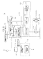
- FIG. 25 is a block diagram for illustrating an example of the power source (master power source 1A) in the wireless power transfer system depicted in FIG. 16 .
- the wireless power transfer unit 11A includes an LC resonator 11aA and a power supply coil 11bA.
- a high frequency power supply unit 12A includes an oscillator 127, an amplifier 128 and a matching device 129.
- the power transfer control unit 13A includes a power transfer control circuit 131 and a frequency lock circuit 132.
- the frequency lock circuit 132 receives a synchronization signal from the communication circuit unit 14A, and performs a synchronization process of the oscillator 127 by a predetermined interval (for example, several minutes to several ten minutes interval).
- the oscillator 127 generates a driving signal having a predetermined frequency (for example, 6.78 MHz), and the driving signal is output to the wireless power transfer unit 11A (power supply coil 11bA) via the amplifier 128 and the matching device 129.
- the power transfer control circuit 131 includes a CPU (processor) 134 connected by an internal bus 133, a memory 135 and an input-output circuit (I/O unit) 136.
- the memory 135 includes a rewritable non-volatile memory, e.g., a flash memory, and a DRAM (Dynamic Random Access Memory), and the like. Then, various processes (software programs) may be performed in the master power source 1A, the slave power source 1B and power receivers.
- the master power source 1A includes, for example, a detection unit SA for checking a relative positional relationship between the master power source 1A and the slave power source 1B.
- the output of the detection unit SA is, for example, input to the CPU 134 via the I/O unit 136, and is used to perform a software program (wireless power transfer program, or control program of the power source) stored in the memory 135.
- a portable recording medium for example, an SD (Secure Digital) memory card
- the program may be read out from a hard disk device 61 of a program (data) provider 60 via a communication line and the I/O unit 135, and stored in the memory 135.
- the communication line from the hard disk device 61 to the I/O unit 136 may be a wireless communication line by using the communication circuit unit 14.
- the recording medium (computer-readable recording medium) to which the portable wireless power transfer program is recorded may be a DVD (Digital Versatile Disk), a Blu-ray disc (Blu-ray Disc), and the like.
- power source and power receiver which has been described mainly as one or two, it may be a larger number, respectively. Further, in the description of respective embodiments, a power transfer is mainly explained by using magnetic field resonance. Nevertheless, the present embodiment may apply to the power transfer using electric field resonance, and to the power transfer using electromagnetic induction or electric field induction.
- the present embodiment may also apply to a wireless power transfer system including at least two power sources wherein outputs of the at least two power sources affect each other.
- each of the power sources may include at least one power transfer coil, and at least one of the phase or intensity of an output of the power transfer coil may be independently controlled.
- this embodiment is the same as the wireless power transfer system including at least two power sources, may also be applied to at least two power sources wireless power transfer system output mutually affect each other.
- Each of the power sources includes, for example, at least one transmitting coil enabling to independently control at least one of the phase or intensity.
Landscapes
- Engineering & Computer Science (AREA)
- Power Engineering (AREA)
- Computer Networks & Wireless Communication (AREA)
- Charge And Discharge Circuits For Batteries Or The Like (AREA)
- Near-Field Transmission Systems (AREA)
- Constitution Of High-Frequency Heating (AREA)
- Electric Ovens (AREA)
Abstract
Description
- Embodiments discussed herein relate to a power source, a wireless power transfer system and a wireless power transfer method.
- Recently, in order to perform power supply or perform charging, wireless power transfer techniques have been gaining attention. Research and development are being conducted regarding a wireless power transfer system wirelessly performing power transfer to various electronic apparatuses such as mobile terminals and notebook computers and household electrical appliances or to power infrastructure equipment.
- In order to use wireless power transfer, it is preferable to standardize so that no problem occurs in the use of a power source of a power source and a power receiver of a power receiver that are of different manufactures.
- Among conventional wireless power transfer techniques, a technique using electromagnetic induction and a technique using radio waves have generally been known.
- In recent years, expectations for power transfer techniques using magnetic field resonance (magnetic resonance) or electric field resonance (electric resonance) have been increasing recently, as techniques allowing for power transfer to a plurality of power receivers and power transfer to various three-dimensional postures while maintaining some distance between power sources and the power receivers.
- A variety of wireless power transfer techniques have conventionally been proposed.
-
- Patent Document 1: Japanese Laid-open Patent Publication No.
2011-199975 - Patent Document 2: Japanese Laid-open Patent Publication No.
2008-283789 -
- Non-Patent Document 1: UCHIDA Akiyoshi, et al., "Phase and Intensity Control of Multiple Coil Currents in Resonant Magnetic Coupling," IMWS-IWPT2012, THU-C-1, pp.53-56, May 10-11, 2012
- Non-Patent Document 2: ISHIZAKI Toshio, et al., "3-D Free-Access WPT System for Charging Movable Terminals," IMWS-IWPT2012, FRI-H-1, pp.219-222, May 10-11, 2012
- As described above, attention has conventionally been paid to wireless power transfer techniques for wirelessly transferring power for the purposes of power supply or charging. Nevertheless, when performing the power transfer by using a plurality of power supply coils (power sources) which are mutually affecting, one power supply coil may be a load of another power supply coil, so that the power transfer may not performed in an optimum state.
- It is not only a problem limited to the power transfer using the magnetic field resonance or electric field resonance, but also a problem, for example, when performing the power transfer by using magnetic field induction or electric field induction.
- Note that, the embodiments may be applied to a power source including at least two power supply coils, wherein an output of each power supply coils is independently controlled and is mutually influenced each other.
- Further, the embodiments may be also applied to a wireless power transfer system including at least two power sources, wherein an output power of each of the power sources is independently controlled and is mutually influenced each other.
- According to one embodiment, there is provided a power source including a first power supply coil and a second power supply coil which are mutually affecting, including a first power supply driving the first power supply coil; a second power supply driving the second power supply coil; and a power transfer control unit.
- The power transfer control unit controls one of a phase difference and an intensity ratio between an output signal of the first power supply coil and an output signal of the second power supply coil in accordance with impedance information of the first power supply and the second power supply.
- The power source, the wireless power transfer system and the wireless power transfer method disclosed have an advantageous effect in that power transfer may be performed in an optimum state.
-
- [
FIG. 1] FIG. 1 is a block diagram schematically depicting one example of a wireless power transfer system. - [
FIG. 2A] FIG. 2A is a diagram (1) for illustrating a modified example of a transmission coil in the wireless power transfer system ofFIG. 1 . - [
FIG. 2B] FIG. 2B is a diagram (2) for illustrating a modified example of the transmission coil in the wireless power transfer system ofFIG. 1 . - [
FIG. 2C] FIG. 2C is a diagram (3) for illustrating a modified example of the transmission coil in the wireless power transfer system ofFIG. 1 . - [
FIG. 3A] FIG. 3A is a circuit diagram (1) depicting an example of an independent resonance coil. - [
FIG. 3B] FIG. 3B is a circuit diagram (2) depicting an example of the independent resonance coil. - [
FIG. 3C] FIG. 3C is a circuit diagram (3) depicting an example of the independent resonance coil. - [
FIG. 3D] FIG. 3D is a circuit diagram (4) depicting an example of the independent resonance coil. - [
FIG. 4A] FIG. 4A is a circuit diagram (1) depicting an example of a resonance coil connected to a load or a power supply. - [
FIG. 4B] FIG. 4B is a circuit diagram (2) depicting an example of the resonance coil connected to the load or the power supply. - [
FIG. 4C] FIG. 4C is a circuit diagram (3) depicting an example of the resonance coil connected to the load or the power supply. - [
FIG. 4D ] FIG. DA is a circuit diagram (4) depicting an example of the resonance coil connected to the load or the power supply. - [
FIG. 5A] FIG. 5A is a diagram (1) for illustrating an example of controlling magnetic field by a plurality of power sources. - [
FIG. 5B] FIG. 5B is a diagram (2) for illustrating an example of controlling magnetic field by the plurality of power sources. - [
FIG. 5C] FIG. 5C is a diagram (3) for illustrating an example of controlling magnetic field by the plurality of power sources. - [
FIG. 6] FIG. 6 is a diagram for illustrating an example of a correspondence between a plurality of power sources and a plurality of power receivers according to a related art. - [
FIG. 7] FIG. 7 is a diagram for illustrating a state of each power receiver inFIG. 6 . - [
FIG. 8A] FIG. 8A is a diagram (1) for illustrating correspondence between the plurality of power sources and the plurality of power receivers. - [
FIG. 8B] FIG. 8B is a diagram (2) for illustrating correspondence between the plurality of power sources and the plurality of power receivers. - [
FIG. 8C] FIG. 8C is a diagram (3) for illustrating correspondence between the plurality of power sources and the plurality of power receivers. - [
FIG. 9] FIG. 9 is a diagram (4) for illustrating correspondence between the plurality of power sources and the plurality of power receivers. - [
FIG. 10] FIG. 10 is a diagram for illustrating a power transfer plan design in a singular power source. - [
FIG. 11] FIG. 11 is a diagram for illustrating a power transfer plan design in a plurality of power sources. - [
FIG. 12] FIG. 12 is a diagram for illustrating an example of a wireless power transfer system with the plurality of power sources. - [
FIG. 13A] FIG. 13A is a diagram for illustrating a posture dependency of a power transfer efficiency in the case of applying a constant voltage power supply in the wireless power transfer system depicted inFIG. 12 . - [
FIG. 13B] FIG. 13B is a diagram for illustrating a posture dependency of a power transfer efficiency in the case of applying a constant current power supply in the wireless power transfer system depicted inFIG. 12 . - [
FIG. 14] FIG. 14 is a diagram for illustrating another example of a wireless power transfer system with the plurality of power sources. - [
FIG. 15A] FIG. 15A is a diagram for illustrating a posture dependency of a power transfer efficiency in the case of applying a constant voltage power supply in the wireless power transfer system depicted inFIG. 14 . - [
FIG. 15B] FIG. 15B is a diagram for illustrating the posture dependency of a power transfer efficiency in the case of applying a constant current power supply in the wireless power transfer system depicted inFIG. 14 . - [
FIG. 16] FIG. 16 is a block diagram for illustrating an example of a wireless power transfer system of the present embodiment. - [
FIG. 17] FIG. 17 is a flowchart (1) illustrating an example of a process in the wireless power transfer system depicted inFIG. 16 . - [
FIG. 18] FIG. 18 is a flowchart (2) illustrating an example of a process in the wireless power transfer system depicted inFIG. 16 . - [
FIG. 19] FIG. 19 is a diagram for illustrating an example of the transmission information between the power sources. - [
FIG. 20] FIG. 20 is a diagram for illustrating an example of the transmission information between the power source and the power receiver. - [
FIG. 21] FIG. 21 is a diagram for illustrating an optimization process of parameters in the case of applying a constant voltage power supply in the wireless power transfer system depicted inFIG. 12 . - [
FIG. 22] FIG. 22 is a diagram for illustrating optimization process of parameters in the case of applying a constant current power supply in the wireless power transfer system depicted inFIG. 12 . - [
FIG. 23] FIG. 23 is a flowchart illustrating an example of the optimization processes of parameters depicted inFIG. 21 and FIG. 22 . - [
FIG. 24] FIG. 24 is a block diagram for illustrating an example of a constant current power supply. - [
FIG. 25] FIG. 25 is a block diagram for illustrating an example of the power source in the wireless power transfer system depicted inFIG. 16 . - First, before describing embodiments of a power source, a wireless power transfer system and a wireless power transfer method, an example of a wireless power transfer system and a wireless power transfer system including a plurality of power sources and a plurality of power receivers according to a related art will be described, with reference to
FIG. 1 to FIG. 9 . -
FIG. 1 is a block diagram schematically depicting one example of a wireless power transfer system. InFIG. 1 ,reference sign 1 denotes a primary side (a power source side: a power source), andreference sign 2 denotes a secondary side (a power receiver side: a power receiver). - As depicted in
FIG. 1 ,power source 1 includes a wirelesspower transfer unit 11, a high frequencypower supply unit 12, a powertransfer control unit 13, and a communication circuit unit (a first communication circuit unit) 14. In addition,power receiver 2 includes a wirelesspower reception unit 21, a powerreception circuit unit 22, a powerreception control unit 23, and a communication circuit unit (a second communication circuit unit) 24. - The wireless
power transfer unit 11 includes a first coil (a power supply coil) 11b and a second coil (a power source resonance coil) 11a, and the wirelesspower reception unit 21 includes a third coil (a power receiver resonance coil) 21a and a fourth coil (a power extraction coil) 21b. - As depicted in
FIG. 1 , thepower source 1 and thepower receiver 2 perform energy (electric power) transmission from thepower source 1 to thepower receiver 2 by magnetic field resonance (electric field resonance) between the powersource resonance coil 11a and the power receiver resonance coil 21a. Power transfer from the powersource resonance coil 11a to the c may be performed not only by magnetic field resonance but also electric field resonance or the like. However, the following description will be given mainly by way of example of magnetic field resonance. - The
power source 1 and thepower receiver 2 communicate with each other (near field communication) by thecommunication circuit unit 14 and thecommunication circuit unit 24. Note that, a distance of power transfer (a power transfer range PR) by the powersource resonance coil 11a ofpower source 1 and the powerreceiver resonance coil 21a ofpower receiver 2 is set to be shorter than a distance of communication (a communication range CR) by thecommunication circuit unit 14 ofpower source 1 and thecommunication circuit unit 24 of power receiver 2 (PR < CR). - In addition, power transfer by the power
source resonance coil 11a and the powerreceiver resonance coil 21a is performed by a system (an out-band communication) independent from communication by thecommunication circuit units communication circuit units - The communication by the
communication circuit units - The above described wireless power transfer system performs power transfer using magnetic field resonance or electric field resonance by the power
source resonance coil 11a of thepower source 1 and the powerreceiver resonance coil 21a of thepower receiver 2, for example, in a near field at a distance of about a wavelength of a frequency used. Accordingly, the range of power transfer (a power transfer area) PR varies with the frequency used for power transfer. - The high frequency
power supply unit 12 supplies power to the power supply coil (the first coil) 11b, and thepower supply coil 11b supplies power to the powersource resonance coil 11a arranged very close to thepower supply coil 11b by using electromagnetic induction. The powersource resonance coil 11a transfers power to the powerreceiver resonance coil 21a (the power receiver 2) at a resonance frequency that causes magnetic field resonance between the resonance coils 11a and 21a. - The power
receiver resonance coil 21a supplies power to the power extraction coil (the fourth coil) 21b arranged very close to the powerreceiver resonance coil 21a, by using electromagnetic induction. Thepower extraction coil 21b is connected to the powerreception circuit unit 22 to extract a predetermined amount of power. The power extracted from the powerreception circuit unit 22 is used, for example, for charging a battery in the battery unit (load) 25, as a power supply output to the circuits ofpower receiver 2, or the like. - Note that, the high frequency
power supply unit 12 ofpower source 1 is controlled by the powertransfer control unit 13, and the powerreception circuit unit 22 ofpower receiver 2 is controlled by the powerreception control unit 23. Then, the powertransfer control unit 13 and the powerreception control unit 23 are connected via thecommunication circuit units power source 1 topower receiver 2 may be performed in an optimum state. -
FIG. 2A to FIG. 2C are diagrams for illustrating modified examples of a transmission coil in the wireless power transfer system ofFIG. 1 . Note that,FIG. 2A andFIG. 2B depict exemplary three-coil structures, andFIG. 2C depicts an exemplary two-coil structure. - Specifically, in the wireless power transfer system depicted in
FIG. 1 , the wirelesspower transfer unit 11 includes thefirst coil 11b and thesecond coil 11a, and the wirelesspower reception unit 21 includes thethird coil 21a and the fourth coil. - On the other hand, in the example of
FIG. 2A , the wirelesspower reception unit 21 is set as a single coil (a power receiver resonance coil: an LC resonator) 21a, and in the example ofFIG. 2B , the wirelesspower transfer unit 11 is set as a single coil (a power source resonance coil: an LC resonator) 11a. - Further, in the example of
FIG. 2C , the wirelesspower reception unit 21 is set as a single powerreceiver resonance coil 21a and the wirelesspower transfer unit 11 is set as a single powersource resonance coil 11a. Note that,FIG. 2A to FIG. 2C are merely examples and, obviously, various modifications may be made. -
FIG. 3A to FIG. 3D are circuit diagrams depicting examples of an independent resonance coil (the powerreceiver resonance coil 21a), andFIG. 4A to FIG. 4D are circuit diagrams depicting examples of a resonance coil (the powerreceiver resonance coil 21a) connected to a load or a power supply. - Note that,
FIG. 3A to FIG. 3D correspond to the powerreceiver resonance coil 21a ofFIG. 1 andFIG. 2B , andFIG. 4A to FIG. 4D correspond to the powerreceiver resonance coil 21a ofFIG. 2A andFIG. 2C . - In the examples depicted in
FIG. 3A andFIG. 4A , the powerreceiver resonance coil 21a includes a coil (L) 211, a capacitor (C) 212, and aswitch 213 connected in series, in which theswitch 213 is ordinarily in an off-state. In the examples depicted inFIG. 3B andFIG. 4B , the powerreceiver resonance coil 21a includes the coil (L) 211 and the capacitor (C) 212 connected in series, and theswitch 213 connected in parallel to thecapacitor 212, in which theswitch 213 is ordinarily in an on-state. - In the examples depicted in
FIG. 3C andFIG. 4C , the powerreceiver resonance coil 21a ofFIG. 3B andFIG. 4B includes theswitch 213 and the resistance (R) 214 connected in series and arranged in parallel to thecapacitor 212, in which theswitch 213 is ordinarily in the on-state. - The examples of
FIG. 3D andFIG. 4D depict the powerreceiver resonance coil 21a ofFIG. 3B andFIG. 4B , in which theswitch 213 and another capacitor (C') 215 connected in series are arranged in parallel to thecapacitor 212, and theswitch 213 is ordinarily in the on-state. - In each of the power
receiver resonance coils 21a described above, theswitch 213 is set to "off" or "on" so that the powerreceiver resonance coil 21a does not operate ordinarily. The reason for this is, for example, to prevent heat generation or the like caused by power transfer to apower receiver 2 not in use (on power receiver) or to apower receiver 2 out of order. - In the above structure, the power
source resonance coil 11a ofpower source 1 may also be set as inFIG. 3A to FIG. 3D andFIG. 4A to FIG. 4D . However, the powersource resonance coil 11a of thepower source 1 may be set so as to operate ordinarily and may be controlled to be turned on/off by an output of the high frequencypower supply unit 12. In this case, in the powersource resonance coil 11a, theswitch 213 is to be shortcircuited inFIG. 3A andFIG. 4A . - In this manner, when a plurality of
power receivers 2 are present, selecting only the powerreceiver resonance coil 21a of apredetermined power receiver 2 for receiving power transmitted from thepower source 1 and making the powerreceiver resonance coil 21a operable enables power to be transferred to the selectedpower receiver 2. -
FIG. 5A to FIG. 5C are diagrams for illustrating examples of controlling magnetic field by a plurality of power sources. InFIG. 5A to FIG. 5C ,reference signs reference sign 2 denotes a power receiver. - As depicted in
FIG. 5A , an power source resonance coil 11aA for power transfer used for magnetic field resonance of thepower source 1A and an power source resonance coil 11aB for power transfer used for magnetic field resonance of thepower source 1B are arranged, for example, so as to be orthogonal to each other. - Further, the power
receiver resonance coil 21a used for magnetic field resonance of thepower receiver 2 is arranged at a different angle (an angle not parallel) at a position surrounded by the power source resonance coil 11aA and the power source resonance coil 11aB. - Note that, the power source resonance coil (LC resonator) 11aA and 11aB for power transfer may also be provided in a single power source. In other words, a
single power source 1 may include a plurality of wirelesspower transfer units 11. - Although details will be given later, designating one of the plurality of power sources as a master and the other one or more power sources as slaves means that a CPU (Central Processing Unit) of the single master power source controls all of the resonance coils included in the master power source and the slave power sources.
-
FIG. 5B depicts a situation in which the power source resonance coils 11aA and 11aB output an in-phase magnetic field, andFIG. 5C depicts a situation in which the power source resonance coils 11aA and 11aB output a reverse phase magnetic field. - For example, by comparing the cases where the power source resonance coils 11aA and 11aB output an in-phase magnetic field and a reverse phase magnetic field, a synthesized magnetic field becomes a 90° rotation relationship in each other, so that a power transfer is carried out to each power receiver 2 (power
receiver resonance coil 21a) with suitably transmitting from the power source resonance coils 11aA and 11aB based on the postures of thepower receiver 2. - As described above, when power is transferred to the
power receiver 2 positioned at an arbitrary position and an arbitrary posture (angle) by the plurality ofpower sources power sources - In other words, the wireless power transfer system of the present embodiment includes a plurality of power sources and at least one power receiver and adjusts outputs (strengths and phases) between the plurality of power sources according to positions (X, Y and Z) and postures (θx, θy and θz) of the power receiver.
- In addition, it will be seen that, with respect to three-dimensional space, for example, using three or more power sources in the actual three-dimensional space, by adjusting the respective output phase differences and the output intensity ratios, so that the synthesized magnetic field may be controlled to any direction in the three-dimensional space.
-
FIG. 6 is a diagram for illustrating an example of a correspondence between a plurality of power sources and a plurality of power receivers according to a related art, andFIG. 7 is a diagram for illustrating a state of each power receiver inFIG. 6 . Note thatFIG. 6 andFIG. 7 illustrate the case where twopower sources power receivers 2A to 2E are arranged. - In the wireless power transfer system depicted in
FIG. 6 , thesingle power source 1A of the plurality ofpower sources other power source 1B is designated as a slave (secondary). For example, the master (thepower source 1A) determines processing such as optimization of the plurality of power sources and the power receiver. - In
FIG. 6 , reference sign PRa denotes a power transfer area of thepower source 1A (a master power transfer area); reference sign PRb denotes a power transfer area of thepower source 1B (a slave power transfer area); reference sign CRa denotes a communication area of thepower source 1A (a master communication area); and reference sign CRb denotes a communication area of thepower source 1B (a slave communication area). - Accordingly, statuses of the
power receivers 2A to 2E are as follows. Specifically, as depicted inFIG. 7 , thepower receiver 2A is outside the master communication area CRa (x), outside the slave communication area Crb, outside the master power transfer area PRa, and outside the slave power transfer area PRb, and simply waits for communication from the power sources. - Next, the
power receiver 2B is located within the master communication area CRa (o), outside the slave communication area CRb, outside the master power transfer area PRa, and outside the slave power transfer area PRb. Thus, communicating with themaster power source 1A allows for a confirmation that thepower receiver 2B is outside the power areas (outside the master and slave power transfer areas). - In addition, the
power receiver 2C is within the master communication area CRa, within the slave communication area CRb, outside the master power transfer area PRa, and outside the slave power transfer area PRb. Thus, communicating with the master andslave power sources power receiver 2C is outside the power areas. - In addition, the
power receiver 2D is within the master communication area CRa, within the slave communication area CRb, within the master power transfer area PRa, and outside the slave power transfer area PRb. Thus, communicating with the master andslave power sources power receiver 2D is within the power area of thepower source 1A (within the master power transfer area PRa). - Additionally, the
power receiver 2E is within the master communication area CRa, within the slave communication area CRb, within the master power transfer area PRa, and within the slave power transfer area PRb. Thus, communicating with the master andslave power sources power receiver 2E is within the power areas of thepower sources - Of the plurality of power sources, a single power source is determined as a master. The master may be determined, for example, depending on a condition in which a largest number of power receivers are located within the communication area of the power source or within the power transfer area thereof, as described later.
- For example, when there is an equal condition in which each one power receiver is located within the communication areas of the power sources, the master may be determined by adding an additional condition such as a communication strength between the power source and the power receiver, or an arbitrary one power source may be determined as a master using a random number table or the like.
- When the power sources are of different manufacturers, optimization rules for strengths and phases of the power sources differ from each other. Thus, in the wireless power transfer system of the embodiment, designating one of the plurality of power sources as a master allows the master power source to control optimization for the power sources including the other one or more slave power sources.
-
FIG. 8A to FIG. 8C are diagrams for illustrating correspondence between the plurality of power sources and the plurality of power receivers, and illustrating how to determine a master and slaves in the plurality of power sources. - First, a master power source and slave power sources are determined in the plurality of power sources when the power sources are located within communication ranges (communication areas) of each other, power transfer ranges (power transfer areas) of the power sources overlap each other, and the relevant power receiver detects the overlapping of the power transfer areas.
- Specifically,
FIG. 8A depicts a situation in which the communication area CRa of thepower source 1A overlaps the communication area CRb of thepower source 1B, whereas the power transfer area PRa of thepower source 1A does not overlap the power transfer area PRb of thepower source 1B. In this situation, since the power transfer areas PRa and PRb do not overlap each other, both thepower sources - Next,
FIG. 8B depicts a situation in which the communication area CRa and the power transfer area PRa of thepower source 1A overlap the communication area CRb and the power transfer area PRb of thepower source 1B and thepower receiver 2 is included in both the power transfer areas PRa and PRb. - In the situation of
FIG. 8B , thepower sources power receiver 2 detects the overlapping of the power transfer areas PRa and PRb. - Accordingly, in
FIG. 8B , one (1A) of thepower sources power source 1B may be designated as a master and thepower source 1A may be designated as a slave, either one of thepower sources - In addition,
FIG. 8C depicts a situation in which thepower sources FIG. 8B described above, but thepower receiver 2 is not present (not located within the communication areas CRa and CRb). In this situation, both thepower sources - Similarly, when three or more power sources are arranged, for example, in the positional relationship corresponding to
FIG. 8B , any one of the power sources is designated as a master power source. Various methods may be considered to designate a single master power source from the plurality of power sources. One example of the methods will be described with reference toFIG. 9 . -
FIG. 9 is a diagram (4) for illustrating correspondence between the and a plurality of power sources and the plurality of power receivers, in which fourpower sources 1A to 1D are arranged in a line. A communication area CRa of thepower source 1A includes thepower source 1B but does not include thepower sources 1C and 1D. Similarly, a communication area CRd of thepower source 1D includes the power source 1C but does not include thepower sources - In addition, a communication area CRb of the
power source 1B includes thepower sources 1A and 1C but does not include thepower source 1D. Similarly, a communication area CRc of the power source 1C includes thepower sources power source 1A. - In the situation of
FIG. 9 , for example, thepower source 1B is designated as a mater (a master power source) and theother power sources - Meanwhile, designating the
power source 1B as a master power source makes it difficult to directly communicate with thepower source 1D. In this case, thepower source 1B communicates with thepower source 1D via the power source 1C to control optimization, and the like. Therefore, it is preferable to designate, as a master, a power source that may directly communicate with a largest number of power sources when designating a single master from a plurality of power sources. - Further, in
FIG. 9 , the fourpower sources 1A to 1D are arranged in a straight line. However, practically, a plurality of power sources will be disposed in various positional relationships, for example, by being embedded in a wall or a ceiling of a room, being built in a desk or a table, or being mounted on a floor, a table, or the like. - Below, embodiments of a power source, a wireless power transfer system and a wireless power transfer method will be explained in detail with reference to the attached drawings. First, power transfer plan designs used for single power source and a plurality of power sources will be explained with reference to
FIG. 10 andFIG. 11 , and then, a posture dependency of a power transfer efficiency in an example of a wireless power transfer system including a plurality of power sources will be explained with reference toFIG. 12 to FIG. 15B . -
FIG. 10 is a diagram for illustrating a power transfer plan design in a singular power source. Specifically,FIG. 10 illustrates an equivalent circuit model including onepower source 1 and onepower receiver 2, for example, so as to explain the case of performing power transfer from thepower source 1 to thepower receiver 2, as depicted in above describedFIG. 1 . - In the equivalent circuit model depicted in
FIG. 10 , references VS and RS correspond to a high-frequencypower supply unit 12; L1 and R1 correspond to a power supply coil (first coil) 11b; and C2, L2 and R2 correspond to a power source resonance coil (second coil: LC resonator) 11a. - Further, references C3, L3 and R3 correspond to a power receiver resonance coil (third coil: LC resonator) 21a; L4 and R4 correspond to a power extraction coil (fourth coil) 21b; and RL corresponds to a load (battery unit) 25.
- Note that, in the equivalent circuit model depicted in
FIG. 10 , the capacitance values C2 and C3, and resistance values RL and RS are already known, and resistance values R1 to R4, inductance values L1 to L4, and mutual inductance values M12, M13, M14, M23, M24 and M34 may be calculated from electromagnetic field simulations. - Therefore, by setting the above values as fixed parameters to a circuit simulator based on the equivalent circuit model and performing operations in the circuit simulator, a power transfer efficiency of the single power source depicted in
FIG. 1 may be obtained. - Specifically, a transmission power PIN may be calculated from a formula [reception power POUT]/[power transmitting and receiving efficiency (POUT/PIN)]. Therefore, a proper reception power POUT may be applied to the load RL by inputting the calculated transmission power PIN into the
power supply coil 11b. Note that, in this specification, the power transmitting and receiving efficiency is also referred to as power transfer efficiency. -
FIG. 11 is a diagram for illustrating a power transfer plan design in a plurality of power sources. Specifically,FIG. 11 illustrates an equivalent circuit model including twopower sources power receiver 2, for example, so as to explain the case of performing power transfer from thepower sources power receiver 2, as depicted in above describedFIG. 5A . - In the equivalent circuit model depicted in
FIG. 11 , references VS1 and RS1 correspond to a high-frequencypower supply unit 12A of thepower source 1A; VS2 and RS2 correspond to a high frequencypower supply unit 12B of thepower source 1B. Further, L11 and R11 correspond to a power supply coil 11bA of thepower source 1A; and L12 and R12 correspond to a power supply coil 11bB of thepower source 1B. - In addition, references C21, L21 and R21 correspond to a power source resonance coil 11aA of the
power source 1A; and C22, L22 and R22 correspond to a power source resonance coil 11aB of thepower source 1B. Note that, thepower receiver 2 is similar to that depicted inFIG. 10 , and references C3, L3 and R3 correspond to the powerreceiver resonance coil 21a; L4 and R4 correspond to thepower extraction coil 21b; and RL corresponds to theload 25. - In the equivalent circuit model depicted in
FIG. 11 , the capacitance values C21, C22 and C3, and the resistance values RL, RS1 and RS3 are already known, and the resistance values R11, R12, R21, R22, R3 and R4, and the inductance values L11, L12, L21, L22, L3 and L4 may be calculated from electromagnetic field simulations. In addition, mutual inductance values M112, M122, M113, M114, M213, M214, M123, M124, M223, M224, M111, M111', M222, M222' and M34 may be also calculated from the electromagnetic field simulations. - Therefore, the above values are set to a circuit simulator of the equivalent circuit model as fixed parameters, and an operation is performed by using VS1 and VS2 as variable parameters, power supply transmission efficiencies of a plurality power sources depicted in
FIG. 5A may be obtained. Note that, set values of VS1 and VS2 include a phase difference between VS1 and VS2 and an intensity ratio between VS1 and VS2. - In the equivalent circuit model depicted in
FIG. 11 , RS1 included in thepower source 1A is considered as a load which is the same as the power receiver from thepower source 1B, and similarly, RS2 included in thepower source 1B is considered as a load which is the same as the power receiver from thepower source 1A. Therefore, the impedances RS1 and RS2 of the high frequencypower supply units FIG. 11 . - Next, the case will be explained with reference to
FIG. 12, FIG. 13A andFIG. 13B , as well as,FIG. 14 ,FIG. 15A and FIG. 15B , where posture dependencies of power supply transmission efficiencies are varied in accordance with power supply impedances of a plurality of power sources in the wireless power transfer using the plurality of power sources. -
FIG. 12 is a diagram for illustrating an example of a wireless power transfer system with the plurality of power sources. InFIG. 12 , references 11a1 and 11a2 denotepower source 1 of the power source resonance coil (second coil: LC resonator), 15 denotes an oscillator, 16 denotes a phase control unit, 171 and 172 denote amplifiers, and 21a denotes a power receiver resonance coil (LC resonator: third coil) of thepower receiver 2. - Note that,
FIG. 12 illustrates the case where thepower source 1 includes two power source resonance coils 11a1 and 11a2 capable of controlling a phase and an intensity, performs power transfer to thepower receiver 2 via the powerreceiver resonance coil 21a. InFIG 12 , a size of the powerreceiver resonance coil 21a of thepower receiver 2 is assumed sufficiently smaller than that of the power source resonance coils 11a1 and 11a2. Further, the power source resonance coil 11a1 corresponds to a first power supply coil, and the power source resonance coil 11a2 corresponds to a second power supply coil. - As depicted in
FIG. 12 , an oscillation signal generated by theoscillator 15 is input to theamplifier 171, and to theamplifier 172 via thephase control unit 16. Thephase control unit 16 adjusts a phase difference between output phases of theamplifiers amplifier 172. - The
amplifiers amplifier 171 is input to the power source resonance coil 11a1 (wireless power transfer unit 111), and an output of theamplifier 172 is input to the power source resonance coil 11a2 (wireless power transfer unit 112). - Note that, the phase difference between the
amplifiers phase control unit 16, and the intensity ratio between theamplifiers amplifiers - The phase control performed by using the
phase control unit 16, and the control of the amplification factors performed by using theamplifiers transfer control unit 13 depicted inFIG. 1 . - The amplifiers (high frequency power supply units) 171 and 172 in
FIG. 12 include an AC impedance characteristics, and the impedance characteristics (impedances RS1 and RS2 depicted inFIG. 11 ) of the high frequency power supply units may affect the power transfer efficiency. - In
FIG 12 , although two power source resonance coils 11a1 and 11a2 of thepower source 1 are arranged in orthogonal, the power source resonance coils 11a1 and 11a2 may be included indifferent power sources FIG. 5A . - In this case, each of the
power sources power sources power sources - Further, in the case of determining the power source resonance coils 11a1 and 11a2 to that of
different power sources power sources - Specifically, the control of the phase difference and the intensity ratio of the output signals of two
power sources transfer control unit 13 of amaster power source 1A viacommunication circuit units FIG. 16 . -
FIG. 13A is a diagram for illustrating a posture dependency of a power transfer efficiency in the case of applying a constant voltage power supply in a wireless power transfer system depicted inFIG. 12 . Further,FIG. 13B is a diagram for illustrating a posture dependency of a power transfer efficiency in the case of applying a constant current power supply in a wireless power transfer system depicted inFIG. 12 . - For example, the constant voltage power supply outputs a signal of 6.78 MHz to be used for performing power transfer, and an output impedance of the constant voltage power supply is matched to a range from several Ω to several tens of Ω (as one example, 50Ω). Note that, various kind of high frequency power supply units each including an output impedance of 50Ω, which may be applied to the present embodiments, have been proposed and widely used in the technical art of communications.
- Further, the frequency to be used for power transfer is not limited to 6.78 MHz, further matching output impedance may be set to 75Ω instead of 50Ω, and the impedance of 75Ω may be also applied to the present embodiments.
- In addition, for example, the constant current power supply, which outputs a signal of 6.78 MHz to be used for performing power transfer, may be a power supply including a high output impedance (high impedance power supply: Hi-ZΩ power supply). Note that, the output impedance of the constant current power supply is not limited, but may be preferably larger than 1MΩ. The constant current power supply may be referred to as 0Ω-power supply, based on input characteristics thereof. An example of the constant current power supply will be explained later in detail with reference to
FIG. 24 . - In
FIG. 13A andFIG. 13B , a horizontal axis represents a rotation angle of the powerreceiver resonance coil 21a (posture of the power receiver 2), and a vertical axis represents a power transfer efficiency. Note that, curved lines LL11 and LL21 indicate the case when the phase difference between the transmission outputs from the power source resonance coils 11aA and 11aB is at 0° (in-phase), and curved lines LL12 and LL22 indicate the case when the phase difference between the transmission outputs from the power source resonance coils 11aA and 11aB is at 90°. - Further, the curved lines LL13 and LL23 indicate the case when the phase difference between the transmission outputs from the power source resonance coils 11aA and 11aB is at 180° (reverse phase), and curved lines LL14 and LL24 indicate the case when the phase difference between the transmission outputs from the power source resonance coils 11aA and 11aB is at -90°.
- Note that, it is assumed that an intensity ratio between the power transfers output from the power source resonance coils 11aA and 11aB is fixed and set to 1:1 without performing adjustment operation, and that the
power receiver 2 is located at a position of the same distance from the power source resonance coils 11aA and 11aB. - First, for example, as depicted in
FIG. 13A , in the case of applying a constant voltage power supply, and when output impedances of theamplifiers - Specifically, when the phase difference of the power source resonance coils 11aA and 11aB is set to 0° (LL11), it will be seen that the maximum power transfer efficiency (about 43%) is obtained by determining the rotation angle of the power
receiver resonance coil 21a (power receiver 2) to 0° and 180°. - Further, when the phase difference of the power source resonance coils 11aA and 11aB is set to 90° (LL12), it will be seen that the maximum power transfer efficiency may be obtained by determining the rotation angle of the
power receiver 2 to 135°, and when the phase difference of the power source resonance coils 11aA and 11aB is set to 180° (LL13), it will be seen that the maximum power transfer efficiency is obtained by determining the rotation angle of thepower receiver 2 to 90°. In addition, when the phase difference of the power source resonance coils 11aA and 11aB is set to -90° (270°: LL14), it will be seen that the maximum power transfer efficiency may be obtained by determining the rotation angle of thepower receiver 2 to 45°. - Therefore, it will be seen that, even when the rotation angle of the
power receiver 2 is set to an optional value, that is, regarding any posture of thepower receiver 2, the maximum power transfer efficiency may be obtained by preferably determining the phase difference of the power source resonance coils 11aA and 11aB. - Next, for example, as depicted in
FIG. 13B , in the case of applying a constant current power supply, and when output impedances of theamplifiers FIG. 13A will be obtained. - Specifically, when the phase difference of the power source resonance coils 11aA and 11aB is set to 0° (LL21) and 180° (LL23), the above described curbed lines LL11 and LL13 are upwardly distorted about a center value of the efficiency without changing the local maximum and minimum values.
- In contrast, when the phase difference of the power source resonance coils 11aA and 11aB is set to 90° (LL22) and -90° (LL24), the efficiency may be a constant value (about 27%) regardless of the rotation angle of the
power receiver 2, that is, without being affected by the posture of thepower receiver 2. -
FIG. 14 is a diagram for illustrating another example of a wireless power transfer system with the plurality of power sources. Note that, inFIG. 12 described above, the size of the powerreceiver resonance coil 21a of thepower receiver 2 is sufficiently smaller than that of the power source resonance coils 11a1 and 11a2. However, inFIG. 14 , a size of the powerreceiver resonance coil 21a is set to the same degree of that of the power source resonance coils 11a1 and 11a2. - Specifically, binding properties between the power source (power source resonance coils 11a1 and 11a2) and the power receiver (power
receiver resonance coil 21a) are different in the examples ofFIG. 14 andFIG. 12 . Note that, other features and conditions are the same as inFIG. 12 andFIG. 14 , and thus explanations thereof will be omitted. -
FIG. 14 is a diagram for illustrating another example of a wireless power transfer system with the plurality of power sources. Note that, inFIG. 12 described above, the size of the powerreceiver resonance coil 21a of thepower receiver 2 is sufficiently smaller than that of the power source resonance coils 11a1 and 11a2. However, inFIG. 14 , a size of the powerreceiver resonance coil 21a is set to the same degree of that of the power source resonance coils 11a1 and 11a2. Note that, other features and conditions are the same as inFIG. 12 andFIG. 14 , and thus explanations thereof will be omitted. -
FIG. 15A is a diagram for illustrating a posture dependency of a power transfer efficiency in the case of applying a constant voltage power supply in the wireless power transfer system depicted inFIG. 14 , which corresponds to above describedFIG. 13A . Further,FIG. 15B is a diagram for illustrating the posture dependency of a power transfer efficiency in the case of applying a constant current power supply in the wireless power transfer system depicted inFIG. 14 , which corresponds to above describedFIG. 13B . - Note that, in
FIG. 15A and 15B , a horizontal axis represents a rotation angle of the powerreceiver resonance coil 21a (posture of the power receiver 2), and a vertical axis represents a power transfer efficiency. Further, curved lines LL31 and LL41 indicate the case when the phase difference between the transmission outputs from the power source resonance coils 11aA and 11aB is at 0° (in-phase), and curved lines LL32 and LL42 indicate the case when the phase difference between the transmission outputs from the power source resonance coils 11aA and 11aB is at 90°. - Further, the curved lines LL33 and LL43 indicate the case when the phase difference between the transmission outputs from the power source resonance coils 11aA and 11aB is at 180°, and curved lines LL34 and LL34 indicate the case when the phase difference between the transmission outputs from the power source resonance coils 11aA and 11aB is at -90°.
- By comparing
FIG. 15A and FIG. 15B with above describedFIG. 13A andFIG. 13B , in the case when a size of the powerreceiver resonance coil 21a is set to the same degree of that of the power source resonance coils 11a1 and 11a2, a power transfer efficiency may be increased. This is because when the powerreceiver resonance coil 21a is large, it is possible to receive a sufficient output power from the power source resonance coils 11a1 and 11a2. - Further, as apparently depicted from a comparison of
FIG. 15A andFIG. 13A , when the powerreceiver resonance coil 21a becomes large, and in the cases when the phase difference is at 0° (LL31) and the phase difference is at 180° (LL33), the local maximum value and the center value of the power transfer efficiency are upwardly distorted without changing the local minimum value of the power transfer efficiency. Specifically, the maximum value of the power transfer efficiency is significantly increased from about 43% depicted inFIG. 13A to about 90% depicted inFIG. 15A . - Further, when the power
receiver resonance coil 21a becomes large, and in the cases when the phase difference is at 90° (LL32) and the phase difference is at -90° (LL34), both of the local maximum and minimum values of the power transfer efficiency are significantly changed. - Specifically, the local minimum values of the curved lines LL32 and LL34 approach about 70%, however, the local maximum values of the curved lines LL32 and LL34 are lower than the local maximum value of the curved lines LL31 and LL33 (but higher than 80%).
- Furthermore, as apparently depicted from a comparison of
FIG. 15B andFIG. 13B , when the powerreceiver resonance coil 21a becomes large, and in the cases when the phase difference is at 0° (LL41) and the phase difference is 180° (LL43), the local maximum value and the center value of the power transfer efficiency are upwardly distorted without changing the local minimum value of the power transfer efficiency. Note that, the curbed lines LL41 and LL43 are substantially coincident with the curbed lines LL31 and LL33 depicted in DIG. 15A. - Further, when the phase difference between the power source resonance coils 11aA and 11aB is at 90° (LL42) and -90° (LL44), the power transfer efficiency may be constant (about 75% to 84%) without being affected by the posture of the
power receiver 2. - Therefore, when performing a wireless power transfer by using a plurality of power sources, it will be preferable to consider not only phase differences and intensity ratios of output signals among the plurality of power sources, but also conditions of impedance characteristics (constant current power supply/constant voltage power supply) of the power sources and a size of the power receiver
resonant coil 21a. - Specifically, when performing a cooperation wireless power transfer by a plurality of power sources, so as to design a control plan to ensure a desired efficiency, it may be preferable to additionally consider the information of the impedance characteristics of the power supply and the information of binding properties between the power receiver and the power sources.
- Therefore, power levels of respective power sources may be determined by selecting a combination of variable parameters for obtaining desired power transfer efficiency characteristics, so that, for example, power transfer by the maximum power transfer efficiency or a power transfer by a high robustness efficiency may be selectively realized.
- Note that, the high robustness efficiency, for example, when charging power to a sensor network regardless of orientation of each sensor, a large effect of performing the wireless power transfer may be obtained. Further, the above explanations with reference to
FIG. 12 to FIG. 15A are only examples, and various modifications may be possible. -
FIG. 16 is a block diagram for illustrating an example of a wireless power transfer system of the present embodiment, wherein twopower sources power receivers - As depicted in
FIG. 16 , thepower sources power source power transfer unit power supply unit transfer control unit 13A, 13B, and acommunication circuit unit - The high frequency
power supply unit power supply unit 12 depicted inFIG. 1 as described above, or corresponds to theamplifier FIG. 12 andFIG. 14 . For example, the high frequencypower supply unit - The power
transfer control unit 13A, 13B controls the wirelesspower transfer unit oscillator 15 and aphase control unit 16 as depicted inFIG. 12 andFIG. 14 . Thecommunication circuit unit - Note that, the high frequency
power supply unit external power supply transfer control unit 13A, 13B receives a signal from a detection unit SA, SB, respectively. Note that, for example, thepower sources power source 1. - The wireless
power transfer unit power supply unit power sources power receivers - Note that, for example, the positional relationship of the
power sources transfer control units 13A and 13B and thepower receivers - Further, the
power receivers power receiver power reception unit reception control unit communication circuit unit - The power
reception control unit power receiver communication circuit unit - In the case of transferring power by using magnetic field resonance, the wireless
power receiving unit rectifier power receiving unit - As described above, the
power sources power receivers communication circuit units power source 1A is determined as a master (entire controller), this master (power source) 1A may control theother power source 1B andpower receivers - Further, it is not limited to a wireless power transfer using magnetic field resonance between the wireless
power transfer units power reception units -
FIG. 17 andFIG. 18 are flowcharts for illustrating examples of processes in the wireless power transfer system depicted inFIG. 16 . Specifically,FIG. 16 illustrates the process when the power receiver is absent, andFIG. 17 illustrates the process when the power receiver is present. - Note that,
FIG. 17 andFIG. 18 illustrate the case when thepower source 1A is a master (entire controller) and thepower source 1B is a slave. For example, communication between theslave power source 1B and themaster power source 1A is performed by thecommunication circuit units power receivers master power source 1A is performed by thecommunication circuit units - First, as depicted in
FIG. 17 , in step ST13, themaster power source 1A checks to detect other power sources (slave power source 1B) and confirms the other power source (slave power source 1B) by using communication. The communication may be performed by either wireless or wired. - Specifically, in step ST10, the
slave power source 1B transmits a presence of the other power source to themaster power source 1A, and when themaster power source 1A may establish the communication with the other power source and confirm an ID of the other power source in step ST13, themaster power source 1A may determine the presence of the other power source. Note that, when themaster power source 1A does not detect the other power source, the power transfer is performed based on single power source, which is already explained with reference toFIG. 10 . - After, the
master power source 1A detects the other power source (slave power source 1B), in step ST14, for example, themaster power source 1A checks a relative positional relationship regarding to theslave power source 1B using a detection unit SA. Note that, when the relative position of themaster power source 1A and theslave power source 1B does not overlap a transfer range, for example, relative distances thereof are faraway, etc., the power transfer is performed based on a single power source, which is already explained with reference toFIG. 10 . - In step ST14, the
master power source 1A checks a relative positional relationship regarding to theslave power source 1B by using, for example, a detection unit SA. In the case of detecting a possibility that the transfer ranges overlap the other power source (slave power source 1B), the processing proceeds to step ST15. Specifically, in step ST11, theslave power source 1B transmits power source information to themaster power source 1A, and themaster power source 1A confirms the position of the power transfer unit (wireless power transfer unit) 11B of theslave power source 1B. - Further, in step ST12, the
slave power source 1B transmits a power supply impedance to themaster power source 1A, and the processing proceeds to step ST16, themaster power source 1A checks the power supply impedance of thepower source 1B. - Specifically, in steps ST12 and ST16, it is determined whether the power supply of the
slave power source 1B and the power supply of itself (master power source 1A) are constant voltage power supplies matched to, for example, 50Ω or constant current power supplies of Hi-ZΩ. The information transmitted from theslave power source 1B to themaster power source 1A is, for example, information (data) which will be explained later in detail with reference toFIG. 19 . - Further, the processing proceeds to step ST17, the
master power source 1A searches a power supply target. This power supply target search operation is performed by using respective communication circuit units (14A, 14B, 24A, 24B), and he masterpower source 1A searchespower receivers - In the above descriptions, the slave power sources may be plural. Further, the search operation for searching power receivers (2A, 2B) performed by the
master power source 1A may be carried out by wireless communications, and the search operation for searching power receivers may be continuously performed until a power receiver of the target receiver is found. - As depicted in
FIG. 18 , in step ST22, themaster power source 1A (entire controller) searches target power receivers, that is, power receivers (2A, 2B). In step ST28, thepower receiver 2A transmits a presence to themaster power source 1A. Note that,FIG. 18 illustrates the case of performing power transfer to thepower receiver 2A, thispower receiver 2A is also functioned as a slave to themaster power source 1A. - Specifically, in step ST28, the
slave power receiver 2A transmits a presence of itself to themaster power source 1A, the processing proceeds to step ST22, themaster power source 1A establishes a communication with the other power receiver, and themaster power source 1A determines that the other power receiver may be searched when ID thereof is confirmed. - After, the
master power source 1A detects the other power receiver (slave power receiver 2A), in step ST23, themaster power source 1A, for example, checks a relative positional relationship regarding to theslave power receiver 2A. Note that, when the transfer ranges do not overlap, for example, the relative positions of themaster power source 1A and theslave power receiver 2A are far away, and the like, themaster power source 1A determines that the other power receiver is not detected. - Further, the processing proceeds to step ST24, the
master power source 1A checks a power reception unit (wireless power reception unit) 21A of the confirmedslave power receiver 2A. Specifically, in step ST29, theslave power receiver 2A transmits power receiver information to themaster power source 1A. - This power receiver information includes, for example, information such as a size of the power receiver resonance coil (21a) of the
power receiver 2A, and the like. The information transmitted from theslave power receiver 2A to themaster power source 1A is, for example, information (data) which will be explained later in detail with reference toFIG. 20 - Next, the processing proceeds to step ST25, the
master power source 1A formulates an optimization plan based on all information. Note that, the all information to be used for themaster power source 1A may include, for example, the power supply impedance information checked in step ST16 depicted inFIG. 17 , and the size information of the power receiver resonance coil (21a) of thepower receiver 2A, checked in step ST24, and the like. - Further, the processing proceeds to step ST26, the
master power source 1A transmits a phase difference and an intensity ratio (phase-intensity conditions) to the respective power sources (slave power source 1B). In step ST20, theslave power source 1B receives the phase-intensity conditions from themaster power source 1A, and the processing proceeds to step ST21, theslave power source 1B starts power transfer in accordance with the phase-intensity conditions. - Further, the processing proceeds to step ST27, the
master power source 1A starts power transfer. Note that, the start of power transfer by themaster power source 1A in step ST27 and the start of power transfer by theslave power source 1B in step ST21 may be synchronously performed by using, for example, thecommunication circuit units -
FIG. 19 is a diagram for illustrating an example of the transmission information between the power sources, for example, an example of transmission information of transmitting information from theslave power source 1B to themaster power source 1A. As depicted inFIG. 19 , the transmission information transmitted from theslave power source 1B to themaster power source 1A includes, for example, a product ID ofDATA 1, or actual data of respective items as depicted inDATA 2. - Note that, for example, when a product ID "1011" is transmitted from the
slave power source 1B to themaster power source 1A, themaster power source 1A may read out data from a memory table, which is previously provided in themaster power source 1A, and themaster power source 1A may recognize the respective items ofDATA 2 which corresponds toDATA 2 based on the transmitted product ID as similar to the above. - Alternatively, it is possible that the
master power source 1A connects to the Internet via a wired or wireless line, and downloads the latest data corresponding to the transmitted product ID from a predetermined external server or web site, so that themaster power source 1A may recognize data of the respective items. - Note that, the information transmitted from the
slave power source 1B to themaster power source 1A (data of the respective items) may include, for example, the information of the power source resonance coil 11aB and the power supply coil 11bB, and also the information relating to the power supply impedances as described above. In addition, the items depicted inFIG. 19 are only an example, and the items may be variously modified. -
FIG. 20 is a diagram for illustrating an example of the transmission information between the power source and the power receiver, for example, illustrates an example of information transmitted from theslave power receiver 2A to themaster power source 1A. As depicted inFIG. 20 , the transmission information transmitted from theslave power receiver 2A to themaster power source 1A includes, for example, a product ID, a charge request and a remaining battery capacity as depicted inDATA 1. - Similar to the above explanations with reference to
FIG. 19 , when a product ID "1011" is transmitted from theslave power receiver 2A to themaster power source 1A, themaster power source 1A may recognize the respective items as depicted inDATA 2 by using a memory table provided in themaster power source 1A or a predetermined web site via the Internet. - Note that, the
slave power receiver 2A may transmit information in addition to the charge request and the remaining battery capacity to themaster power source 1A, for example, information of respective actual items as depicted inDATA 2 instead of the product ID. In addition, the items depicted inFIG. 20 are only an example, and the items may be variously modified. -
FIG. 21 is a diagram for illustrating an optimization process of parameters in the case of applying a constant voltage power supply in the wireless power transfer system depicted inFIG. 12 , and illustrates simulation results by using the constant voltage power supply including an output impedance of 50Ω. - In
FIG. 21 , a curved line LL61 indicates change of a power transfer efficiency with respect to a rotation angle of the powerreceiver resonance coil 21a (power receiver 2) when an intensity ratio of output signals of the power source resonance coils 11a1 and 11a2 (amplifiers 171 and 172) is fixed and a phase difference is optimized. - Further, a curved line LL62 indicates change of a power transfer efficiency with respect to a rotation angle of the
power receiver 2 when a phase difference of the output signals of the power source resonance coils 11a1 and 11a2 is fixed to 0° (in-phase) or 180° (reverse phase), and an intensity ratio is optimized. - As apparently depicted in
FIG. 21 , in the case of applying a constant voltage power supply including an output impedance of 50Ω, and fixing the phase difference of the output signals, the maximum efficiency may not always obtained by variously adjusting the intensity ratio. - Specifically, in the case of applying a constant voltage power supply, wherein the phase difference of the output signals is fixed, it will be seen that, in a specific posture of the power receiver, the maximum power transfer efficiency may not be obtained even if the intensity ratio of the output signals is variously adjusted.
- In contrast, for example, in the case of applying a constant voltage power supply of 50Ω, it will be seen that the maximum power transfer efficiency may be always obtained by fixing the intensity ratio of the output signals and variously adjusting the phase difference of the output signals.
- Therefore, in the case of applying a constant voltage power supply as the power source (wireless transmission unit), it is preferable to adjust the phase difference of the output signals with fixing the intensity ratio of the output signals, and it will be seen that the dominant parameter for optimizing to obtain the maximum power transfer efficiency is the phase difference of the output signals.
-
FIG. 22 is a diagram for illustrating an optimization of the parameters in the case of applying a constant current power supply in a wireless power transfer system depicted inFIG. 12 , and illustrates simulation results by using the constant current power supply of including an output impedance of Hi-ZΩ. - In
FIG. 22 , a curved line LL71 indicates change of a power transfer efficiency with respect to a rotation angle of thepower receiver 2 when an intensity ratio of output signals is fixed and a phase difference is optimized. Further, a curved line LL72 indicates change of a power transfer efficiency with respect to a rotation angle of thepower receiver 2 when a phase difference of the output signals is fixed to in-phase or reverse phase, and an intensity ratio is optimized. - As apparently depicted in
FIG. 22 , in the case of applying a constant current power supply of Hi-ZΩ, and fixing the intensity ratio of the output signals, the maximum efficiency may not always obtained, even if the phase difference of the output signals are variously adjusted. - Specifically, in the case of applying a constant current power supply, wherein the intensity ration of the output signals is fixed, it will be seen that, in a specific posture of the power receiver, the maximum power transfer efficiency may not be obtained even if the phase difference of the output signals is variously adjusted.
- In contrast, for example, in the case of applying a constant current power supply of Hi-ZΩ, it will be seen that the maximum power transfer efficiency may be always obtained by fixing the phase difference of the output signals to in-phase or reverse phase and variously adjusting the intensity ratio of the output signals.
- Therefore, in the case of applying a constant current power supply as the power source (wireless transmission unit), it is preferable to adjust the intensity ratio of the output signals with fixing the phase difference of the output signals, and it will be seen that the dominant parameter for optimizing to obtain the maximum power transfer efficiency is the intensity ratio of the output signals.
- As described above, when formulating an optimization plan, it will be understood that a dominant or effective parameter is changed in accordance with an impedance of a power supply. Specifically, it is important to add impedance information of the power supply so as to formulate an optimization plan where a desired efficiency may be obtained.
- After an optimization plan is formulated, in the wireless power transfer system depicted in
FIG. 12 , setting conditions corresponding to the formulated optimization plan are transmitted to thephase control unit 16 and theamplifiers power source 1, and then, power transfer based on the setting conditions may be started. - As described above, the power transfer may be performed by the setting conditions in accordance with the formulated optimization plan, however, if the power transfer may not sufficiently adjusted by the setting conditions, it is preferable to perform a test power transfer.
FIG. 23 is a flowchart illustrating an example of the optimization processes of parameters depicted inFIG. 21 and FIG. 22 , and illustrates an example of performing a test power transfer. - As depicted in
FIG. 23 , in step ST30, when starting the test power transfer, the processing proceeds to step ST34, thepower source 1A checks a transmission power and a reception power, and also checks a power transmitting and receiving efficiency (power transfer efficiency). Specifically, in step ST31, theslave power source 1B transmits a transmission power of itself to the entire controller (master power source 1A), and in step ST37, theslave power receiver 2A transmits a reception power of itself to themaster power source 1A, - The processing proceeds to step ST35, and the
master power source 1A determines whether or not the checked power transmitting and receiving efficiency is a desired efficiency. In step ST34, it is determined that the checked power transmitting and receiving efficiency is the desired efficiency, the test power transfer is finished and a full power transfer is performed. - On the other hand, in step ST34, it is determined that the checked power transmitting and receiving efficiency is not the desired efficiency, the processing proceeds to step ST36, an optimization plan is reformulated by changing a dominant parameter corresponding to the power supply impedance as explained with reference to
FIG. 21 and FIG. 22 . - Specifically, in step ST36, in the case of applying a power supply of 50Ω, the optimization plan may be reformulated by changing the phase difference of the power supply. On the other hand, in the case of applying a power supply of Hi-ZΩ, the optimization plan may be reformulated by changing the intensity ratio of the power supply. Therefore, the optimization plan may be reformulated in a short time by adjusting the dominant parameter in accordance with the power supply impedance.
- Note that, in step ST36, the
master power source 1A sets a phase and an intensity in accordance with the reformulated optimization plan, the processing proceeds to step ST33, and a test power transfer may be restarted. In step ST33, themaster power source 1A restarts the test power transfer, and then the processing returns to step ST34, the similar processes may be repeatedly performed. - In step ST32, the
slave power source 1B receives the phase and intensity conditions which are determined in accordance with the reformulated optimization plan in step ST36, sets the received phase and intensity conditions, and the processing proceeds to step ST33, the test power transfer may be restarted. - After starting the test power transfer in step ST33, the processing returns to step ST34, and the
slave power source 1B repeats the similar processes. - Therefore, in the test power transfer as described above, for example, the phase difference and the intensity ration are not independently changed, but the dominant parameter obtained from the power supply impedance information is changed, so that it may be possible to formulate an optimization plan in a short time.
- Below, embodiments of a wireless power transfer method will be explained. Note that, a first embodiment is a wireless power transfer method where power transfer efficiency is prioritized, and the second embodiment is a wireless power transfer method where a high-robust is prioritized.
- The first embodiment used to prioritize the power transfer efficiency will be explained. For example, power transfer for portable electronic devices (for example, power capacity of several Watts to several dozen Watts), a transferring power is relatively large, and thus, a high efficiency may be required. In general, when the power transfer efficiency is decreased, an electric power may be consumed and a temperature of the power source may be increased, especially, this problem is serious when the transferring (transmitting) power becomes large.
- For example, in portable electronic devices such as smart phones, various sensors are originally provided, and various types of information obtained by the various sensors may be transmitted from the portable electronic devices to the power source side (master power source). This means, for example, in a three-dimensional wireless power transfer system, the master power source may be obtained relative positional relationship information of the power receiver.
- Therefore, for example, in power transferring to portable electronic devices, it is preferable to control an adjustment of each of the power sources so as to obtain the maximum efficiency based on the position information of the power receiver. That is, for example, in the wireless power transfer system depicted in
FIG. 12 , it is preferable to perform the above explained processes with reference toFIG. 21 and FIG. 22 , so as to obtain the maximum transmitting and receiving efficiency (power transfer efficiency). - Specifically, in the case of applying a constant voltage power supply (50Ω power supply) for transferring power, as explained with reference to
FIG. 21 , the phase difference is varied with fixing the intensity ratio of the power supply, so that the maximum efficiency may be obtained. Alternatively, in the case of applying a constant current power supply (Hi-ZΩ power supply), as explained with reference toFIG. 22 , the intensity ratio is varied with fixing the phase difference of the power supply for transferring power, so that the maximum efficiency may be obtained. - Next, the second embodiment used to prioritize the high-robust will be explained. For example, power transfer for respective sensors in a sensor network (for example, power capacity of several µW (micro Watts) to several mW (milli Watts)), a transferring power is relatively small, and thus, the efficiency may not be important.
- In the case of assuming that the transferring (transmitting) power is at 10 mW, even though the efficiency is about 10%, the generated heat of the power transfer system is at most about 100 mW, and heat radiation may be easily performed. On the other hand, each of the sensors is required to constitute a small size and a low cost, and thus posture detect functions may not provide on all of the sensors as the portable electronics devices.
- Therefore, in a sensor network, it is not possible to individually obtain posture information of each of the sensors, and as a result, power transfer to the sensor network, it is preferable to obtain a constant efficiency regardless of the posture of the power receiver (respective sensors), to perform a high robust control against the posture.
- Therefore, for example, in the case of transferring power to respective sensors of the sensor network, for example, as explained with reference to above
FIG. 13B (curved lines LL22 and LL24), it is preferable to use an output impedance of Hi-ZΩ and determine the phase difference to 90° (-90°). - Note that, in
FIG. 13B , those curved lines LL22 and LL24 are the case when the phase difference of power transmission outputs of the power source resonance coils 11aA and 11aB is at 90° and -90°, however, the phase difference is not limited to these values. - Specifically, when the phase difference may be shifted in a certain range from 90° and -90°, although affected by the rotation angle may become large, a high robust in the practical postures may be obtained.
- Note that, as explained with reference to
FIG. 13A , for example, in the case of applying a constant voltage power supply whose output impedance is 50Ω, it is difficult to obtain the high robust by determining the phase difference to 90° (-90°). -
FIG. 24 is a block diagram for illustrating an example of a constant current power supply, and an example of a high-frequencypower supply unit 12. As depicted inFIG. 24 , the constantcurrent power supply 12 includes an ACsignal generation unit 121, an operational amplifier (op amp) 122, acurrent buffer 123, areference resistor 124, afeedback resistor 125 and acapacitor 126, and an output terminal of the constantcurrent power supply 12 is connected with a load. The load corresponds to a power supply coil (first coil) 11b. - The AC
signal generation unit 121 generates a reference AC voltage (for example, frequency is at 6.78 MHz, and magnitude of the AC voltage is constant), and the reference AC voltage is applied to a non-inverting input (positive input) of theoperational amplifier 122. Note that, an inverting input (negative input) of theoperational amplifier 122 is grounded via thereference resistor 124, and an output signal of theoperational amplifier 122 is input to thecurrent buffer 123. - The constant current power supply (and the constant voltage power supply) to be applied to the present embodiment is not limited to those for outputting a signal of 6.78 MHz, but of course the frequency may be varied in accordance with the frequency to be used for power transfer.
- An output of the
current buffer 123 is input to one end of a load (power supply coil) 11b via thecapacitor 126, and grounded via thefeedback resistor 125 and thereference resistor 124. The other end of thepower supply coil 11b is grounded via thereference resistor 124. - In the constant current source (12) depicted in
FIG. 24 , an output impedance thereof is at a high impedance (Hi-ZΩ). Further, the constant current power supply ofFIG. 24 is merely one example, various constant current power supplies may be applied to the present embodiments. - Specifically, in a communication technical art, for example, various types of constant voltage power supplies matched to 50Ω is widely used, and those constant voltage power supplies may be applied to the present embodiments.
-
FIG. 25 is a block diagram for illustrating an example of the power source (master power source 1A) in the wireless power transfer system depicted inFIG. 16 . As depicted inFIG. 21 andFIG. 16 , in themaster power source 1A, the wirelesspower transfer unit 11A includes an LC resonator 11aA and a power supply coil 11bA. A high frequencypower supply unit 12A includes anoscillator 127, anamplifier 128 and amatching device 129. - The power
transfer control unit 13A includes a powertransfer control circuit 131 and afrequency lock circuit 132. Thefrequency lock circuit 132 receives a synchronization signal from thecommunication circuit unit 14A, and performs a synchronization process of theoscillator 127 by a predetermined interval (for example, several minutes to several ten minutes interval). Theoscillator 127 generates a driving signal having a predetermined frequency (for example, 6.78 MHz), and the driving signal is output to the wirelesspower transfer unit 11A (power supply coil 11bA) via theamplifier 128 and thematching device 129. - The power
transfer control circuit 131 includes a CPU (processor) 134 connected by aninternal bus 133, amemory 135 and an input-output circuit (I/O unit) 136. Thememory 135 includes a rewritable non-volatile memory, e.g., a flash memory, and a DRAM (Dynamic Random Access Memory), and the like. Then, various processes (software programs) may be performed in themaster power source 1A, theslave power source 1B and power receivers. - The
master power source 1A includes, for example, a detection unit SA for checking a relative positional relationship between themaster power source 1A and theslave power source 1B. The output of the detection unit SA is, for example, input to theCPU 134 via the I/O unit 136, and is used to perform a software program (wireless power transfer program, or control program of the power source) stored in thememory 135. - The wireless power transfer program (control program of the power source) stored in a portable recording medium (for example, an SD (Secure Digital) memory card) 70, may be stored in the
memory 135 via the I/O unit 136. - Alternatively, the program may be read out from a
hard disk device 61 of a program (data)provider 60 via a communication line and the I/O unit 135, and stored in thememory 135. The communication line from thehard disk device 61 to the I/O unit 136 may be a wireless communication line by using thecommunication circuit unit 14. - Further, the recording medium (computer-readable recording medium) to which the portable wireless power transfer program is recorded may be a DVD (Digital Versatile Disk), a Blu-ray disc (Blu-ray Disc), and the like.
- In the above description, power source and power receiver, which has been described mainly as one or two, it may be a larger number, respectively. Further, in the description of respective embodiments, a power transfer is mainly explained by using magnetic field resonance. Nevertheless, the present embodiment may apply to the power transfer using electric field resonance, and to the power transfer using electromagnetic induction or electric field induction.
- Specifically, the present embodiment may also apply to a wireless power transfer system including at least two power sources wherein outputs of the at least two power sources affect each other. Note that, each of the power sources may include at least one power transfer coil, and at least one of the phase or intensity of an output of the power transfer coil may be independently controlled.
- Furthermore, this embodiment is the same as the wireless power transfer system including at least two power sources, may also be applied to at least two power sources wireless power transfer system output mutually affect each other. Each of the power sources includes, for example, at least one transmitting coil enabling to independently control at least one of the phase or intensity.
- All examples and conditional language provided herein are intended for the pedagogical purposes of aiding the reader in understanding the invention and the concepts contributed by the inventor to further the art.
- Further, the above examples and conditions are not to be construed as limitations to such specifically recited examples and conditions, nor does the organization of such examples in the specification relate to a showing of the superiority and inferiority of the invention.
- In addition, although one or more embodiments of the present invention have been described in detail, it should be understood that the various changes, substitutions, and alterations could be made hereto without departing from the spirit and scope of the invention.
-
- 1 Power source (primary side, power source side)
- 1A to 1D Power sources
- 2 Power receiver (secondary side, power receiver side)
- 2A to 2E Power receivers
- 10A, 10B External power supply
- 11, 11A, 11B Wireless power transfer unit
- 11a, 11aA, 11aB, 11a1, 11a2 power source resonance coil (second coil, LC resonator)
- 11b, 11bA, 11bB Power supply coil (first coil)
- 12, 12A, 12B High frequency power supply unit
- 13, 13A, 13B Power transfer control unit
- 14, 14A, 14B Communication circuit unit (first communication circuit unit)
- 15 Oscillator
- 16 Phase control unit
- 21, 21A, 21B Wireless power reception unit
- 21a, 21aA, 21aB Power receiver resonance coil (third coil, LC resonator)
- 21b, 21bA, 21bB Power extraction coil (fourth coil)
- 22, 22A, 22B Power reception circuit unit (rectifier unit)
- 23, 23A, 23B Power reception control unit
- 24 Communication circuit unit (second communication circuit unit)
- 25 Battery unit (load)
- 60 Program (data) provider
- 61 Hard disk drive
- 70 Portable recording medium
- 127 Oscillator
- 128 Amplifier
- 129 Matching device
- 131 Power transfer control circuit
- 132 Frequency lock circuit
- 133 Internal bus
- 134 CPU (Central Processing Unit)
- 135 Memory
- 136 Input and output circuit (I/O unit)
- 171, 172 Amplifier
Claims (20)
- A power source including a first power supply coil and a second power supply coil which are mutually affecting, comprising:a first power supply driving the first power supply coil;a second power supply driving the second power supply coil; anda power transfer control unit controlling one of a phase difference and an intensity ratio between an output signal of the first power supply coil and an output signal of the second power supply coil in accordance with impedance information of the first power supply and the second power supply.
- The power source as claimed in claim 1, wherein
the power transfer control unit independently controls one of a phase and an intensity of the output signal of the first power supply coil via the first power supply. - The power source as claimed in claim 2, wherein
the power transfer control unit independently controls one of a phase and an intensity of the output signal of the second power supply coil via the second power supply. - The power source as claimed in any one of claims 1 to 3, wherein
the power transfer control unit controls at least one of the phase difference and the intensity ratio between the output signal of the first power supply coil and the output signal of the second power supply coil, in accordance with binding properties of the first power supply coil and the second power supply coil, and a power receiver coil of at least one power receiver which receives power from the power source. - The power source as claimed in any one of claims 1 to 4, wherein
the power transfer control unit controls to fix the intensity ratio between the output signal of the first power supply coil and the output signal of the second power supply coil and to optimize the phase difference, when the first power source and the second power source are constant voltage power supplies. - The power source as claimed in any one of claims 1 to 4, wherein
the power transfer control unit controls to fix the phase difference between the output signal of the first power supply coil and the output signal of the second power supply coil and to optimize the intensity ratio, when the first power source and the second power source are constant current power supplies. - The power source as claimed in any one of claims 1 to 6, wherein
the first power supply coil and the second power supply coil are resonance coils transferring power by using magnetic field resonance or electric field resonance. - A wireless power transfer system comprising a first power source including a first power supply coil and a second power source including a second power supply coil which are mutually affecting, and power being transferred to at least one power receiver in wireless, wherein wireless power transfer system comprises:a first power supply driving the first power supply coil;a second power supply driving the second power supply coil; anda power transfer control unit controlling one of a phase difference and an intensity ratio between an output signal of the first power supply coil and an output signal of the second power supply coil in accordance with impedance information of the first power supply and the second power supply.
- The wireless power transfer system as claimed in claim 8, wherein
the power transfer control unit is a master power transfer control unit which is one of the first power supply or the second power supply. - The wireless power transfer system as claimed in claim 8 or 9, wherein
the power transfer control unit independently controls at least one of a phase and an intensity of the output signal of the first power supply coil via the first power supply. - The wireless power transfer system as claimed in claim 10, wherein
the power transfer control unit independently controls at least one of a phase and an intensity of the output signal of the second power supply coil via the second power supply. - The wireless power transfer system as claimed in any one of claims 8 to 11, wherein
the power transfer control unit controls at least one of the phase difference and the intensity ratio between the output signal of the first power supply coil and the output signal of the second power supply coil, in accordance with binding properties of the first power supply coil and the second power supply coil, and the power receiver coil of the power receiver. - The wireless power transfer system as claimed in any one of claims 8 to 12, wherein
the power transfer control unit controls to fix the intensity ratio between the output signal of the first power supply coil and the output signal of the second power supply coil and to optimize the phase difference, when the first power source and the second power source are constant voltage power supplies. - The wireless power transfer system as claimed in any one of claims 8 to 12, wherein
the power transfer control unit controls to fix the phase difference between the output signal of the first power supply coil and the output signal of the second power supply coil and to optimize the intensity ratio, when the first power source and the second power source are constant current power supplies. - The wireless power transfer system as claimed in any one of claims 1 to 6, wherein
the first power supply coil and the second power supply coil are resonance coils transferring power by using magnetic field resonance or electric field resonance. - A wireless power transfer method including a first power supply coil and a second power supply coil which are mutually affecting, and power being transferred to at least one power receiver in wireless, wherein the power source comprises:a first power supply driving the first power supply coil; anda second power supply driving the second power supply coil, wherein the wireless power transfer method comprises:controlling one of a phase difference and an intensity ratio between an output signal of the first power supply coil and an output signal of the second power supply coil, in accordance with impedance information of the first power supply and the second power supply.
- The wireless power transfer method as claimed in claim 16, wherein at least one of a phase and an intensity of the output signal of the first power supply coil is controlled by the first power supply, and at least one of a phase and an intensity of the output signal of the second power supply coil is controlled by the second power supply.
- The wireless power transfer method as claimed in claim 16 or 17, wherein
the power transfer control unit controls at least one of the phase difference and the intensity ratio between the output signal of the first power supply coil and the output signal of the second power supply coil, in accordance with binding properties of the first power supply coil and the second power supply coil, and the power receiver coil of the power receiver. - The wireless power transfer method as claimed in any one of claims 16 to 18, wherein the wireless power transfer method further comprises:Performing a test power transfer to adjusting the output signals of the first power supply coil and the second power supply coil, whereinin the test power transfer,controlling to fix the intensity ratio between the output signal of the first power supply coil and the output signal of the second power supply coil and to optimize the phase difference, when the first power source and the second power source are constant voltage power supplies, andcontrolling to fix the phase difference between the output signal of the first power supply coil and the output signal of the second power supply coil and to optimize the intensity ratio, when the first power source and the second power source are constant current power supplies.
- A wireless power transfer program for transferring power to at least one power receiver in wireless, including a first power supply coil and a second power supply coil which are mutually affecting, a first power supply driving the first power supply coil, and a second power supply driving the second power supply coil, wherein the wireless power transfer program causes a computer to execute:controlling one of a phase difference and an intensity ratio between an output signal of the first power supply coil and an output signal of the second power supply coil, in accordance with impedance information of the first power supply and the second power supply.
Applications Claiming Priority (1)
| Application Number | Priority Date | Filing Date | Title |
|---|---|---|---|
| PCT/JP2013/052084 WO2014118919A1 (en) | 2013-01-30 | 2013-01-30 | Power transmitter, wireless power transfer system, and wireless power transfer method |
Publications (3)
| Publication Number | Publication Date |
|---|---|
| EP2953236A1 true EP2953236A1 (en) | 2015-12-09 |
| EP2953236A4 EP2953236A4 (en) | 2016-02-17 |
| EP2953236B1 EP2953236B1 (en) | 2020-06-10 |
Family
ID=51261666
Family Applications (1)
| Application Number | Title | Priority Date | Filing Date |
|---|---|---|---|
| EP13873594.9A Not-in-force EP2953236B1 (en) | 2013-01-30 | 2013-01-30 | Power transmitter, wireless power transfer system, and wireless power transfer method |
Country Status (10)
| Country | Link |
|---|---|
| US (1) | US20150333537A1 (en) |
| EP (1) | EP2953236B1 (en) |
| JP (1) | JP6032295B2 (en) |
| KR (1) | KR101846058B1 (en) |
| CN (1) | CN105027384B (en) |
| AU (1) | AU2013376253B2 (en) |
| BR (1) | BR112015018179A2 (en) |
| CA (1) | CA2899563C (en) |
| MX (1) | MX346628B (en) |
| WO (1) | WO2014118919A1 (en) |
Cited By (2)
| Publication number | Priority date | Publication date | Assignee | Title |
|---|---|---|---|---|
| EP2985862A4 (en) * | 2013-03-26 | 2016-03-30 | Fujitsu Ltd | WIRELESS POWER TRANSMISSION SYSTEM AND RADIO POWER TRANSMISSION METHOD |
| US11418064B1 (en) * | 2017-05-12 | 2022-08-16 | Redwire Space, Inc. | System and method for providing disjointed space-based power beaming |
Families Citing this family (9)
| Publication number | Priority date | Publication date | Assignee | Title |
|---|---|---|---|---|
| JP6292887B2 (en) * | 2013-10-02 | 2018-03-14 | キヤノン株式会社 | Power transmission equipment |
| EP3241223A4 (en) * | 2014-12-31 | 2018-06-13 | Massachusetts Institute Of Technology | Adaptive control of wireless power transfer |
| US10680465B2 (en) | 2015-09-25 | 2020-06-09 | Samsung Electronics Co., Ltd. | Wireless power transmitter |
| US10848004B2 (en) | 2016-06-01 | 2020-11-24 | Zonecharge (Shenzhen) Wireless Power Technology Co, Ltd. | Resonance circuit, wireless power supply transmitter, switch circuit and full-bridge transmitting circuit |
| CN105939064A (en) * | 2016-06-01 | 2016-09-14 | 中惠创智无线供电技术有限公司 | Complementary wireless power supply transmitter |
| JP6501838B2 (en) * | 2016-12-07 | 2019-04-17 | パナソニック株式会社 | Wireless power supply method |
| US10355515B2 (en) * | 2017-05-22 | 2019-07-16 | Witricity Corporation | Multi-supply synchronization for wireless charging |
| EP3547487B1 (en) * | 2018-03-29 | 2020-03-25 | NOK9 ip AB | A testing device for testing a wireless power transmitter device, and an associated method |
| JP6849778B1 (en) | 2019-12-05 | 2021-03-31 | パナソニック株式会社 | Wireless transmitter and wireless receiver |
Family Cites Families (9)
| Publication number | Priority date | Publication date | Assignee | Title |
|---|---|---|---|---|
| US6118378A (en) * | 1997-11-28 | 2000-09-12 | Sensormatic Electronics Corporation | Pulsed magnetic EAS system incorporating single antenna with independent phasing |
| US6650213B1 (en) * | 2000-06-02 | 2003-11-18 | Yamatake Corporation | Electromagnetic-induction coupling apparatus |
| JP5174374B2 (en) | 2007-05-10 | 2013-04-03 | オリンパス株式会社 | Wireless power supply system |
| JP5224442B2 (en) * | 2007-12-28 | 2013-07-03 | Necトーキン株式会社 | Non-contact power transmission device |
| ES2556269T3 (en) * | 2008-04-03 | 2016-01-14 | Koninklijke Philips N.V. | Wireless power transmission system |
| US9312924B2 (en) * | 2009-02-10 | 2016-04-12 | Qualcomm Incorporated | Systems and methods relating to multi-dimensional wireless charging |
| WO2011077488A1 (en) * | 2009-12-24 | 2011-06-30 | 株式会社 東芝 | Wireless power transmission apparatus |
| JP2011199975A (en) * | 2010-03-18 | 2011-10-06 | Nec Corp | Device, system and method for noncontact power transmission |
| US8698350B2 (en) * | 2010-10-08 | 2014-04-15 | Panasonic Corporation | Wireless power transmission unit and power generator with the wireless power transmission unit |
-
2013
- 2013-01-30 CA CA2899563A patent/CA2899563C/en not_active Expired - Fee Related
- 2013-01-30 EP EP13873594.9A patent/EP2953236B1/en not_active Not-in-force
- 2013-01-30 CN CN201380071742.7A patent/CN105027384B/en not_active Expired - Fee Related
- 2013-01-30 WO PCT/JP2013/052084 patent/WO2014118919A1/en not_active Ceased
- 2013-01-30 JP JP2014559416A patent/JP6032295B2/en not_active Expired - Fee Related
- 2013-01-30 AU AU2013376253A patent/AU2013376253B2/en not_active Ceased
- 2013-01-30 MX MX2015009816A patent/MX346628B/en active IP Right Grant
- 2013-01-30 KR KR1020157021928A patent/KR101846058B1/en not_active Expired - Fee Related
- 2013-01-30 BR BR112015018179A patent/BR112015018179A2/en active Search and Examination
-
2015
- 2015-07-29 US US14/811,897 patent/US20150333537A1/en not_active Abandoned
Cited By (3)
| Publication number | Priority date | Publication date | Assignee | Title |
|---|---|---|---|---|
| EP2985862A4 (en) * | 2013-03-26 | 2016-03-30 | Fujitsu Ltd | WIRELESS POWER TRANSMISSION SYSTEM AND RADIO POWER TRANSMISSION METHOD |
| US10027175B2 (en) | 2013-03-26 | 2018-07-17 | Fujitsu Limited | Wireless power transfer system and wireless power transfer method |
| US11418064B1 (en) * | 2017-05-12 | 2022-08-16 | Redwire Space, Inc. | System and method for providing disjointed space-based power beaming |
Also Published As
| Publication number | Publication date |
|---|---|
| BR112015018179A2 (en) | 2017-07-18 |
| JP6032295B2 (en) | 2016-11-24 |
| MX2015009816A (en) | 2015-10-29 |
| EP2953236B1 (en) | 2020-06-10 |
| CN105027384B (en) | 2018-01-26 |
| CA2899563A1 (en) | 2014-08-07 |
| WO2014118919A1 (en) | 2014-08-07 |
| US20150333537A1 (en) | 2015-11-19 |
| EP2953236A4 (en) | 2016-02-17 |
| AU2013376253A1 (en) | 2015-08-13 |
| CA2899563C (en) | 2017-10-03 |
| MX346628B (en) | 2017-03-24 |
| KR101846058B1 (en) | 2018-04-05 |
| CN105027384A (en) | 2015-11-04 |
| JPWO2014118919A1 (en) | 2017-01-26 |
| AU2013376253B2 (en) | 2016-05-19 |
| KR20150106950A (en) | 2015-09-22 |
Similar Documents
| Publication | Publication Date | Title |
|---|---|---|
| EP2953236B1 (en) | Power transmitter, wireless power transfer system, and wireless power transfer method | |
| US9953763B2 (en) | Wireless power transmission system and wireless power transmission method | |
| US10050479B2 (en) | Wireless power transmission system based on cell division | |
| US10027175B2 (en) | Wireless power transfer system and wireless power transfer method | |
| US11770027B2 (en) | Wireless power transmission device | |
| AU2011332142A1 (en) | Wireless power utilization in a local computing environment | |
| JPWO2015177860A1 (en) | Wireless power transmission control method and wireless power transmission system | |
| WO2015177905A1 (en) | POWER RECEIVER, WIRELESS POWER TRANSMISSION SYSTEM, AND kQ-VALUE CALCULATION METHOD | |
| KR20140129917A (en) | Apparatus and method for transmitting wireless power | |
| KR102332762B1 (en) | Wireless charging apparatus for using wireless charging zone of 3d form | |
| US11923692B2 (en) | Wireless power transmission device and operating method therefor | |
| Chen et al. | Pushing wireless charging from station to travel | |
| JP6820513B2 (en) | Wireless power transfer system and wireless power transfer method | |
| KR20150055753A (en) | Wireless power transmission systme which enables to transmit and receive induced power signal and resonance power signal | |
| KR20170105354A (en) | Apparatus and method for transfering wireless energy between devices |
Legal Events
| Date | Code | Title | Description |
|---|---|---|---|
| PUAI | Public reference made under article 153(3) epc to a published international application that has entered the european phase |
Free format text: ORIGINAL CODE: 0009012 |
|
| 17P | Request for examination filed |
Effective date: 20150729 |
|
| AK | Designated contracting states |
Kind code of ref document: A1 Designated state(s): AL AT BE BG CH CY CZ DE DK EE ES FI FR GB GR HR HU IE IS IT LI LT LU LV MC MK MT NL NO PL PT RO RS SE SI SK SM TR |
|
| AX | Request for extension of the european patent |
Extension state: BA ME |
|
| A4 | Supplementary search report drawn up and despatched |
Effective date: 20160120 |
|
| DAX | Request for extension of the european patent (deleted) | ||
| REG | Reference to a national code |
Ref country code: DE Ref legal event code: R079 Ref document number: 602013069826 Country of ref document: DE Free format text: PREVIOUS MAIN CLASS: H02J0017000000 Ipc: H02J0050120000 |
|
| STAA | Information on the status of an ep patent application or granted ep patent |
Free format text: STATUS: EXAMINATION IS IN PROGRESS |
|
| RIC1 | Information provided on ipc code assigned before grant |
Ipc: H02J 50/12 20160101AFI20180202BHEP |
|
| 17Q | First examination report despatched |
Effective date: 20180228 |
|
| GRAP | Despatch of communication of intention to grant a patent |
Free format text: ORIGINAL CODE: EPIDOSNIGR1 |
|
| STAA | Information on the status of an ep patent application or granted ep patent |
Free format text: STATUS: GRANT OF PATENT IS INTENDED |
|
| INTG | Intention to grant announced |
Effective date: 20200108 |
|
| GRAS | Grant fee paid |
Free format text: ORIGINAL CODE: EPIDOSNIGR3 |
|
| GRAA | (expected) grant |
Free format text: ORIGINAL CODE: 0009210 |
|
| STAA | Information on the status of an ep patent application or granted ep patent |
Free format text: STATUS: THE PATENT HAS BEEN GRANTED |
|
| AK | Designated contracting states |
Kind code of ref document: B1 Designated state(s): AL AT BE BG CH CY CZ DE DK EE ES FI FR GB GR HR HU IE IS IT LI LT LU LV MC MK MT NL NO PL PT RO RS SE SI SK SM TR |
|
| REG | Reference to a national code |
Ref country code: GB Ref legal event code: FG4D |
|
| REG | Reference to a national code |
Ref country code: AT Ref legal event code: REF Ref document number: 1279953 Country of ref document: AT Kind code of ref document: T Effective date: 20200615 Ref country code: CH Ref legal event code: EP |
|
| REG | Reference to a national code |
Ref country code: DE Ref legal event code: R096 Ref document number: 602013069826 Country of ref document: DE |
|
| REG | Reference to a national code |
Ref country code: IE Ref legal event code: FG4D |
|
| REG | Reference to a national code |
Ref country code: LT Ref legal event code: MG4D |
|
| PG25 | Lapsed in a contracting state [announced via postgrant information from national office to epo] |
Ref country code: FI Free format text: LAPSE BECAUSE OF FAILURE TO SUBMIT A TRANSLATION OF THE DESCRIPTION OR TO PAY THE FEE WITHIN THE PRESCRIBED TIME-LIMIT Effective date: 20200610 Ref country code: LT Free format text: LAPSE BECAUSE OF FAILURE TO SUBMIT A TRANSLATION OF THE DESCRIPTION OR TO PAY THE FEE WITHIN THE PRESCRIBED TIME-LIMIT Effective date: 20200610 Ref country code: GR Free format text: LAPSE BECAUSE OF FAILURE TO SUBMIT A TRANSLATION OF THE DESCRIPTION OR TO PAY THE FEE WITHIN THE PRESCRIBED TIME-LIMIT Effective date: 20200911 Ref country code: NO Free format text: LAPSE BECAUSE OF FAILURE TO SUBMIT A TRANSLATION OF THE DESCRIPTION OR TO PAY THE FEE WITHIN THE PRESCRIBED TIME-LIMIT Effective date: 20200910 Ref country code: SE Free format text: LAPSE BECAUSE OF FAILURE TO SUBMIT A TRANSLATION OF THE DESCRIPTION OR TO PAY THE FEE WITHIN THE PRESCRIBED TIME-LIMIT Effective date: 20200610 |
|
| REG | Reference to a national code |
Ref country code: NL Ref legal event code: MP Effective date: 20200610 |
|
| PG25 | Lapsed in a contracting state [announced via postgrant information from national office to epo] |
Ref country code: BG Free format text: LAPSE BECAUSE OF FAILURE TO SUBMIT A TRANSLATION OF THE DESCRIPTION OR TO PAY THE FEE WITHIN THE PRESCRIBED TIME-LIMIT Effective date: 20200910 Ref country code: RS Free format text: LAPSE BECAUSE OF FAILURE TO SUBMIT A TRANSLATION OF THE DESCRIPTION OR TO PAY THE FEE WITHIN THE PRESCRIBED TIME-LIMIT Effective date: 20200610 Ref country code: HR Free format text: LAPSE BECAUSE OF FAILURE TO SUBMIT A TRANSLATION OF THE DESCRIPTION OR TO PAY THE FEE WITHIN THE PRESCRIBED TIME-LIMIT Effective date: 20200610 Ref country code: LV Free format text: LAPSE BECAUSE OF FAILURE TO SUBMIT A TRANSLATION OF THE DESCRIPTION OR TO PAY THE FEE WITHIN THE PRESCRIBED TIME-LIMIT Effective date: 20200610 |
|
| REG | Reference to a national code |
Ref country code: AT Ref legal event code: MK05 Ref document number: 1279953 Country of ref document: AT Kind code of ref document: T Effective date: 20200610 |
|
| PG25 | Lapsed in a contracting state [announced via postgrant information from national office to epo] |
Ref country code: NL Free format text: LAPSE BECAUSE OF FAILURE TO SUBMIT A TRANSLATION OF THE DESCRIPTION OR TO PAY THE FEE WITHIN THE PRESCRIBED TIME-LIMIT Effective date: 20200610 Ref country code: AL Free format text: LAPSE BECAUSE OF FAILURE TO SUBMIT A TRANSLATION OF THE DESCRIPTION OR TO PAY THE FEE WITHIN THE PRESCRIBED TIME-LIMIT Effective date: 20200610 |
|
| REG | Reference to a national code |
Ref country code: DE Ref legal event code: R082 Ref document number: 602013069826 Country of ref document: DE Representative=s name: HL KEMPNER PATENTANWAELTE, SOLICITORS (ENGLAND, DE Ref country code: DE Ref legal event code: R082 Ref document number: 602013069826 Country of ref document: DE Representative=s name: HL KEMPNER PATENTANWALT, RECHTSANWALT, SOLICIT, DE |
|
| PG25 | Lapsed in a contracting state [announced via postgrant information from national office to epo] |
Ref country code: EE Free format text: LAPSE BECAUSE OF FAILURE TO SUBMIT A TRANSLATION OF THE DESCRIPTION OR TO PAY THE FEE WITHIN THE PRESCRIBED TIME-LIMIT Effective date: 20200610 Ref country code: RO Free format text: LAPSE BECAUSE OF FAILURE TO SUBMIT A TRANSLATION OF THE DESCRIPTION OR TO PAY THE FEE WITHIN THE PRESCRIBED TIME-LIMIT Effective date: 20200610 Ref country code: IT Free format text: LAPSE BECAUSE OF FAILURE TO SUBMIT A TRANSLATION OF THE DESCRIPTION OR TO PAY THE FEE WITHIN THE PRESCRIBED TIME-LIMIT Effective date: 20200610 Ref country code: AT Free format text: LAPSE BECAUSE OF FAILURE TO SUBMIT A TRANSLATION OF THE DESCRIPTION OR TO PAY THE FEE WITHIN THE PRESCRIBED TIME-LIMIT Effective date: 20200610 Ref country code: ES Free format text: LAPSE BECAUSE OF FAILURE TO SUBMIT A TRANSLATION OF THE DESCRIPTION OR TO PAY THE FEE WITHIN THE PRESCRIBED TIME-LIMIT Effective date: 20200610 Ref country code: CZ Free format text: LAPSE BECAUSE OF FAILURE TO SUBMIT A TRANSLATION OF THE DESCRIPTION OR TO PAY THE FEE WITHIN THE PRESCRIBED TIME-LIMIT Effective date: 20200610 Ref country code: PT Free format text: LAPSE BECAUSE OF FAILURE TO SUBMIT A TRANSLATION OF THE DESCRIPTION OR TO PAY THE FEE WITHIN THE PRESCRIBED TIME-LIMIT Effective date: 20201012 Ref country code: SM Free format text: LAPSE BECAUSE OF FAILURE TO SUBMIT A TRANSLATION OF THE DESCRIPTION OR TO PAY THE FEE WITHIN THE PRESCRIBED TIME-LIMIT Effective date: 20200610 |
|
| PG25 | Lapsed in a contracting state [announced via postgrant information from national office to epo] |
Ref country code: IS Free format text: LAPSE BECAUSE OF FAILURE TO SUBMIT A TRANSLATION OF THE DESCRIPTION OR TO PAY THE FEE WITHIN THE PRESCRIBED TIME-LIMIT Effective date: 20201010 Ref country code: SK Free format text: LAPSE BECAUSE OF FAILURE TO SUBMIT A TRANSLATION OF THE DESCRIPTION OR TO PAY THE FEE WITHIN THE PRESCRIBED TIME-LIMIT Effective date: 20200610 Ref country code: PL Free format text: LAPSE BECAUSE OF FAILURE TO SUBMIT A TRANSLATION OF THE DESCRIPTION OR TO PAY THE FEE WITHIN THE PRESCRIBED TIME-LIMIT Effective date: 20200610 |
|
| REG | Reference to a national code |
Ref country code: DE Ref legal event code: R097 Ref document number: 602013069826 Country of ref document: DE |
|
| PLBE | No opposition filed within time limit |
Free format text: ORIGINAL CODE: 0009261 |
|
| STAA | Information on the status of an ep patent application or granted ep patent |
Free format text: STATUS: NO OPPOSITION FILED WITHIN TIME LIMIT |
|
| PG25 | Lapsed in a contracting state [announced via postgrant information from national office to epo] |
Ref country code: DK Free format text: LAPSE BECAUSE OF FAILURE TO SUBMIT A TRANSLATION OF THE DESCRIPTION OR TO PAY THE FEE WITHIN THE PRESCRIBED TIME-LIMIT Effective date: 20200610 |
|
| 26N | No opposition filed |
Effective date: 20210311 |
|
| PG25 | Lapsed in a contracting state [announced via postgrant information from national office to epo] |
Ref country code: SI Free format text: LAPSE BECAUSE OF FAILURE TO SUBMIT A TRANSLATION OF THE DESCRIPTION OR TO PAY THE FEE WITHIN THE PRESCRIBED TIME-LIMIT Effective date: 20200610 |
|
| REG | Reference to a national code |
Ref country code: DE Ref legal event code: R119 Ref document number: 602013069826 Country of ref document: DE |
|
| PG25 | Lapsed in a contracting state [announced via postgrant information from national office to epo] |
Ref country code: MC Free format text: LAPSE BECAUSE OF FAILURE TO SUBMIT A TRANSLATION OF THE DESCRIPTION OR TO PAY THE FEE WITHIN THE PRESCRIBED TIME-LIMIT Effective date: 20200610 |
|
| REG | Reference to a national code |
Ref country code: CH Ref legal event code: PL |
|
| GBPC | Gb: european patent ceased through non-payment of renewal fee |
Effective date: 20210130 |
|
| PG25 | Lapsed in a contracting state [announced via postgrant information from national office to epo] |
Ref country code: LU Free format text: LAPSE BECAUSE OF NON-PAYMENT OF DUE FEES Effective date: 20210130 |
|
| REG | Reference to a national code |
Ref country code: BE Ref legal event code: MM Effective date: 20210131 |
|
| PG25 | Lapsed in a contracting state [announced via postgrant information from national office to epo] |
Ref country code: FR Free format text: LAPSE BECAUSE OF NON-PAYMENT OF DUE FEES Effective date: 20210131 |
|
| PG25 | Lapsed in a contracting state [announced via postgrant information from national office to epo] |
Ref country code: LI Free format text: LAPSE BECAUSE OF NON-PAYMENT OF DUE FEES Effective date: 20210131 Ref country code: GB Free format text: LAPSE BECAUSE OF NON-PAYMENT OF DUE FEES Effective date: 20210130 Ref country code: DE Free format text: LAPSE BECAUSE OF NON-PAYMENT OF DUE FEES Effective date: 20210803 Ref country code: CH Free format text: LAPSE BECAUSE OF NON-PAYMENT OF DUE FEES Effective date: 20210131 |
|
| PG25 | Lapsed in a contracting state [announced via postgrant information from national office to epo] |
Ref country code: IE Free format text: LAPSE BECAUSE OF NON-PAYMENT OF DUE FEES Effective date: 20210130 |
|
| PG25 | Lapsed in a contracting state [announced via postgrant information from national office to epo] |
Ref country code: IS Free format text: LAPSE BECAUSE OF FAILURE TO SUBMIT A TRANSLATION OF THE DESCRIPTION OR TO PAY THE FEE WITHIN THE PRESCRIBED TIME-LIMIT Effective date: 20201010 |
|
| PG25 | Lapsed in a contracting state [announced via postgrant information from national office to epo] |
Ref country code: BE Free format text: LAPSE BECAUSE OF NON-PAYMENT OF DUE FEES Effective date: 20210131 |
|
| PG25 | Lapsed in a contracting state [announced via postgrant information from national office to epo] |
Ref country code: HU Free format text: LAPSE BECAUSE OF FAILURE TO SUBMIT A TRANSLATION OF THE DESCRIPTION OR TO PAY THE FEE WITHIN THE PRESCRIBED TIME-LIMIT; INVALID AB INITIO Effective date: 20130130 |
|
| PG25 | Lapsed in a contracting state [announced via postgrant information from national office to epo] |
Ref country code: CY Free format text: LAPSE BECAUSE OF FAILURE TO SUBMIT A TRANSLATION OF THE DESCRIPTION OR TO PAY THE FEE WITHIN THE PRESCRIBED TIME-LIMIT Effective date: 20200610 |
|
| PG25 | Lapsed in a contracting state [announced via postgrant information from national office to epo] |
Ref country code: MK Free format text: LAPSE BECAUSE OF FAILURE TO SUBMIT A TRANSLATION OF THE DESCRIPTION OR TO PAY THE FEE WITHIN THE PRESCRIBED TIME-LIMIT Effective date: 20200610 |
|
| PG25 | Lapsed in a contracting state [announced via postgrant information from national office to epo] |
Ref country code: MT Free format text: LAPSE BECAUSE OF FAILURE TO SUBMIT A TRANSLATION OF THE DESCRIPTION OR TO PAY THE FEE WITHIN THE PRESCRIBED TIME-LIMIT Effective date: 20200610 |
|
| PG25 | Lapsed in a contracting state [announced via postgrant information from national office to epo] |
Ref country code: TR Free format text: LAPSE BECAUSE OF FAILURE TO SUBMIT A TRANSLATION OF THE DESCRIPTION OR TO PAY THE FEE WITHIN THE PRESCRIBED TIME-LIMIT Effective date: 20200610 |