EP2953159A1 - Semiconductor device - Google Patents
Semiconductor device Download PDFInfo
- Publication number
- EP2953159A1 EP2953159A1 EP14746692.4A EP14746692A EP2953159A1 EP 2953159 A1 EP2953159 A1 EP 2953159A1 EP 14746692 A EP14746692 A EP 14746692A EP 2953159 A1 EP2953159 A1 EP 2953159A1
- Authority
- EP
- European Patent Office
- Prior art keywords
- metal
- bonding pad
- semiconductor device
- film
- plugs
- Prior art date
- Legal status (The legal status is an assumption and is not a legal conclusion. Google has not performed a legal analysis and makes no representation as to the accuracy of the status listed.)
- Withdrawn
Links
Images



Classifications
-
- H—ELECTRICITY
- H10—SEMICONDUCTOR DEVICES; ELECTRIC SOLID-STATE DEVICES NOT OTHERWISE PROVIDED FOR
- H10W—GENERIC PACKAGES, INTERCONNECTIONS, CONNECTORS OR OTHER CONSTRUCTIONAL DETAILS OF DEVICES COVERED BY CLASS H10
- H10W20/00—Interconnections in chips, wafers or substrates
- H10W20/40—Interconnections external to wafers or substrates, e.g. back-end-of-line [BEOL] metallisations or vias connecting to gate electrodes
- H10W20/41—Interconnections external to wafers or substrates, e.g. back-end-of-line [BEOL] metallisations or vias connecting to gate electrodes characterised by their conductive parts
- H10W20/42—Vias, e.g. via plugs
-
- H—ELECTRICITY
- H10—SEMICONDUCTOR DEVICES; ELECTRIC SOLID-STATE DEVICES NOT OTHERWISE PROVIDED FOR
- H10W—GENERIC PACKAGES, INTERCONNECTIONS, CONNECTORS OR OTHER CONSTRUCTIONAL DETAILS OF DEVICES COVERED BY CLASS H10
- H10W72/00—Interconnections or connectors in packages
- H10W72/071—Connecting or disconnecting
- H10W72/075—Connecting or disconnecting of bond wires
- H10W72/07521—Aligning
-
- H—ELECTRICITY
- H10—SEMICONDUCTOR DEVICES; ELECTRIC SOLID-STATE DEVICES NOT OTHERWISE PROVIDED FOR
- H10W—GENERIC PACKAGES, INTERCONNECTIONS, CONNECTORS OR OTHER CONSTRUCTIONAL DETAILS OF DEVICES COVERED BY CLASS H10
- H10W72/00—Interconnections or connectors in packages
- H10W72/071—Connecting or disconnecting
- H10W72/075—Connecting or disconnecting of bond wires
- H10W72/07531—Techniques
- H10W72/07532—Compression bonding, e.g. thermocompression bonding
- H10W72/07533—Ultrasonic bonding, e.g. thermosonic bonding
-
- H—ELECTRICITY
- H10—SEMICONDUCTOR DEVICES; ELECTRIC SOLID-STATE DEVICES NOT OTHERWISE PROVIDED FOR
- H10W—GENERIC PACKAGES, INTERCONNECTIONS, CONNECTORS OR OTHER CONSTRUCTIONAL DETAILS OF DEVICES COVERED BY CLASS H10
- H10W72/00—Interconnections or connectors in packages
- H10W72/50—Bond wires
- H10W72/531—Shapes of wire connectors
- H10W72/536—Shapes of wire connectors the connected ends being ball-shaped
-
- H—ELECTRICITY
- H10—SEMICONDUCTOR DEVICES; ELECTRIC SOLID-STATE DEVICES NOT OTHERWISE PROVIDED FOR
- H10W—GENERIC PACKAGES, INTERCONNECTIONS, CONNECTORS OR OTHER CONSTRUCTIONAL DETAILS OF DEVICES COVERED BY CLASS H10
- H10W72/00—Interconnections or connectors in packages
- H10W72/50—Bond wires
- H10W72/551—Materials of bond wires
- H10W72/552—Materials of bond wires comprising metals or metalloids, e.g. silver
- H10W72/5522—Materials of bond wires comprising metals or metalloids, e.g. silver comprising gold [Au]
-
- H—ELECTRICITY
- H10—SEMICONDUCTOR DEVICES; ELECTRIC SOLID-STATE DEVICES NOT OTHERWISE PROVIDED FOR
- H10W—GENERIC PACKAGES, INTERCONNECTIONS, CONNECTORS OR OTHER CONSTRUCTIONAL DETAILS OF DEVICES COVERED BY CLASS H10
- H10W72/00—Interconnections or connectors in packages
- H10W72/50—Bond wires
- H10W72/59—Bond pads specially adapted therefor
-
- H—ELECTRICITY
- H10—SEMICONDUCTOR DEVICES; ELECTRIC SOLID-STATE DEVICES NOT OTHERWISE PROVIDED FOR
- H10W—GENERIC PACKAGES, INTERCONNECTIONS, CONNECTORS OR OTHER CONSTRUCTIONAL DETAILS OF DEVICES COVERED BY CLASS H10
- H10W72/00—Interconnections or connectors in packages
- H10W72/90—Bond pads, in general
- H10W72/921—Structures or relative sizes of bond pads
- H10W72/923—Bond pads having multiple stacked layers
-
- H—ELECTRICITY
- H10—SEMICONDUCTOR DEVICES; ELECTRIC SOLID-STATE DEVICES NOT OTHERWISE PROVIDED FOR
- H10W—GENERIC PACKAGES, INTERCONNECTIONS, CONNECTORS OR OTHER CONSTRUCTIONAL DETAILS OF DEVICES COVERED BY CLASS H10
- H10W72/00—Interconnections or connectors in packages
- H10W72/90—Bond pads, in general
- H10W72/921—Structures or relative sizes of bond pads
- H10W72/923—Bond pads having multiple stacked layers
- H10W72/9232—Bond pads having multiple stacked layers with additional elements interposed between layers
-
- H—ELECTRICITY
- H10—SEMICONDUCTOR DEVICES; ELECTRIC SOLID-STATE DEVICES NOT OTHERWISE PROVIDED FOR
- H10W—GENERIC PACKAGES, INTERCONNECTIONS, CONNECTORS OR OTHER CONSTRUCTIONAL DETAILS OF DEVICES COVERED BY CLASS H10
- H10W72/00—Interconnections or connectors in packages
- H10W72/90—Bond pads, in general
- H10W72/931—Shapes of bond pads
- H10W72/932—Plan-view shape, i.e. in top view
-
- H—ELECTRICITY
- H10—SEMICONDUCTOR DEVICES; ELECTRIC SOLID-STATE DEVICES NOT OTHERWISE PROVIDED FOR
- H10W—GENERIC PACKAGES, INTERCONNECTIONS, CONNECTORS OR OTHER CONSTRUCTIONAL DETAILS OF DEVICES COVERED BY CLASS H10
- H10W72/00—Interconnections or connectors in packages
- H10W72/90—Bond pads, in general
- H10W72/931—Shapes of bond pads
- H10W72/934—Cross-sectional shape, i.e. in side view
-
- H—ELECTRICITY
- H10—SEMICONDUCTOR DEVICES; ELECTRIC SOLID-STATE DEVICES NOT OTHERWISE PROVIDED FOR
- H10W—GENERIC PACKAGES, INTERCONNECTIONS, CONNECTORS OR OTHER CONSTRUCTIONAL DETAILS OF DEVICES COVERED BY CLASS H10
- H10W72/00—Interconnections or connectors in packages
- H10W72/90—Bond pads, in general
- H10W72/981—Auxiliary members, e.g. spacers
- H10W72/983—Reinforcing structures, e.g. collars
Definitions
- the present invention relates to a semiconductor device including a bonding pad.
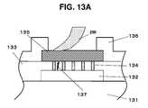
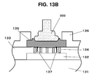
- FIGS. 13 are sectional views for illustrating the related-art semiconductor device.
- a first metal film 132 is formed on an interlayer insulating film 131, and another interlayer insulating film 133 is formed so as to cover the first metal film 132.
- Metal plugs 134 are formed and arranged on the first metal film 132 by known photolithography and etching or by a CMP technology.
- a second metal film 135 is formed above the first metal film 132 so as to be connected to the first metal film 132 via the metal plugs 134.
- a protective film 136 has an opening above the second metal film 135. Further, the protective film 136 covers the second metal film 135 other than at the opening in the protective film 136.
- embedded tungsten plugs are used as the metal plugs 134. All the metal plugs have the same diameter size close to a smallest diameter that can be formed in accordance with a process rule, and a surface of the second metal film 135 is flat (see, for example, Patent Literature 1).
- the present invention has been made in view of the above-mentioned problem, and an object of the present invention is to provide a semiconductor device that can prevent more effectively a crack from developing in an insulating film formed under a bonding pad.
- the present invention uses the following measures.
- a semiconductor device having a bonding pad including: a first metal film formed on a first interlayer insulating film; a second interlayer insulating film formed on the first metal film; a metal plug formed so as to pierce the second interlayer insulating film; and a second metal film formed on the second interlayer insulating film so as to make electrical connection via the metal plug, in which the metal plug includes a first metal plug having a large diameter and a second metal plug having a small diameter, and a surface of the second metal film above the first metal plug has a recessed portion formed therein.
- the first metal plug includes a high melting point metal film and the second metal film
- the second metal plug includes only the high melting point metal film
- a surface of the second metal film directly above the second metal plug is flat.
- the second metal plug is arranged outside a region of the bonding pad.
- the second metal plug is arranged inside a region of the bonding pad.
- the first metal plugs and the second metal plugs are alternately arranged in a region of the bonding pad.
- the metal plugs are arranged in a shape of concentric circles.
- the metal plugs are arranged in a shape of concentric circles, except for directions toward corner portions of the bonding pad.
- the metal plugs are arranged in a shape of a spiral.
- the metal plugs are arranged in a shape of a circle at a center portion of the bonding pad, and further, are arranged in a shape of a spiral outside the circle.
- a plurality of the metal plugs gather to be a trapezoidal region, and four trapezoidal regions are arranged along four sides, respectively, of the bonding pad.
- stress applied to a surface of the bonding pad is dispersed by being moved to the recessed portion formed in the second metal film, which can prevent a crack from developing in the insulating film formed under the bonding pad.
- FIGS. 1 are a plan view and a sectional view for illustrating a semiconductor device according to the present invention.
- FIG. 1(a) is a plan view of the bonding pad.
- a rectangular second metal film 15 is exposed in a region in which a protective film 16 is opened, and, in a rear surface of the second metal film 15, small diameter metal plugs 14a and large diameter metal plugs 14b having a sectional diameter larger than that of the small diameter metal plugs 14a are arranged so as to alternately occupy vertices of a lattice of uniform squares like in a checkerboard.
- the small diameter metal plugs 14a have a diameter size close to a smallest diameter that can be formed in accordance with a process rule. Note that, outside a bonding pad region, only the small diameter metal plugs 14a electrically connect metal wiring in the same layer as that of the second metal film 15 and metal wiring in a lower layer.
- FIG. 1(b) is a sectional view of the bonding pad.
- a rectangular first metal film 12 is formed on a first interlayer insulating film 11 formed on a semiconductor substrate.
- a second interlayer insulating film 13 is formed so as to cover the first metal film 12, and via holes that reach the first metal film 12 are formed in the second interlayer insulating film 13 formed on the first metal film 12.
- the via holes include two kinds of large diameter via holes and small diameter via holes arranged in a mixed manner.
- the small diameter metal plugs 14a are formed in the small diameter via holes, respectively, by filling a barrier metal film and a tungsten film that are formed of a high melting point metal, and the large diameter metal plugs 14b are formed in the large diameter via holes, respectively, by filling the barrier metal film, the tungsten film, and the second metal film 15.
- the second metal film 15 is formed above the first metal film 12 via the second interlayer insulating film 13.
- the first metal film 12 and the second metal film 15 are electrically connected to each other via the large diameter metal plugs 14a and the small diameter metal plugs 14b.
- a lower surface of the second metal film 15 is not flat, and film formation is carried out so that the second metal film 15 enters depressions at centers of the large diameter via holes, respectively, and thus, a front surface of the second metal film 15 is not flat either, and is shaped so as to have recessed portions 17 above the large diameter via holes, that is, above the large diameter metal plugs 14b, respectively.
- the protective film 16 is formed so as to cover end surfaces and side surfaces of the second metal film 15, and the protective film 16 is removed except for the end surfaces of the second metal film 15 so as to have an opening region 18.
- the barrier metal film that is titanium-based is formed by a PVD method, and then, the tungsten film is formed by a CVD method. At this time, the tungsten film is formed at such a thickness so as to completely fill the small diameter via holes and partly fill the large diameter via holes.
- the film formation of complete filling and partial filling as described above can be carried out.
- the tungsten film formed on the second interlayer insulating film 13 is removed by an etching back method or a CMP method.
- the small diameter via holes are completely filled with the barrier metal film and the tungsten film, the large diameter via holes are partly filled therewith, and holes exist at the centers of the large diameter via holes.
- the second metal film 15 is formed by the PVD method, the second metal film 15 enters the large diameter via holes to form the recessed portions in the surface thereof.
- the protective film 16 formed of silicon nitride or the like is formed on the surface of the second metal film 15 and on a surface of the second interlayer insulating film 13, and part of the second metal film 15 is opened, to thereby form the bonding pad (opening region) 18.
- FIG. 1(b) is an illustration of a shape formed by using the etching back method.
- Side walls of tungsten are formed on inner walls of the large diameter via holes, respectively, and the second metal film 15 fills the inside of the side walls. Bottom surfaces of the second metal film 15 are configured to be in direct contact with an upper surface of the first metal film 12.
- the tungsten film in the large diameter via holes is not removed, and thus, the second metal film 15 and the first metal film 12 are configured to be electrically connected to each other via the tungsten film and the barrier metal film.
- Such a bonding pad structure prevents a semiconductor element directly below the bonding pad from being damaged.
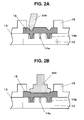
- FIG. 2(a) is an illustration of a state in which the probe needle 200 is in contact with the second metal film 15 in the semiconductor device according to the present invention.
- the probe needle 200 is slid along the surface of the second metal film 15 with a certain amount of pressure in order to enhance its electrical contact with the bonding pad.
- the surface has the recessed portions formed therein, and a tip of the probe needle 200 is fitted into one of the recessed portions and stops. Stress applied in the region propagates through the large diameter metal plug 14b directly therebelow to be dispersed into the first metal film 12. Therefore, excessive stress can be prevented from being applied to the second interlayer insulating film 13, and a crack can be prevented from developing therein.
- FIG. 2(b) is an illustration of a state in which a bonding ball 300 is bonded to the semiconductor device according to the present invention.
- a wire bonding process when a gold ball formed at a tip of a gold wire is pressed against the second metal film 15, the metal film of a protruding portion moves to recessed portions to relax the stress. Specifically, force applied substantially perpendicularly to the surface of the second metal film 15 and an impact of ultrasonic vibrations are horizontally dispersed, and further, are dispersed into the first metal film 12 via the large diameter metal plug 14b to lessen an impact on the second interlayer insulating film 13, to thereby prevent a crack.
- FIGS. 3 to FIG. 12 are illustrations of various modified examples.
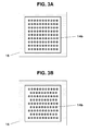
- FIG. 3(a) is a plan view of a semiconductor device in which only the large diameter metal plugs 14b are arranged in the bonding pad.
- the small diameter metal plugs 14a and the large diameter metal plugs 14b having a sectional diameter larger than that of the small diameter metal plugs 14a are arranged so as to alternately occupy vertices of a lattice of uniform squares.
- all the vertices are occupied by the large diameter metal plugs 14b.
- Such a structure increases the number of the recessed portions in the bonding pad region, and increases force to relax the stress, to thereby further reduce impact on a portion under the bonding pad.
- 3(b) is also a plan view of a semiconductor device in which only the large diameter metal plugs 14b are arranged, but the semiconductor device is different from that illustrated in FIG. 3(a) in that the large diameter metal plugs 14b in odd-numbered rows and the large diameter metal plugs 14b in even-numbered rows are arranged so as to be offset from each other. In other words, the large diameter metal plugs 14b are arranged so as to be staggered. In this way, only the large diameter metal plugs 14b are arranged in the bonding pad region, but, outside the bonding pad region, only the small diameter metal plugs 14a electrically connect metal wiring in the same layer as that of the second metal film 15 and metal wiring in a lower layer.
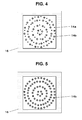
- the large diameter metal plugs 14b and the small diameter metal plugs 14a may be alternately arranged in the shape of concentric circles. Further, as illustrated in FIG. 5 , only the large diameter metal plugs 14b may be arranged. The example illustrated in FIG. 5 has a larger number of the large diameter metal plugs 14b than the example illustrated in FIG. 4 , and thus, the stress is more easily relaxed.
- the metal plugs are concentrically arranged.
- the metal plugs may be arranged in the shape of circles each divided into four, except for corner portions of the bonding pad.
- FIG. 6 is an illustration of a case in which the large diameter metal plugs 14b and the small diameter metal plugs 14a are arranged in a mixed manner
- FIG. 7 is an illustration of a case in which only the large diameter metal plugs 14b are arranged.
- the metal plugs are concentrically arranged.
- the metal plugs may be arranged in the shape of a spiral as the arrangement layout.
- FIG. 8 is an illustration of a case in which the large diameter metal plugs 14b and the small diameter metal plugs 14a are arranged in a mixed manner
- FIG. 9 is an illustration of a case in which only the large diameter metal plugs 14b are arranged. Note that, the direction of the spiral may be clockwise or counterclockwise.
- the large diameter metal plugs 14b may be arranged in the shape of a circle at a center portion of the bonding pad, and further, may be arranged in the shape of a whirlpool outside the circle. Also in this case, the direction of the whirlpool may be clockwise or counterclockwise.
- a plurality of metal plugs gather to be a trapezoidal region, and four such trapezoidal regions are arranged along four sides, respectively, of the bonding pad.
- the small diameter metal plugs 14a are alternately arranged, and, in FIG. 12 , only the large diameter metal plugs 14b are arranged.
Landscapes
- Internal Circuitry In Semiconductor Integrated Circuit Devices (AREA)
- Wire Bonding (AREA)
- Semiconductor Integrated Circuits (AREA)
Abstract
Description
- The present invention relates to a semiconductor device including a bonding pad.
- A related-art semiconductor device including a bonding pad is now described.
FIGS. 13 are sectional views for illustrating the related-art semiconductor device. - When a cross-section in the vicinity of a bonding pad is seen, a
first metal film 132 is formed on aninterlayer insulating film 131, and anotherinterlayer insulating film 133 is formed so as to cover thefirst metal film 132.Metal plugs 134 are formed and arranged on thefirst metal film 132 by known photolithography and etching or by a CMP technology. Asecond metal film 135 is formed above thefirst metal film 132 so as to be connected to thefirst metal film 132 via themetal plugs 134. Aprotective film 136 has an opening above thesecond metal film 135. Further, theprotective film 136 covers thesecond metal film 135 other than at the opening in theprotective film 136. - In this case, embedded tungsten plugs are used as the
metal plugs 134. All the metal plugs have the same diameter size close to a smallest diameter that can be formed in accordance with a process rule, and a surface of thesecond metal film 135 is flat (see, for example, Patent Literature 1). - [PTL 1]
JP 2004-221430 A - However, in the related art, when the
second metal film 135 and thefirst metal film 132 are deformed by stress generated by an impact of aprobe needle 200 or of wire bonding for forming abonding ball 300, the stress concentrates in a downward direction of the bonding pad, and there is a risk in that acrack 137 may develop in theinterlayer insulating film 133. - The present invention has been made in view of the above-mentioned problem, and an object of the present invention is to provide a semiconductor device that can prevent more effectively a crack from developing in an insulating film formed under a bonding pad.
- In order to solve the problem described above, the present invention uses the following measures.
- First, according to one embodiment of the present invention, there is provided a semiconductor device having a bonding pad, including: a first metal film formed on a first interlayer insulating film; a second interlayer insulating film formed on the first metal film; a metal plug formed so as to pierce the second interlayer insulating film; and a second metal film formed on the second interlayer insulating film so as to make electrical connection via the metal plug, in which the metal plug includes a first metal plug having a large diameter and a second metal plug having a small diameter, and a surface of the second metal film above the first metal plug has a recessed portion formed therein.
- Further, in the semiconductor device, the first metal plug includes a high melting point metal film and the second metal film, the second metal plug includes only the high melting point metal film, and a surface of the second metal film directly above the second metal plug is flat.
- Further, in the semiconductor device, the second metal plug is arranged outside a region of the bonding pad.
- Further, in the semiconductor device, the second metal plug is arranged inside a region of the bonding pad.
- Further, in the semiconductor device, the first metal plugs and the second metal plugs are alternately arranged in a region of the bonding pad.
- Further, in the semiconductor device, the metal plugs are arranged in a shape of concentric circles.
- Further, in the semiconductor device, the metal plugs are arranged in a shape of concentric circles, except for directions toward corner portions of the bonding pad.
- Further, in the semiconductor device, the metal plugs are arranged in a shape of a spiral.
- Further, in the semiconductor device, the metal plugs are arranged in a shape of a circle at a center portion of the bonding pad, and further, are arranged in a shape of a spiral outside the circle.
- Further, in the semiconductor device, a plurality of the metal plugs gather to be a trapezoidal region, and four trapezoidal regions are arranged along four sides, respectively, of the bonding pad.
- By using the measures described above, stress applied to a surface of the bonding pad is dispersed by being moved to the recessed portion formed in the second metal film, which can prevent a crack from developing in the insulating film formed under the bonding pad.
-
-
FIGS. 1 are a plan view and a sectional view for illustrating a semiconductor device according to the present invention. -
FIGS. 2 are sectional views in a probe test process and a wire bonding process, respectively, of the semiconductor device according to the present invention. -
FIGS. 3 are plan views for illustrating a semiconductor device according to the present invention. -
FIG. 4 is a plan view for illustrating a semiconductor device according to the present invention. -
FIG. 5 is a plan view for illustrating a semiconductor device according to the present invention. -
FIG. 6 is a plan view for illustrating a semiconductor device according to the present invention. -
FIG. 7 is a plan view for illustrating a semiconductor device according to the present invention. -
FIG. 8 is a plan view for illustrating a semiconductor device according to the present invention. -
FIG. 9 is a plan view for illustrating a semiconductor device according to the present invention. -
FIG. 10 is a plan view for illustrating a semiconductor device according to the present invention. -
FIG. 11 is a plan view for illustrating a semiconductor device according to the present invention. -
FIG. 12 is a plan view for illustrating a semiconductor device according to the present invention. -
FIGS. 13 are sectional views in a probe test process and a wire bonding process, respectively, of a related-art semiconductor device. - An embodiment of the present invention is described with reference to the drawings.
- First, a basic structure of a semiconductor device including a bonding pad is described.
FIGS. 1 are a plan view and a sectional view for illustrating a semiconductor device according to the present invention. -
FIG. 1(a) is a plan view of the bonding pad. A rectangularsecond metal film 15 is exposed in a region in which aprotective film 16 is opened, and, in a rear surface of thesecond metal film 15, smalldiameter metal plugs 14a and largediameter metal plugs 14b having a sectional diameter larger than that of the smalldiameter metal plugs 14a are arranged so as to alternately occupy vertices of a lattice of uniform squares like in a checkerboard. Note that, the smalldiameter metal plugs 14a have a diameter size close to a smallest diameter that can be formed in accordance with a process rule. Note that, outside a bonding pad region, only the smalldiameter metal plugs 14a electrically connect metal wiring in the same layer as that of thesecond metal film 15 and metal wiring in a lower layer. -
FIG. 1(b) is a sectional view of the bonding pad. A rectangularfirst metal film 12 is formed on a first interlayerinsulating film 11 formed on a semiconductor substrate. A secondinterlayer insulating film 13 is formed so as to cover thefirst metal film 12, and via holes that reach thefirst metal film 12 are formed in the secondinterlayer insulating film 13 formed on thefirst metal film 12. The via holes include two kinds of large diameter via holes and small diameter via holes arranged in a mixed manner. The smalldiameter metal plugs 14a are formed in the small diameter via holes, respectively, by filling a barrier metal film and a tungsten film that are formed of a high melting point metal, and the largediameter metal plugs 14b are formed in the large diameter via holes, respectively, by filling the barrier metal film, the tungsten film, and thesecond metal film 15. Thesecond metal film 15 is formed above thefirst metal film 12 via the second interlayerinsulating film 13. Thefirst metal film 12 and thesecond metal film 15 are electrically connected to each other via the largediameter metal plugs 14a and the smalldiameter metal plugs 14b. - As is clear from
FIG. 1(b) , a lower surface of thesecond metal film 15 is not flat, and film formation is carried out so that thesecond metal film 15 enters depressions at centers of the large diameter via holes, respectively, and thus, a front surface of thesecond metal film 15 is not flat either, and is shaped so as to have recessedportions 17 above the large diameter via holes, that is, above the largediameter metal plugs 14b, respectively. Theprotective film 16 is formed so as to cover end surfaces and side surfaces of thesecond metal film 15, and theprotective film 16 is removed except for the end surfaces of thesecond metal film 15 so as to have anopening region 18. - Now, a manufacturing method after the formation of the first metal film is described. After the large diameter via holes and the small diameter via holes are formed in the second
interlayer insulating film 13 using a photolithography technology and an etching technology, the barrier metal film that is titanium-based is formed by a PVD method, and then, the tungsten film is formed by a CVD method. At this time, the tungsten film is formed at such a thickness so as to completely fill the small diameter via holes and partly fill the large diameter via holes. By forming the small diameter via holes to have a diameter that is smaller than twice a sum of a thickness of the barrier metal film and a thickness of the tungsten film and forming the large diameter via holes to have a diameter that is larger than twice the sum of the thickness of the barrier metal film and the thickness of the tungsten film, the film formation of complete filling and partial filling as described above can be carried out. - Then, the tungsten film formed on the second
interlayer insulating film 13 is removed by an etching back method or a CMP method. After the unnecessary tungsten film is removed by the etching back method or the CMP method, in any one of the methods, the small diameter via holes are completely filled with the barrier metal film and the tungsten film, the large diameter via holes are partly filled therewith, and holes exist at the centers of the large diameter via holes. In this state, when thesecond metal film 15 is formed by the PVD method, thesecond metal film 15 enters the large diameter via holes to form the recessed portions in the surface thereof. Then, theprotective film 16 formed of silicon nitride or the like is formed on the surface of thesecond metal film 15 and on a surface of the secondinterlayer insulating film 13, and part of thesecond metal film 15 is opened, to thereby form the bonding pad (opening region) 18. - Further,
FIG. 1(b) is an illustration of a shape formed by using the etching back method. Side walls of tungsten are formed on inner walls of the large diameter via holes, respectively, and thesecond metal film 15 fills the inside of the side walls. Bottom surfaces of thesecond metal film 15 are configured to be in direct contact with an upper surface of thefirst metal film 12. In the case of the CMP method, the tungsten film in the large diameter via holes is not removed, and thus, thesecond metal film 15 and thefirst metal film 12 are configured to be electrically connected to each other via the tungsten film and the barrier metal film. Such a bonding pad structure prevents a semiconductor element directly below the bonding pad from being damaged. - Next, dispersion of stress, which occurs when a probe test or wire bonding is carried out on the semiconductor device according to the present invention, is described.
-
FIG. 2(a) is an illustration of a state in which theprobe needle 200 is in contact with thesecond metal film 15 in the semiconductor device according to the present invention. Theprobe needle 200 is slid along the surface of thesecond metal film 15 with a certain amount of pressure in order to enhance its electrical contact with the bonding pad. In the semiconductor device according to the present invention, the surface has the recessed portions formed therein, and a tip of theprobe needle 200 is fitted into one of the recessed portions and stops. Stress applied in the region propagates through the largediameter metal plug 14b directly therebelow to be dispersed into thefirst metal film 12. Therefore, excessive stress can be prevented from being applied to the secondinterlayer insulating film 13, and a crack can be prevented from developing therein. -
FIG. 2(b) is an illustration of a state in which abonding ball 300 is bonded to the semiconductor device according to the present invention. In a wire bonding process, when a gold ball formed at a tip of a gold wire is pressed against thesecond metal film 15, the metal film of a protruding portion moves to recessed portions to relax the stress. Specifically, force applied substantially perpendicularly to the surface of thesecond metal film 15 and an impact of ultrasonic vibrations are horizontally dispersed, and further, are dispersed into thefirst metal film 12 via the largediameter metal plug 14b to lessen an impact on the secondinterlayer insulating film 13, to thereby prevent a crack. -
FIGS. 3 to FIG. 12 are illustrations of various modified examples. - [Modified Example 1]
FIG. 3(a) is a plan view of a semiconductor device in which only the large diameter metal plugs 14b are arranged in the bonding pad. InFIG. 1(a) , the small diameter metal plugs 14a and the large diameter metal plugs 14b having a sectional diameter larger than that of the small diameter metal plugs 14a are arranged so as to alternately occupy vertices of a lattice of uniform squares. However, in this modified example, all the vertices are occupied by the large diameter metal plugs 14b. Such a structure increases the number of the recessed portions in the bonding pad region, and increases force to relax the stress, to thereby further reduce impact on a portion under the bonding pad.FIG. 3(b) is also a plan view of a semiconductor device in which only the large diameter metal plugs 14b are arranged, but the semiconductor device is different from that illustrated inFIG. 3(a) in that the large diameter metal plugs 14b in odd-numbered rows and the large diameter metal plugs 14b in even-numbered rows are arranged so as to be offset from each other. In other words, the large diameter metal plugs 14b are arranged so as to be staggered. In this way, only the large diameter metal plugs 14b are arranged in the bonding pad region, but, outside the bonding pad region, only the small diameter metal plugs 14a electrically connect metal wiring in the same layer as that of thesecond metal film 15 and metal wiring in a lower layer. - [Modified Example 2] As illustrated in
FIG. 4 , the large diameter metal plugs 14b and the smalldiameter metal plugs 14a may be alternately arranged in the shape of concentric circles. Further, as illustrated inFIG. 5 , only the large diameter metal plugs 14b may be arranged. The example illustrated inFIG. 5 has a larger number of the large diameter metal plugs 14b than the example illustrated inFIG. 4 , and thus, the stress is more easily relaxed. - [Modified Example 3] In the case illustrated in
FIG. 4 , the metal plugs are concentrically arranged. As illustrated inFIG. 6 , the metal plugs may be arranged in the shape of circles each divided into four, except for corner portions of the bonding pad.FIG. 6 is an illustration of a case in which the large diameter metal plugs 14b and the small diameter metal plugs 14a are arranged in a mixed manner, andFIG. 7 is an illustration of a case in which only the large diameter metal plugs 14b are arranged. - [Modified Example 4] In the case illustrated in
FIG. 4 , the metal plugs are concentrically arranged. As illustrated inFIG. 8 , the metal plugs may be arranged in the shape of a spiral as the arrangement layout.FIG. 8 is an illustration of a case in which the large diameter metal plugs 14b and the small diameter metal plugs 14a are arranged in a mixed manner, andFIG. 9 is an illustration of a case in which only the large diameter metal plugs 14b are arranged. Note that, the direction of the spiral may be clockwise or counterclockwise. - [Modified Example 5] As illustrated in
FIG. 10 , the large diameter metal plugs 14b may be arranged in the shape of a circle at a center portion of the bonding pad, and further, may be arranged in the shape of a whirlpool outside the circle. Also in this case, the direction of the whirlpool may be clockwise or counterclockwise. - [Modified Example 6] In
FIG. 11 andFIG. 12 , a plurality of metal plugs gather to be a trapezoidal region, and four such trapezoidal regions are arranged along four sides, respectively, of the bonding pad. InFIG. 11 , the small diameter metal plugs 14a are alternately arranged, and, inFIG. 12 , only the large diameter metal plugs 14b are arranged. With such a structure, stress of deformation and movement of the second metal film due to an impact in a direction in which ultrasonic vibrations of the bonding are caused is more easily relaxed by the influence of the recessed portions, and stress due to an impact in a direction of entrance of the probe is more easily relaxed. -
- 11
- first interlayer insulating film
- 13
- second interlayer insulating film
- 12
- first metal film
- 14a
- large diameter metal plug
- 14b
- small diameter metal plug
- 15
- second metal film
- 16
- protective film
- 17
- recessed portion
- 18
- bonding pad (opening region)
- 131
- first interlayer insulating film
- 133
- second interlayer insulating film
- 132
- first metal film
- 134
- small diameter metal plug
- 135
- second metal film
- 136
- protective film
- 137
- crack
- 200
- probe needle
- 300
- bonding ball
Claims (10)
- A semiconductor device having a bonding pad, comprising:a first metal film formed on a first interlayer insulating film;a second interlayer insulating film formed on the first metal film;a metal plug formed so as to pierce the second interlayer insulating film; andthe bonding pad formed on the second interlayer insulating film so as to make electrical connection via the metal plug, the bonding pad being formed of a second metal film,wherein the metal plug comprises a first metal plug having a large diameter, andwherein the second metal film enters the first metal plug so that a surface of the bonding pad directly above the first metal plug has a recessed portion formed therein.
- A semiconductor device according to claim 1, wherein the metal plug further comprises a second metal plug having a diameter smaller than the diameter of the first metal plug.
- A semiconductor device according to claim 2,
wherein the first metal plug comprises a high melting point metal film and the second metal film,
wherein the second metal plug comprises only the high melting point metal film, and wherein a surface of the second metal film directly above the second metal plug is flat. - A semiconductor device according to claim 2 or 3, wherein the second metal plug is arranged outside a region of the bonding pad.
- A semiconductor device according to any one of claims 2 to 4, wherein the first metal plugs and the second metal plugs are alternately arranged in a region of the bonding pad.
- A semiconductor device according to any one of claims 1 to 5, wherein the metal plugs are arranged in a shape of concentric circles in a region of the bonding pad.
- A semiconductor device according to any one of claims 1 to 5, wherein the metal plugs are arranged in a shape of concentric circles in a region of the bonding pad, except for directions toward corner portions of the bonding pad.
- A semiconductor device according to any one of claims 1 to 5, wherein the metal plugs are arranged in a shape of a spiral in a region of the bonding pad.
- A semiconductor device according to any one of claims 1 to 5, wherein the metal plugs are arranged in a shape of a circle at a center portion of the bonding pad, and further, are arranged in a shape of a whirlpool outside the circle.
- A semiconductor device according to any one of claims 1 to 5, wherein a plurality of the metal plugs gather to be a trapezoidal region and four trapezoidal regions are arranged along four sides, respectively, of the bonding pad in a region of the bonding pad.
Applications Claiming Priority (2)
| Application Number | Priority Date | Filing Date | Title |
|---|---|---|---|
| JP2013018754A JP6027452B2 (en) | 2013-02-01 | 2013-02-01 | Semiconductor device |
| PCT/JP2014/050192 WO2014119348A1 (en) | 2013-02-01 | 2014-01-09 | Semiconductor device |
Publications (2)
| Publication Number | Publication Date |
|---|---|
| EP2953159A1 true EP2953159A1 (en) | 2015-12-09 |
| EP2953159A4 EP2953159A4 (en) | 2016-11-09 |
Family
ID=51262063
Family Applications (1)
| Application Number | Title | Priority Date | Filing Date |
|---|---|---|---|
| EP14746692.4A Withdrawn EP2953159A4 (en) | 2013-02-01 | 2014-01-09 | SEMICONDUCTOR DEVICE |
Country Status (7)
| Country | Link |
|---|---|
| US (1) | US9412710B2 (en) |
| EP (1) | EP2953159A4 (en) |
| JP (1) | JP6027452B2 (en) |
| KR (1) | KR102145168B1 (en) |
| CN (1) | CN104969334B (en) |
| TW (1) | TWI604581B (en) |
| WO (1) | WO2014119348A1 (en) |
Families Citing this family (7)
| Publication number | Priority date | Publication date | Assignee | Title |
|---|---|---|---|---|
| CN105489582B (en) * | 2015-12-29 | 2018-09-28 | 苏州晶方半导体科技股份有限公司 | Semiconductor chip and forming method thereof |
| JP6548825B2 (en) * | 2015-12-29 | 2019-07-24 | チャイナ ウェイファー レベル シーエスピー カンパニー リミテッド | Solder pad, semiconductor chip including solder pad and method of forming the same |
| CN108666287B (en) * | 2017-04-01 | 2020-07-28 | 中芯国际集成电路制造(北京)有限公司 | Pad structure |
| CN109422234B (en) * | 2017-09-01 | 2021-04-09 | 中芯国际集成电路制造(上海)有限公司 | Test structure and method of making the same |
| CN111863787B (en) * | 2019-04-29 | 2022-05-24 | 群创光电股份有限公司 | Electronic device with a detachable cover |
| CN110310920A (en) * | 2019-07-03 | 2019-10-08 | 上海华虹宏力半导体制造有限公司 | Semiconductor devices and preparation method thereof |
| KR20240107839A (en) * | 2022-12-30 | 2024-07-09 | 엘지이노텍 주식회사 | Semiconductor package |
Family Cites Families (17)
| Publication number | Priority date | Publication date | Assignee | Title |
|---|---|---|---|---|
| US5248903A (en) * | 1992-09-18 | 1993-09-28 | Lsi Logic Corporation | Composite bond pads for semiconductor devices |
| US6300688B1 (en) * | 1994-12-07 | 2001-10-09 | Quicklogic Corporation | Bond pad having vias usable with antifuse process technology |
| US5665996A (en) * | 1994-12-30 | 1997-09-09 | Siliconix Incorporated | Vertical power mosfet having thick metal layer to reduce distributed resistance |
| JPH08293523A (en) * | 1995-02-21 | 1996-11-05 | Seiko Epson Corp | Semiconductor device and manufacturing method thereof |
| US6110816A (en) * | 1999-03-05 | 2000-08-29 | Taiwan Semiconductor Manufacturing Company | Method for improving bondability for deep-submicron integrated circuit package |
| JP2002118268A (en) * | 2000-10-10 | 2002-04-19 | Matsushita Electric Ind Co Ltd | Semiconductor device and method of connecting to semiconductor device |
| KR100437460B1 (en) * | 2001-12-03 | 2004-06-23 | 삼성전자주식회사 | Semiconductor device having bonding pads and fabrication method thereof |
| JP2003347351A (en) * | 2002-05-29 | 2003-12-05 | Mitsubishi Electric Corp | Semiconductor device |
| JP3970150B2 (en) * | 2002-10-16 | 2007-09-05 | 三洋電機株式会社 | Bonding pad and method for forming the same |
| JP4092214B2 (en) | 2003-01-16 | 2008-05-28 | Necエレクトロニクス株式会社 | Semiconductor device |
| JP2005116562A (en) * | 2003-10-02 | 2005-04-28 | Renesas Technology Corp | Semiconductor device |
| JP4674522B2 (en) * | 2004-11-11 | 2011-04-20 | 株式会社デンソー | Semiconductor device |
| KR20080067129A (en) * | 2007-01-15 | 2008-07-18 | 삼성전자주식회사 | Semiconductor device with multilayer pads |
| JP5329068B2 (en) * | 2007-10-22 | 2013-10-30 | ルネサスエレクトロニクス株式会社 | Semiconductor device |
| JP5205066B2 (en) * | 2008-01-18 | 2013-06-05 | ルネサスエレクトロニクス株式会社 | Semiconductor device and manufacturing method thereof |
| JP2012195328A (en) * | 2011-03-15 | 2012-10-11 | Panasonic Corp | Semiconductor device and manufacturing method of the same |
| US8994181B2 (en) * | 2011-08-18 | 2015-03-31 | Taiwan Semiconductor Manufacturing Company, Ltd. | Bond pad structure to reduce bond pad corrosion |
-
2013
- 2013-02-01 JP JP2013018754A patent/JP6027452B2/en not_active Expired - Fee Related
-
2014
- 2014-01-09 CN CN201480007251.0A patent/CN104969334B/en not_active Expired - Fee Related
- 2014-01-09 EP EP14746692.4A patent/EP2953159A4/en not_active Withdrawn
- 2014-01-09 US US14/762,497 patent/US9412710B2/en not_active Expired - Fee Related
- 2014-01-09 WO PCT/JP2014/050192 patent/WO2014119348A1/en not_active Ceased
- 2014-01-09 KR KR1020157020908A patent/KR102145168B1/en not_active Expired - Fee Related
- 2014-01-15 TW TW103101421A patent/TWI604581B/en not_active IP Right Cessation
Also Published As
| Publication number | Publication date |
|---|---|
| CN104969334B (en) | 2017-06-16 |
| CN104969334A (en) | 2015-10-07 |
| JP2014150190A (en) | 2014-08-21 |
| JP6027452B2 (en) | 2016-11-16 |
| US20150357297A1 (en) | 2015-12-10 |
| WO2014119348A1 (en) | 2014-08-07 |
| KR102145168B1 (en) | 2020-08-18 |
| EP2953159A4 (en) | 2016-11-09 |
| KR20150112990A (en) | 2015-10-07 |
| TW201438167A (en) | 2014-10-01 |
| US9412710B2 (en) | 2016-08-09 |
| TWI604581B (en) | 2017-11-01 |
Similar Documents
| Publication | Publication Date | Title |
|---|---|---|
| US9412710B2 (en) | Semiconductor device | |
| CN106548996B (en) | Pseudo-metal with jagged edges | |
| CN103946962B (en) | The manufacture method of semiconductor device | |
| US9053973B2 (en) | Semiconductor device | |
| JP2016032102A (en) | Package substrate | |
| JP2008258258A (en) | Semiconductor device | |
| US8791578B2 (en) | Through-silicon via structure with patterned surface, patterned sidewall and local isolation | |
| TW201611225A (en) | Semiconductor device | |
| US12593737B2 (en) | Semiconductor package | |
| CN106898589A (en) | Integrated circuit with a plurality of transistors | |
| CN109422234A (en) | Test structure and its manufacturing method | |
| CN109273429A (en) | Semiconductor device with a plurality of semiconductor chips | |
| US10340229B2 (en) | Semiconductor device with superior crack resistivity in the metallization system | |
| CN105489581A (en) | Semiconductor structure and fabrication method thereof | |
| CN102097393B (en) | Semiconductor device | |
| CN104851875B (en) | Semiconductor structure with through silicon via and manufacturing method and testing method thereof | |
| CN113437042B (en) | Pad structure, semiconductor test structure and semiconductor test method | |
| CN109411407B (en) | A semiconductor device and method of making the same | |
| US9111755B1 (en) | Bond pad and passivation layer having a gap and method for forming | |
| TWI587418B (en) | Semiconductor device and method of manufacturing same | |
| KR101115455B1 (en) | Semiconductor device | |
| KR20200086411A (en) | Semiconductor device | |
| KR20250066371A (en) | Semiconductor package | |
| CN107871668A (en) | Bonding pad structure and manufacturing method thereof | |
| CN115425008A (en) | Semiconductor structure |
Legal Events
| Date | Code | Title | Description |
|---|---|---|---|
| PUAI | Public reference made under article 153(3) epc to a published international application that has entered the european phase |
Free format text: ORIGINAL CODE: 0009012 |
|
| 17P | Request for examination filed |
Effective date: 20150901 |
|
| AK | Designated contracting states |
Kind code of ref document: A1 Designated state(s): AL AT BE BG CH CY CZ DE DK EE ES FI FR GB GR HR HU IE IS IT LI LT LU LV MC MK MT NL NO PL PT RO RS SE SI SK SM TR |
|
| AX | Request for extension of the european patent |
Extension state: BA ME |
|
| RAP1 | Party data changed (applicant data changed or rights of an application transferred) |
Owner name: SEIKO INSTRUMENTS INC. |
|
| RAP1 | Party data changed (applicant data changed or rights of an application transferred) |
Owner name: SII SEMICONDUCTOR CORPORATION |
|
| DAX | Request for extension of the european patent (deleted) | ||
| A4 | Supplementary search report drawn up and despatched |
Effective date: 20161010 |
|
| RIC1 | Information provided on ipc code assigned before grant |
Ipc: H01L 21/60 20060101ALI20161004BHEP Ipc: H01L 23/522 20060101ALI20161004BHEP Ipc: H01L 21/3205 20060101AFI20161004BHEP Ipc: H01L 21/768 20060101ALI20161004BHEP |
|
| RIN1 | Information on inventor provided before grant (corrected) |
Inventor name: YAMAMOTO, SUKEHIRO |
|
| RAP1 | Party data changed (applicant data changed or rights of an application transferred) |
Owner name: ABLIC INC. |
|
| STAA | Information on the status of an ep patent application or granted ep patent |
Free format text: STATUS: THE APPLICATION HAS BEEN WITHDRAWN |
|
| 18W | Application withdrawn |
Effective date: 20201023 |