EP2950328A1 - Suction apparatus, carry-in method, conveyance system, light exposure device, and device production method - Google Patents
Suction apparatus, carry-in method, conveyance system, light exposure device, and device production method Download PDFInfo
- Publication number
- EP2950328A1 EP2950328A1 EP13858330.7A EP13858330A EP2950328A1 EP 2950328 A1 EP2950328 A1 EP 2950328A1 EP 13858330 A EP13858330 A EP 13858330A EP 2950328 A1 EP2950328 A1 EP 2950328A1
- Authority
- EP
- European Patent Office
- Prior art keywords
- suction
- wafer
- section
- carrier system
- gas
- Prior art date
- Legal status (The legal status is an assumption and is not a legal conclusion. Google has not performed a legal analysis and makes no representation as to the accuracy of the status listed.)
- Withdrawn
Links
Images


Classifications
-
- H—ELECTRICITY
- H01—ELECTRIC ELEMENTS
- H01L—SEMICONDUCTOR DEVICES NOT COVERED BY CLASS H10
- H01L21/00—Processes or apparatus adapted for the manufacture or treatment of semiconductor or solid state devices or of parts thereof
- H01L21/67—Apparatus specially adapted for handling semiconductor or electric solid state devices during manufacture or treatment thereof; Apparatus specially adapted for handling wafers during manufacture or treatment of semiconductor or electric solid state devices or components ; Apparatus not specifically provided for elsewhere
- H01L21/683—Apparatus specially adapted for handling semiconductor or electric solid state devices during manufacture or treatment thereof; Apparatus specially adapted for handling wafers during manufacture or treatment of semiconductor or electric solid state devices or components ; Apparatus not specifically provided for elsewhere for supporting or gripping
- H01L21/6838—Apparatus specially adapted for handling semiconductor or electric solid state devices during manufacture or treatment thereof; Apparatus specially adapted for handling wafers during manufacture or treatment of semiconductor or electric solid state devices or components ; Apparatus not specifically provided for elsewhere for supporting or gripping with gripping and holding devices using a vacuum; Bernoulli devices
-
- B—PERFORMING OPERATIONS; TRANSPORTING
- B25—HAND TOOLS; PORTABLE POWER-DRIVEN TOOLS; MANIPULATORS
- B25J—MANIPULATORS; CHAMBERS PROVIDED WITH MANIPULATION DEVICES
- B25J11/00—Manipulators not otherwise provided for
- B25J11/0095—Manipulators transporting wafers
-
- G—PHYSICS
- G03—PHOTOGRAPHY; CINEMATOGRAPHY; ANALOGOUS TECHNIQUES USING WAVES OTHER THAN OPTICAL WAVES; ELECTROGRAPHY; HOLOGRAPHY
- G03F—PHOTOMECHANICAL PRODUCTION OF TEXTURED OR PATTERNED SURFACES, e.g. FOR PRINTING, FOR PROCESSING OF SEMICONDUCTOR DEVICES; MATERIALS THEREFOR; ORIGINALS THEREFOR; APPARATUS SPECIALLY ADAPTED THEREFOR
- G03F7/00—Photomechanical, e.g. photolithographic, production of textured or patterned surfaces, e.g. printing surfaces; Materials therefor, e.g. comprising photoresists; Apparatus specially adapted therefor
- G03F7/70—Microphotolithographic exposure; Apparatus therefor
- G03F7/70691—Handling of masks or workpieces
- G03F7/70733—Handling masks and workpieces, e.g. exchange of workpiece or mask, transport of workpiece or mask
-
- G—PHYSICS
- G03—PHOTOGRAPHY; CINEMATOGRAPHY; ANALOGOUS TECHNIQUES USING WAVES OTHER THAN OPTICAL WAVES; ELECTROGRAPHY; HOLOGRAPHY
- G03F—PHOTOMECHANICAL PRODUCTION OF TEXTURED OR PATTERNED SURFACES, e.g. FOR PRINTING, FOR PROCESSING OF SEMICONDUCTOR DEVICES; MATERIALS THEREFOR; ORIGINALS THEREFOR; APPARATUS SPECIALLY ADAPTED THEREFOR
- G03F7/00—Photomechanical, e.g. photolithographic, production of textured or patterned surfaces, e.g. printing surfaces; Materials therefor, e.g. comprising photoresists; Apparatus specially adapted therefor
- G03F7/70—Microphotolithographic exposure; Apparatus therefor
- G03F7/708—Construction of apparatus, e.g. environment aspects, hygiene aspects or materials
- G03F7/70908—Hygiene, e.g. preventing apparatus pollution, mitigating effect of pollution or removing pollutants from apparatus
-
- H—ELECTRICITY
- H01—ELECTRIC ELEMENTS
- H01L—SEMICONDUCTOR DEVICES NOT COVERED BY CLASS H10
- H01L21/00—Processes or apparatus adapted for the manufacture or treatment of semiconductor or solid state devices or of parts thereof
- H01L21/67—Apparatus specially adapted for handling semiconductor or electric solid state devices during manufacture or treatment thereof; Apparatus specially adapted for handling wafers during manufacture or treatment of semiconductor or electric solid state devices or components ; Apparatus not specifically provided for elsewhere
- H01L21/677—Apparatus specially adapted for handling semiconductor or electric solid state devices during manufacture or treatment thereof; Apparatus specially adapted for handling wafers during manufacture or treatment of semiconductor or electric solid state devices or components ; Apparatus not specifically provided for elsewhere for conveying, e.g. between different workstations
- H01L21/67739—Apparatus specially adapted for handling semiconductor or electric solid state devices during manufacture or treatment thereof; Apparatus specially adapted for handling wafers during manufacture or treatment of semiconductor or electric solid state devices or components ; Apparatus not specifically provided for elsewhere for conveying, e.g. between different workstations into and out of processing chamber
- H01L21/67751—Apparatus specially adapted for handling semiconductor or electric solid state devices during manufacture or treatment thereof; Apparatus specially adapted for handling wafers during manufacture or treatment of semiconductor or electric solid state devices or components ; Apparatus not specifically provided for elsewhere for conveying, e.g. between different workstations into and out of processing chamber vertical transfer of a single workpiece
-
- H—ELECTRICITY
- H01—ELECTRIC ELEMENTS
- H01L—SEMICONDUCTOR DEVICES NOT COVERED BY CLASS H10
- H01L21/00—Processes or apparatus adapted for the manufacture or treatment of semiconductor or solid state devices or of parts thereof
- H01L21/67—Apparatus specially adapted for handling semiconductor or electric solid state devices during manufacture or treatment thereof; Apparatus specially adapted for handling wafers during manufacture or treatment of semiconductor or electric solid state devices or components ; Apparatus not specifically provided for elsewhere
- H01L21/683—Apparatus specially adapted for handling semiconductor or electric solid state devices during manufacture or treatment thereof; Apparatus specially adapted for handling wafers during manufacture or treatment of semiconductor or electric solid state devices or components ; Apparatus not specifically provided for elsewhere for supporting or gripping
- H01L21/687—Apparatus specially adapted for handling semiconductor or electric solid state devices during manufacture or treatment thereof; Apparatus specially adapted for handling wafers during manufacture or treatment of semiconductor or electric solid state devices or components ; Apparatus not specifically provided for elsewhere for supporting or gripping using mechanical means, e.g. chucks, clamps or pinches
- H01L21/68714—Apparatus specially adapted for handling semiconductor or electric solid state devices during manufacture or treatment thereof; Apparatus specially adapted for handling wafers during manufacture or treatment of semiconductor or electric solid state devices or components ; Apparatus not specifically provided for elsewhere for supporting or gripping using mechanical means, e.g. chucks, clamps or pinches the wafers being placed on a susceptor, stage or support
- H01L21/68742—Apparatus specially adapted for handling semiconductor or electric solid state devices during manufacture or treatment thereof; Apparatus specially adapted for handling wafers during manufacture or treatment of semiconductor or electric solid state devices or components ; Apparatus not specifically provided for elsewhere for supporting or gripping using mechanical means, e.g. chucks, clamps or pinches the wafers being placed on a susceptor, stage or support characterised by a lifting arrangement, e.g. lift pins
Definitions
- the present invention relates to suction devices, carry-in methods, carrier systems and exposure apparatuses, and device manufacturing methods, and more particularly to a suction device in which its suction force acts in a non-contact manner on a plate-like object, a carry-in method in which carry-in is performed of the plate-like object onto a movable body, a carrier system suitable for carrying out the carry-in method and an exposure apparatus which is equipped with the carrier system, and a device manufacturing method which uses the exposure apparatus.
- a projection exposure apparatus of a step-and-repeat method a so-called stepper
- projection exposure apparatus of a step-and-scan method a so-called scanning stepper (also called a scanner) or the like is mainly used.
- Substrates such as a wafer, a glass plate and the like subject to exposure that are used in these types of exposure apparatuses are gradually becoming larger (for example, in the case of a wafer, in every ten years).
- a 300-mm wafer which has a diameter of 300mm is currently the mainstream, the coming of age of a 450mm wafer which has a diameter of 450mm looms near.
- the transition to 450mm wafers occurs, the number of dies (chips) output from a single wafer becomes double or more than the number of chips from the current 300mm wafer, which contributes to reducing the cost.
- the 450mm wafer is extremely weak in intensity and rigidity when compared with the 300mm wafer. Therefore, when focusing on a point such as a carriage of a wafer, it was considered that there was a risk of warping occurring in the wafer, which may negatively effect the exposure accuracy when a means method similar to the current 300mm wafer was employed.
- a carry-in method of the wafer a proposal is made of a carry-in method or the like that can be employed even when the wafer is a 450mm wafer in which the wafer is suctioned from above in a non-contact manner by a carrier member equipped with a Bernoulli chuck or the like to maintain the flatness degree (flatness) and performs carry-in onto a wafer holder (holding device) (for example, refer to PTL 1).
- a method for resolving the inconvenience due to suction in a non-contact manner from above by the wafer carrier member described above a method can be considered in which while a wafer is suctioned in a non-contact manner suction from above by a Bernoulli chuck or the like, the wafer is also supported from below by a support section (for example, vertical-motion pins on a wafer stage).
- a support section for example, vertical-motion pins on a wafer stage
- a first suction device in which a suction force is made to act on a plate-like object in a non-contact manner, comprising: a base member; and a plurality of suction members provided at the base member that each generates a gas flow around the obj ect to make a force which suctions the obj ect, wherein the plurality of suction members generate the gas flow in a mutually different state.
- the suction force with respect to the object generated by each of the plurality of suction members can be made different according to, for example, the position on the base member of each suction member. Therefore, for example, in the case of performing support of the object from below by the support section and suction in a non-contact manner from above of the object by this suction device, it becomes possible to make the suction force generated by the suction members placed at a part facing the support section of the base member be weaker than the suction force generated by the suction members placed at a part which does not face the support section of the base member.
- a second suction device in which a suction force is made to act on a plate-like object in a non-contact manner, comprising: a base member; a plurality of gas flow holes provided at the base member that each generates a gas flow around the object; and an adjustment device which deforms the object, wherein the object is deformed by the adjustment device while the object is held by the gas flow via the plurality of gas flow holes.
- the adjustment device while holding the object by the gas flow via the plurality of gas flow holes, it becomes possible for the adjustment device to deform the object, for example, so that a desired level of flatness is secured.
- a carry-in method in which carry-in of a plate-like object onto a holding member having an object mounting surface provided on its upper surface is performed, the method comprising: carrying the object above the object mounting surface of the holding member at a predetermined carry-in position; suctioning a surface of the object from above by a suction member in a non-contact manner; supporting from below a part of a center section area at an other surface on an opposite side of the surface of the object suctioned by the suction member by a vertically movable support section provided at the holding member, and weakening a suction force by the suction member with respect to an area of the surface of the object corresponding to the center section area including a supporting point by the support section; and driving the suction member and the support section downward toward the object mounting surface, in a state maintaining a suction state by the suction member and a support state by the support section with respect to the object.
- a carrier system in which a plate-like object is carried, comprising: a holding member in which an object mounting surface is provided at its upper surface; a vertically movable suction member provided above the holding member at a predetermined carry-in position, the suction member being able to suction a plurality of places including at least an area at an outer circumference section of a surface of the object from above in a non-contact manner; a support section provided at the holding member, the support section being vertically movable and can support from below a part of the center section area at an other surface on an opposite side of the surface of the object; and a driving device which drives the suction member and the support section downward so that the other surface of the object moves toward the object mounting surface of the holding member, in a state where a suction state by the suction member and a support state by the support section with respect to the object is maintained.
- a first exposure apparatus which forms a pattern on an object, comprising: the suction device related to any of the first and second aspects described above; and a pattern generating device in which the pattern is formed by exposing the object suctioned by the suction device and carried in on the holding member with an energy beam.
- a second exposure apparatus which forms a pattern on an object, comprising: the carrier system described above; and a pattern generating device in which the pattern is formed by exposing the object carried in on the holding member by the carrier system with an energy beam.
- a device manufacturing method including: exposing an object using the exposure apparatus described above; and developing the object which has been exposed.
- FIG. 1 schematically shows a structure of an exposure apparatus 100 related to an embodiment.
- This exposure apparatus 100 is a projection exposure apparatus of a step-and-scan method, or a so-called scanner.
- a projection optical system PL is arranged in the present embodiment, and in the description below, a direction parallel to an optical axis AX of this projection optical system PL will be described as a Z-axis direction, a direction within a plane orthogonal to the Z-axis direction in which a reticle R and a wafer W are relatively scanned will be described as the Y-axis direction, a direction orthogonal to the Z-axis and the Y-axis will be described as an X-axis direction, and rotational (inclination) direction around the X-axis, the Y-axis, and the Z-axis will be described as a ⁇ x direction, a ⁇ y direction, and a ⁇ z direction.
- Exposure apparatus 100 is equipped with an illumination system 10, a reticle stage RST which holds reticle (mask) R, projection optical system PL, a wafer stage WST which holds wafer W, a carry-in unit 121 which structures a wafer carrier system 120 (refer to FIG. 4 ) along with a carry-out unit which is not shown and a vertical-motion pin which will be described later on, and a control system or the like of these parts.
- Illumination system 10 includes a light source, an illuminance equalizing optical system including an optical integrator and the like, and an illumination optical system that has a reticle blind and the like (none of which are shown) .
- Illumination system 10 illuminates a slit-shaped illumination area IAR set (limited) on reticle R by the reticle blind (also called a masking system) by an illumination light (exposure light) IL, with a substantially uniform illuminance.
- illumination light IL for example, an ArF excimer laser beam (wavelength 193nm) is used.
- Reticle stage RST On reticle stage RST, reticle R on which a circuit pattern or the like is formed on its pattern surface (the lower surface in FIG. 1 ) is fixed, for example, by vacuum chucking.
- Reticle stage RST for example, is finely drivable within the XY plane by a reticle stage driving system 11 (not shown in FIG. 1 , refer to FIG. 4 ) including a linear motor, a planar motor or the like, and is also drivable in a scanning direction (the Y-axis direction which is the lateral direction of the page surface in FIG. 1 ) at a predetermined scanning speed.
- Position information (including rotation information in the ⁇ z direction) of reticle stage RST in the XY plane is constantly detected, for example, by a reticle laser interferometer (hereinafter, referred to as a "reticle interferometer") 13, via a movable mirror 15 (actually, a Y movable mirror (or a retroreflector) having a reflection surface orthogonal to the Y-axis direction and an X movable mirror having a reflection surface orthogonal to the X-axis direction are provided) fixed to reticle stage RST, at a resolution of, for example, around 0.25nm.
- Measurement values of reticle interferometer 13 are sent to a main controller 20 (not shown in FIG. 1 , refer to FIG.
- Main controller 20 drives reticle stage RST via reticle stage driving system 11 (refer to FIG. 4 ), based on the position information of reticle stage RST.
- position information of reticle stage RST in the XY plane can be detected using an encoder, instead of the reticle interferometer described above.
- Projection optical system PL is placed below reticle stage RST in FIG. 1 .
- Projection optical system PL is mounted on a main frame BD supported horizontally by a support member which is not shown.
- projection optical system PL for example, is a dioptric system consisting of a plurality of optical elements (lens elements) arranged along optical axis AX, which is parallel to the Z-axis.
- Projection optical system PL for example, is double telecentric, and has a predetermined projection magnification (for example, 1/4 times, 1/5 times or 1/8 times).
- illumination area IAR on reticle R is illuminated by illumination light IL from illumination system 10
- a reduced image of the circuit pattern of reticle R (a reduced image of a part of the circuit pattern) within illumination area IAR is formed in an area (hereinafter, also called an exposure area) IA conjugate to illumination area IAR on wafer W whose surface is coated with a resist (sensitive agent) and is placed on a second surface (image plane) side of projection optical system PL, via projection optical system PL, by illumination light IL having passed through reticle R placed so that its pattern surface substantially coincides with a first surface (object plane) of projection optical system PL.
- reticle stage RST and wafer stage WST (to be more precise, fine movement stage WFS to be described later on which holds wafer W) being synchronously driven, scanning exposure of a shot area (divided area) on wafer W is performed, by reticle R being relatively moved in the scanning direction (Y-axis direction) with respect to illumination area IAR (illumination light IL) and wafer W being relatively moved in the scanning direction (Y-axis direction) with respect to exposure area IA (illumination light IL), and the pattern of reticle R is transferred onto the shot area.
- illumination area IAR illumination light IL
- wafer W being relatively moved in the scanning direction (Y-axis direction) with respect to exposure area IA (illumination light IL)
- the pattern of reticle R is generated on wafer W by illumination system 10 and projection optical system PL, and by the exposure of the sensitive layer (resist layer) on wafer W with illumination light IL the pattern is formed on wafer W.
- Wafer stage WST is supported by levitation on base board 12, via air bearings which will be described later on.
- base board 12 is supported almost horizontally (parallel to the XY plane) on a floor F by a vibration-proof mechanism (omitted in drawings).
- Base board 12 consists of a member that has a flat plate-like outer shape.
- a coil unit is housed, which includes a plurality of coils 17 placed in the shape of a matrix with the XY two-dimensional direction serving as a row direction and a column direction.
- Wafer stage WST has a coarse movement stage WCS, and a fine movement stage WFS, which is supported in a non-contact state by coarse movement stage and is relatively movable with respect to coarse movement stage WCS.
- wafer stage WST (coarse movement stage WCS) is driven in predetermined strokes in the X-axis direction and the Y-axis direction, and is also finely driven in the ⁇ z direction by a coarse movement stage driving system 51 (refer to FIG. 4 ).
- fine movement stage WFS is driven in directions of six degrees of freedom (the X-axis direction, the Y-axis direction, the Z-axis direction, the ⁇ x direction, the ⁇ y direction and the ⁇ z direction) by a fine movement stage driving system 52 (refer to FIG. 4 ), with respect to coarse movement stage WCS.
- Coarse movement stage WCS is equipped with a coarse movement slider section 91 having a rectangular plate-like shape whose length in the X-axis direction is slightly longer than the length in the Y-axis direction in a planar view (when viewed from the +Z direction), a pair of side wall sections 92a, 92b, each having a rectangular plate-like shape with the longitudinal direction being the Y-axis direction, and being fixed on the upper surface of one end and the other end of coarse movement slider section 91 in the longitudinal direction in a state parallel to the YZ plane, and a pair of stator sections 93a, 93b fixed on the upper surface of side wall sections 92a, 92b, respectively, at the center in the Y-axis direction facing the inner side.
- Coarse movement stage WCS has a low height rectangular parallelepiped shape whose upper surface is open at the center in the X-axis direction and on both sides in the Y-axis direction. That is, in coarse movement stage WCS, a space section penetrating in the Y-axis direction is formed inside.
- side wall sections 92a, 92b can have almost the same length in the Y-axis direction as stator sections 93a, 93b. That is, side wall sections 92a, 92b may be provided only at the center in the Y-axis direction on the upper surface of coarse movement slider section 91, at one end and the other end in the longitudinal direction.
- a magnet unit corresponding to the coil unit placed inside base board 12 consisting of a plurality of permanent magnets 18 placed in the shape of a matrix with the XY two-dimensional directions serving as a row direction and the column direction.
- the magnet unit along with the coil unit of base board 12, structures coarse movement stage driving system 51 (refer to FIG. 4 ) consisting of a planar motor of an electromagnetic force (Lorentz force) driving method whose details are disclosed, for example, in U.S. Patent No. 5,196,745 and the like.
- the magnitude and direction of the electric current supplied to each coil 17 structuring the coil unit are controlled by main controller 20.
- a plurality of air bearings 94 is fixed around the magnet unit described above.
- Coarse movement stage WCS is supported by levitation by the plurality of air bearings 94, via a predetermined gap (clearance, gap) above base board 12, such as for example, a gap of about several ⁇ m, and is driven in the X-axis direction, the Y-axis direction and the ⁇ z direction by coarse movement stage driving system 51.
- coarse movement stage driving system 51 is not limited to the planar motor of the electromagnetic force (Lorentz force) driving method, and for example, a planar motor of a variable magneto-resistance driving method can also be used.
- coarse movement stage driving system 51 can be structured by a magnetic levitation type planar motor, and the planar motor can driving coarse movement stage WCS in directions of six degrees of freedom. In this case, the air bearings will not have to be arranged at the bottom surface of coarse movement slider section 91.
- Each of the pair of stator sections 93a, 93b for example, consists of a member having an outer shape that is a rectangular plate shape, and inside each member, coil units CUa, CUb consisting of a plurality of coils are housed.
- the magnitude and direction of the electric current supplied to each coil structuring coil units CUa, CUb is controlled by main controller 20.
- Fine movement stage WFS is equipped with a main section 81 consisting of a low-height columnar member having an octagonal shape in a planar view, a pair of mover sections 82a, 82b each fixed to one end and the other end in the X-axis direction of a main section 81, and a wafer table WTB consisting of a rectangular plate-shaped member when viewed from above, which is integrally fixed to the upper surface of main section 81.
- Main section 81 is preferably made of a material having a thermal expansion coefficient is the same or around the same level as that of wafer table WTB, and the material is preferably a material having a low thermal expansion coefficient.
- a plurality of (for example, three) vertical-motion pins 140 (refer to FIG. 3B ) being vertically movable is provided, which are inserted into through holes which are not shown formed in wafer table WTB (and in a wafer holder which is not shown).
- an exhaust opening 41 is formed for vacuum exhaust.
- each of the three vertical-motion pins 140 has the lower end surface fixed to the upper surface of a platform member 141.
- Each of the three vertical-motion pins 140 is placed at a position which is almost the vertex of an equilateral triangle in a planar view on the upper surface of platform member 141.
- Exhaust opening 41 provided at each of the three vertical-motion pins 140 is connected to a vacuum pump (not shown), via an exhaust pipeline formed inside vertical-motion pin 140 (and platform member 141) and a vacuum exhaust piping which is not shown.
- Platform member 141 is connected to a driving device 142, via a shaft 143 fixed at the center of the lower surface. That is, the three vertical-motion pins 140 are driven in the vertical direction by driving device 142, integrally with platform member 141.
- platform member 141, the three vertical-motion pins 140 and shaft 143 structure a wafer support section 150, which can support from below a part of a center section area of the wafer lower surface.
- a displacement sensor 145 (not shown in FIG. 3B , refer to FIG. 4 ), such as, for example, the encoder system provided at driving device 142.
- Main controller 20 based on measurement values of displacement sensor 145, drives the three vertical-motion pins 140 (wafer support section 150) in the vertical direction via driving device 142.
- each of the pair of mover sections 82a, 82b has a housing whose YZ section is a rectangular frame shape, which is fixed, respectively, to a surface at one end and a surface at the other end in the X-axis direction of main section 81.
- the housings will be described as housings 82a, 82b using the same reference signs as mover sections 82a, 82b.
- Housing 82a has a hollow section whose YZ section is a rectangular shape elongate in the Y-axis direction, with the Y-axis direction dimension (length) and the Z-axis direction dimension (height) both slightly longer than stator section 93a.
- the end on the -X side of stator section 93a of coarse movement stage WCS is inserted in a non-contact manner.
- magnet units MUa 1 , MUa 2 are provided inside an upper wall section 82a 1 and a bottom wall section 82a 2 of housing 82a.
- Mover section 82b is structured in a similar manner, although the structure is symmetrical to mover section 82a.
- the end on the +X side of stator section 93b of coarse movement stage WCS is inserted in a non-contact manner.
- magnet units MUb 1 , MUb 2 are provided, which are structured similarly to magnet units MUa 1 , MUa 2 .
- Coil units CUa, CUb described above are housed, respectively, inside stator sections 93a and 93b so that the units face magnet units MUa 1 , MUa 2 and magnet units MUb 1 , MUb 2 .
- magnet units MUa 1 , MUa 2 and magnet units MUb 1 , MUb 2 , and coil units CUa, CUb is disclosed in detail, for example, in U.S. Patent Application Publication No.2010/0073652 , U.S. Patent Application Publication No.2010/0073653 and the like.
- fine movement stage driving system 52 in which fine movement stage WFS is supported by levitation in a non-contact state with respect to coarse movement stage WCS and is also driven in a non-contact manner in directions of six degrees of freedom is structured similarly to the U.S. Patent Application Publication No. 2010/0073652 and the U.S. Patent Application Publication No. 2010/0073653 described above, including the pair of magnet units MUa 1 , MUa 2 that mover section 82a previously described has and coil unit CUa that stator section 93a has, and the pair of magnet units MUb 1 , MUb 2 that mover section 82b has and coil unit CUb that stator section 93b has.
- fine movement stage driving system 52 can be structured so that fine movement stage WFS is drivable in the X-axis direction, the Y-axis direction and the ⁇ z direction, or that is, in directions of three degrees of freedom in the XY plane.
- a pair of electromagnets each can be provided facing the oblique side of the octagonal shape of fine movement stage WFS, and facing each electromagnet a magnetic body member can be provided at fine movement stage WFS.
- wafer W is fixed by vacuum chucking or the like via the wafer holder which is not shown such as a pin chuck.
- a movable mirror 27 illustrated as movable mirrors 27X, 27Y in FIG. 2
- wafer interferometer 31 which reflects the laser beam from a wafer laser interferometer (hereinafter referred to as a "wafer interferometer") 31 (refer to FIG. 1 ) is fixed, and by wafer interferometer 31 fixed to main frame BD in a suspended state, position of wafer table WTB in the XY plane is constantly detected, for example, at a resolution of around 0.25 to 1nm.
- movable mirror 27Y having a reflection surface orthogonal to the Y-axis direction which is the scanning direction and movable mirror 27X having a reflection surface orthogonal to the X-axis direction which is the non-scanning direction are provided, and wafer interferometer 31 is provided with one axis in the scanning direction and two axes in the non-scanning direction, however, in FIG. 1 , these are representatively shown as movable mirror 27 and wafer interferometer 31.
- Position information (or velocity information) of wafer table WTB is sent to main controller 20.
- Main controller 20 controls the movement of wafer table WTB in the XY plane, via coarse movement stage driving system 51 and fine movement stage driving system 52, based on the position information (or velocity information).
- the position information of wafer table WTB in the XY plane can be detected using, for example, an encoder system in which a scale (diffractive grating) or a head is mounted on wafer table WTB, instead of wafer interferometer 31.
- wafer stage WST was a coarse fine movement stage equipped with coarse movement stage WCS and fine movement stage WFS
- the present invention is not limited to this, and the wafer stage may be structured by a single stage which is movable in directions of six degrees of freedom.
- Carry-in unit 121 is a unit for holding the wafer before exposure above the loading position prior to loading the wafer onto wafer table WTB and loading the wafer onto wafer table WTB. Further, the carry-out unit which is not shown is a unit for unloading the wafer after exposure from wafer table WTB.
- Carry-in unit 121 is equipped with a chuck unit driving system 144 attached to main frame BD via an anti-vibration device 42, a chuck unit 153 and the like.
- Anti-vibration device 42 is a device for suppressing or preventing vibration generated at the time of driving chuck unit 153 by chuck unit driving system 144 from travelling to main frame BD, that is, for vibrationally separating chuck unit 153 from main frame BD. Accordingly, chuck unit driving system 144 and chuck unit 153 can be provided at another member, which is physically separate from main frame BD.
- Chuck unit 153 is equipped with a plate member 44 of a predetermined thickness having a circular shape in a planar view, and a plurality of chuck members 124 fixed in a predetermined placement to the lower surface of plate member 44.
- plate member 44 may also function as a cool plate in which piping and the like are provided inside, and by liquid controlled to a predetermined temperature flowing in the piping, the wafer is controlled to a predetermined temperature.
- FIG. 3a is a planar view of chuck unit 153 when viewed from the -Z direction, at the lower surface of plate member 44 lower surface, seven chuck members 124 are placed at the center section area including the center point and at the outer periphery in a stat surrounding these seven chuck members 124 , eleven chuck members 124 are placed.
- the six chuck members 124 that surround chuck member 124 positioned at the center point of the lower surface of plate member 44, are provided at positions substantially facing vertical-motion pins 140 when wafer stage WST is positioned at the loading position.
- Each chuck member 124 consists of a so-called Bernoulli chuck.
- Bernoulli chuck is a chuck which uses the Bernoulli effect so that the flow velocity of the fluid blowing out (for example, air) is locally increased to suction (hold in a non-contact manner) the target object.
- Bernoulli effect is an effect in which the pressure of the fluid decreases when the flow velocity increases, and with the Bernoulli chuck, the suction state (hold/levitation state) is determined by the weight of the target object to be suctioned (held, fixed), and the flow amount (flow velocity, pressure) of the fluid blown out from the chuck.
- chuck member 124 is used to suction wafer W, by blowing out gas from its gas flow holes (for example, a nozzle or a blowout port) and generating a flow of gas (gas flow) in the periphery of wafer W (refer to FIG. 3B ).
- the degree of the force of suction (that is, the flow velocity and the like of the gas blown out) can be appropriately adjusted, and by suctioning wafer W with chuck member 124 and performing suction hold of the wafer, movement in the Z-axis direction, the ⁇ x direction and the ⁇ y direction can be restricted.
- each member flow velocity of the gas and the like blown out from each member is controlled by main controller 20, via a first adjustment device 125a or a second adjustment device 125b (refer to FIG. 4 ).
- the suction force of each chuck member 124 is controlled, via the first adjustment device 125a or the second adjustment device 125b (refer to FIG. 4 ) in groups.
- the first adjustment device 125a has a first fluid supply device which is not shown connected to the seven chuck members 124 placed at the center section area of the plate member 44 lower surface, and adjusts the suction force of the seven chuck members 124 (adjusts the flow velocity of the fluid (gas, for example, air) blown out from chuck member 124).
- the second adjustment device 125b has a second fluid supply device which is not shown connected to the eleven chuck members 124 placed in the area excluding the center section area (that is, the outer circumference section) of the plate member 44 lower surface, and adjusts the suction force of the eleven chuck members 124. That is, in the present embodiment, a gas supply device 50 including the first adjustment device 125a and the second adjustment device 125b is structured, which supplies fluid (gas, for example, air) to the plurality of (in this case, 18) chuck members 124.
- FIG. 3A shows chuck members 124 whose suction force is adjusted by the first adjustment device 125a and chuck members 124 whose suction force is adjusted by the second adjustment device 125b, classified by color.
- the suction force of each chuck member is made adjustable by performing blowout of the fluid (gas) at a different flow velocity as a state different from each other in the plurality of chuck members
- the embodiment is not limited to this.
- the pressure of the fluid (gas) may be changed, or the flow amount may be changed.
- a structure may also be employed in which the plurality of chuck members 124 are not grouped and the suction forces can be individually adjusted.
- Chuck unit 153 is drivable in predetermined strokes in the Z-axis direction (in between a first position where wafer W carried in by a carrier arm 149 (refer to FIG. 5A ) which is described later is suctioned and a second position where the suctioned wafer W is mounted on wafer table WTB), by chuck unit driving system 144 (refer to FIG. 3B ).
- Chuck unit driving system 144 is controlled by main controller 20 (refer to FIG. 4 ).
- an off-axis alignment detection system 99 is provided on the -Y side of projection optical system PL.
- alignment detection system 99 for example, an FIA (Field Image Alignment) system alignment sensor of an image processing method is used, which irradiates a broadband detection beam that is not sensitive to the resist on wafer W on the subject mark, picks up an image of the subject mark formed on the light-receiving plane by the reflected light from the subject mark and an index image not shown using an imaging element (CCD) or the like, and outputs the imaging signals.
- the imaging results of this alignment detection system 99 are sent to main controller 20.
- a pair of reticle alignment detection systems 14 (refer to FIG. 4 ) of a TTR (Through The Reticle) method is placed that uses an exposure wavelength to simultaneously observe a pair of reticle alignment marks on reticle R and an image via projection optical system PL of a pair of first reference marks on a reference mark plate which is not shown on wafer table WTB corresponding to the reticle alignment marks.
- Detection signals of the pair of reticle alignment detection systems 14 are supplied to main controller 20.
- a multi-point focal point detection system 54 (refer to FIG. 4 ) is provided, consisting of an irradiation system and a light-receiving system which are placed with alignment detection system 99 in between, and being structured in a similar manner as the system disclosed in, for example, U.S. Patent No.5, 448, 332 and the like.
- FIG. 4 shows a block diagram illustrating an input/output relation of control main controller 20, which mainly structures the control system of exposure apparatus 100 and has overall control over each section.
- Main controller 20 includes a work station (or a microcomputer) or the like, and has overall control over each section of exposure apparatus 100.
- reticle loading is performed by a reticle loader under the control of main controller 20.
- main controller 20 preparatory operations such as base line measurement of alignment detection system 99 are performed according to a predetermined procedure, using the pair of reticle alignment detection systems 14 (refer to FIG. 4 ), the reference mark plate (not shown) on wafer stage WST, and alignment detection system 99 (refer to FIGS.1 and 4 ) and the like. Loading of the wafer is performed after these preparatory operations.
- chuck unit driving system 144 is to be driven by main controller 20, and chuck unit 153 is to be moved to a position (waiting position) at a predetermined height within the stroke range and to be waiting at this position.
- carrier arm 149 holding wafer W under the control of main controller 20 is moved to a position under chuck unit 153. That is, wafer W is carried to a position below chuck unit 153 by carrier arm 149.
- carrier arm 149 holding wafer W moves upward by a predetermined amount. On this operation, a high-pressure air flow is made to blow out from all the chuck members 124 of chuck unit 153, via each gas flow hole.
- main controller 20 withdraws carrier arm 149 from under wafer W, after separating carrier arm 149 and wafer W.
- wafer W moves to a state suctioned in a non-contact manner by chuck unit 153 located at a predetermined height position (waiting position) at the loading position.
- chuck unit 153 On this operation, while wafer W is in a state held by chuck unit 153 where its movement is restricted in the Z-axis direction, the ⁇ x direction, and the ⁇ y direction by the suction of chuck unit 153, another member for holding wafer W may be prepared so that chuck unit 153 provides only the suction force (a force which can perform suction but not holding) to wafer W.
- main controller 20 drives wafer stage WST via coarse movement stage driving system 51 (refer to FIG. 4 ) to t position under wafer W held by chuck unit 153.
- FIG. 5B shows wafer table WTB in the state after this movement of wafer stage WST.
- main controller 20 drives the three vertical-motion pins 140 (wafer support section 150) on wafer stage WST (refer to FIG. 3B ) upward, via driving device 142. Then, when the three vertical-motion pins 140 come into contact with the lower surface of wafer W suctioned by chuck unit 153, main controller 20 stops the upward drive of wafer support section 150.
- the Z position of wafer W suctioned by chuck unit 153 located at the waiting position can be obtained accurately to some extent.
- main controller 20 can make the three vertical-motion pins 140 come into contact with the lower surface of wafer W suctioned by chuck unit 153.
- the arrangement is not limited to this, and it can be set in advance so that the three vertical-motion pins 140 come into contact with the lower surface of wafer W suctioned by chuck unit 153 at the upper limit of the movement position of wafer support section 150 (the three vertical-motion pins 140).
- main controller 20 operates a vacuum pump which is not shown, and begins the vacuum chucking with respect to the wafer W lower surface by the three vertical-motion pins 140.
- suction (holding) of wafer W by chuck member 124 is still being continued in this state. Movement of wafer W is restricted by the suction by chuck member 124 and a frictional force by the support from below of vertical-motion pins 140, in directions of six degrees of freedom.
- main controller 20 releases the suction of wafer W by the seven chuck members 124 by stopping the outflow of the high-pressure air flow from the seven chuck members 124 at the center section area, via the first adjustment device 125a (refer to FIG. 4 ). This is because when suction hold (support) by the three vertical-motion pins 140 from below and suction by chuck unit 153 from above is performed with respect to wafer W as is shown in FIG. 5C , partial surplus-restraint may occur in wafer W.
- main controller 20 synchronously drives chuck unit 153 and the three vertical-motion pins 140 (wafer support section 150) downward, via chuck unit driving system 144 and driving device 142.
- chuck unit 153 and the three vertical-motion pins 140 (wafer support section 150) are synchronously driven downward, while maintaining the suction (hold) state by chuck unit 153 (chuck member 124) and the support state by the three vertical-motion pins 140 with respect to wafer W.
- wafer mounting surface 48 is actually a virtual flat plane (area) formed by the upper end surface of multiple pins that the pin chuck provided on wafer table WTB has, FIG. 3B and the like illustrates the upper surface of wafer table WTB serving as wafer mounting surface 48.
- main controller 20 stops the outflow of the high-pressure air flow from the eleven chuck members 124 at the outer circumference section via second adjustment device 125b, and after the suction of wafer W by all chuck members 124 has been released, begins the adsorption of wafer W by the wafer holder which is not shown on wafer table WTB.
- main controller 20 drives chuck unit 153 upward to the waiting position previously described, via chuck unit driving system 144, as is shown in FIG. 6C . This completes the loading (carry-in) of wafer W onto wafer table WTB.
- the adsorption (suction) of wafer W by the wafer holder may be started before the lower surface of wafer W comes into contact with the wafer table WTB upper surface (wafer mounting surface 48).
- the suction of wafer W by all or a part of chuck member 124 may be released before the lower surface of wafer W comes into contact with the wafer table WTB upper surface (wafer mounting surface 48).
- alignment measurement such as EGA (Enhanced Global Alignment) is executed by main controller 20, using alignment detection system 99.
- wafer stage WST wafer table WTB
- reticle stage RST is moved so that the XY position of reticle R is at a scanning starting position.
- main controller 20 synchronously moving reticle R and wafer W, via reticle stage driving system 11, coarse movement stage driving system 51 and fine movement stage driving system 52, based on position information of reticle R measured by reticle interferometer 13 and position information of wafer W measured by wafer interferometer 31.
- main controller 20 focus leveling control is performed, in which fine movement stage WFS is finely driven in the Z-axis direction, the ⁇ x direction and the ⁇ y direction based on measurement results of multi-point focal point detection system 54, so that the irradiation area (exposure area) of illumination light IL of wafer W is made to coincide within the range of the depth of focus of the image plane of projection optical system PL.
- main controller 20 on loading wafer W on wafer table WTB via chuck unit 153 and the three vertical-motion pins 140, main controller 20 at first secures the flatness of wafer W by making the suction force of all chuck members 124 of chuck unit 153 act simultaneously on the upper surface of wafer W, and in a state maintaining the flatness, decreases the suction force by the seven chuck members 124 that suctions the center section area of the wafer W upper surface to zero at the stage where wafer W is supported (suction hold) from below by the three vertical-motion pins 140.
- exposure apparatus 100 because exposure is performed in a stepping-and-scanning method with respect to wafer W loaded on wafer table WTB in a state where the flatness degree is high, exposure without defocus to each of a plurality of shot areas on wafer W becomes possible, which allows the pattern of reticle R to be transferred favorably onto the plurality of shot areas.
- the suction force of a plurality of (for example, eighteen) chuck members 124 was controlled for each group via the first adjustment device 125a or the second adjustment device 125b (refer to FIG. 4 ), the groups being the seven first groups placed in the center area of plate member 44 lower surface and the eleven second groups placed at the outer circumference section.
- the embodiment is not limited to this, and a structure can be employed in which the suction force of the plurality of (for example, eighteen) chuck members 124 can be set individually and arbitrarily.
- a design value of the suction force that is, flow velocity of the fluid or the like blown out from chuck member 1234 and the placement of each of the plurality of chuck members 124 may be obtained in advance by fluid analysis, experiment or the like so that the suction force of the plurality of chuck members 124 with respect to wafer W becomes an optimal value (a value which does not generate warping caused by the surplus-restraint with respect to wafer W, and also a value which can secure a desired flatness degree of wafer W) corresponding to the position of each chuck member 124.
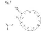
- the embodiment described above while the case has been described where chuck members 124 were placed almost on the entire surface of the lower surface of plate member 44 of chuck unit 153, the embodiment is not limited this, and for example, as is shown in FIG. 7 , in the embodiment described above only the chuck members 124 placed at the outer circumference section on the lower surface of plate member 44 whose suction force is adjusted by the second adjustment device 125b may be set. As a matter of course, in the case, the first adjustment device 125a is not necessary. Such a structure is suitable in a case when it is obvious that a desired flatness degree level of wafer W can be secured by only the chuck members 124 placed at the outer circumference section on the lower surface of plate member 44.
- wafer W can be made so that the desired level of flatness degree is secured by chuck members 124 and the three vertical-motion pins 140. In this case, for example, by adjusting the driving velocity of chuck unit driving system 144 and driving device 142 while monitoring the flatness degree of the wafer, it is possible to make wafer W have the desired level of flatness degree.
- the embodiment is not limited to this, and the suction force of the seven chuck members 124 can be weakened (reduced), or the suction force of a part of the chuck members 124 of the seven chuck members 124 can be weakened (or reduced to zero).
- the first adjustment device 125a may be structured so that the suction force of the plurality of (seven) chuck members 124 is adjustable individually, or in groups which are decided in advance.
- the second adjustment device 125b may be structured so that the suction force of the plurality of (eleven) chuck members 124 is adjustable individually, or in groups which are decided in advance.
- chuck unit 153 may wait in a state suctioning the wafer subject to the next exposure at the waiting position of the predetermined height above the loading position while exposure with respect to wafer W on wafer stage WST is being performed. In this case, wafer W can be controlled to a predetermined temperature even during the waiting.
- chuck unit 153 and the three vertical-motion pins 140 are driven downward synchronously (refer to FIGS. 6A and 6B ) while the suction state by chuck unit 153 (chuck member 124) and the support state by the three vertical-motion pins 140 with respect to wafer W are maintained.
- a driving force in the -Z direction by driving device 142 may act on the area adsorbed by the three vertical-motion pins 140 in the center of the lower surface of wafer W, which may cause the center section area of wafer W to deform (warp) in a downward protruded shape.
- a vertical-motion pin 240 related to a first modified example having a structure as is shown in a sectional view in FIG. 8 can be arranged on the upper surface of platform member 141.
- Vertical-motion pin 240 is equipped with an shaft member 70 fixed to the upper surface of platform member 141, and a suspended member 60 which is attached slidable in the vertical direction with respect to shaft member 70 and has a recess section 65 of a predetermined depth formed on a surface opposing platform member 141.
- Suspended member 60 is equipped with a support section 62, a slide section 64 and a stopper section 66.
- Support section 62 consists of a stepped rod-shaped member whose lower end is slightly thicker than other parts.
- Slide section 64 consists of a cylindrical (columnar) member which has a sectional shape when overlapping in a planar view the same with the lower end of support section 62.
- Slide section 64 has a recess section of a predetermined depth, for example, whose sectional shape is circular, formed in the lower end surface.
- Slide section 64 and support section 62 are integrated by fixing the lower end surface of support section 62 to the upper surface of slide section 64. Integration of slide section 64 and support section 62 is performed, for example, by bolting, by adhering or the like.
- an exhaust pipeline 68 is provided which runs from an exhaust opening 41 formed at the upper end surface of support section 62, passes through the inside of support section 62, furthermore passes through the inside of slide section 64, and opens at the outer circumference surface of slide section 64.
- an exhaust pipeline 68 is provided to the opening on the opposite side of exhaust opening 41 of exhaust pipeline 68 that has the other end connected to a vacuum pump which is not shown.
- Stopper section 66 consists of a ring-shaped member that has an outer circumferential surface substantially flush with the outer circumferential surface of slide section 64 and an inner circumferential surface that protrudes slightly inward than the inner circumferential surface of inner slide section 64, and on the inner circumferential side of its upper surface, a step section 67 is formed. Stopper section 66 and slide section 64 are integrated by stopper section 66 being fixed to the lower end surface of slide section 64. Integration of stopper section 66 and slide section 64 is performed, for example, by bolting, by adhering or the like. Incidentally, while support section 62, slide section 64, and stopper section 66 can be formed as separate members and then be integrated into suspended member 60, at least two parts can be integrally formed.
- Shaft member 70 consists of a stepped columnar member in which a part of the lower end has a diameter smaller than other parts.
- the outer diameter of of the large diameter section of shaft member 70 is slightly smaller than the inner diameter of the recess section of slide section 64, for example, by several ⁇ m to several tens of ⁇ m. Further, the outer diameter of the small diameter section of shaft member 70 is smaller by around several mms than the inner diameter of stopper section 66.
- the dimension in the height direction of shaft member 70 is a dimension in which the upper end surface of suspended member 60 is almost in contact with the bottom surface of the recess section of slide section 64, in a state where suspended member 60 is in contact with the platform member 141.
- a space 72 having a circular sectional shape of a predetermined depth is formed in the center section.
- a plurality of penetrating holes not shown that communicate with the outer circumferential surface from space are formed in a radial placement, at different height positions of the shaft member.
- a gas supply device for example, a compressor which is not shown is connected, via a gas supply pipeline and a gas supply pipe which are not shown.
- the supply amount or the like of gas (for example, compressed air) into space 72 by the gas supply device which is not shown is controlled by main controller 20.
- gas for example, compressed air
- the compressed air is made to blow out from between the outer circumferential surface of shaft member 70 and the inner circumferential surface of slide section 64, via a plurality of penetrating holes which are not shown formed in the side wall of shaft member 70. That is, an air static pressure bearing (air bearing) 76 is formed in between shaft member 70 and slide section 64.
- the outer circumferential surface of shaft member 70 (the inner circumferential surface of slide section 64) will be referred to as a guide surface 76, using the same reference sign as air bearing 76.
- a step section 74 is formed in the section at the border of the large diameter section and the small diameter section of shaft member 70, as is shown in FIG. 8 .
- Step section 67 of stopper section 66 is placed to face this step section 74.
- a predetermined gap (gap) exists in between the opposing surfaces of step section 74 and step section 67.
- suspended member 60 is drivable along guide surface 76 with respect to shaft member 70. Strokes in the vertical direction of suspended member 60 are restricted by stopper section 66. Meanwhile, movement of suspended member 60 in the horizontal plane is restricted (restrained) by shaft member 70.
- stopper section 66 since stopper section 66 only has to restrict the strokes in the vertical direction of suspended member 60, stopper section 66 does not necessarily have to be annular.
- wafer stage WST that has a wafer support section having three vertical-motion pins 240 with the structure described above provided on the upper surface of platform member 141
- loading of wafer W onto wafer table WTB is performed in a procedure similar to the embodiment described above.
- suspended member 60 of vertical-motion pin 240 is positioned at the lowest end position (movement lower limit position) within the stroke range.
- wafer W is driven downward along with chuck unit 153 and vertical-motion pins 240, while maintaining the predetermined gap with respect to chuck unit 153 (chuck member 124).
- vertical-motion pins 240 may be driven downward before chuck unit 153.
- shaft member 70 is driven along guide surface 76 downward with respect to slide section 64 within a range of predetermined strokes, in a state where the position of suspended member 60 is maintained.
- step section 74 of shaft member 70 hits step section 67 of stopper section 66, suspended member 60 will also be driven downward by driving device 142, along with shaft member 70.
- chuck unit 153 in case the responsiveness of chuck unit 153 is superior to the responsiveness of vertical-motion pins 240 and chuck unit 153 begins to move downward earlier on the synchronous drive, prior to starting the downward movement of chuck unit 153 immediately after wafer W suctioned in a non-contact manner by chuck unit 153 (chuck member 124) is supported from below by the three vertical-motion pins 240, shaft member 70 is positioned to the movement lower limit position where step section 74 hits the step section 67 of stopper section 66. This allows the generation of deformation (flexure) to an upward protruded shape of the center section of wafer W to be restrained.
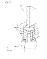
- Vertical-motion pin 340 related to a second modified example is basically structured in a similar manner as vertical-motion pin 240 previously described, however, the following points are different. That is, as is shown in FIG. 9 , vertical-motion pin 340 has an air chamber 71 and an exhaust hole 75 formed inside which are the points different from vertical-motion pin 240, and since other structures and functions are the same as in the first modified example, the description thereabout will be omitted.
- air chamber 71 is formed inside vertical-motion pin 340 (to be more precise, in between slide section 64 and shaft member 70). Air chamber 71 communicates with space 72, via an air flow passage 77 formed below. Therefore, a part of compressed air supplied into space 72 via a gas supply device which is not shown passes through air flow passage 77 and flows into air chamber 71. That is, the pressure in air chamber 71 is higher (positive pressure) when compared with the pressure in the space where vertical-motion pin 340 is placed, and a force in an upward direction is applied to suspended member 60.
- Exhaust hole 75 consists of an opening formed near the upper end of the side surface of slide section 64 (the side surface on the -X side in FIG. 9 ), and communicates with air chamber 71 via air flow passage 73. That is, a part of the compressed air flowing into air chamber 71 is constantly exhausted from exhaust hole 75.
- vertical-motion pin 340 serves as a damper due to viscous resistance of air such as when wafer W held by suction by wafer table WTB is separated from wafer table WTB by being pushed from below by vertical-motion pin 340, which can prevent wafer W from vibrating (jumping).
- vertical-motion pin 140 instead of vertical-motion pin 140, a vertical-motion pin 440 related to a third modified example below can be used.
- a vertical-motion pin 440 is equipped with a housing 86 fixed on the upper surface of platform member 141, and a shaft member 84 in which a part of the member is housed in housing 86.
- Housing 86 consists of a cylindrical member with a bottom that has an opening at the lower end surface and a space 85 formed inside. Further, in the upper wall (bottom section) of housing 86, a penetrating hole 87 having a circular sectional shape whose diameter is smaller than the inner diameter of housing 86 is formed in the vertical direction. In the inner circumferential surface section of penetrating hole 87 in the upper wall of housing 86, grooves which are not shown extending in the Z-axis direction are formed at an equal spacing in the radial direction in a planar view. Hereinafter, for the sake of convenience, the grooves will be described as groove 87, using the same reference sign as penetrating hole 87.
- Shaft member 84 consists of a columnar member whose diameter is slightly smaller than the diameter of penetrating hole 87 formed in the upper wall section of housing 86, and a flanged section 88 which projects outward is provided at the lower end. Flanged section 88 has an outer diameter larger than the inner diameter of penetrating hole 87. Shaft member 84 is inserted into penetrating hole 87 of housing 86 from below, and is allowed to move only in the Z-axis direction with respect to housing 86 within a predetermined stroke range. Shaft member 84 has a flanged section, a nut or the like which is not shown provided (or joined) at the outer circumference of the upper end so as to prevent the shaft member from dropping inside housing 86.
- the length of shaft member 84 in the long axis (Z-axis) direction can be increased with respect to housing 86, so that the upper surface of shaft member 84 is positioned above the upper surface of housing 86 when the shaft member 84 is positioned at the lowermost end of the strokes.
- a penetrating hole 83 is formed in the center section extending in the Z-axis direction, for example, having a circular sectional shape.
- Penetrating hole 83 has one end (the -Z end) connected to a vacuum pump which is not shown, via a piping which is not shown.
- wafer stage WST having a wafer support section in which three vertical-motion pins 440 of the structure described above are provided on the upper surface of platform member 141
- loading of wafer W onto wafer table WTB is performed in a procedure similar to the embodiment described above.
- shaft member 84 of vertical-motion pin 440 is at the lowest end position within the stroke range (or at a position in which the bottom surface is in contact with the upper surface of platform member 141).
- wafer W is driven downward with chuck unit 153 and vertical-motion pins 440, while a predetermined gap is maintained with respect to chuck unit 153 (chuck member 124).
- driving of vertical-motion pins 440 downward may start earlier than chuck unit 153, due to the difference of driving responsiveness between chuck unit 153 and vertical-motion pins 440.
- housing 86 is driven downward within the predetermined stroke range in a state where the position of shaft member 84 is maintained.
- an air flow occurs in groove 87, and in between shaft member 84 and housing 86, housing 86 is driven in a state where there is almost no friction (that is, a dynamic pressure bearing is structured in between shaft member 84 and housing 86).
- the embodiment is not limited to this, and for example, the dynamic pressure bearing can be structured by forming grooves on the outer circumferential surface of shaft member 84 in equal spacing in the axis direction.
- shaft member 84 and housing 86 can be a sliding bearing, using members having a small friction coefficient.
- the embodiments described above are not limited to this, and for example, can have a rectangular shape or the like, as long as wafer W can be suctioned from above in a non-contact manner.
- center support member 150 can be structured so that the three vertical-motion pins can vertically move independently, so as to keep the flatness degree of wafer W within a desired range by vertically moving the three vertical-motion pins individually, based on monitoring results of wafer flatness.
- the number of vertical-motion pins is not limited to three, and can be more or less than three pins.
- the embodiments described above can also be applied to an exposure apparatus in which a liquid immersion space including an optical path of an illumination light is formed between a projection optical system and a wafer and the wafer is exposed by the illumination light via the projection optical system and the liquid of the liquid immersion space, as is disclosed in, for example, PCT International Publication No.99/49504 , European Patent Application No. 1,420,298 , PCT International Publication No.2004/055803 , U.S. Patent No. 6,952,253 and the like. Further, the embodiments described above can also be applied to a liquid immersion exposure apparatus or the like disclosed in, for example, U.S. Patent Application Publication No.2008/0088843 .
- the embodiments described above are not limited to this, and the embodiments described above can also be applied to a stationary type exposure apparatus such as a stepper. Further, the embodiments described above can also be applied to a reduction projection exposure apparatus of the step-and-stitch method in which a shot area and a shot area are synthesized, an exposure apparatus of the proximity method, a mirror projection aligner or the like. Furthermore, the embodiments described above can also be applied to a multi-stage type exposure apparatus equipped with a plurality of wafer stages, as is disclosed in, for example, U.S. Patent No. 6,590,634 , U.S.
- Patent No. 5,969,441 U.S. Patent No. 6,208,407 or the like.
- the embodiments described above can also be applied to an exposure apparatus equipped with a measurement stage separate from the wafer stage, including a measurement member (for example, a reference mark, and/or a sensor or the like), as is disclosed in, for example, PCT International Publication No.2005/074014 or the like.
- the projection optical system in the exposure apparatus of the embodiments described above is not limited to a reduction system, and can either be an equal-magnifying or a magnifying system
- projection optical system PL is not limited to a refractive system, and can either be a reflection system or a catadioptric system, and its projection image can either be an inverted image or an erect image.
- the shape of the illumination area and the exposure area previously described was a rectangular shape, the embodiments are not limited to this, and for example, the shape can be an arc, a trapezoid, a parallelogram or the like.
- the light source of the exposure apparatus related to the embodiments described above is not limited to the ArF excimer laser, and a pulse laser light source such as a KrF excimer laser (output wavelength 248nm), an F 2 laser (output wavelength 157nm), an Ar 2 laser (output wavelength 126nm), or a Kr 2 laser (output wavelength 146nm), a super high pressure mercury lamp which generates a bright line such as a g-line (wavelength 436nm), an i-line (wavelength 365nm), or the like can also be used. Further, a harmonic wave generating device which uses a YAG laser can also be used. As other light sources, as is disclosed in, for example, U.S. Patent No.
- a harmonic wave can also be used as vacuum ultraviolet light, in which a single-wavelength laser beam in the infrared range or the visible range emitted by a DFB semiconductor laser or a fiber laser is amplified by a fiber amplifier doped with, for example, erbium (or both erbium and ytterbium) and wavelength conversion into ultraviolet light is performed using a nonlinear optical crystal.
- the light is not limited to light having a wavelength of 100nm or more, and as a matter of course, light having a wavelength less than 100nm can also be used.
- the embodiments described above can suitably be applied to an EUV exposure apparatus which uses EUV (Extreme Ultraviolet) light in the soft X-ray region (for example, a wavelength region of 5 to 15nm).
- EUV Extreme Ultraviolet
- the embodiments described above can also be applied to an exposure apparatus which uses a charged particle beam such as an electron beam or an ion beam.
- the embodiments described above can also be applied to an exposure apparatus which synthesizes two reticle patterns on a wafer via the projection optical system and performs double exposure almost simultaneously on a shot area on the wafer by performing scanning exposure once, as is disclosed in, for example, U.S. Patent No. 6,611,316 .
- the obj ect on which the pattern should be formed is not limited to the wafer, and may be other objects such as a glass plate, a ceramic substrate, a film member, or a mask blank.
- the usage of the exposure apparatus is not limited to the exposure apparatus for manufacturing semiconductors, and the embodiments above can be widely applied, for example, to an exposure apparatus for liquid crystals that transfers a liquid crystal display devices pattern onto a square-shaped glass plate, an exposure apparatus for manufacturing an organic EL, a thin film magnetic head, an imaging element (such as a CCD), a micromachine and a DNA chip or the like. Further, the embodiments described above can also be applied to an exposure apparatus that transfers a circuit pattern onto a glass substrate or a silicon wafer for manufacturing a reticle or a mask that is used in not only microdevices such as semiconductor devices, but also used in an optical exposure apparatus, an EUV exposure apparatus, an X-ray exposure apparatus, an electron beam exposure apparatus or the like.
- Electronic devices such as semiconductor devices are manufactured through the steps such as; a step for performing function/performance design of a device, a step for making a reticle based on this design step, a step for making a wafer from a silicon material, a lithography step for transferring a pattern of a mask (reticle) onto the wafer by the exposure apparatus (pattern generating device) and the exposure method related to the embodiments described above, a development step for developing the wafer which has been exposed, an etching step for removing by the etching an exposed member of an area other than the area where the resist remains, a resist removing step for removing the resist that is no longer necessary since etching has been completed, a device assembly step (including a dicing process, a bonding process, and a package process), and an inspection step.
- a highly integrated device can be manufactured with good productivity
Abstract
Description
- The present invention relates to suction devices, carry-in methods, carrier systems and exposure apparatuses, and device manufacturing methods, and more particularly to a suction device in which its suction force acts in a non-contact manner on a plate-like object, a carry-in method in which carry-in is performed of the plate-like object onto a movable body, a carrier system suitable for carrying out the carry-in method and an exposure apparatus which is equipped with the carrier system, and a device manufacturing method which uses the exposure apparatus.
- Conventionally, in a lithography process to manufacture electronic devices (microdevices) such as a semiconductor device (an integrated circuit or the like) or a liquid crystal display device, mainly, a projection exposure apparatus of a step-and-repeat method (a so-called stepper), projection exposure apparatus of a step-and-scan method (a so-called scanning stepper (also called a scanner)) or the like is mainly used.
- Substrates such as a wafer, a glass plate and the like subject to exposure that are used in these types of exposure apparatuses are gradually becoming larger (for example, in the case of a wafer, in every ten years). Although a 300-mm wafer which has a diameter of 300mm is currently the mainstream, the coming of age of a 450mm wafer which has a diameter of 450mm looms near. When the transition to 450mm wafers occurs, the number of dies (chips) output from a single wafer becomes double or more than the number of chips from the current 300mm wafer, which contributes to reducing the cost.
- However, because the thickness does not necessarily increase in proportion to the size of the wafer, the 450mm wafer is extremely weak in intensity and rigidity when compared with the 300mm wafer. Therefore, when focusing on a point such as a carriage of a wafer, it was considered that there was a risk of warping occurring in the wafer, which may negatively effect the exposure accuracy when a means method similar to the current 300mm wafer was employed. Accordingly, as the carry-in method of the wafer, a proposal is made of a carry-in method or the like that can be employed even when the wafer is a 450mm wafer in which the wafer is suctioned from above in a non-contact manner by a carrier member equipped with a Bernoulli chuck or the like to maintain the flatness degree (flatness) and performs carry-in onto a wafer holder (holding device) (for example, refer to PTL 1).
- However, in the case of employing the non-contact suction from above by the carrier member described above as a carry-in method of the wafer onto the wafer stage (wafer holder), there was a risk of positional deviation (rotation deviation) in a horizontal plane of the wafer being generated at an unacceptable level, to which correction based on measurement results was difficult to perform.
-
- As a method for resolving the inconvenience due to suction in a non-contact manner from above by the wafer carrier member described above, a method can be considered in which while a wafer is suctioned in a non-contact manner suction from above by a Bernoulli chuck or the like, the wafer is also supported from below by a support section (for example, vertical-motion pins on a wafer stage). However, according to studies of the inventors, in the case of performing loading of the wafer onto the wafer stage in a non-contact suction from above the wafer and support from below, it became clear that warping that is not acceptable could occur even in the case of a 300mm wafer. By investigating the cause of this warping of the wafer, the inventors reached a conclusion that the main factor is surplus-restraint which occurs due to the wafer being vertically restrained around the center of the wafer.
- According to a first aspect of the present invention, there is provided a first suction device in which a suction force is made to act on a plate-like object in a non-contact manner, comprising: a base member; and a plurality of suction members provided at the base member that each generates a gas flow around the obj ect to make a force which suctions the obj ect, wherein the plurality of suction members generate the gas flow in a mutually different state.
- According to this device, the suction force with respect to the object generated by each of the plurality of suction members, can be made different according to, for example, the position on the base member of each suction member. Therefore, for example, in the case of performing support of the object from below by the support section and suction in a non-contact manner from above of the object by this suction device, it becomes possible to make the suction force generated by the suction members placed at a part facing the support section of the base member be weaker than the suction force generated by the suction members placed at a part which does not face the support section of the base member.
- According to a second aspect of the present invention, there is provided a second suction device in which a suction force is made to act on a plate-like object in a non-contact manner, comprising: a base member; a plurality of gas flow holes provided at the base member that each generates a gas flow around the object; and an adjustment device which deforms the object, wherein the object is deformed by the adjustment device while the object is held by the gas flow via the plurality of gas flow holes.
- According to this device, while holding the object by the gas flow via the plurality of gas flow holes, it becomes possible for the adjustment device to deform the object, for example, so that a desired level of flatness is secured.
- According to a third aspect of the present invention, there is provided a carry-in method in which carry-in of a plate-like object onto a holding member having an object mounting surface provided on its upper surface is performed, the method comprising: carrying the object above the object mounting surface of the holding member at a predetermined carry-in position; suctioning a surface of the object from above by a suction member in a non-contact manner; supporting from below a part of a center section area at an other surface on an opposite side of the surface of the object suctioned by the suction member by a vertically movable support section provided at the holding member, and weakening a suction force by the suction member with respect to an area of the surface of the object corresponding to the center section area including a supporting point by the support section; and driving the suction member and the support section downward toward the object mounting surface, in a state maintaining a suction state by the suction member and a support state by the support section with respect to the object.
- According to this method, it becomes possible to perform carry-in of the object onto the holding member in a state where the flatness degree of the object is highly maintained.
- According to a fourth aspect of the present invention, there is provided a carrier system in which a plate-like object is carried, comprising: a holding member in which an object mounting surface is provided at its upper surface; a vertically movable suction member provided above the holding member at a predetermined carry-in position, the suction member being able to suction a plurality of places including at least an area at an outer circumference section of a surface of the object from above in a non-contact manner; a support section provided at the holding member, the support section being vertically movable and can support from below a part of the center section area at an other surface on an opposite side of the surface of the object; and a driving device which drives the suction member and the support section downward so that the other surface of the object moves toward the object mounting surface of the holding member, in a state where a suction state by the suction member and a support state by the support section with respect to the object is maintained.
- According to this system, it becomes possible to perform carrier (carry-in) of the object onto the holding member in a state where the flatness degree of the object is highly maintained.
- According to a fifth aspect of the present invention, there is provided a first exposure apparatus which forms a pattern on an object, comprising: the suction device related to any of the first and second aspects described above; and a pattern generating device in which the pattern is formed by exposing the object suctioned by the suction device and carried in on the holding member with an energy beam.
- According to a sixth aspect of the present invention, there is provided a second exposure apparatus which forms a pattern on an object, comprising: the carrier system described above; and a pattern generating device in which the pattern is formed by exposing the object carried in on the holding member by the carrier system with an energy beam.
- According to a seventh aspect of the present invention, there is provided a device manufacturing method, including: exposing an object using the exposure apparatus described above; and developing the object which has been exposed.
-
-
FIG. 1 is a view schematically showing a structure of an exposure apparatus related to an embodiment. -
FIG. 2 is a view (front view) of a wafer stage inFIG. 1 when viewed from a -Y direction. -
FIG. 3A is a bottom surface view which shows a carry-in unit (chuck unit) inFIG. 1 , andFIG. 3B is a view showing each part related to loading of a wafer and shows the carry-in unit, along with vertical-motion pins on the wafer stage and its driving device. -
FIG. 4 is a block diagram showing an input/output relation of a main controller which mainly structures a control system of the exposure apparatus related to the embodiment. -
FIGS. 5A to 5D are views (No. 1 to No. 4) used for explaining a carry-in procedure of the wafer. -
FIGS. 6A to 6c are views (No. 5 to No. 7) used for explaining the carry-in procedure of the wafer. -
FIG. 7 is a view used for explaining another example of an arrangement of chuck members provided in the chuck unit. -
FIG. 8 is a view showing a structure of a vertical-motion pin related to a first modified example. -
FIG. 9 is a view showing a structure of a vertical-motion pin related to a second modified example. -
FIG. 10 is a view showing a structure of a vertical-motion pin related to a third modified example. - An embodiment will be described below, based on
FIGS. 1 to 7 . -
FIG. 1 schematically shows a structure of anexposure apparatus 100 related to an embodiment. Thisexposure apparatus 100 is a projection exposure apparatus of a step-and-scan method, or a so-called scanner. As it will be described later on, a projection optical system PL is arranged in the present embodiment, and in the description below, a direction parallel to an optical axis AX of this projection optical system PL will be described as a Z-axis direction, a direction within a plane orthogonal to the Z-axis direction in which a reticle R and a wafer W are relatively scanned will be described as the Y-axis direction, a direction orthogonal to the Z-axis and the Y-axis will be described as an X-axis direction, and rotational (inclination) direction around the X-axis, the Y-axis, and the Z-axis will be described as a θx direction, a θy direction, and a θz direction. -
Exposure apparatus 100 is equipped with anillumination system 10, a reticle stage RST which holds reticle (mask) R, projection optical system PL, a wafer stage WST which holds wafer W, a carry-inunit 121 which structures a wafer carrier system 120 (refer toFIG. 4 ) along with a carry-out unit which is not shown and a vertical-motion pin which will be described later on, and a control system or the like of these parts. -
Illumination system 10, as is disclosed in, for example,U.S. Patent Application Publication No. 2003/0025890 and the like, includes a light source, an illuminance equalizing optical system including an optical integrator and the like, and an illumination optical system that has a reticle blind and the like (none of which are shown) .Illumination system 10 illuminates a slit-shaped illumination area IAR set (limited) on reticle R by the reticle blind (also called a masking system) by an illumination light (exposure light) IL, with a substantially uniform illuminance. In this case, as illumination light IL, for example, an ArF excimer laser beam (wavelength 193nm) is used. - On reticle stage RST, reticle R on which a circuit pattern or the like is formed on its pattern surface (the lower surface in
FIG. 1 ) is fixed, for example, by vacuum chucking. Reticle stage RST, for example, is finely drivable within the XY plane by a reticle stage driving system 11 (not shown inFIG. 1 , refer toFIG. 4 ) including a linear motor, a planar motor or the like, and is also drivable in a scanning direction (the Y-axis direction which is the lateral direction of the page surface inFIG. 1 ) at a predetermined scanning speed. - Position information (including rotation information in the θz direction) of reticle stage RST in the XY plane is constantly detected, for example, by a reticle laser interferometer (hereinafter, referred to as a "reticle interferometer") 13, via a movable mirror 15 (actually, a Y movable mirror (or a retroreflector) having a reflection surface orthogonal to the Y-axis direction and an X movable mirror having a reflection surface orthogonal to the X-axis direction are provided) fixed to reticle stage RST, at a resolution of, for example, around 0.25nm. Measurement values of
reticle interferometer 13 are sent to a main controller 20 (not shown inFIG. 1 , refer toFIG. 4 ).Main controller 20 drives reticle stage RST via reticle stage driving system 11 (refer toFIG. 4 ), based on the position information of reticle stage RST. Incidentally, in the present embodiment, position information of reticle stage RST in the XY plane can be detected using an encoder, instead of the reticle interferometer described above. - Projection optical system PL is placed below reticle stage RST in
FIG. 1 . Projection optical system PL is mounted on a main frame BD supported horizontally by a support member which is not shown. Used as projection optical system PL, for example, is a dioptric system consisting of a plurality of optical elements (lens elements) arranged along optical axis AX, which is parallel to the Z-axis. Projection optical system PL, for example, is double telecentric, and has a predetermined projection magnification (for example, 1/4 times, 1/5 times or 1/8 times). Therefore, when illumination area IAR on reticle R is illuminated by illumination light IL fromillumination system 10, a reduced image of the circuit pattern of reticle R (a reduced image of a part of the circuit pattern) within illumination area IAR is formed in an area (hereinafter, also called an exposure area) IA conjugate to illumination area IAR on wafer W whose surface is coated with a resist (sensitive agent) and is placed on a second surface (image plane) side of projection optical system PL, via projection optical system PL, by illumination light IL having passed through reticle R placed so that its pattern surface substantially coincides with a first surface (object plane) of projection optical system PL. And, by reticle stage RST and wafer stage WST (to be more precise, fine movement stage WFS to be described later on which holds wafer W) being synchronously driven, scanning exposure of a shot area (divided area) on wafer W is performed, by reticle R being relatively moved in the scanning direction (Y-axis direction) with respect to illumination area IAR (illumination light IL) and wafer W being relatively moved in the scanning direction (Y-axis direction) with respect to exposure area IA (illumination light IL), and the pattern of reticle R is transferred onto the shot area. That is, in the present embodiment, the pattern of reticle R is generated on wafer W byillumination system 10 and projection optical system PL, and by the exposure of the sensitive layer (resist layer) on wafer W with illumination light IL the pattern is formed on wafer W. - Wafer stage WST, as is shown in
FIG. 1 , is supported by levitation onbase board 12, via air bearings which will be described later on. Here,base board 12 is supported almost horizontally (parallel to the XY plane) on a floor F by a vibration-proof mechanism (omitted in drawings).Base board 12 consists of a member that has a flat plate-like outer shape. Further, insidebase board 12, a coil unit is housed, which includes a plurality ofcoils 17 placed in the shape of a matrix with the XY two-dimensional direction serving as a row direction and a column direction. - Wafer stage WST, as it can be seen from
FIGS. 1 and2 , has a coarse movement stage WCS, and a fine movement stage WFS, which is supported in a non-contact state by coarse movement stage and is relatively movable with respect to coarse movement stage WCS. Here, wafer stage WST (coarse movement stage WCS) is driven in predetermined strokes in the X-axis direction and the Y-axis direction, and is also finely driven in the θz direction by a coarse movement stage driving system 51 (refer toFIG. 4 ). Further, fine movement stage WFS is driven in directions of six degrees of freedom (the X-axis direction, the Y-axis direction, the Z-axis direction, the θx direction, the θy direction and the θz direction) by a fine movement stage driving system 52 (refer toFIG. 4 ), with respect to coarse movement stage WCS. - Coarse movement stage WCS, as is shown in
FIG. 2 , is equipped with a coarsemovement slider section 91 having a rectangular plate-like shape whose length in the X-axis direction is slightly longer than the length in the Y-axis direction in a planar view (when viewed from the +Z direction), a pair ofside wall sections movement slider section 91 in the longitudinal direction in a state parallel to the YZ plane, and a pair ofstator sections side wall sections side wall sections stator sections side wall sections movement slider section 91, at one end and the other end in the longitudinal direction. - At the bottom surface of coarse movement stage WCS, that is, at the bottom surface of coarse
movement slider section 91, a magnet unit corresponding to the coil unit placed insidebase board 12 is provided, consisting of a plurality ofpermanent magnets 18 placed in the shape of a matrix with the XY two-dimensional directions serving as a row direction and the column direction. The magnet unit, along with the coil unit ofbase board 12, structures coarse movement stage driving system 51 (refer toFIG. 4 ) consisting of a planar motor of an electromagnetic force (Lorentz force) driving method whose details are disclosed, for example, inU.S. Patent No. 5,196,745 and the like. The magnitude and direction of the electric current supplied to eachcoil 17 structuring the coil unit (refer toFIG. 1 ) are controlled bymain controller 20. - At the bottom surface of coarse
movement slider section 91, a plurality ofair bearings 94 is fixed around the magnet unit described above. Coarse movement stage WCS is supported by levitation by the plurality ofair bearings 94, via a predetermined gap (clearance, gap) abovebase board 12, such as for example, a gap of about several µm, and is driven in the X-axis direction, the Y-axis direction and the θz direction by coarse movementstage driving system 51. - Incidentally, coarse movement
stage driving system 51 is not limited to the planar motor of the electromagnetic force (Lorentz force) driving method, and for example, a planar motor of a variable magneto-resistance driving method can also be used. Other than this, coarse movementstage driving system 51 can be structured by a magnetic levitation type planar motor, and the planar motor can driving coarse movement stage WCS in directions of six degrees of freedom. In this case, the air bearings will not have to be arranged at the bottom surface of coarsemovement slider section 91. - Each of the pair of
stator sections main controller 20. - Fine movement stage WFS, as is shown in
FIG. 2 , for example, is equipped with amain section 81 consisting of a low-height columnar member having an octagonal shape in a planar view, a pair ofmover sections main section 81, and a wafer table WTB consisting of a rectangular plate-shaped member when viewed from above, which is integrally fixed to the upper surface ofmain section 81. -
Main section 81 is preferably made of a material having a thermal expansion coefficient is the same or around the same level as that of wafer table WTB, and the material is preferably a material having a low thermal expansion coefficient. Here, although it is omitted in the drawing inFIG. 2 , atmain section 81, a plurality of (for example, three) vertical-motion pins 140 (refer toFIG. 3B ) being vertically movable is provided, which are inserted into through holes which are not shown formed in wafer table WTB (and in a wafer holder which is not shown). At the upper surface of each of the three vertical-motion pins 140, anexhaust opening 41 is formed for vacuum exhaust. Further, each of the three vertical-motion pins 140 has the lower end surface fixed to the upper surface of aplatform member 141. Each of the three vertical-motion pins 140 is placed at a position which is almost the vertex of an equilateral triangle in a planar view on the upper surface ofplatform member 141.Exhaust opening 41 provided at each of the three vertical-motion pins 140 is connected to a vacuum pump (not shown), via an exhaust pipeline formed inside vertical-motion pin 140 (and platform member 141) and a vacuum exhaust piping which is not shown.Platform member 141 is connected to adriving device 142, via ashaft 143 fixed at the center of the lower surface. That is, the three vertical-motion pins 140 are driven in the vertical direction by drivingdevice 142, integrally withplatform member 141. In the present embodiment,platform member 141, the three vertical-motion pins 140 andshaft 143 structure awafer support section 150, which can support from below a part of a center section area of the wafer lower surface. Here, displacement in the Z-axis direction from a reference position of the three vertical-motion pins 140 (wafer support section 150) is detected by a displacement sensor 145 (not shown inFIG. 3B , refer toFIG. 4 ), such as, for example, the encoder system provided at drivingdevice 142.Main controller 20, based on measurement values ofdisplacement sensor 145, drives the three vertical-motion pins 140 (wafer support section 150) in the vertical direction via drivingdevice 142. - Referring back to
FIG. 2 , each of the pair ofmover sections main section 81. Hereinafter, for the sake of convenience, the housings will be described ashousings mover sections -
Housing 82a has a hollow section whose YZ section is a rectangular shape elongate in the Y-axis direction, with the Y-axis direction dimension (length) and the Z-axis direction dimension (height) both slightly longer thanstator section 93a. In the hollow section ofhousings stator section 93a of coarse movement stage WCS is inserted in a non-contact manner. Inside anupper wall section 82a1 and abottom wall section 82a2 ofhousing 82a, magnet units MUa1, MUa2 are provided. -
Mover section 82b is structured in a similar manner, although the structure is symmetrical tomover section 82a. In the hollow section of housing (mover section) 82b, the end on the +X side ofstator section 93b of coarse movement stage WCS is inserted in a non-contact manner. Inside anupper wall section 82b1 andbottom wall section 82b2 ofhousing 82b, magnet units MUb1, MUb2 are provided, which are structured similarly to magnet units MUa1, MUa2. - Coil units CUa, CUb described above are housed, respectively, inside
stator sections - The structure of magnet units MUa1, MUa2 and magnet units MUb1, MUb2, and coil units CUa, CUb, is disclosed in detail, for example, in
U.S. Patent Application Publication No.2010/0073652 ,U.S. Patent Application Publication No.2010/0073653 and the like. - In the present embodiment, fine movement stage driving system 52 (refer to
FIG. 4 ) in which fine movement stage WFS is supported by levitation in a non-contact state with respect to coarse movement stage WCS and is also driven in a non-contact manner in directions of six degrees of freedom is structured similarly to theU.S. Patent Application Publication No. 2010/0073652 and theU.S. Patent Application Publication No. 2010/0073653 described above, including the pair of magnet units MUa1, MUa2 thatmover section 82a previously described has and coil unit CUa thatstator section 93a has, and the pair of magnet units MUb1, MUb2 thatmover section 82b has and coil unit CUb thatstator section 93b has. - Incidentally, in the case of using a magnetic levitation type planar motor as coarse movement stage driving system 51 (refer to
FIG. 4 ), because fine movement stage WFS can be finely driven in the Z-axis direction, the θx direction and the θy direction integrally with coarse movement stage WCS by the planar motor, fine movementstage driving system 52 can be structured so that fine movement stage WFS is drivable in the X-axis direction, the Y-axis direction and the θz direction, or that is, in directions of three degrees of freedom in the XY plane. Other than this, for example, to each of the pair ofside wall sections mover sections stator sections - In the center on the upper surface of wafer table, wafer W is fixed by vacuum chucking or the like via the wafer holder which is not shown such as a pin chuck. Further, on wafer table WTB, a movable mirror 27 (illustrated as
movable mirrors FIG. 2 ) which reflects the laser beam from a wafer laser interferometer (hereinafter referred to as a "wafer interferometer") 31 (refer toFIG. 1 ) is fixed, and bywafer interferometer 31 fixed to main frame BD in a suspended state, position of wafer table WTB in the XY plane is constantly detected, for example, at a resolution of around 0.25 to 1nm. Here, actually, as is shown inFIG.2 , on wafer table WTB,movable mirror 27Y having a reflection surface orthogonal to the Y-axis direction which is the scanning direction andmovable mirror 27X having a reflection surface orthogonal to the X-axis direction which is the non-scanning direction are provided, andwafer interferometer 31 is provided with one axis in the scanning direction and two axes in the non-scanning direction, however, inFIG. 1 , these are representatively shown asmovable mirror 27 andwafer interferometer 31. Position information (or velocity information) of wafer table WTB is sent tomain controller 20.Main controller 20 controls the movement of wafer table WTB in the XY plane, via coarse movementstage driving system 51 and fine movementstage driving system 52, based on the position information (or velocity information). Incidentally, the position information of wafer table WTB in the XY plane can be detected using, for example, an encoder system in which a scale (diffractive grating) or a head is mounted on wafer table WTB, instead ofwafer interferometer 31. Further, in the present embodiment, while wafer stage WST was a coarse fine movement stage equipped with coarse movement stage WCS and fine movement stage WFS, the present invention is not limited to this, and the wafer stage may be structured by a single stage which is movable in directions of six degrees of freedom. - Carry-in
unit 121 is a unit for holding the wafer before exposure above the loading position prior to loading the wafer onto wafer table WTB and loading the wafer onto wafer table WTB. Further, the carry-out unit which is not shown is a unit for unloading the wafer after exposure from wafer table WTB. - Carry-in
unit 121, as is shown inFIG. 1 , is equipped with a chuckunit driving system 144 attached to main frame BD via ananti-vibration device 42, achuck unit 153 and the like.Anti-vibration device 42 is a device for suppressing or preventing vibration generated at the time of drivingchuck unit 153 by chuckunit driving system 144 from travelling to main frame BD, that is, for vibrationally separatingchuck unit 153 from main frame BD. Accordingly, chuckunit driving system 144 andchuck unit 153 can be provided at another member, which is physically separate from main frame BD. -
Chuck unit 153, as is shown inFIG. 3B , for example, is equipped with aplate member 44 of a predetermined thickness having a circular shape in a planar view, and a plurality ofchuck members 124 fixed in a predetermined placement to the lower surface ofplate member 44. Here,plate member 44 may also function as a cool plate in which piping and the like are provided inside, and by liquid controlled to a predetermined temperature flowing in the piping, the wafer is controlled to a predetermined temperature. - In the present embodiment, as is shown in
FIG. 3a which is a planar view ofchuck unit 153 when viewed from the -Z direction, at the lower surface ofplate member 44 lower surface, sevenchuck members 124 are placed at the center section area including the center point and at the outer periphery in a stat surrounding these sevenchuck members 124 , elevenchuck members 124 are placed. The sixchuck members 124 that surroundchuck member 124 positioned at the center point of the lower surface ofplate member 44, are provided at positions substantially facing vertical-motion pins 140 when wafer stage WST is positioned at the loading position. - Each
chuck member 124 consists of a so-called Bernoulli chuck. Bernoulli chuck, as is well known, is a chuck which uses the Bernoulli effect so that the flow velocity of the fluid blowing out (for example, air) is locally increased to suction (hold in a non-contact manner) the target object. Here, Bernoulli effect is an effect in which the pressure of the fluid decreases when the flow velocity increases, and with the Bernoulli chuck, the suction state (hold/levitation state) is determined by the weight of the target object to be suctioned (held, fixed), and the flow amount (flow velocity, pressure) of the fluid blown out from the chuck. That is, in the case the size of the target object is known, the size of the gap between the chuck and the target object to be held is determined according to the flow amount (flow velocity) of the fluid blown out from the chuck. In the present embodiment,chuck member 124 is used to suction wafer W, by blowing out gas from its gas flow holes (for example, a nozzle or a blowout port) and generating a flow of gas (gas flow) in the periphery of wafer W (refer toFIG. 3B ). The degree of the force of suction (that is, the flow velocity and the like of the gas blown out) can be appropriately adjusted, and by suctioning wafer W withchuck member 124 and performing suction hold of the wafer, movement in the Z-axis direction, the θx direction and the θy direction can be restricted. - Further, with the plurality of
chuck members 124, flow velocity of the gas and the like blown out from each member is controlled bymain controller 20, via afirst adjustment device 125a or asecond adjustment device 125b (refer toFIG. 4 ). This allows the suction force (adsorption force) of eachchuck member 124 to be set to any value. In the present embodiment, the suction force of eachchuck member 124 is controlled, via thefirst adjustment device 125a or thesecond adjustment device 125b (refer toFIG. 4 ) in groups. Thefirst adjustment device 125a has a first fluid supply device which is not shown connected to the sevenchuck members 124 placed at the center section area of theplate member 44 lower surface, and adjusts the suction force of the seven chuck members 124 (adjusts the flow velocity of the fluid (gas, for example, air) blown out from chuck member 124). Further, thesecond adjustment device 125b has a second fluid supply device which is not shown connected to the elevenchuck members 124 placed in the area excluding the center section area (that is, the outer circumference section) of theplate member 44 lower surface, and adjusts the suction force of the elevenchuck members 124. That is, in the present embodiment, agas supply device 50 including thefirst adjustment device 125a and thesecond adjustment device 125b is structured, which supplies fluid (gas, for example, air) to the plurality of (in this case, 18)chuck members 124. -
FIG. 3A showschuck members 124 whose suction force is adjusted by thefirst adjustment device 125a and chuckmembers 124 whose suction force is adjusted by thesecond adjustment device 125b, classified by color. Incidentally, in the present embodiment, while the suction force of each chuck member is made adjustable by performing blowout of the fluid (gas) at a different flow velocity as a state different from each other in the plurality of chuck members, the embodiment is not limited to this. For example, the pressure of the fluid (gas) may be changed, or the flow amount may be changed. Further, a structure may also be employed in which the plurality ofchuck members 124 are not grouped and the suction forces can be individually adjusted. -
Chuck unit 153 is drivable in predetermined strokes in the Z-axis direction (in between a first position where wafer W carried in by a carrier arm 149 (refer toFIG. 5A ) which is described later is suctioned and a second position where the suctioned wafer W is mounted on wafer table WTB), by chuck unit driving system 144 (refer toFIG. 3B ). Chuckunit driving system 144 is controlled by main controller 20 (refer toFIG. 4 ). - Referring back to
FIG. 1 , on the -Y side of projection optical system PL, an off-axisalignment detection system 99 is provided. Asalignment detection system 99, for example, an FIA (Field Image Alignment) system alignment sensor of an image processing method is used, which irradiates a broadband detection beam that is not sensitive to the resist on wafer W on the subject mark, picks up an image of the subject mark formed on the light-receiving plane by the reflected light from the subject mark and an index image not shown using an imaging element (CCD) or the like, and outputs the imaging signals. The imaging results of thisalignment detection system 99 are sent tomain controller 20. - Although it is not shown in
FIG. 1 , above reticle R, a pair of reticle alignment detection systems 14 (refer toFIG. 4 ) of a TTR (Through The Reticle) method is placed that uses an exposure wavelength to simultaneously observe a pair of reticle alignment marks on reticle R and an image via projection optical system PL of a pair of first reference marks on a reference mark plate which is not shown on wafer table WTB corresponding to the reticle alignment marks. Detection signals of the pair of reticlealignment detection systems 14 are supplied tomain controller 20. - Other than this, in
exposure apparatus 100, a multi-point focal point detection system 54 (refer toFIG. 4 ) is provided, consisting of an irradiation system and a light-receiving system which are placed withalignment detection system 99 in between, and being structured in a similar manner as the system disclosed in, for example,U.S. Patent No.5, 448, 332 and the like. -
FIG. 4 shows a block diagram illustrating an input/output relation of controlmain controller 20, which mainly structures the control system ofexposure apparatus 100 and has overall control over each section.Main controller 20 includes a work station (or a microcomputer) or the like, and has overall control over each section ofexposure apparatus 100. - In
exposure apparatus 100 related to the present embodiment structured in the manner described above, first of all, reticle loading is performed by a reticle loader under the control ofmain controller 20. Next, bymain controller 20, preparatory operations such as base line measurement ofalignment detection system 99 are performed according to a predetermined procedure, using the pair of reticle alignment detection systems 14 (refer toFIG. 4 ), the reference mark plate (not shown) on wafer stage WST, and alignment detection system 99 (refer toFIGS.1 and4 ) and the like. Loading of the wafer is performed after these preparatory operations. - Now, the procedure of loading of wafer W will be described based on
FIGS. 5A to 6C . As a premise, chuckunit driving system 144 is to be driven bymain controller 20, andchuck unit 153 is to be moved to a position (waiting position) at a predetermined height within the stroke range and to be waiting at this position. - In this state, first of all, as is shown in
FIG. 5A ,carrier arm 149 holding wafer W under the control ofmain controller 20 is moved to a position underchuck unit 153. That is, wafer W is carried to a position belowchuck unit 153 bycarrier arm 149. Next, as is shown by the outlined arrow inFIG. 5A ,carrier arm 149 holding wafer W moves upward by a predetermined amount. On this operation, a high-pressure air flow is made to blow out from all thechuck members 124 ofchuck unit 153, via each gas flow hole. - Then, when
carrier arm 149 is moved upward by a predetermined amount, as is shown inFIG. 5B , the upper surface of wafer W is suctioned in a non-contact manner by all thechuck members 124 ofchuck unit 153. Next,main controller 20 withdrawscarrier arm 149 from under wafer W, after separatingcarrier arm 149 and wafer W. By this operation, wafer W moves to a state suctioned in a non-contact manner bychuck unit 153 located at a predetermined height position (waiting position) at the loading position. On this operation, while wafer W is in a state held bychuck unit 153 where its movement is restricted in the Z-axis direction, the θx direction, and the θy direction by the suction ofchuck unit 153, another member for holding wafer W may be prepared so thatchuck unit 153 provides only the suction force (a force which can perform suction but not holding) to wafer W. - In this state,
main controller 20 drives wafer stage WST via coarse movement stage driving system 51 (refer toFIG. 4 ) to t position under wafer W held bychuck unit 153.FIG. 5B shows wafer table WTB in the state after this movement of wafer stage WST. - Next,
main controller 20, as is shown inFIG. 5C , drives the three vertical-motion pins 140 (wafer support section 150) on wafer stage WST (refer toFIG. 3B ) upward, via drivingdevice 142. Then, when the three vertical-motion pins 140 come into contact with the lower surface of wafer W suctioned bychuck unit 153,main controller 20 stops the upward drive ofwafer support section 150. Here, the Z position of wafer W suctioned bychuck unit 153 located at the waiting position can be obtained accurately to some extent. Accordingly, by drivingwafer support section 150 by a predetermined amount from the reference position based on the measurement results ofdisplacement sensor 145,main controller 20 can make the three vertical-motion pins 140 come into contact with the lower surface of wafer W suctioned bychuck unit 153. However, the arrangement is not limited to this, and it can be set in advance so that the three vertical-motion pins 140 come into contact with the lower surface of wafer W suctioned bychuck unit 153 at the upper limit of the movement position of wafer support section 150 (the three vertical-motion pins 140). - Then,
main controller 20 operates a vacuum pump which is not shown, and begins the vacuum chucking with respect to the wafer W lower surface by the three vertical-motion pins 140. Incidentally, suction (holding) of wafer W bychuck member 124 is still being continued in this state. Movement of wafer W is restricted by the suction bychuck member 124 and a frictional force by the support from below of vertical-motion pins 140, in directions of six degrees of freedom. - When wafer W is supported (suction hold is performed) by the three vertical-
motion pins 140, as is shown inFIG. 5D ,main controller 20 releases the suction of wafer W by the sevenchuck members 124 by stopping the outflow of the high-pressure air flow from the sevenchuck members 124 at the center section area, via thefirst adjustment device 125a (refer toFIG. 4 ). This is because when suction hold (support) by the three vertical-motion pins 140 from below and suction bychuck unit 153 from above is performed with respect to wafer W as is shown inFIG. 5C , partial surplus-restraint may occur in wafer W. When a downward synchronous drive ofchuck unit 153 and wafer support section 150 (the three vertical-motion pins 140) to load wafer W onto wafer table WTB is performed in the manner described below in this partially surplus state, in the case the chuck unit and the wafer support section lose synchronization, warping may occur in wafer W. Therefore, to prevent such a situation from occurring, the suction of wafer W by the sevenchuck members 124 was released. - Next,
main controller 20, as is shown inFIG. 6A , synchronously driveschuck unit 153 and the three vertical-motion pins 140 (wafer support section 150) downward, via chuckunit driving system 144 and drivingdevice 142. By this operation,chuck unit 153 and the three vertical-motion pins 140 (wafer support section 150) are synchronously driven downward, while maintaining the suction (hold) state by chuck unit 153 (chuck member 124) and the support state by the three vertical-motion pins 140 with respect to wafer W. This drive ofchuck unit 153 and the three vertical-motion pins 140 (wafer support section 150) is performed until the lower surface (rear surface) of wafer W comes into contact with a planarwafer mounting surface 48 of wafer table WTB (refer toFIG. 6B ). Here, althoughwafer mounting surface 48 is actually a virtual flat plane (area) formed by the upper end surface of multiple pins that the pin chuck provided on wafer table WTB has,FIG. 3B and the like illustrates the upper surface of wafer table WTB serving aswafer mounting surface 48. - Then, when the lower surface of wafer W comes into contact with the wafer table WTB upper surface (wafer mounting surface 48) as is shown in
FIG. 6B ,main controller 20 stops the outflow of the high-pressure air flow from the elevenchuck members 124 at the outer circumference section viasecond adjustment device 125b, and after the suction of wafer W by allchuck members 124 has been released, begins the adsorption of wafer W by the wafer holder which is not shown on wafer table WTB. Next,main controller 20drives chuck unit 153 upward to the waiting position previously described, via chuckunit driving system 144, as is shown inFIG. 6C . This completes the loading (carry-in) of wafer W onto wafer table WTB. Further, the adsorption (suction) of wafer W by the wafer holder may be started before the lower surface of wafer W comes into contact with the wafer table WTB upper surface (wafer mounting surface 48). In such a case, the suction of wafer W by all or a part ofchuck member 124 may be released before the lower surface of wafer W comes into contact with the wafer table WTB upper surface (wafer mounting surface 48). - After the loading of wafer W described above, alignment measurement (wafer alignment) such as EGA (Enhanced Global Alignment) is executed by
main controller 20, usingalignment detection system 99. - After the alignment measurement has been completed, exposure operation by the step-and-scan method is performed as is described below. On the exposure operation, first of all, wafer stage WST (wafer table WTB) is moved so that the XY position of wafer W is at a scanning starting position (acceleration starting position) for exposure of the first shot area (first shot) on wafer W. Simultaneously, reticle stage RST is moved so that the XY position of reticle R is at a scanning starting position. Then, scanning exposure is performed by
main controller 20 synchronously moving reticle R and wafer W, via reticlestage driving system 11, coarse movementstage driving system 51 and fine movementstage driving system 52, based on position information of reticle R measured byreticle interferometer 13 and position information of wafer W measured bywafer interferometer 31. During the scanning exposure, bymain controller 20, focus leveling control is performed, in which fine movement stage WFS is finely driven in the Z-axis direction, the θx direction and the θy direction based on measurement results of multi-point focalpoint detection system 54, so that the irradiation area (exposure area) of illumination light IL of wafer W is made to coincide within the range of the depth of focus of the image plane of projection optical system PL. - When transfer of the reticle pattern with respect to a shot area is completed in this manner, stepping of wafer table WTB is performed by one shot area, and scanning exposure is performed with respect to the next shot area. In this manner, the stepping and the scanning exposure are sequentially repeated, so that the pattern of reticle R is overlaid and transferred to a predetermined number of shot areas on wafer W.
- As is described so far, according to
exposure apparatus 100 related to the present embodiment, on loading wafer W on wafer table WTB viachuck unit 153 and the three vertical-motion pins 140,main controller 20 at first secures the flatness of wafer W by making the suction force of allchuck members 124 ofchuck unit 153 act simultaneously on the upper surface of wafer W, and in a state maintaining the flatness, decreases the suction force by the sevenchuck members 124 that suctions the center section area of the wafer W upper surface to zero at the stage where wafer W is supported (suction hold) from below by the three vertical-motion pins 140. By this operation, the surplus-restraint in which wafer W receives forces from both side surfaces in the vertical direction ofchuck unit 153 and vertical-motion pins 140 is prevented. Then, bychuck unit 153 and vertical-motion pins 140 being synchronously driven downward while the suction state by chuck unit 153 (chuck member 124) and the support state by the three vertical-motion pins 140 are maintained, the entire surface of the rear surface of wafer W almost simultaneously or in the order of the center of the rear surface toward the outer circumference section comes into contact withwafer mounting surface 48, and it becomes possible to load wafer W onto wafer table WTB in a state where there is no warping (a state in which the flatness degree is high). - Further, according to
exposure apparatus 100 related to the present embodiment, because exposure is performed in a stepping-and-scanning method with respect to wafer W loaded on wafer table WTB in a state where the flatness degree is high, exposure without defocus to each of a plurality of shot areas on wafer W becomes possible, which allows the pattern of reticle R to be transferred favorably onto the plurality of shot areas. - Incidentally, in the embodiment above, the suction force of a plurality of (for example, eighteen)
chuck members 124 was controlled for each group via thefirst adjustment device 125a or thesecond adjustment device 125b (refer toFIG. 4 ), the groups being the seven first groups placed in the center area ofplate member 44 lower surface and the eleven second groups placed at the outer circumference section. However, the embodiment is not limited to this, and a structure can be employed in which the suction force of the plurality of (for example, eighteen)chuck members 124 can be set individually and arbitrarily. In this case, a design value of the suction force (that is, flow velocity of the fluid or the like blown out from chuck member 124) and the placement of each of the plurality ofchuck members 124 may be obtained in advance by fluid analysis, experiment or the like so that the suction force of the plurality ofchuck members 124 with respect to wafer W becomes an optimal value (a value which does not generate warping caused by the surplus-restraint with respect to wafer W, and also a value which can secure a desired flatness degree of wafer W) corresponding to the position of eachchuck member 124. - Further, in the embodiment described above, while the case has been described where
chuck members 124 were placed almost on the entire surface of the lower surface ofplate member 44 ofchuck unit 153, the embodiment is not limited this, and for example, as is shown inFIG. 7 , in the embodiment described above only thechuck members 124 placed at the outer circumference section on the lower surface ofplate member 44 whose suction force is adjusted by thesecond adjustment device 125b may be set. As a matter of course, in the case, thefirst adjustment device 125a is not necessary. Such a structure is suitable in a case when it is obvious that a desired flatness degree level of wafer W can be secured by only thechuck members 124 placed at the outer circumference section on the lower surface ofplate member 44. In the case of the structure shown inFIG. 7 , as long aschuck unit 153 and vertical-motion pins 140 are driven downward synchronously, there is almost no possibility that the periphery section at the rear surface of wafer W will come into contact withwafer mounting surface 48 before the center section. Alternately, wafer W can be made so that the desired level of flatness degree is secured bychuck members 124 and the three vertical-motion pins 140. In this case, for example, by adjusting the driving velocity of chuckunit driving system 144 and drivingdevice 142 while monitoring the flatness degree of the wafer,, it is possible to make wafer W have the desired level of flatness degree. - Further, in the embodiment described above, while the suction force of the seven
chuck members 124 placed at the center section on the lower surface ofplate member 44 was totally reduced to zero via thefirst adjustment device 125a at the stage where wafer W was supported from below by the three vertical-motion pins 140, the embodiment is not limited to this, and the suction force of the sevenchuck members 124 can be weakened (reduced), or the suction force of a part of thechuck members 124 of the sevenchuck members 124 can be weakened (or reduced to zero). - Incidentally, in the embodiment described above, the
first adjustment device 125a may be structured so that the suction force of the plurality of (seven)chuck members 124 is adjustable individually, or in groups which are decided in advance. Similarly, thesecond adjustment device 125b may be structured so that the suction force of the plurality of (eleven)chuck members 124 is adjustable individually, or in groups which are decided in advance. - Incidentally, in
exposure apparatus 100 related to the embodiment described above, in thecase plate member 44 ofchuck unit 153 also functions as a cool plate,chuck unit 153 may wait in a state suctioning the wafer subject to the next exposure at the waiting position of the predetermined height above the loading position while exposure with respect to wafer W on wafer stage WST is being performed. In this case, wafer W can be controlled to a predetermined temperature even during the waiting. - Now, in
exposure apparatus 100 related to the embodiment described above, when wafer W is loaded onto wafer table WTB,chuck unit 153 and the three vertical-motion pins 140 (wafer support section 150) are driven downward synchronously (refer toFIGS. 6A and 6B ) while the suction state by chuck unit 153 (chuck member 124) and the support state by the three vertical-motion pins 140 with respect to wafer W are maintained. On this operation, ifchuck unit 153 and the three vertical-motion pins 140 (wafer support section 150) lose synchronization on the drive and the latter is driven downward before the former, a driving force in the -Z direction by drivingdevice 142 may act on the area adsorbed by the three vertical-motion pins 140 in the center of the lower surface of wafer W, which may cause the center section area of wafer W to deform (warp) in a downward protruded shape. In this case, while it can be considered to set the suction force of the seven chuck members placed at the center section area not to zero but to a predetermined value, and to provide the suction force to wafer W as an upward force opposing the driving force in the -Z direction described above, in such a way, it is as previously described that a surplus-restraint state will occur in wafer W. - Therefore, in order to restrain deformation to a downward protruded shape of the center section of wafer W described above, for example, instead of each of the three vertical-
motion pins 140 previously described, for example, a vertical-motion pin 240 related to a first modified example having a structure as is shown in a sectional view inFIG. 8 , can be arranged on the upper surface ofplatform member 141. - Vertical-
motion pin 240, as is shown inFIG. 8 , is equipped with anshaft member 70 fixed to the upper surface ofplatform member 141, and a suspendedmember 60 which is attached slidable in the vertical direction with respect toshaft member 70 and has arecess section 65 of a predetermined depth formed on a surface opposingplatform member 141. - Suspended
member 60, as is shown inFIG. 8 , is equipped with asupport section 62, aslide section 64 and astopper section 66. -
Support section 62 consists of a stepped rod-shaped member whose lower end is slightly thicker than other parts.Slide section 64 consists of a cylindrical (columnar) member which has a sectional shape when overlapping in a planar view the same with the lower end ofsupport section 62.Slide section 64 has a recess section of a predetermined depth, for example, whose sectional shape is circular, formed in the lower end surface.Slide section 64 andsupport section 62 are integrated by fixing the lower end surface ofsupport section 62 to the upper surface ofslide section 64. Integration ofslide section 64 andsupport section 62 is performed, for example, by bolting, by adhering or the like. - In
support section 62 andslide section 64, anexhaust pipeline 68 is provided which runs from anexhaust opening 41 formed at the upper end surface ofsupport section 62, passes through the inside ofsupport section 62, furthermore passes through the inside ofslide section 64, and opens at the outer circumference surface ofslide section 64. To the opening on the opposite side ofexhaust opening 41 ofexhaust pipeline 68, one end of a vacuum piping is connected that has the other end connected to a vacuum pump which is not shown. -
Stopper section 66 consists of a ring-shaped member that has an outer circumferential surface substantially flush with the outer circumferential surface ofslide section 64 and an inner circumferential surface that protrudes slightly inward than the inner circumferential surface ofinner slide section 64, and on the inner circumferential side of its upper surface, astep section 67 is formed.Stopper section 66 andslide section 64 are integrated bystopper section 66 being fixed to the lower end surface ofslide section 64. Integration ofstopper section 66 andslide section 64 is performed, for example, by bolting, by adhering or the like. Incidentally, whilesupport section 62,slide section 64, andstopper section 66 can be formed as separate members and then be integrated into suspendedmember 60, at least two parts can be integrally formed. -
Shaft member 70 consists of a stepped columnar member in which a part of the lower end has a diameter smaller than other parts. The outer diameter of of the large diameter section ofshaft member 70 is slightly smaller than the inner diameter of the recess section ofslide section 64, for example, by several µm to several tens of µm. Further, the outer diameter of the small diameter section ofshaft member 70 is smaller by around several mms than the inner diameter ofstopper section 66. The dimension in the height direction ofshaft member 70 is a dimension in which the upper end surface of suspendedmember 60 is almost in contact with the bottom surface of the recess section ofslide section 64, in a state where suspendedmember 60 is in contact with theplatform member 141. - At the bottom surface (lower surface) of
shaft member 70, aspace 72 having a circular sectional shape of a predetermined depth is formed in the center section. Inshaft member 70, a plurality of penetrating holes not shown that communicate with the outer circumferential surface from space are formed in a radial placement, at different height positions of the shaft member. Tospace 72, a gas supply device (for example, a compressor) which is not shown is connected, via a gas supply pipeline and a gas supply pipe which are not shown. - The supply amount or the like of gas (for example, compressed air) into
space 72 by the gas supply device which is not shown is controlled bymain controller 20. Here, when the compressed air is supplied intospace 72, the compressed air is made to blow out from between the outer circumferential surface ofshaft member 70 and the inner circumferential surface ofslide section 64, via a plurality of penetrating holes which are not shown formed in the side wall ofshaft member 70. That is, an air static pressure bearing (air bearing) 76 is formed in betweenshaft member 70 andslide section 64. Incidentally, in the description below, the outer circumferential surface of shaft member 70 (the inner circumferential surface of slide section 64) will be referred to as aguide surface 76, using the same reference sign asair bearing 76. - In the section at the border of the large diameter section and the small diameter section of
shaft member 70, as is shown inFIG. 8 , astep section 74 is formed.Step section 67 ofstopper section 66 is placed to face thisstep section 74. A predetermined gap (gap) exists in between the opposing surfaces ofstep section 74 andstep section 67. In strokes corresponding to the size of this gap, suspendedmember 60 is drivable alongguide surface 76 with respect toshaft member 70. Strokes in the vertical direction of suspendedmember 60 are restricted bystopper section 66. Meanwhile, movement of suspendedmember 60 in the horizontal plane is restricted (restrained) byshaft member 70. Incidentally, sincestopper section 66 only has to restrict the strokes in the vertical direction of suspendedmember 60,stopper section 66 does not necessarily have to be annular. - In the exposure apparatus equipped with wafer stage WST that has a wafer support section having three vertical-
motion pins 240 with the structure described above provided on the upper surface ofplatform member 141, loading of wafer W onto wafer table WTB is performed in a procedure similar to the embodiment described above. - On this operation, in the state immediately after supporting wafer W suctioned in a non-contact manner by chuck unit 153 (chuck member 124) corresponding to
FIGS. 5C and 5D from below by the three vertical-motion pins 240, suspendedmember 60 of vertical-motion pin 240, as is shown inFIG. 8 , is positioned at the lowest end position (movement lower limit position) within the stroke range. - Next, wafer W is driven downward along with
chuck unit 153 and vertical-motion pins 240, while maintaining the predetermined gap with respect to chuck unit 153 (chuck member 124). On this operation, due to the difference of driving responsiveness betweenchuck unit 153 and vertical-motion pins 240, vertical-motion pins 240 may be driven downward beforechuck unit 153. In this case, immediately after the beginning of the drive,shaft member 70 is driven alongguide surface 76 downward with respect to slidesection 64 within a range of predetermined strokes, in a state where the position of suspendedmember 60 is maintained. Then, whenstep section 74 ofshaft member 70hits step section 67 ofstopper section 66, suspendedmember 60 will also be driven downward by drivingdevice 142, along withshaft member 70. Accordingly, if the downward movement ofchuck unit 153 synchronous with the three vertical-motion pins 240 begins by thetime step section 74 ofshaft member 70hits step section 67 ofstopper section 66, generation of deformation (flexure) previously described to a downward protruded shape of the center section of wafer W due to the action of the driving force in the -Z direction caused by drivingdevice 142 can be suppressed. - Meanwhile, in case the responsiveness of
chuck unit 153 is superior to the responsiveness of vertical-motion pins 240 andchuck unit 153 begins to move downward earlier on the synchronous drive, prior to starting the downward movement ofchuck unit 153 immediately after wafer W suctioned in a non-contact manner by chuck unit 153 (chuck member 124) is supported from below by the three vertical-motion pins 240,shaft member 70 is positioned to the movement lower limit position wherestep section 74 hits thestep section 67 ofstopper section 66. This allows the generation of deformation (flexure) to an upward protruded shape of the center section of wafer W to be restrained. - Now, in the exposure apparatus equipped with wafer stage WST having the wafer support section described above related to the first modified example with the three vertical-
motion pins 240 provided on the upper surface ofplatform member 141, deformation to a downward protruded shape (or an upward protruded shape) of the center section of wafer W caused by the difference of responsiveness described above betweenchuck unit 153 and vertical-motion pins 240 can be restrained. However, the self-weight of suspendedmember 60 acts as a force in a downward direction with respect to wafer W. Therefore, instead of vertical-motion pins 140 or vertical-motion pins 240, a vertical-motion pin 340 related to a second modified example below can also be used. - Vertical-
motion pin 340 related to a second modified example, as is shown inFIG. 9 , is basically structured in a similar manner as vertical-motion pin 240 previously described, however, the following points are different. That is, as is shown inFIG. 9 , vertical-motion pin 340 has anair chamber 71 and anexhaust hole 75 formed inside which are the points different from vertical-motion pin 240, and since other structures and functions are the same as in the first modified example, the description thereabout will be omitted. - As is shown in
FIG. 9 ,air chamber 71 is formed inside vertical-motion pin 340 (to be more precise, in betweenslide section 64 and shaft member 70).Air chamber 71 communicates withspace 72, via anair flow passage 77 formed below. Therefore, a part of compressed air supplied intospace 72 via a gas supply device which is not shown passes throughair flow passage 77 and flows intoair chamber 71. That is, the pressure inair chamber 71 is higher (positive pressure) when compared with the pressure in the space where vertical-motion pin 340 is placed, and a force in an upward direction is applied to suspendedmember 60. Here, by controlling the gas supply device so that the upward force by the compressed air flowing intoair chamber 71 is balanced with the downward force in the vertical direction by the self-weight of suspendedmember 60, it can prevent the self-weight of suspendedmember 60 from acting as a downward force with respect to wafer W. -
Exhaust hole 75 consists of an opening formed near the upper end of the side surface of slide section 64 (the side surface on the -X side inFIG. 9 ), and communicates withair chamber 71 viaair flow passage 73. That is, a part of the compressed air flowing intoair chamber 71 is constantly exhausted fromexhaust hole 75. - As is described so far, in the exposure apparatus that is equipped with wafer stage WST having a wafer support section in which three vertical-
motion pins 340 of the structure described above are provided on the upper surface ofplatform member 141, other than being able to obtain the same effect as the exposure apparatus equipped with the three vertical-motion pins 240 described above, by making the pressure insideair chamber 71 be positive an upward force equal to its self-weight is applied to suspendedmember 60, which can prevent deformation occurring to wafer W by the self-weight of suspendedmember 60 when suspendedmember 60 is suspended from the wafer W lower surface. That is, wafer W is mounted on wafer table WTB in a state where wafer W has a higher degree of flatness. - Further, since
exhaust hole 75 is formed communicating withair chamber 71, vertical-motion pin 340 serves as a damper due to viscous resistance of air such as when wafer W held by suction by wafer table WTB is separated from wafer table WTB by being pushed from below by vertical-motion pin 340, which can prevent wafer W from vibrating (jumping). - Other than this, instead of vertical-
motion pin 140, a vertical-motion pin 440 related to a third modified example below can be used. - As is shown in
FIG. 10 , a vertical-motion pin 440 is equipped with ahousing 86 fixed on the upper surface ofplatform member 141, and ashaft member 84 in which a part of the member is housed inhousing 86. -
Housing 86 consists of a cylindrical member with a bottom that has an opening at the lower end surface and aspace 85 formed inside. Further, in the upper wall (bottom section) ofhousing 86, a penetratinghole 87 having a circular sectional shape whose diameter is smaller than the inner diameter ofhousing 86 is formed in the vertical direction. In the inner circumferential surface section of penetratinghole 87 in the upper wall ofhousing 86, grooves which are not shown extending in the Z-axis direction are formed at an equal spacing in the radial direction in a planar view. Hereinafter, for the sake of convenience, the grooves will be described asgroove 87, using the same reference sign as penetratinghole 87. -
Shaft member 84 consists of a columnar member whose diameter is slightly smaller than the diameter of penetratinghole 87 formed in the upper wall section ofhousing 86, and aflanged section 88 which projects outward is provided at the lower end.Flanged section 88 has an outer diameter larger than the inner diameter of penetratinghole 87.Shaft member 84 is inserted into penetratinghole 87 ofhousing 86 from below, and is allowed to move only in the Z-axis direction with respect tohousing 86 within a predetermined stroke range.Shaft member 84 has a flanged section, a nut or the like which is not shown provided (or joined) at the outer circumference of the upper end so as to prevent the shaft member from dropping insidehousing 86. Incidentally, instead of the flanged section, a nut or the like which is not shown provided at the outer circumference of the upper end inshaft member 84, the length ofshaft member 84 in the long axis (Z-axis) direction can be increased with respect tohousing 86, so that the upper surface ofshaft member 84 is positioned above the upper surface ofhousing 86 when theshaft member 84 is positioned at the lowermost end of the strokes. - Further, in
shaft member 84, a penetratinghole 83 is formed in the center section extending in the Z-axis direction, for example, having a circular sectional shape. Penetratinghole 83 has one end (the -Z end) connected to a vacuum pump which is not shown, via a piping which is not shown. - In the exposure apparatus that is equipped with wafer stage WST having a wafer support section in which three vertical-
motion pins 440 of the structure described above are provided on the upper surface ofplatform member 141, loading of wafer W onto wafer table WTB is performed in a procedure similar to the embodiment described above. - On this operation, in a state immediately after supporting wafer W suctioned in a non-contact manner by chuck unit 153 (chuck member 124) corresponding to
FIGS. 5C and 5D with the three vertical-motion pins 440 from below,shaft member 84 of vertical-motion pin 440 is at the lowest end position within the stroke range (or at a position in which the bottom surface is in contact with the upper surface of platform member 141). - Next, wafer W is driven downward with
chuck unit 153 and vertical-motion pins 440, while a predetermined gap is maintained with respect to chuck unit 153 (chuck member 124). On this operation, driving of vertical-motion pins 440 downward may start earlier thanchuck unit 153, due to the difference of driving responsiveness betweenchuck unit 153 and vertical-motion pins 440. In this case, immediately after the driving begins,housing 86 is driven downward within the predetermined stroke range in a state where the position ofshaft member 84 is maintained. On this drive, an air flow occurs ingroove 87, and in betweenshaft member 84 andhousing 86,housing 86 is driven in a state where there is almost no friction (that is, a dynamic pressure bearing is structured in betweenshaft member 84 and housing 86). Then, when the upper surface offlanged section 88 hits the upper wall ofhousing 86,shaft member 84 will also be driven downward withhousing 86 by drivingdevice 142. Accordingly, if the downward movement ofchuck unit 153 synchronous with the three vertical-motion pins 440 is started before the upper surface offlanged section 88 hits the upper wall ofhousing 86, generation of deformation (flexure) previously described to a downward protruded shape of the center section of wafer W caused by the driving force acting in the -Z direction by drivingdevice 142 can be restrained. - As is described so far, in the exposure apparatus that is equipped with wafer stage WST having a wafer support section in which three vertical-
motion pins 440 of the structure described above are provided on the upper surface ofplatform member 141, other than being able to obtain the same effect as the exposure apparatus equipped with the three vertical-motion pins 240 described above, because the structure of vertical-motion pin 440 is simplified, the weight of the entire device can be reduced. Further, because the gas supply device and a part of the piping member can be omitted, this makes the layout easy, and at the same time improves assembly workability. - Incidentally, in the vertical-
motion pin 440 related to the third modified example, while the dynamic pressure bearing was structured by providing the plurality of grooves in the inner circumferential surface of penetratinghole 87 at the upper wall ofhousing 86, the embodiment is not limited to this, and for example, the dynamic pressure bearing can be structured by forming grooves on the outer circumferential surface ofshaft member 84 in equal spacing in the axis direction. Further,shaft member 84 andhousing 86 can be a sliding bearing, using members having a small friction coefficient. - Further, in the embodiment and each modified example described above (hereinafter referred to as the embodiments described above), while the shape of
chuck unit 153 was circular in a planar view, the embodiments described above are not limited to this, and for example, can have a rectangular shape or the like, as long as wafer W can be suctioned from above in a non-contact manner. - Further, in the embodiments described above, while the three vertical-motion pins 140 (240, 340, 440) were each vertically moved integrally, the embodiments described above are not limited to this, and each pin can be vertically moved independently. For example,
center support member 150 can be structured so that the three vertical-motion pins can vertically move independently, so as to keep the flatness degree of wafer W within a desired range by vertically moving the three vertical-motion pins individually, based on monitoring results of wafer flatness. Incidentally, the number of vertical-motion pins is not limited to three, and can be more or less than three pins. - Further, in the embodiments described above, while an example of a dry type exposure apparatus which performs exposure of wafer W without using liquid (water) was described, the embodiments described above can also be applied to an exposure apparatus in which a liquid immersion space including an optical path of an illumination light is formed between a projection optical system and a wafer and the wafer is exposed by the illumination light via the projection optical system and the liquid of the liquid immersion space, as is disclosed in, for example,
PCT International Publication No.99/49504 1,420,298 ,PCT International Publication No.2004/055803 ,U.S. Patent No. 6,952,253 and the like. Further, the embodiments described above can also be applied to a liquid immersion exposure apparatus or the like disclosed in, for example,U.S. Patent Application Publication No.2008/0088843 . - Further, in the embodiments described above, while the case has been described where the exposure apparatus is a scanning type exposure apparatus of the step-and-scan method or the like, the embodiments are not limited to this, and the embodiments described above can also be applied to a stationary type exposure apparatus such as a stepper. Further, the embodiments described above can also be applied to a reduction projection exposure apparatus of the step-and-stitch method in which a shot area and a shot area are synthesized, an exposure apparatus of the proximity method, a mirror projection aligner or the like. Furthermore, the embodiments described above can also be applied to a multi-stage type exposure apparatus equipped with a plurality of wafer stages, as is disclosed in, for example,
U.S. Patent No. 6,590,634 ,U.S. Patent No. 5,969,441 ,U.S. Patent No. 6,208,407 or the like. Further, the embodiments described above can also be applied to an exposure apparatus equipped with a measurement stage separate from the wafer stage, including a measurement member (for example, a reference mark, and/or a sensor or the like), as is disclosed in, for example,PCT International Publication No.2005/074014 or the like. - Further, the projection optical system in the exposure apparatus of the embodiments described above is not limited to a reduction system, and can either be an equal-magnifying or a magnifying system, and projection optical system PL is not limited to a refractive system, and can either be a reflection system or a catadioptric system, and its projection image can either be an inverted image or an erect image. Further, while the shape of the illumination area and the exposure area previously described was a rectangular shape, the embodiments are not limited to this, and for example, the shape can be an arc, a trapezoid, a parallelogram or the like.
- Further, the light source of the exposure apparatus related to the embodiments described above is not limited to the ArF excimer laser, and a pulse laser light source such as a KrF excimer laser (output wavelength 248nm), an F2 laser (output wavelength 157nm), an Ar2 laser (output wavelength 126nm), or a Kr2 laser (output wavelength 146nm), a super high pressure mercury lamp which generates a bright line such as a g-line (wavelength 436nm), an i-line (wavelength 365nm), or the like can also be used. Further, a harmonic wave generating device which uses a YAG laser can also be used. As other light sources, as is disclosed in, for example,
U.S. Patent No. 7, 023, 610 , a harmonic wave can also be used as vacuum ultraviolet light, in which a single-wavelength laser beam in the infrared range or the visible range emitted by a DFB semiconductor laser or a fiber laser is amplified by a fiber amplifier doped with, for example, erbium (or both erbium and ytterbium) and wavelength conversion into ultraviolet light is performed using a nonlinear optical crystal. - Further, in the embodiments described above, as illumination light IL of the exposure apparatus, the light is not limited to light having a wavelength of 100nm or more, and as a matter of course, light having a wavelength less than 100nm can also be used. For example, the embodiments described above can suitably be applied to an EUV exposure apparatus which uses EUV (Extreme Ultraviolet) light in the soft X-ray region (for example, a wavelength region of 5 to 15nm). Other than this, the embodiments described above can also be applied to an exposure apparatus which uses a charged particle beam such as an electron beam or an ion beam.
- Furthermore, the embodiments described above can also be applied to an exposure apparatus which synthesizes two reticle patterns on a wafer via the projection optical system and performs double exposure almost simultaneously on a shot area on the wafer by performing scanning exposure once, as is disclosed in, for example,
U.S. Patent No. 6,611,316 . - Further, the obj ect on which the pattern should be formed (the object subject to exposure on which the energy beam is irradiated) in the embodiments described above is not limited to the wafer, and may be other objects such as a glass plate, a ceramic substrate, a film member, or a mask blank.
- The usage of the exposure apparatus is not limited to the exposure apparatus for manufacturing semiconductors, and the embodiments above can be widely applied, for example, to an exposure apparatus for liquid crystals that transfers a liquid crystal display devices pattern onto a square-shaped glass plate, an exposure apparatus for manufacturing an organic EL, a thin film magnetic head, an imaging element (such as a CCD), a micromachine and a DNA chip or the like. Further, the embodiments described above can also be applied to an exposure apparatus that transfers a circuit pattern onto a glass substrate or a silicon wafer for manufacturing a reticle or a mask that is used in not only microdevices such as semiconductor devices, but also used in an optical exposure apparatus, an EUV exposure apparatus, an X-ray exposure apparatus, an electron beam exposure apparatus or the like.
- Electronic devices such as semiconductor devices are manufactured through the steps such as; a step for performing function/performance design of a device, a step for making a reticle based on this design step, a step for making a wafer from a silicon material, a lithography step for transferring a pattern of a mask (reticle) onto the wafer by the exposure apparatus (pattern generating device) and the exposure method related to the embodiments described above, a development step for developing the wafer which has been exposed, an etching step for removing by the etching an exposed member of an area other than the area where the resist remains, a resist removing step for removing the resist that is no longer necessary since etching has been completed, a device assembly step (including a dicing process, a bonding process, and a package process), and an inspection step. In this case, in the lithography step, because the device pattern is formed on the wafer, using the exposure apparatus of the embodiments described above and performing the exposure method previously described, a highly integrated device can be manufactured with good productivity.
- Incidentally, the disclosures of all publications, PCT International Publications, U.S. Patent Application Publications and U.S. Patents related to exposure apparatuses and the like that are cited in the description so far are each incorporated herein by reference.
Claims (43)
- A suction device in which a suction force is made to act on a plate-like object in a non-contact manner, comprising:a base member; anda plurality of suction members provided at the base member that each generates a gas flow around the object to make a force which suctions the object, whereinthe plurality of suction members generate the gas flow in a mutually different state.
- The suction device according to claim 1, wherein the mutually different state is a state in which magnitude of the force which suctions the object that the plurality of suction members generate differs.
- The suction device according to claim 1, wherein the mutually different state is a state in which velocity of the gas flow generated by the plurality of suction members is mutually different.
- The suction device according to any one of claims 1 to 3, further comprising:a gas supply device which supplies gas to the plurality of suction members; anda controller which controls the gas supply device, whereinthe controller can control a state of gas supplied to each of the plurality of suction members.
- The suction device according to any one of claims 1 to 3, further comprising:a gas supply device which supplies gas to the plurality of suction members, whereinthe gas supply device makes the plurality of suction members into groups, and can control the gas supplied to each group.
- The suction device according to claim 5, further comprising:a controller which controls the gas supply device, whereinthe plurality of suction members are grouped into a first group including a plurality of suction members placed on an outer circumference side of the base member and a second group including suction members placed on a center side of the base member.
- The suction device according to claim 6, wherein the controller makes a suction force generated by the suction members included in the second group weaker than a suction force generated by the suction members included in the first group.
- A suction device in which a suction force is made to act on a plate-like object in a non-contact manner, comprising:a base member;a plurality of gas flow holes provided at the base member that each generates a gas flow around the object; andan adjustment device which deforms the object, whereinthe object is deformed by the adjustment device while the object is held by the gas flow via the plurality of gas flow holes.
- The suction device according to claim 8, wherein
the adjustment device includes a gas supply device which supplies gas via the plurality of gas flow holes and a controller which controls the gas supply device, and
the controller can control each of a state of gas blown out via the plurality of gas flow holes. - The suction device according to claim 8, wherein
the controller sets a suction force with respect to the object generated by the gas flow via the plurality of gas holes so that the suction force becomes an optimal value corresponding to a position of the gas flow holes at the base member. - The suction device according to claim 8, wherein
the adjustment device includes a gas supply device which supplies gas blown out via the plurality of gas flow holes, and
the plurality of gas flow holes are made into groups, and the gas supply device can control the gas blown out via the gas flow holes for each group. - The suction device according to claim 11, wherein
the plurality of gas flow holes are grouped into a first group including a plurality of gas flow holes placed at an outer circumference side of the base member and a second group including gas flow holes placed at a center side of the base member. - The suction device according to claim 12, wherein
the adjustment device further includes a controller which controls the gas supply device, and
the controller makes a suction force generated by a flow of gas via the gas flow holes included in the second group weaker than a suction force generated by a flow of gas via the gas flow holes included in the first group. - A carry-in method in which carry-in of a plate-like object onto a holding member having an object mounting surface provided on its upper surface is performed, the method comprising:carrying the object above the object mounting surface of the holding member at a predetermined carry-in position;suctioning a surface of the object from above by a suction member in a non-contact manner;supporting from below a part of a center section area at an other surface on an opposite side of the surface of the object suctioned by the suction member by a vertically movable support section provided at the holding member, and weakening a suction force by the suction member with respect to an area of the surface of the object corresponding to the center section area including a supporting point by the support section; anddriving the suction member and the support section downward toward the object mounting surface, in a state maintaining a suction state by the suction member and a support state by the support section with respect to the object.
- The carry-in method according to claim 14, wherein
weakening the suction force by the suction member includes decreasing the suction force to zero within at least a part of the center section area of the object upper surface. - The carry-in method according to one of claims 14 and 15, wherein
the suction member and the support section are driven downward until the other surface of the object comes into contact with the object mounting surface. - The carry-in method according to claim 16, wherein
the object is deformed to have a desired level of flatness, by driving velocity of the suction member and the support member being adjusted. - A carrier system in which a plate-like object is carried, comprising:a holding member in which an object mounting surface is provided at its upper surface;a vertically movable suction member provided above the holding member at a predetermined carry-in position, the suction member being able to suction a plurality of places including at least an area at an outer circumference section of a surface of the object from above in a non-contact manner;a support section provided at the holding member, the support section being vertically movable and can support from below a part of the center section area at an other surface on an opposite side of the surface of the object; anda driving device which drives the suction member and the support section downward so that the other surface of the object moves toward the object mounting surface of the holding member, in a state where a suction state by the suction member and a support state by the support section with respect to the object is maintained.
- The carrier system according to claim 18, wherein
the object is suctioned to be parallel to the object mounting surface by the suction member when the holding member is positioned at the carry-in position. - The carrier system according to one of claims 18 and 19, wherein
the suction member can suction a plurality of places of an entire area of the surface of the object including the center section area from above in a non-contact manner. - The carrier system according to claim 20, wherein
the suction member can have a suction force with respect to the object changed individually or for each of a plurality of places determined in advance, at a plurality of places of the center section area on the surface of the object. - The carrier system according to claim 21, wherein
the suction member can furthermore have a suction force with respect to the object changed individually or for each of a plurality of places determined in advance, at a plurality of places in an area at the outer circumference section on the surface of the object. - The carrier system according to any one of claims 20 to 22, wherein
the suction member has the suction force set smaller at the plurality of places of the center section area on the surface of the object than that of the plurality of places in the area at the outer circumference section, when the object is supported from below by the support section. - The carrier system according to claim 23, wherein
the suction force set smaller includes the suction force being set to zero. - The carrier system according to any one of claims 18 to 24, wherein
the suction member has a plurality of chuck members which suction a plurality of places of the surface of the object individually in a non-contact manner. - The carrier system according to claim 25, wherein
the plurality of chuck members are provided to be positioned at a side of the outer circumference than the center section area. - The carrier system according to claim 26, wherein
the chuck member is a Bernoulli chuck which suctions the object in a non-contact manner, using a Bernoulli effect. - The carrier system according to any one of claims 18 to 27, wherein
the driving device drives the suction member and the support section downward until the other surface of the object comes into contact with the object mounting surface. - The carrier system according to claim 28, wherein
the driving device deforms the object to a desired level of flatness, by adjusting driving velocity of the suction member and the support member. - The carrier system according to any one of claims 18 to 29, wherein
the support section can suction the other surface of the object. - The carrier system according to claim 30, wherein
the support section includes a base member which is vertically movable and a plurality of support pins which is mounted on the base member in a state where movement in a predetermined plane is limited and movement in a predetermined range in a vertical direction orthogonal to the predetermined plane is allowed, and the plurality of support pins can suction the other surface of the object. - The carrier system according to claim 31, wherein
the plurality of support pins are respectively attached slidable in the vertical direction to a projecting section provided on an upper surface of the base member, the support pin consisting of a member in which a recess section of a predetermined depth is formed on an opposing surface with respect to the base member, and
a gas bearing is provided in between the recess section and the projecting section of each of the plurality of support pins. - The carrier system according to claim 32, wherein
the support section further includes a self-weight supporting device which supports self-weight of each of the plurality of support pins. - The carrier system according to claim 33, wherein
the self-weight supporting device includes an air chamber of a positive pressure provided in between each of the plurality of support pins and the projecting section corresponding to the plurality of support pins. - The carrier system according to claim 34, wherein
the self-weight supporting device further includes an exhaust passage which communicates the air chamber with an outside of the support pin. - The carrier system according to any one of claims 32 to 35, wherein
the gas bearing is a static pressure bearing. - The carrier system according to any one of claims 32 to 36, wherein
the plurality of support pins are mutually vertically movable independently with respect to the base member, and
the plurality of support pins are vertically moved individually so as to deform the object so that flatness of the object falls within a desired range. - The carrier system according to any one of claims 31 to 37, wherein
a number of the support pins provided is three. - The carrier system according to any one of claims 18 to 38, further comprising:a carrier member which carries the object to an area below the suction member above the holding member, prior to suction by the suction member.
- An exposure apparatus which forms a pattern on an object, comprising:the suction device according to any one of claims 1 to 13; anda pattern generating device in which the pattern is formed by exposing the object suctioned by the suction device and carried in on the holding member with an energy beam.
- An exposure apparatus which forms a pattern on an object, comprising:the carrier system according to any one of claims 18 to 39; anda pattern generating device in which the pattern is formed by exposing the object carried in on the holding member by the carrier system with an energy beam.
- The exposure apparatus according to one of claims 40 and 41, wherein
the pattern generating device includes an optical system which emits the energy beam on the object, the apparatus further comprising:a frame which holds the optical system, andthe suction member is vibrationally separated with the frame. - A device manufacturing method, including:exposing an object using the exposure apparatus according to claims 40 to 42; anddeveloping the object which has been exposed.
Priority Applications (1)
| Application Number | Priority Date | Filing Date | Title |
|---|---|---|---|
| EP21165868.7A EP3866184A1 (en) | 2012-11-30 | 2013-11-27 | Carrier system, exposure apparatus and carry-in method |
Applications Claiming Priority (2)
| Application Number | Priority Date | Filing Date | Title |
|---|---|---|---|
| US201261731573P | 2012-11-30 | 2012-11-30 | |
| PCT/JP2013/081851 WO2014084228A1 (en) | 2012-11-30 | 2013-11-27 | Suction apparatus, carry-in method, conveyance system, light exposure device, and device production method |
Related Child Applications (1)
| Application Number | Title | Priority Date | Filing Date |
|---|---|---|---|
| EP21165868.7A Division EP3866184A1 (en) | 2012-11-30 | 2013-11-27 | Carrier system, exposure apparatus and carry-in method |
Publications (2)
| Publication Number | Publication Date |
|---|---|
| EP2950328A1 true EP2950328A1 (en) | 2015-12-02 |
| EP2950328A4 EP2950328A4 (en) | 2017-01-25 |
Family
ID=50827864
Family Applications (2)
| Application Number | Title | Priority Date | Filing Date |
|---|---|---|---|
| EP21165868.7A Pending EP3866184A1 (en) | 2012-11-30 | 2013-11-27 | Carrier system, exposure apparatus and carry-in method |
| EP13858330.7A Withdrawn EP2950328A4 (en) | 2012-11-30 | 2013-11-27 | Suction apparatus, carry-in method, conveyance system, light exposure device, and device production method |
Family Applications Before (1)
| Application Number | Title | Priority Date | Filing Date |
|---|---|---|---|
| EP21165868.7A Pending EP3866184A1 (en) | 2012-11-30 | 2013-11-27 | Carrier system, exposure apparatus and carry-in method |
Country Status (8)
| Country | Link |
|---|---|
| US (3) | US10242903B2 (en) |
| EP (2) | EP3866184A1 (en) |
| JP (2) | JP6429017B2 (en) |
| KR (1) | KR102169388B1 (en) |
| CN (2) | CN104969330B (en) |
| HK (1) | HK1216271A1 (en) |
| TW (4) | TWI683387B (en) |
| WO (1) | WO2014084228A1 (en) |
Cited By (1)
| Publication number | Priority date | Publication date | Assignee | Title |
|---|---|---|---|---|
| TWI666525B (en) * | 2017-05-29 | 2019-07-21 | 日商斯庫林集團股份有限公司 | Exposure device and substrate processing apparatus |
Families Citing this family (25)
| Publication number | Priority date | Publication date | Assignee | Title |
|---|---|---|---|---|
| US10242903B2 (en) * | 2012-11-30 | 2019-03-26 | Nikon Corporation | Suction device, carry-in method, carrier system and exposure apparatus, and device manufacturing method |
| TWI569355B (en) * | 2014-07-23 | 2017-02-01 | Harmotec Co Ltd | Control device and control method |
| NL2015324A (en) * | 2014-09-15 | 2016-08-24 | Asml Netherlands Bv | Object table, lithographic apparatus and device manufacturing method. |
| JP2016143706A (en) * | 2015-01-30 | 2016-08-08 | 株式会社東芝 | Substrate holding device and manufacturing method of semiconductor device |
| US9553010B2 (en) * | 2015-06-25 | 2017-01-24 | Coreflow Ltd. | Wafer gripper with non-contact support platform |
| US9929121B2 (en) * | 2015-08-31 | 2018-03-27 | Kulicke And Soffa Industries, Inc. | Bonding machines for bonding semiconductor elements, methods of operating bonding machines, and techniques for improving UPH on such bonding machines |
| JP6215281B2 (en) * | 2015-10-27 | 2017-10-18 | 株式会社日本製鋼所 | SUBSTRATE TRANSFER DEVICE, SEMICONDUCTOR MANUFACTURING DEVICE, AND SUBSTRATE TRANSFER METHOD |
| JP6568773B2 (en) * | 2015-11-10 | 2019-08-28 | 東京エレクトロン株式会社 | Substrate transfer device and peeling system |
| CN107326434A (en) * | 2016-04-28 | 2017-11-07 | 上海新昇半导体科技有限公司 | Bernoulli Jacob's pedestal |
| EP3496796B1 (en) | 2016-08-15 | 2023-03-01 | Fisher & Paykel Healthcare Limited | Adaptor for respiratory assistance systems |
| KR20180045666A (en) * | 2016-10-26 | 2018-05-04 | 삼성전자주식회사 | Apparatus for producting substrate |
| CN108723972B (en) * | 2017-04-20 | 2020-09-22 | 上海新昇半导体科技有限公司 | Edge grinding base based on Bernoulli principle, edge grinding system and method |
| CN108962808A (en) * | 2017-05-17 | 2018-12-07 | 技鼎股份有限公司 | The Contactless sucking disk and Contactless sucking disk device manufactured in a manner of laser lamination |
| DE102018106751A1 (en) * | 2017-07-31 | 2019-01-31 | Taiwan Semiconductor Manufacturing Co. Ltd. | AUTOMATED INSPECTION TOOL |
| CN107604309B (en) * | 2017-11-06 | 2023-09-15 | 京东方科技集团股份有限公司 | Mask plate attaching device and attaching method thereof |
| US10535495B2 (en) * | 2018-04-10 | 2020-01-14 | Bae Systems Information And Electronic Systems Integration Inc. | Sample manipulation for nondestructive sample imaging |
| JP7108464B2 (en) * | 2018-05-25 | 2022-07-28 | 株式会社ディスコ | chuck table |
| JP6979935B2 (en) * | 2018-10-24 | 2021-12-15 | 三菱電機株式会社 | Semiconductor manufacturing equipment and semiconductor manufacturing method |
| JP7175735B2 (en) * | 2018-12-11 | 2022-11-21 | 平田機工株式会社 | Substrate carrier |
| US11037809B2 (en) * | 2019-07-17 | 2021-06-15 | Taiwan Semiconductor Manufacturing Co., Ltd. | Transfer device and method for transferring substrate without unexpected rotation |
| US11340179B2 (en) | 2019-10-21 | 2022-05-24 | Bae Systems Information And Electronic System Integration Inc. | Nanofabricated structures for sub-beam resolution and spectral enhancement in tomographic imaging |
| CN111099403A (en) * | 2019-12-25 | 2020-05-05 | 武汉理工氢电科技有限公司 | Picking method and picking device for sheet base material |
| CN112490175B (en) * | 2020-11-28 | 2023-06-30 | 扬州思普尔科技有限公司 | Graded variable suction Bernoulli sucker device for wafer microscopic detection and application method thereof |
| TWI776680B (en) * | 2021-09-16 | 2022-09-01 | 日商新川股份有限公司 | Mounting apparatus and parallelism detection method in mounting apparatus |
| CN115818207B (en) * | 2023-02-10 | 2023-06-02 | 季华实验室 | Substrate conveying device, control method and related equipment |
Family Cites Families (47)
| Publication number | Priority date | Publication date | Assignee | Title |
|---|---|---|---|---|
| US5196745A (en) | 1991-08-16 | 1993-03-23 | Massachusetts Institute Of Technology | Magnetic positioning device |
| KR100300618B1 (en) | 1992-12-25 | 2001-11-22 | 오노 시게오 | EXPOSURE METHOD, EXPOSURE DEVICE, AND DEVICE MANUFACTURING METHOD USING THE DEVICE |
| JPH08203984A (en) * | 1995-01-25 | 1996-08-09 | Oki Electric Ind Co Ltd | Bernoulli chuck and conveying method of wafer using the same |
| CN1244021C (en) | 1996-11-28 | 2006-03-01 | 株式会社尼康 | Photoetching device and exposure method |
| KR100512450B1 (en) | 1996-12-24 | 2006-01-27 | 에이에스엠엘 네델란즈 비.브이. | Two-dimensionally stabilized positioning device with two object holders and lithographic device with such positioning device |
| US6208407B1 (en) | 1997-12-22 | 2001-03-27 | Asm Lithography B.V. | Method and apparatus for repetitively projecting a mask pattern on a substrate, using a time-saving height measurement |
| AU1262499A (en) | 1998-03-11 | 1999-09-27 | Nikon Corporation | Ultraviolet laser apparatus and exposure apparatus comprising the ultraviolet laser apparatus |
| AU2747999A (en) | 1998-03-26 | 1999-10-18 | Nikon Corporation | Projection exposure method and system |
| US6809802B1 (en) * | 1999-08-19 | 2004-10-26 | Canon Kabushiki Kaisha | Substrate attracting and holding system for use in exposure apparatus |
| JP2001060618A (en) * | 1999-08-20 | 2001-03-06 | Canon Inc | Substrate suction holding method, substrate suction holding device, aligner using the substrate suction holding device and manufacturing method the device |
| TW546699B (en) | 2000-02-25 | 2003-08-11 | Nikon Corp | Exposure apparatus and exposure method capable of controlling illumination distribution |
| WO2002069049A2 (en) | 2001-02-27 | 2002-09-06 | Asml Us, Inc. | Simultaneous imaging of two reticles |
| JP3825277B2 (en) * | 2001-05-25 | 2006-09-27 | 東京エレクトロン株式会社 | Heat treatment device |
| JP3761444B2 (en) | 2001-10-23 | 2006-03-29 | 富士通株式会社 | Manufacturing method of semiconductor device |
| JP2004140058A (en) | 2002-10-16 | 2004-05-13 | Hitachi Electronics Eng Co Ltd | Wafer conveying device and wafer processing apparatus |
| CN100470367C (en) | 2002-11-12 | 2009-03-18 | Asml荷兰有限公司 | Lithographic apparatus and device manufacturing method |
| EP2495613B1 (en) | 2002-11-12 | 2013-07-31 | ASML Netherlands B.V. | Lithographic apparatus |
| US7358507B2 (en) | 2002-12-13 | 2008-04-15 | Koninklijke Philips Electronics N.V. | Liquid removal in a method and device for irradiating spots on a layer |
| KR101394764B1 (en) * | 2003-12-03 | 2014-05-27 | 가부시키가이샤 니콘 | Exposure apparatus, exposure method, device producing method, and optical component |
| US7589822B2 (en) | 2004-02-02 | 2009-09-15 | Nikon Corporation | Stage drive method and stage unit, exposure apparatus, and device manufacturing method |
| JP4541824B2 (en) * | 2004-10-14 | 2010-09-08 | リンテック株式会社 | Non-contact type adsorption holding device |
| SG178791A1 (en) | 2006-02-21 | 2012-03-29 | Nikon Corp | Pattern forming apparatus, mark detecting apparatus, exposure apparatus, pattern forming method, exposure method and device manufacturing method |
| JP2008087890A (en) * | 2006-09-29 | 2008-04-17 | Fujifilm Corp | Substrate conveyance method and device |
| US20080129064A1 (en) * | 2006-12-01 | 2008-06-05 | Asm America, Inc. | Bernoulli wand |
| JP5080090B2 (en) * | 2007-01-15 | 2012-11-21 | リンテック株式会社 | Holding device and holding method |
| JP4564022B2 (en) * | 2007-01-16 | 2010-10-20 | 東京エレクトロン株式会社 | Substrate transfer device and vertical heat treatment device |
| JP4976922B2 (en) * | 2007-05-29 | 2012-07-18 | 株式会社オーク製作所 | Substrate transfer device |
| TWI449122B (en) * | 2007-06-21 | 2014-08-11 | Asml Netherlands Bv | Clamping device, method for loading an object on a support, lithographic apparatus and machine readable medium |
| JP2009028863A (en) * | 2007-07-27 | 2009-02-12 | Ihi Corp | Non-contact carrier |
| DE102008023907A1 (en) * | 2008-05-16 | 2009-12-03 | Innolas Systems Gmbh | Bernoulli gripper for use in process machine to grip and handle silicon solar cell elements, has fluid supply device that is formed such that fluids are discharged to respective openings with two different speeds by supply device |
| JP2010064159A (en) * | 2008-09-09 | 2010-03-25 | Seiko Epson Corp | Suction holding hand |
| US8325325B2 (en) | 2008-09-22 | 2012-12-04 | Nikon Corporation | Movable body apparatus, movable body drive method, exposure apparatus, exposure method, and device manufacturing method |
| US8994923B2 (en) | 2008-09-22 | 2015-03-31 | Nikon Corporation | Movable body apparatus, exposure apparatus, exposure method, and device manufacturing method |
| JP2010253596A (en) * | 2009-04-23 | 2010-11-11 | Seiko Epson Corp | Chucking device, chucking method, transfer device, and transfer method |
| US8970820B2 (en) * | 2009-05-20 | 2015-03-03 | Nikon Corporation | Object exchange method, exposure method, carrier system, exposure apparatus, and device manufacturing method |
| CN101866870B (en) * | 2010-05-25 | 2013-10-23 | 北京中电科电子装备有限公司 | Wafer adsorbing and carrying mechanism for special equipment of semiconductor |
| TWI451521B (en) * | 2010-06-21 | 2014-09-01 | Semes Co Ltd | Substrate treating apparatus and substrate treating method |
| JP5101665B2 (en) * | 2010-06-30 | 2012-12-19 | 東京エレクトロン株式会社 | Substrate mounting table, substrate processing apparatus, and substrate processing system |
| JP5455987B2 (en) * | 2010-08-23 | 2014-03-26 | 東京エレクトロン株式会社 | Peeling apparatus, peeling system, peeling method, program, and computer storage medium |
| JP5182339B2 (en) * | 2010-08-31 | 2013-04-17 | 三星ダイヤモンド工業株式会社 | Substrate break device |
| US8598538B2 (en) * | 2010-09-07 | 2013-12-03 | Nikon Corporation | Movable body apparatus, object processing device, exposure apparatus, flat-panel display manufacturing method, and device manufacturing method |
| JP5810517B2 (en) * | 2010-12-02 | 2015-11-11 | 富士電機株式会社 | Adsorption device and adsorption method |
| JP5323867B2 (en) * | 2011-01-19 | 2013-10-23 | 東京エレクトロン株式会社 | Substrate inversion apparatus, substrate inversion method, peeling system, program, and computer storage medium |
| WO2012140987A1 (en) * | 2011-04-12 | 2012-10-18 | 東京エレクトロン株式会社 | Separation device, separation system, and separation method |
| US9207549B2 (en) * | 2011-12-29 | 2015-12-08 | Nikon Corporation | Exposure apparatus and exposure method, and device manufacturing method with encoder of higher reliability for position measurement |
| JP5952059B2 (en) * | 2012-04-04 | 2016-07-13 | 東京エレクトロン株式会社 | Substrate processing apparatus and substrate holding method |
| US10242903B2 (en) * | 2012-11-30 | 2019-03-26 | Nikon Corporation | Suction device, carry-in method, carrier system and exposure apparatus, and device manufacturing method |
-
2013
- 2013-11-27 US US14/648,286 patent/US10242903B2/en active Active
- 2013-11-27 JP JP2014550207A patent/JP6429017B2/en active Active
- 2013-11-27 CN CN201380071739.5A patent/CN104969330B/en active Active
- 2013-11-27 EP EP21165868.7A patent/EP3866184A1/en active Pending
- 2013-11-27 CN CN201810190892.4A patent/CN108336011B/en active Active
- 2013-11-27 KR KR1020157016897A patent/KR102169388B1/en active IP Right Grant
- 2013-11-27 WO PCT/JP2013/081851 patent/WO2014084228A1/en active Application Filing
- 2013-11-27 EP EP13858330.7A patent/EP2950328A4/en not_active Withdrawn
- 2013-11-29 TW TW107111307A patent/TWI683387B/en active
- 2013-11-29 TW TW102143680A patent/TWI607519B/en active
- 2013-11-29 TW TW106137122A patent/TWI623999B/en active
- 2013-11-29 TW TW108144632A patent/TWI816947B/en active
-
2016
- 2016-04-08 HK HK16104045.9A patent/HK1216271A1/en unknown
-
2018
- 2018-10-24 JP JP2018199636A patent/JP6671643B2/en active Active
-
2019
- 2019-02-05 US US16/268,034 patent/US10586728B2/en active Active
-
2020
- 2020-02-03 US US16/779,967 patent/US11289362B2/en active Active
Cited By (1)
| Publication number | Priority date | Publication date | Assignee | Title |
|---|---|---|---|---|
| TWI666525B (en) * | 2017-05-29 | 2019-07-21 | 日商斯庫林集團股份有限公司 | Exposure device and substrate processing apparatus |
Also Published As
| Publication number | Publication date |
|---|---|
| WO2014084228A1 (en) | 2014-06-05 |
| CN108336011B (en) | 2022-08-02 |
| TW201807769A (en) | 2018-03-01 |
| US10242903B2 (en) | 2019-03-26 |
| US20160005636A1 (en) | 2016-01-07 |
| KR102169388B1 (en) | 2020-10-23 |
| TWI683387B (en) | 2020-01-21 |
| TW202015164A (en) | 2020-04-16 |
| CN108336011A (en) | 2018-07-27 |
| JP6429017B2 (en) | 2018-11-28 |
| EP3866184A1 (en) | 2021-08-18 |
| JPWO2014084228A1 (en) | 2017-01-05 |
| TWI607519B (en) | 2017-12-01 |
| TWI816947B (en) | 2023-10-01 |
| TWI623999B (en) | 2018-05-11 |
| US20200176298A1 (en) | 2020-06-04 |
| US20190172745A1 (en) | 2019-06-06 |
| JP6671643B2 (en) | 2020-03-25 |
| CN104969330A (en) | 2015-10-07 |
| HK1216271A1 (en) | 2016-10-28 |
| TW201838075A (en) | 2018-10-16 |
| JP2019050388A (en) | 2019-03-28 |
| US10586728B2 (en) | 2020-03-10 |
| KR20150089060A (en) | 2015-08-04 |
| US11289362B2 (en) | 2022-03-29 |
| TW201428881A (en) | 2014-07-16 |
| EP2950328A4 (en) | 2017-01-25 |
| CN104969330B (en) | 2018-04-03 |
Similar Documents
| Publication | Publication Date | Title |
|---|---|---|
| US11289362B2 (en) | Suction device, carry-in method, carrier system and exposure apparatus, and device manufacturing method | |
| US11511438B2 (en) | Carrier system, exposure apparatus, carrier method, exposure method, device manufacturing method, and suction device |
Legal Events
| Date | Code | Title | Description |
|---|---|---|---|
| PUAI | Public reference made under article 153(3) epc to a published international application that has entered the european phase |
Free format text: ORIGINAL CODE: 0009012 |
|
| 17P | Request for examination filed |
Effective date: 20150630 |
|
| AK | Designated contracting states |
Kind code of ref document: A1 Designated state(s): AL AT BE BG CH CY CZ DE DK EE ES FI FR GB GR HR HU IE IS IT LI LT LU LV MC MK MT NL NO PL PT RO RS SE SI SK SM TR |
|
| AX | Request for extension of the european patent |
Extension state: BA ME |
|
| DAX | Request for extension of the european patent (deleted) | ||
| RIC1 | Information provided on ipc code assigned before grant |
Ipc: B25J 11/00 20060101ALI20160905BHEP Ipc: H01L 21/027 20060101AFI20160905BHEP Ipc: G03F 7/20 20060101ALI20160905BHEP Ipc: H01L 21/683 20060101ALI20160905BHEP Ipc: H01L 21/687 20060101ALI20160905BHEP |
|
| REG | Reference to a national code |
Ref country code: HK Ref legal event code: DE Ref document number: 1216271 Country of ref document: HK |
|
| A4 | Supplementary search report drawn up and despatched |
Effective date: 20170103 |
|
| RIC1 | Information provided on ipc code assigned before grant |
Ipc: G03F 7/20 20060101ALI20161221BHEP Ipc: H01L 21/683 20060101ALI20161221BHEP Ipc: B25J 11/00 20060101ALI20161221BHEP Ipc: H01L 21/687 20060101ALI20161221BHEP Ipc: H01L 21/027 20060101AFI20161221BHEP |
|
| STAA | Information on the status of an ep patent application or granted ep patent |
Free format text: STATUS: EXAMINATION IS IN PROGRESS |
|
| 17Q | First examination report despatched |
Effective date: 20201009 |
|
| STAA | Information on the status of an ep patent application or granted ep patent |
Free format text: STATUS: THE APPLICATION HAS BEEN WITHDRAWN |
|
| 18W | Application withdrawn |
Effective date: 20210409 |
|
| REG | Reference to a national code |
Ref country code: HK Ref legal event code: WD Ref document number: 1216271 Country of ref document: HK |