EP2950186A1 - Touch panel and display device - Google Patents
Touch panel and display device Download PDFInfo
- Publication number
- EP2950186A1 EP2950186A1 EP14742944.3A EP14742944A EP2950186A1 EP 2950186 A1 EP2950186 A1 EP 2950186A1 EP 14742944 A EP14742944 A EP 14742944A EP 2950186 A1 EP2950186 A1 EP 2950186A1
- Authority
- EP
- European Patent Office
- Prior art keywords
- electrode
- electrode wirings
- dielectric layer
- transparent dielectric
- bending
- Prior art date
- Legal status (The legal status is an assumption and is not a legal conclusion. Google has not performed a legal analysis and makes no representation as to the accuracy of the status listed.)
- Withdrawn
Links
Images


Classifications
-
- G—PHYSICS
- G06—COMPUTING OR CALCULATING; COUNTING
- G06F—ELECTRIC DIGITAL DATA PROCESSING
- G06F3/00—Input arrangements for transferring data to be processed into a form capable of being handled by the computer; Output arrangements for transferring data from processing unit to output unit, e.g. interface arrangements
- G06F3/01—Input arrangements or combined input and output arrangements for interaction between user and computer
- G06F3/03—Arrangements for converting the position or the displacement of a member into a coded form
- G06F3/041—Digitisers, e.g. for touch screens or touch pads, characterised by the transducing means
- G06F3/044—Digitisers, e.g. for touch screens or touch pads, characterised by the transducing means by capacitive means
- G06F3/0446—Digitisers, e.g. for touch screens or touch pads, characterised by the transducing means by capacitive means using a grid-like structure of electrodes in at least two directions, e.g. using row and column electrodes
-
- G—PHYSICS
- G06—COMPUTING OR CALCULATING; COUNTING
- G06F—ELECTRIC DIGITAL DATA PROCESSING
- G06F3/00—Input arrangements for transferring data to be processed into a form capable of being handled by the computer; Output arrangements for transferring data from processing unit to output unit, e.g. interface arrangements
- G06F3/01—Input arrangements or combined input and output arrangements for interaction between user and computer
- G06F3/03—Arrangements for converting the position or the displacement of a member into a coded form
- G06F3/041—Digitisers, e.g. for touch screens or touch pads, characterised by the transducing means
- G06F3/044—Digitisers, e.g. for touch screens or touch pads, characterised by the transducing means by capacitive means
- G06F3/0445—Digitisers, e.g. for touch screens or touch pads, characterised by the transducing means by capacitive means using two or more layers of sensing electrodes, e.g. using two layers of electrodes separated by a dielectric layer
-
- G—PHYSICS
- G06—COMPUTING OR CALCULATING; COUNTING
- G06F—ELECTRIC DIGITAL DATA PROCESSING
- G06F3/00—Input arrangements for transferring data to be processed into a form capable of being handled by the computer; Output arrangements for transferring data from processing unit to output unit, e.g. interface arrangements
- G06F3/01—Input arrangements or combined input and output arrangements for interaction between user and computer
- G06F3/03—Arrangements for converting the position or the displacement of a member into a coded form
- G06F3/041—Digitisers, e.g. for touch screens or touch pads, characterised by the transducing means
- G06F3/047—Digitisers, e.g. for touch screens or touch pads, characterised by the transducing means using sets of wires, e.g. crossed wires
-
- G—PHYSICS
- G09—EDUCATION; CRYPTOGRAPHY; DISPLAY; ADVERTISING; SEALS
- G09G—ARRANGEMENTS OR CIRCUITS FOR CONTROL OF INDICATING DEVICES USING STATIC MEANS TO PRESENT VARIABLE INFORMATION
- G09G5/00—Control arrangements or circuits for visual indicators common to cathode-ray tube indicators and other visual indicators
- G09G5/003—Details of a display terminal, the details relating to the control arrangement of the display terminal and to the interfaces thereto
-
- G—PHYSICS
- G02—OPTICS
- G02F—OPTICAL DEVICES OR ARRANGEMENTS FOR THE CONTROL OF LIGHT BY MODIFICATION OF THE OPTICAL PROPERTIES OF THE MEDIA OF THE ELEMENTS INVOLVED THEREIN; NON-LINEAR OPTICS; FREQUENCY-CHANGING OF LIGHT; OPTICAL LOGIC ELEMENTS; OPTICAL ANALOGUE/DIGITAL CONVERTERS
- G02F1/00—Devices or arrangements for the control of the intensity, colour, phase, polarisation or direction of light arriving from an independent light source, e.g. switching, gating or modulating; Non-linear optics
- G02F1/01—Devices or arrangements for the control of the intensity, colour, phase, polarisation or direction of light arriving from an independent light source, e.g. switching, gating or modulating; Non-linear optics for the control of the intensity, phase, polarisation or colour
- G02F1/13—Devices or arrangements for the control of the intensity, colour, phase, polarisation or direction of light arriving from an independent light source, e.g. switching, gating or modulating; Non-linear optics for the control of the intensity, phase, polarisation or colour based on liquid crystals, e.g. single liquid crystal display cells
- G02F1/133—Constructional arrangements; Operation of liquid crystal cells; Circuit arrangements
- G02F1/1333—Constructional arrangements; Manufacturing methods
- G02F1/13338—Input devices, e.g. touch panels
-
- G—PHYSICS
- G06—COMPUTING OR CALCULATING; COUNTING
- G06F—ELECTRIC DIGITAL DATA PROCESSING
- G06F2203/00—Indexing scheme relating to G06F3/00 - G06F3/048
- G06F2203/041—Indexing scheme relating to G06F3/041 - G06F3/045
- G06F2203/04112—Electrode mesh in capacitive digitiser: electrode for touch sensing is formed of a mesh of very fine, normally metallic, interconnected lines that are almost invisible to see. This provides a quite large but transparent electrode surface, without need for ITO or similar transparent conductive material
-
- G—PHYSICS
- G09—EDUCATION; CRYPTOGRAPHY; DISPLAY; ADVERTISING; SEALS
- G09G—ARRANGEMENTS OR CIRCUITS FOR CONTROL OF INDICATING DEVICES USING STATIC MEANS TO PRESENT VARIABLE INFORMATION
- G09G2300/00—Aspects of the constitution of display devices
- G09G2300/04—Structural and physical details of display devices
- G09G2300/0421—Structural details of the set of electrodes
- G09G2300/0426—Layout of electrodes and connections
Definitions
- a technique according to the present disclosure relates to a touch panel having a plurality of electrode wirings and a display apparatus provided with the touch panel.
- the electrostatic capacitive type touch panel is provided with a plurality of first electrode wirings extended in a X-direction and a plurality of second electrode wirings extended in a Y-direction perpendicular to the X-direction.
- the plurality of first electrode wirings and the plurality of second wirings are stacked with a transparent dielectric layer sandwiched thereby.
- a change in electrostatic capacitance between one first electrode wiring and each of the plurality of second electrode wirings is detected for every first electrode wiring, thereby detecting the contact location of a finger on the operation surface of the touch panel.
- metal such as silver or copper has been employed (e.g., refer to patent literature 1).
- Patent Literature 1 Japanese Patent Application Laid-Open Publication No. 2012-79238
- the first electrode wiring or the second electrode wiring are formed by metal that absorbs or reflects visible light
- a lattice-like pattern in which the plurality of first electrode wirings and the plurality of second electrode wirings orthogonally cross with each other can be recognized.
- a black matrix that divides a plurality of pixels along the X-direction and the Y-direction can be recognized as a lattice-like pattern.
- intervals between mutually adjacent first electrode wirings are different from intervals between mutually adjacent pixels in the Y-direction and also, intervals between mutually adjacent second electrode wirings are different from intervals between mutually adjacent pixels in the X-direction.
- the purpose of the technique according to the present disclosure is to provide a touch panel capable of reducing an occurrence of interference fringes and a display apparatus.
- An aspect of the touch panel according to a technique in the present disclosure includes a transparent dielectric layer; a plurality of first electrode wirings arranged, on a front surface of the transparent dielectric layer, repeatedly along a first direction with intervals therebetween; and a plurality of second electrode wirings arranged, on a reverse surface of the transparent dielectric layer, repeatedly along a second direction with intervals therebetween.
- At least a part of the plurality of first electrode wirings is a bending line having a plurality of bending sections arranged repeatedly in a direction along which the first electrode wiring extends.
- An aspect of the display apparatus is provided with a display panel having pixels arranged in a matrix and a touch panel stacked on the display panel.
- the touch panel includes a transparent dielectric layer; a plurality of first electrode wirings arranged, on a front surface of the transparent dielectric layer, repeatedly along a first direction with intervals therebetween; and a plurality of second electrode wirings arranged, on a reverse surface of the transparent dielectric layer, repeatedly along a second direction with intervals therebetween.
- At least a part of the plurality of first electrode wirings is a bending line having a plurality of bending sections arranged repeatedly in a direction along which the first electrode wiring extends.
- a lattice-like pattern is formed by the first electrode wirings and the second electrode wirings.
- a pattern divided by two mutually adjacent first electrode wirings and two mutually adjacent second electrode wirings includes a shape including four points (vertexes) where the first electrode wiring and the second electrode wiring crosses with each other and the bending section, i.e., a shape different from quadrangle. Therefore, compared to a case where the lattice-like pattern is constituted with only quadruple, regularity in the lattice-like pattern becomes low. As a result, in a configuration in which a display panel having a periodical pattern corresponding to a pixel arrangement and a touch panel are stacked, the occurrence of interference fringes is reduced.
- the bending line is a polygonal line formed by a plurality of linear sections combined with each other.
- a pattern divided by two mutually adjacent first electrode wirings and two mutually adjacent second electrode wirings includes a polygon having five or more vertexes.
- a pattern divided by two mutually adjacent first electrode wirings and two mutually adjacent second electrode wirings includes a polygon having five or more vertexes. Therefore, similar to a case where the bending section is constituted as a curve having a curvature, compared to a configuration of a lattice-like pattern which is a pseudo quadrangle, regularity in the lattice-like pattern becomes low. As a result, occurrence of interference fringes is further reduced.
- the bending line is a polygonal line formed by a plurality of linear sections combined from each other.
- a pattern divided by two mutually adjacent first electrode wirings and two mutually adjacent second electrode wirings includes two or more types of polygons having mutually different numbers of vertexes among polygons having four to eight vertexes.
- a pattern divided by two mutually adjacent first electrode wirings and two mutually adjacent second electrode wirings includes a plurality types of polygons. Accordingly, compared to a configuration of a lattice-pattern constituted by one type of polygon, regularity of in the lattice-like pattern becomes low. As a result, occurrence of interference fringes is further reduced.
- the bending section is a first bending section and the bending line is a first bending line.
- at least a part of the plurality of second electrode wirings is a second bending line having a plurality of second bending sections arranged repeatedly along a direction where the second electrode wiring extends.
- at least a part of the plurality of second bending lines faces the intervals between the first electrode wirings.
- a pattern divided by two mutually adjacent first electrode wirings and two mutually adjacent second electrode wirings includes, as a shape different from quadrangle, a shape including at least one of first bending section and second bending section.
- interference fringes caused by the plurality of electrode wirings can be reduced.
- a display apparatus 10 is provided with a display panel 20 and a touch panel 30 stacked on the display panel 20 via an adhesive member.
- the display panel 20 is a liquid crystal panel including a TFT (thin film transistor) substrate 22 and a color filter substrate 26 disposed between two deflection plates, i.e., a lower deflection plate 21 and an upper deflection plate 27, and a liquid crystal layer 24 sandwiched between the TFT substrate 22 and the color filter substrate 26.
- TFT thin film transistor
- a TFT layer 23 is formed between the TFT substrate 22 and the liquid crystal layer 24.
- pixel electrodes as a sub pixel are arranged in a matrix and a TFT which is an active element is provided at every sub pixel.
- a color filter layer 25 including a common electrode is formed between the color filter substrate 26 and the liquid crystal layer 24. In the color filter 25, in the respective regions divided by the black matrix, a colored layer that converts white light into either red, green or blue faces the sub pixel.
- the touch panel 30 is stacked on the upper deflection plate 27 which is a deflection plate adjacent to the color filter substrate 26 in the display panel 20.
- the touch panel 30 is constituted by a sensor layer 31 provided with a plurality of electrodes for detecting a change in electrostatic capacitance and a cover layer 32 stacked on the sensor layer 31, the cover layer 32 being an operating surface which is a surface of the display apparatus 10.
- the sensor layer 31 is provided with a drive electrode 40 constituted by a plurality of second electrode wirings and a sensing electrode 50 constituted by a plurality of first electrode wirings.
- the drive electrode 40 is formed on a drive substrate 33 constituted such as by glass and a resin film.
- the drive electrode 40 is formed by etching metal thin film such as copper film or silver film formed on the surface of the drive substrate 33.
- the sensing electrode 50 is formed on a sensing substrate 34 constituted such as by glass and a resin film.
- the sensing electrode 50 is formed by etching metal thin film formed on the front surface of the sensing substrate 34.
- a plurality of first electrode wirings that constitute the sensing electrode 50 are formed on the front surface of the sensing substrate 34 and a plurality of second electrode wirings that constitute the drive electrode 40 are formed on the reverse surface of the sensing substrate 34.
- the sensing substrate 34 with the sensing electrode 50 formed thereon is stacked on the drive substrate 33 with the drive electrode 40 formed thereon via an adhesive member so as to form the sensor layer 31.
- the sensing substrate 34 serves as a transparent dielectric layer disposed between the second electrode in the drive electrode 40 and the first electrode in the sensing electrode 50.
- a select signal that charges/ discharges an electrical charge in the sensing substrate 34 is applied to the second electrode in the drive electrode 40.
- a detection signal responding to an amount of electrostatic capacitance between the drive electrode 40 and the sensing electrode 50 is outputted from the sensing electrode 50, so that position detection can be performed by a controller (not shown).
- the cover layer 32 is formed by tempered glass or synthetic resin and stacked onto the sensor layer 31 via an adhesive member.
- a planar structure of the color filter layer 25 in the display panel 20 is described.
- Fig. 2 is a planar view showing a color filter substrate 26 with a color filter layer 25 formed thereon.
- a lattice-like pattern in which the vertical axis and the horizontal axis orthogonally cross with each other is formed by the black matrix 28.
- the colored layers 29 of the same color are arranged extending along one direction.
- the blue colored layer 29B, the green colored layer 29G and the red colored layer 29R are arranged repeatedly in this order in the X-direction perpendicular to the Y-direction.
- the colored layers 29 of the same color are arranged to be extended along the Y-direction to form a stripe shape.
- a common electrode which is not shown is formed on the entire surface.
- Each of the respective colored layers 29 is assigned to the sub pixel in the TFT layer 23 and three colored layers 29 arranged extending along the X-direction constitute a single pixel.
- Each of the plurality of pixels is arranged extending along the Y-direction so as to form a stripe shape.
- a lattice-like pattern constituted by a plurality of rectangles arranged in a matrix divides each of the plurality of pixels arranged in a stripe shape to be a pixel pattern corresponding to the pixel arrangement.
- the pixel width Px which is a width of the pixel in the X-direction
- the pixel width Py which is a width of the pixel in the Y-direction are appropriately set depending on the resolution required for the display apparatus.
- the drive electrode 40 is constituted by a plurality of drive electrode wirings 41 as a second bending line which is formed as a polygonal line extended along the X-direction.
- Each of the plurality of drive electrode wirings 41 is arranged to have a constant interval P1 along the Y-direction perpendicular to the X direction.
- the plurality of drive electrode wirings 41 are divided every four wirings in the Y-direction and the four drive electrode wirings 41 arranged repeatedly along the Y-direction are connected in parallel with respect to single terminal portion 42.
- Each of the plurality of terminal portions 42 is connected to a selection circuit that selects the drive electrode wirings 41.
- the four drive electrode wirings 41 connected to the single terminal portion 42 serve as a scanning electrode.
- each of the plurality of drive electrode wirings 41 is a combination of two types of linear sections 43 having mutually different inclinations and constituted by the two types of linear sections 43 arranged alternately and repeatedly extending along the X-direction and a bending section 44 (also referred to as a second bending section) serving as a portion at which the two types of linear sections 43 are coupled.
- Each of the plurality of linear sections 43 has a length D1 extending along a direction along which the linear section 43 extends.
- One linear section 43a in the two types of linear sections 43 has an inclination of + ⁇ 1 degree with respect to the reference line A1 which is a linear line extending along the X-direction and the other linear section 43b has an inclination of - ⁇ 1 degree with respect to the reference line A1.
- one drive electrode wiring 41 is formed to have a shape in which the one drive electrode 41 is translated in the Y-direction.
- the bending sections 44 each having a portion at which the linear section 43a and the linear section 43b are coupled are arranged on a linear line L1 extending along the Y-direction in the plurality of drive electrode wirings 41.
- the length D1 of the linear section 43 satisfies the following equation 1 and is set such that the length Dx of the linear section 43 in the X-direction is the same as the interval P1.
- the interval P1, an angle formed between the reference line A1 and the linear section 43 are appropriately set depending on the detection accuracy required for the touch panel 30 and the width of the pixel width Px and Py of the display panel 20.
- an auxiliary line B1 and an auxiliary line B2 are set as a linear line to connect the bending sections 44 arranged extending along the X-direction and a region sandwiched by the auxiliary line B1 and the auxiliary line B2 is set as a bending region R1.
- mutually adjacent bending regions R1 of the drive electrode wirings 41 are arranged extending along the Y-direction with intervals therebetween and the length D1 of the linear section 43, the interval P1 and the angle ⁇ 1 are set to avoid overlapping with each other.
- the mutually adjacent bending regions R1 mutually overlap in the Y-direction, an operation position in the operation surface is detected by two mutually adjacent drive electrode wirings 41 so that the accuracy of detecting the operation position is degraded.
- the mutually adjacent bending regions R1 are arranged extending along the Y-direction with intervals therebetween, degradation of the accuracy when detecting the operation position can be avoided.
- the sensing electrode 50 compared to the drive electrode 40, the direction where each of the plurality of electrode wirings is extended and the direction where each of the plurality of electrode wirings are repeatedly arranged are different from that of the drive electrode 40.
- the sensing electrode 50 is constituted by a plurality of sensing electrode wirings 51 as a first bending line formed as a polygonal line extended along the Y-direction.
- the plurality of sensing electrode wirings 51 are arranged extending along the X-direction with constant intervals P1 therebetween.
- the interval P1 located between mutually adjacent sensing electrode wirings 51 may be the same as the interval P1 of the mutually adjacent drive electrode wirings 41 or may be different from the one of the mutually adjacent drive electrode wirings 41. The same applies to the length D1 of the linear section 43 and the angle ⁇ .
- the plurality of sensing electrode wirings 51 are divided every four wirings along the X-direction and the four sensing electrode wirings 51 arranged repeatedly along the X-direction are connected in parallel with respect to one single terminal portion 52.
- Each of the plurality of terminal portions 52 is connected to a detection circuit that detects a change in electrostatic capacitance.
- the four sensing electrode wirings 51 connected to the single terminal portion 52 serve as a detection electrode.
- each of the plurality of sensing electrode wirings 51 is a combination of two types of linear sections 53 having mutually different inclinations and constituted by the two types of linear sections 53 arranged alternately and repeatedly extending along the Y-direction and a bending section 54 as a first bending section serving as a portion at which the two types of linear sections 53 are coupled.
- Each of the plurality of linear sections 53 has a length D1 along a direction where the linear section 53 extends.
- One linear section 53a in the two types of linear sections 53 has an inclination of + ⁇ 1 degree with respect to the reference line A2 which is a linear line extending along the Y-direction and the other linear section 53b has an inclination of - ⁇ 1 degree with respect to the reference line A2.
- one sensing electrode wiring 51 is formed to have a shape in which the one sensing electrode wiring 51 is translated in the X-direction.
- the bending sections 54 each having a portion at which the linear section 53a and the linear section 53b are coupled are arranged on a linear line L2 extending along the X-direction in the plurality of sensing electrode wirings 51.
- the length D1 of the linear section 53 satisfies the following equation 2 and is set such that the length Dy of the linear section 53 in the Y-direction is the same as the interval P1.
- the interval P1 and an angle formed between the reference line A2 and the linear section 53 are appropriately set depending on the detection accuracy required for the touch panel 30 and the width of the pixel width Px and Py of the display panel 20.
- a linear line that connects the bending sections 54 arranged extending along the Y-direction is set as an auxiliary line B3 and an auxiliary line B4, and a region sandwiched by the auxiliary line B3 and the auxiliary line B4 is set as a bending region R2.
- mutually adjacent bending regions R2 of the sensing electrode wirings 51 are arranged extending along the X-direction with intervals therebetween and the length D1 of the linear section 53, the interval P1 and the angle ⁇ 1 are set to avoid overlapping each other.
- each of the plurality of sensing electrodes 50 arranged above the sensing substrate 34 are shown as white hollow lines and each of the plurality of drive electrode 40 arranged below the sensing substrate 34 are shown as solid lines.
- each of the plurality of bending sections 44 of the drive electrode wiring 41 are arranged at locations with which none of sensing electrode wirings 51 are overlapped and face the interval between the two mutually adjacent sensing electrode wirings 51.
- Each of the plurality of bending sections 54 of the sensing electrode wiring 51 are arranged at locations with which none of drive electrode wirings 41 are overlapped and face the interval between the two mutually adjacent drive electrode wirings 41.
- the drive electrode 40 and the sensing electrode 50 are arranged such that the bending section of the electrode wiring at one electrode is disposed at a position not to overlap with the electrode wiring at the other electrode.
- Each of the drive electrode wirings 41 and each of the sensing electrode wirings 51 are overlapped at the linear section 43 of the drive electrode wiring 41 and the linear section 53 of the sensing electrode wirings 51.
- four types of octagons having two reflex angles among interior angles thereof are formed.
- an electrode pattern is formed such that these four types of octagons are arranged extending along the X-direction and the Y-direction.
- an electrode pattern is formed by the drive electrode 40 and the sensing electrode 50, in which four types of octagons are arranged extending along the X-direction and the Y-direction. Therefore, compared to a conventional electrode pattern having rectangles arranged in a matrix, variation will happen on the regularity of the pattern.
- a vertex V1 protruded towards the -Y-direction is formed by the bending section 44 of one drive electrode wiring 41 and a vertex V2 protruded towards the -Y-direction is formed by the bending section 44 of the other drive electrode wiring 41.
- a vertex V3 protruded towards +Y-direction is formed by the bending section 44 of one drive electrode wiring 41 and a vertex V4 protruded towards +Y-direction is formed by the bending section 44 of the other drive electrode wiring 41.
- the vertex V1 and the vertex V3 formed by one drive electrode wiring 41 are formed at mutually different positions in the Y-direction.
- the vertex V2 and the vertex V4 formed by the other drive electrode wiring 41 are formed at mutually different positions in the Y-direction.
- a vertex V5 protruded towards the + X-direction is formed by the bending section 54 of one sensing electrode wiring 51 and a vertex V6 protruded towards +X-direction is formed by the bending section 54 of the other sensing electrode wiring 51.
- a vertex V7 protruded towards the -X-direction is formed by the bending section 54 of one sensing electrode wiring 51 and vertex V8 protruded towards the -X-direction is formed by the bending section 54 of the other sensing electrode wiring 51.
- the vertex V5 and the vertex V7 formed by one sensing electrode 51 are formed at mutually different positions in the X-direction.
- the vertex V6 and the vertex V8 formed by the other sensing electrode wiring 51 are formed at mutually different positions in the X-direction.
- the regularity of the pattern is lower in both X-direction and Y-direction.
- the area that one electrode wiring occupies is limited to only an area corresponding to the line width of the electrode wiring in a direction where the electrode wiring is arranged.
- the electrode wiring is a bending line
- the area that one electrode wiring occupies is widened to be a bending region R1 or a bending region R2 in a direction where the electrode wirings are arranged. Accordingly, when the display panel 20 and the touch panel 30 are overlapped, a contour of the pattern formed by a pixel pattern of the display panel 20 and an electrode pattern of the touch panel 30 becomes unclear. As a result, the occurrence of interference fringes can be reduced.
- the manufacturing steps for the display apparatus 10 can be simplified.
- the regularity of the electrode pattern formed in the touch panel 30 is not high, displacement of positions between the drive electrode 40 and the sensing electrode 50 and displacement of positions between the touch panel 30 and the display panel 20 are less likely to influence the effects of reducing the interference fringes. Therefore, when the drive electrode 40 and the sensing electrode 50 are stacked or the touch panel 30 and the display panel 20 are stacked, alignment of positions of the objects to be stacked does not require such high accuracy, so that the display apparatus can easily be manufactured. Further, since the electrode pattern formed in the touch panel 30 is configured by a combination of linear sections, compared to an electrode pattern including bending lines, the electrode pattern can easily be designed and manufactured.
- a touch panel according to an example was produced in which dimensions of an electrode pattern were set as the following electrode condition. Also, a display panel according to the example was produced in which dimensions of a pixel pattern were set as the following pixel condition.
- the touch panel and the display panel were stacked so as to produce an example display apparatus.
- An evaluation was applied to the display apparatus in which occurrence of interference of fringes was evaluated by a visual inspection as a sensory evaluation. As a result, occurrence of interference fringes was appropriately reduced within a range that satisfies the following electrode condition and the pixel conditions.
- Pixel width Px, Pixel width Py (84 ⁇ m, 252 ⁇ m), (60 ⁇ m, 179 ⁇ m) : (83 ⁇ m, 248 ⁇ m), (91 ⁇ m, 273 ⁇ m)
- planar structures of the drive electrode and the sensing electrode differ from that of the first embodiment. Accordingly, planar structures of respective electrode wirings will mainly be described and configurations similar to the first embodiment are labeled with the same reference numbers and explanation thereof is omitted.
- a drive electrode 45 is constituted by a plurality of drive electrode wirings 46 as a second bending line which is formed as a polygonal line extended along the X-direction.
- Each of the plurality of drive electrode wirings 56 is arranged extending along the Y-direction perpendicular to the X-direction with a constant interval P2.
- Each of the plurality of drive electrode wirings 46 is a combination of two types of linear sections having mutually different inclinations and constituted by the two types of linear sections 47 arranged alternately and repeatedly extending along the X-direction and by a bending section 48 as a second bending section serving as a portion at which the two types of linear sections 47 are coupled.
- Each of the linear sections 47 has a length D2 along a direction where the linear section 47 extends.
- One linear section 47a in the two types of linear sections 47 has an inclination of + ⁇ 2 with respect to the reference line A1 which is a linear line extending along the X-direction and the other linear section 47b has an inclination of - ⁇ 2 degree with respect to the reference line A1.
- one drive electrode wiring 46 is formed to have a shape in which the one drive electrode wiring 46 is translated in the Y-direction.
- the bending sections 48 each having a portion at which the linear section 47a and the linear section 47b are coupled are arranged on a linear line L1 extending along the Y-direction in the plurality of drive electrode wirings 46.
- the length D2 of the linear section 47 satisfies the following equation 3 and is set such that the length Dx of the linear section 47 in the X-direction is longer than the interval P2.
- the interval P2 and an angle formed between the reference line A1 and the linear section 47 are appropriately set depending on the detection accuracy required for the touch panel 30 and the width of the pixel width Px and Py.
- Dx D ⁇ 2 cos ⁇ ⁇ 2 > P ⁇ 2
- an auxiliary line B5 and an auxiliary line B6 are set to connect the bending sections 48 arranged extending along the X-direction and a region sandwiched by the auxiliary line B5 and the auxiliary line B6 is set as a bending region R3.
- mutually adjacent bending regions R3 of the drive electrode wirings 46 are arranged extending along the Y-direction with intervals therebetween and the length D2 of the linear section 47, the interval P2 and the angle ⁇ 2 are set to avoid overlapping each other.
- the sensing electrode 55 compared to the drive electrode 45, the direction where the plurality of electrode wirings are extended and the direction where each of the plurality of the electrode wirings are arranged are different from the drive electrode 45.
- the sensing electrode 55 is constituted by a plurality of sensing electrode wirings 56 as a first bending line formed as a polygonal line extended along the Y-direction.
- the plurality of sensing electrode wirings 56 are arranged extending along the X-direction with constant intervals P2 therebetween.
- the interval P2 located between mutually adjacent sensing electrode wirings 56 may be the same as the interval P2 of the mutually adjacent drive electrode wirings 46.
- Each of the plurality of sensing electrode wirings 56 is also a combination of two types of linear sections 57 having mutually different inclinations and constituted by the two types of linear sections 57 arranged alternately and repeatedly extending along the Y-direction and a bending section 58 as a first bending section serving as a portion at which the two types of linear sections 53 are coupled.
- Each of the plurality of linear sections 57 has a length D2 along a direction where the linear section 57 extends.
- One type of linear section 57a of the two types of linear sections 57 has an inclination of + ⁇ 2 degrees with respect to the reference line A2 which is a linear line extending along the Y-direction and the other linear section 57b has an inclination of - ⁇ 2 degrees with respect to the reference line A2.
- one sensing electrode wiring 56 is formed to have a shape in which the one sensing electrode wiring 56 is translated in the X-direction.
- the bending sections 58 each having a portion at which the linear section 57a and the linear section 57b are coupled are arranged on a linear line L2 extending along the X-direction in the plurality of sensing electrode wirings 56.
- the length D2 of the linear section 57 satisfies the following equation 4 and is set such that the length Dy of the linear section 57 in the Y-direction is longer than the interval P2.
- the interval P2 and an angle formed between the reference line A2 and the linear section 57 are appropriately set depending on the detection accuracy required for the touch panel 30 and the width of the pixel width Px and Py of the display panel 20.
- Dy D ⁇ 2 cos ⁇ ⁇ 2 > P ⁇ 2
- an auxiliary line B7 and an auxiliary line B8 are set to connect the bending sections 58 arranged extending along the Y-direction and a region sandwiched by the auxiliary line B7 and the auxiliary line B8 is set as a bending region R4.
- mutually adjacent bending regions R4 of the electrode wirings 56 are arranged extending along the X-direction with intervals therebetween and the length D2 of the linear section 57, the interval P2 and the angle ⁇ 2 are set to avoid overlapping from each other.
- each of the plurality of sensing electrodes 55 arranged above the sensing substrate 34 are shown as white hollow lines and each of the plurality of drive electrode 45 arranged below the sensing substrate 34 are shown as solid lines.
- At least a part of the plurality of bending sections 48 of the drive electrode wiring 46 are arranged at locations with which none of sensing electrode wirings 56 are overlapped and face the interval between the two mutually adjacent sensing electrode wirings 56.
- At least a part of the plurality of bending sections 58 of the sensing electrode wiring 56 are arranged at locations with which none of drive electrode wirings 46 are overlapped and face the interval between the two mutually adjacent drive electrode wirings 46.
- a quadrangle pattern divided by two mutually adjacent linear sections 47 and two mutually adjacent linear sections 57 is included in a part of electrode pattern.
- a point P at which the bending section 48 in the drive electrode wiring 46 and the sensing electrode 56 are overlapped constitutes a part of electrode wiring.
- a point P at which the bending section 58 in the sensing electrode wiring 56 and the drive electrode wiring 46 are overlapped constitutes a part of electrode wiring.
- the number of vertexes is less than eight.
- the electrode pattern formed in the touch panel 30 includes two or more types of polygons having mutually different number of vertexes within the range of 4 to 8 vertexes inclusive.
- the electrode pattern formed in the touch panel 30 also includes a plurality of polygons in which the number of vertexes is the same and shapes are mutually different.
- a lattice-like electrode pattern is formed by the drive electrode 45 and the sensing electrode 55.
- the lattice-like electrode pattern is constituted by a polygon having 4 to 8 vertexes. Therefore, compared to a conventional type electrode pattern having a lattice-like pattern in which rectangles are arranged in a matrix, or an electrode pattern in which octagons described in the first embodiment are arranged, the regularity of the pattern becomes even lower. As a result, occurrence of the interference fringes can be further reduced when the display panel 30 and the touch panel 30 are overlapped.
- the bending section may include either electrode wirings or sensing electrode wirings.
- the drive electrode 64 may be constituted by a plurality of drive electrode wirings 65 which are linear lines extended along the X-direction and the sensing electrode 50 may be constituted, similar to that of the first embodiment, by a plurality of sensing electrode wirings 51 having linear sections 53 and bending sections 54.
- each of the plurality of bending sections 54 in the sensing electrode wirings 51 is located to face the interval between two mutually adjacent drive electrode wirings 65 and not to overlap with the drive electrode 65. According to these configurations, similar effects as described in the above (1) to (4) can be obtained.
- the sensing electrode wiring may be constituted by a plurality of sensing electrode wirings extended along the Y-direction.
- the drive electrode may be constituted by, similar to the first embodiment, a plurality of drive electrode wirings 41 having the linear section 43 and the bending section 44.
- each of the plurality of bending sections 44 in the drive electrode wirings 41 faces the interval between two mutually adjacent sensing electrode wirings and is located at a portion not to overlap with the sensing electrode wiring.
- a part of the plurality of drive electrode may be a linear line extended along the X-direction or a part of the plurality of sensing electrode may be a linear line extended along the Y-direction.
- other electrode wiring may not include the bending section.
- the length of an interval between mutually adjacent drive electrode wirings and the length of an interval between mutually adjacent sensing electrode wirings may be different from each other. Further, an angle formed between the drive electrode wiring and the reference line A1 and an angle formed between the sensing electrode wiring and the reference line A2 may be different from each other. Moreover, a length of the linear section of the drive electrode wiring and a length of the linear section of the sensing electrode wiring may be different from each other. Furthermore, an angle formed between the drive electrode wiring and the sensing electrode wiring may be an angle other than 90 degrees, when viewing from the front surface of the transparent dielectric layer.
- each of the plurality of first electrode wirings crosses each of the plurality of second electrode wirings and at least a part of the plurality of bending sections faces an interval between the second electrode wirings may be employed.
- the length of the interval between mutually adjacent drive electrode wirings may have two or more mutually different values and an absolute value of the angle formed between the linear section and the reference line A1 may have two or more mutually different values. Further, in the drive electrode, the length of the linear section of the drive electrode wirings may have two or more mutually different values.
- the length of the interval between mutually adjacent sensing electrode wirings may have two or more mutually different values and an absolute value of the angle formed between the sensing electrode wiring and the reference line A2 may have two or more mutually different values. Further, in the drive electrode, the length of the linear section of the sensing electrode wirings may have two or more mutually different values.
- the length of the interval between mutually adjacent drive electrode wirings may have two or more mutually different values and an absolute value of the angle formed between the linear section and the reference line A1 may have two or more mutually different values. Further, in the drive electrode wiring, the length of the linear section of the drive electrode wirings may have two or more mutually different values.
- the length of the interval between mutually adjacent sensing electrode wirings may have two or more mutually different values and an absolute value of the angle formed between the sensing electrode wiring and the reference line A2 may have two or more mutually different values. Further, in the drive electrode wiring, length of the linear section of the drive electrode wirings may have two or more mutually different values.
- a part of the plurality of bending sections may be a curve having a curvature and the rest of the plurality of bending sections may be a coupled portion of two linear sections.
- a part of the plurality of electrode wirings may be formed such that the bending section is a curve having a curvature and rest of the plurality of electrode wirings may be formed such that the bending section is a coupled portion of two linear sections.
- an electrode pattern formed in the touch panel 30 is constituted by a polygon different from a quadrangle and a pseudo polygon. According to these configurations, since the regularity of the electrode pattern is low, similar effects as described in the above (1) to (6) can be obtained.
- a part of the plurality of drive electrode wirings may have a configuration that satisfies equation 3 or a part of the plurality of sensing electrode wirings may have a configuration that satisfies the equation 4.
- a relationship among length of the linear section D1, the interval P1, the angle ⁇ 1 may satisfy a condition D1 cos ⁇ 1 ⁇ P1.
- relationship among length of the linear section D2, the interval P2, the angle ⁇ 2 may satisfy D2 cos ⁇ 2 ⁇ P2.
- each of the plurality of first electrode wirings crosses each of the plurality of second electrode wirings and at least a part of the plurality of bending sections faces the interval of the second electrode wirings may be used.
- the drive electrode 40 is formed on the front surface of the drive substrate 33 and the sensing electrode 50 is formed on the front surface of the sensing substrate 34.
- one transparent dielectric layer may be used for a substrate.
- the drive electrode may be formed on the reverse side of the substrate and the sensing electrode may be formed on the front surface of the substrate.
- the sensing electrode 50 may be formed on the front surface of the sensing substrate 34 and the drive electrode 40 may be formed on the reverse surface of the sensing substrate 34.
- the drive electrode and the sensing electrode sandwiches a transparent dielectric layer which is different from a substrate used in the manufacturing step of the drive electrode and the sensing electrode, may be employed.
- the sensing electrode 50 may be formed on the front surface of the sensing substrate 34 and the drive electrode 40 may be formed on the reverse surface of the drive substrate 33 and then the sensing substrate 34 may be stacked on the drive substrate 33 via an adhesive member.
- the sensing electrode wiring, as a second electrode wiring, may be formed on the reverse surface of the transparent dielectric layer and the drive electrode wiring, as a first electrode wiring, may be formed on the front surface of the transparent dielectric layer.
- the touch panel 30 may be a configuration in which a plurality of first electrode wirings are arranged with intervals along the first direction on the front surface of the transparent dielectric layer, and a plurality of second electrode wirings are arranged with intervals along the second direction on the reverse surface of the transparent dielectric layer.
- the pixel arrangement in the display panel 20 is not limited to the stripe shape. Instead, the pixel arrangement may be a mosaic shape or a delta shape. While the display panel 20 is provided with pixels arranged periodically, a periodical pattern is formed by a portion that divides pixels. In a display apparatus having a display panel and a touch panel 30 which are stacked on each other, occurrence of interference fringe is reduced.
- a display element used for the display panel 20 is not limited to a liquid crystal element.
- a self-luminous element such as organic EL (electroluminescent) device may be used as a display element.
- the display panel 20 may have a configuration in which each of the plurality of pixels is divided to form a lattice shape. While the display element has a configuration in which each of the plurality of pixels is divided to form a lattice shape, a periodical pattern is formed in the display panel. Therefore, in a display apparatus having a display panel and a touch panel 30 which are stacked on each other, occurrence of interference fringe is reduced.
Landscapes
- Engineering & Computer Science (AREA)
- Theoretical Computer Science (AREA)
- General Engineering & Computer Science (AREA)
- Physics & Mathematics (AREA)
- General Physics & Mathematics (AREA)
- Human Computer Interaction (AREA)
- Computer Hardware Design (AREA)
- Position Input By Displaying (AREA)
- Nonlinear Science (AREA)
- Liquid Crystal (AREA)
- Mathematical Physics (AREA)
- Chemical & Material Sciences (AREA)
- Crystallography & Structural Chemistry (AREA)
- Optics & Photonics (AREA)
Abstract
Description
- A technique according to the present disclosure relates to a touch panel having a plurality of electrode wirings and a display apparatus provided with the touch panel.
- In recent years, as an input device of electrical equipment, electrostatic capacitive type touch panels have been widely used. The electrostatic capacitive type touch panel is provided with a plurality of first electrode wirings extended in a X-direction and a plurality of second electrode wirings extended in a Y-direction perpendicular to the X-direction. The plurality of first electrode wirings and the plurality of second wirings are stacked with a transparent dielectric layer sandwiched thereby. A change in electrostatic capacitance between one first electrode wiring and each of the plurality of second electrode wirings is detected for every first electrode wiring, thereby detecting the contact location of a finger on the operation surface of the touch panel. As for a material for forming the first electrode wiring and the second electrode wiring, to reduce resistance of the first electrode wiring and the second electrode wiring, metal such as silver or copper has been employed (e.g., refer to patent literature 1).
- [Patent Literature 1]
Japanese Patent Application Laid-Open Publication No.2012-79238 - Meanwhile, according to a configuration in which the first electrode wiring or the second electrode wiring are formed by metal that absorbs or reflects visible light, when viewing from the operation surface of the touch panel, a lattice-like pattern in which the plurality of first electrode wirings and the plurality of second electrode wirings orthogonally cross with each other can be recognized. On the other hand, even in a display panel where touch panels are laminated, a black matrix that divides a plurality of pixels along the X-direction and the Y-direction can be recognized as a lattice-like pattern.
- In this case, generally, intervals between mutually adjacent first electrode wirings are different from intervals between mutually adjacent pixels in the Y-direction and also, intervals between mutually adjacent second electrode wirings are different from intervals between mutually adjacent pixels in the X-direction. As a result, when viewing from the operation panel of the touch panel, the lattice-like pattern formed by the first electrode wiring and the second electrode wiring and the lattice-like pattern that divides the pixels are overlapped so that an interference fringe caused by two lattice-like patterns is likely to be seen.
- The purpose of the technique according to the present disclosure is to provide a touch panel capable of reducing an occurrence of interference fringes and a display apparatus.
- An aspect of the touch panel according to a technique in the present disclosure includes a transparent dielectric layer; a plurality of first electrode wirings arranged, on a front surface of the transparent dielectric layer, repeatedly along a first direction with intervals therebetween; and a plurality of second electrode wirings arranged, on a reverse surface of the transparent dielectric layer, repeatedly along a second direction with intervals therebetween. At least a part of the plurality of first electrode wirings is a bending line having a plurality of bending sections arranged repeatedly in a direction along which the first electrode wiring extends. When viewing from the front surface of the transparent dielectric layer, each of the plurality of first electrode wirings crosses each of the plurality of second electrode wirings and at least a part of the plurality of bending sections faces the intervals between the second electrode wirings.
- An aspect of the display apparatus according to a technique in the present disclosure is provided with a display panel having pixels arranged in a matrix and a touch panel stacked on the display panel. The touch panel includes a transparent dielectric layer; a plurality of first electrode wirings arranged, on a front surface of the transparent dielectric layer, repeatedly along a first direction with intervals therebetween; and a plurality of second electrode wirings arranged, on a reverse surface of the transparent dielectric layer, repeatedly along a second direction with intervals therebetween. At least a part of the plurality of first electrode wirings is a bending line having a plurality of bending sections arranged repeatedly in a direction along which the first electrode wiring extends. When viewing from the front surface of the transparent dielectric layer, each of the plurality of first electrode wirings crosses each of the plurality of second electrode wirings and at least a part of the plurality of bending sections faces the intervals between the second electrode wirings.
- According to an aspect of the technique in the present disclosure, when viewing from the front surface of the transparent dielectric layer, a lattice-like pattern is formed by the first electrode wirings and the second electrode wirings. A pattern divided by two mutually adjacent first electrode wirings and two mutually adjacent second electrode wirings includes a shape including four points (vertexes) where the first electrode wiring and the second electrode wiring crosses with each other and the bending section, i.e., a shape different from quadrangle. Therefore, compared to a case where the lattice-like pattern is constituted with only quadruple, regularity in the lattice-like pattern becomes low. As a result, in a configuration in which a display panel having a periodical pattern corresponding to a pixel arrangement and a touch panel are stacked, the occurrence of interference fringes is reduced.
- According to another aspect of the touch panel in the technique of the present disclosure, the bending line is a polygonal line formed by a plurality of linear sections combined with each other. When viewing from the front surface of the transparent dielectric layer, a pattern divided by two mutually adjacent first electrode wirings and two mutually adjacent second electrode wirings includes a polygon having five or more vertexes.
- According to another aspect of the touch panel in the technique of the present disclosure, when viewing from the front surface of the transparent dielectric layer, a pattern divided by two mutually adjacent first electrode wirings and two mutually adjacent second electrode wirings includes a polygon having five or more vertexes. Therefore, similar to a case where the bending section is constituted as a curve having a curvature, compared to a configuration of a lattice-like pattern which is a pseudo quadrangle, regularity in the lattice-like pattern becomes low. As a result, occurrence of interference fringes is further reduced.
- According to another aspect of the touch panel in the technique of the present disclosure, the bending line is a polygonal line formed by a plurality of linear sections combined from each other. When viewing from the front surface of the transparent dielectric layer, a pattern divided by two mutually adjacent first electrode wirings and two mutually adjacent second electrode wirings includes two or more types of polygons having mutually different numbers of vertexes among polygons having four to eight vertexes.
- According to another aspect of the touch panel in the technique of the present disclosure, a pattern divided by two mutually adjacent first electrode wirings and two mutually adjacent second electrode wirings includes a plurality types of polygons. Accordingly, compared to a configuration of a lattice-pattern constituted by one type of polygon, regularity of in the lattice-like pattern becomes low. As a result, occurrence of interference fringes is further reduced.
- According to another aspect of the touch panel in the technique of the present disclosure, the bending section is a first bending section and the bending line is a first bending line. Also, at least a part of the plurality of second electrode wirings is a second bending line having a plurality of second bending sections arranged repeatedly along a direction where the second electrode wiring extends. When viewing from the front surface of the transparent dielectric layer, at least a part of the plurality of second bending lines faces the intervals between the first electrode wirings.
- According to another aspect of the touch panel in the technique of the present disclosure, a pattern divided by two mutually adjacent first electrode wirings and two mutually adjacent second electrode wirings includes, as a shape different from quadrangle, a shape including at least one of first bending section and second bending section. Thus, compared to a configuration in which a bending section constituted by a pattern different from the quadrangle uses only the first bending section, design flexibility in order to reduce the regularity of the lattice-like pattern can be enhanced.
- According to the technique of the present disclosure, interference fringes caused by the plurality of electrode wirings can be reduced.
-
-
Fig .1 is a cross-sectional view showing an overall configuration of the display apparatus according to the first and second embodiments of the technique according to the present disclosure; -
Fig. 2 is a planar view showing a planar structure of a color filter substrate included in the display panel according to the first and second embodiments; -
Fig. 3 is a planar view showing a planar structure of a plurality of drive electrodes in the touch panel according to the first embodiment, together with a drive substrate; -
Fig. 4 is an enlarged view of a part ofFig. 3 , and is a planar view showing a planar structure of the drive electrode in the touch panel according to the first embodiment; -
Fig. 5 is a planar view showing a planar structure of a plurality of sensing electrodes in the touch panel according to the first embodiment, together with a sensing substrate; -
Fig. 6 is an enlarged view of a part ofFig. 5 with a planar view showing a planar structure of the sensing electrode in the touch panel according to the first embodiment; -
Fig. 7 is a diagram viewed from a lamination direction, showing the drive electrode and the sensing electrode in the touch panel according to the first embodiment, and showing an enlarged view of a pattern produced by the drive electrode and the sensing electrode; -
Fig. 8 is an enlarged planar view of the plurality of drive electrodes formed on the drive substrate in the touch panel according to the second embodiment; -
Fig. 9 is an enlarged planar view of the plurality of sensing electrodes formed on the drive substrate in the touch panel according to the second embodiment; -
Fig. 10 is a diagram viewed from a lamination direction, showing the drive electrode and the sensing electrode in the touch panel according to the second embodiment and showing an enlarged view of a pattern produced by the drive electrode and the sensing electrode; -
Fig. 11 is a diagram viewed from a lamination direction, showing the drive electrode and the sensing electrode in the touch panel according to a modification example and showing an enlarged view of a pattern produced by the drive electrode and the sensing electrode; -
Fig. 12 is a cross sectional view showing an overall configuration of a display apparatus according to a modification example; and -
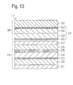
Fig. 13 is a cross sectional view showing an overall configuration of a display apparatus according to a modification example. - With reference to
Figs. 1 to 6 , hereinafter, a touch panel and a display apparatus according to the first embodiment are described. First, with reference toFig. 1 , an overall configuration of the display apparatus is described. - As shown in
Fig. 1 , adisplay apparatus 10 is provided with adisplay panel 20 and atouch panel 30 stacked on thedisplay panel 20 via an adhesive member. Thedisplay panel 20 is a liquid crystal panel including a TFT (thin film transistor)substrate 22 and acolor filter substrate 26 disposed between two deflection plates, i.e., alower deflection plate 21 and anupper deflection plate 27, and aliquid crystal layer 24 sandwiched between theTFT substrate 22 and thecolor filter substrate 26. - A
TFT layer 23 is formed between theTFT substrate 22 and theliquid crystal layer 24. In theTFT layer 23, pixel electrodes as a sub pixel are arranged in a matrix and a TFT which is an active element is provided at every sub pixel. Acolor filter layer 25 including a common electrode is formed between thecolor filter substrate 26 and theliquid crystal layer 24. In thecolor filter 25, in the respective regions divided by the black matrix, a colored layer that converts white light into either red, green or blue faces the sub pixel. - The
touch panel 30 is stacked on theupper deflection plate 27 which is a deflection plate adjacent to thecolor filter substrate 26 in thedisplay panel 20. Thetouch panel 30 is constituted by asensor layer 31 provided with a plurality of electrodes for detecting a change in electrostatic capacitance and acover layer 32 stacked on thesensor layer 31, thecover layer 32 being an operating surface which is a surface of thedisplay apparatus 10. - The
sensor layer 31 is provided with adrive electrode 40 constituted by a plurality of second electrode wirings and asensing electrode 50 constituted by a plurality of first electrode wirings. Thedrive electrode 40 is formed on adrive substrate 33 constituted such as by glass and a resin film. For example, thedrive electrode 40 is formed by etching metal thin film such as copper film or silver film formed on the surface of thedrive substrate 33. Thesensing electrode 50 is formed on asensing substrate 34 constituted such as by glass and a resin film. For example, thesensing electrode 50 is formed by etching metal thin film formed on the front surface of thesensing substrate 34. In other words, in thetouch panel 30, a plurality of first electrode wirings that constitute thesensing electrode 50 are formed on the front surface of thesensing substrate 34 and a plurality of second electrode wirings that constitute thedrive electrode 40 are formed on the reverse surface of thesensing substrate 34. - As for the
sensor layer 31, thesensing substrate 34 with thesensing electrode 50 formed thereon is stacked on thedrive substrate 33 with thedrive electrode 40 formed thereon via an adhesive member so as to form thesensor layer 31. Thesensing substrate 34 serves as a transparent dielectric layer disposed between the second electrode in thedrive electrode 40 and the first electrode in thesensing electrode 50. A select signal that charges/ discharges an electrical charge in thesensing substrate 34 is applied to the second electrode in thedrive electrode 40. A detection signal responding to an amount of electrostatic capacitance between thedrive electrode 40 and thesensing electrode 50 is outputted from thesensing electrode 50, so that position detection can be performed by a controller (not shown). - The
cover layer 32 is formed by tempered glass or synthetic resin and stacked onto thesensor layer 31 via an adhesive member. With reference toFig. 2 , a planar structure of thecolor filter layer 25 in thedisplay panel 20 is described.Fig. 2 is a planar view showing acolor filter substrate 26 with acolor filter layer 25 formed thereon. - As shown in
Fig. 2 , in thecolor filter layer 25, a lattice-like pattern in which the vertical axis and the horizontal axis orthogonally cross with each other is formed by theblack matrix 28. In a rectangular region divided by theblack matrix 28, any one ofcolored layers 29 from among a redcolored layer 29R a greencolored layer 29G and a blue colored layer 29B. The colored layers 29 of the same color are arranged extending along one direction. When thecolored layers 29 of the same color are set to be arranged extending along the Y-direction, the blue colored layer 29B, the greencolored layer 29G and the redcolored layer 29R are arranged repeatedly in this order in the X-direction perpendicular to the Y-direction. Specifically, in thecolor filter layer 25, thecolored layers 29 of the same color are arranged to be extended along the Y-direction to form a stripe shape. On thecolored layer 29, a common electrode which is not shown is formed on the entire surface. - Each of the respective
colored layers 29 is assigned to the sub pixel in theTFT layer 23 and threecolored layers 29 arranged extending along the X-direction constitute a single pixel. Each of the plurality of pixels is arranged extending along the Y-direction so as to form a stripe shape. In thecolor filter layer 25, a lattice-like pattern constituted by a plurality of rectangles arranged in a matrix divides each of the plurality of pixels arranged in a stripe shape to be a pixel pattern corresponding to the pixel arrangement. It should be noted that the pixel width Px which is a width of the pixel in the X-direction, and the pixel width Py which is a width of the pixel in the Y-direction are appropriately set depending on the resolution required for the display apparatus. - With reference to
Figs. 3 to 6 , a planar structure of thedrive electrode 40 and a planar structure of thesensing electrode 50 are described. As shown inFig. 3 , thedrive electrode 40 is constituted by a plurality of drive electrode wirings 41 as a second bending line which is formed as a polygonal line extended along the X-direction. Each of the plurality of drive electrode wirings 41 is arranged to have a constant interval P1 along the Y-direction perpendicular to the X direction. - The plurality of drive electrode wirings 41 are divided every four wirings in the Y-direction and the four drive electrode wirings 41 arranged repeatedly along the Y-direction are connected in parallel with respect to
single terminal portion 42. Each of the plurality ofterminal portions 42 is connected to a selection circuit that selects thedrive electrode wirings 41. The four drive electrode wirings 41 connected to thesingle terminal portion 42 serve as a scanning electrode. - As shown in
Fig. 4 , each of the plurality of drive electrode wirings 41 is a combination of two types oflinear sections 43 having mutually different inclinations and constituted by the two types oflinear sections 43 arranged alternately and repeatedly extending along the X-direction and a bending section 44 (also referred to as a second bending section) serving as a portion at which the two types oflinear sections 43 are coupled. - Each of the plurality of
linear sections 43 has a length D1 extending along a direction along which thelinear section 43 extends. Onelinear section 43a in the two types oflinear sections 43 has an inclination of +θ1 degree with respect to the reference line A1 which is a linear line extending along the X-direction and the otherlinear section 43b has an inclination of -θ1 degree with respect to the reference line A1. Regarding each of the plurality ofdrive electrode wirings 41, onedrive electrode wiring 41 is formed to have a shape in which the onedrive electrode 41 is translated in the Y-direction. The bendingsections 44 each having a portion at which thelinear section 43a and thelinear section 43b are coupled are arranged on a linear line L1 extending along the Y-direction in the plurality ofdrive electrode wirings 41. - The length D1 of the
linear section 43 satisfies the following equation 1 and is set such that the length Dx of thelinear section 43 in the X-direction is the same as the interval P1. The interval P1, an angle formed between the reference line A1 and thelinear section 43 are appropriately set depending on the detection accuracy required for thetouch panel 30 and the width of the pixel width Px and Py of thedisplay panel 20.
In onedrive electrode wiring 41, an auxiliary line B1 and an auxiliary line B2 are set as a linear line to connect the bendingsections 44 arranged extending along the X-direction and a region sandwiched by the auxiliary line B1 and the auxiliary line B2 is set as a bending region R1. In this case, mutually adjacent bending regions R1 of the drive electrode wirings 41 are arranged extending along the Y-direction with intervals therebetween and the length D1 of thelinear section 43, the interval P1 and the angle θ1 are set to avoid overlapping with each other. Here, in a case where the mutually adjacent bending regions R1 mutually overlap in the Y-direction, an operation position in the operation surface is detected by two mutually adjacent drive electrode wirings 41 so that the accuracy of detecting the operation position is degraded. In this respect, according to a configuration in which the mutually adjacent bending regions R1 are arranged extending along the Y-direction with intervals therebetween, degradation of the accuracy when detecting the operation position can be avoided. - As shown in
Fig. 5 , as for thesensing electrode 50, compared to thedrive electrode 40, the direction where each of the plurality of electrode wirings is extended and the direction where each of the plurality of electrode wirings are repeatedly arranged are different from that of thedrive electrode 40. In other words, thesensing electrode 50 is constituted by a plurality ofsensing electrode wirings 51 as a first bending line formed as a polygonal line extended along the Y-direction. The plurality ofsensing electrode wirings 51 are arranged extending along the X-direction with constant intervals P1 therebetween. The interval P1 located between mutually adjacentsensing electrode wirings 51 may be the same as the interval P1 of the mutually adjacent drive electrode wirings 41 or may be different from the one of the mutually adjacentdrive electrode wirings 41. The same applies to the length D1 of thelinear section 43 and the angle θ. - The plurality of
sensing electrode wirings 51 are divided every four wirings along the X-direction and the foursensing electrode wirings 51 arranged repeatedly along the X-direction are connected in parallel with respect to onesingle terminal portion 52. Each of the plurality ofterminal portions 52 is connected to a detection circuit that detects a change in electrostatic capacitance. The foursensing electrode wirings 51 connected to thesingle terminal portion 52 serve as a detection electrode. - As shown in
Fig. 6 , each of the plurality ofsensing electrode wirings 51 is a combination of two types oflinear sections 53 having mutually different inclinations and constituted by the two types oflinear sections 53 arranged alternately and repeatedly extending along the Y-direction and abending section 54 as a first bending section serving as a portion at which the two types oflinear sections 53 are coupled. - Each of the plurality of
linear sections 53 has a length D1 along a direction where thelinear section 53 extends. Onelinear section 53a in the two types oflinear sections 53 has an inclination of +θ1 degree with respect to the reference line A2 which is a linear line extending along the Y-direction and the otherlinear section 53b has an inclination of -θ1 degree with respect to the reference line A2. Regarding each of the plurality ofsensing electrode wirings 51, onesensing electrode wiring 51 is formed to have a shape in which the onesensing electrode wiring 51 is translated in the X-direction. The bendingsections 54 each having a portion at which thelinear section 53a and thelinear section 53b are coupled are arranged on a linear line L2 extending along the X-direction in the plurality ofsensing electrode wirings 51. - The length D1 of the
linear section 53 satisfies the following equation 2 and is set such that the length Dy of thelinear section 53 in the Y-direction is the same as the interval P1. The interval P1 and an angle formed between the reference line A2 and thelinear section 53 are appropriately set depending on the detection accuracy required for thetouch panel 30 and the width of the pixel width Px and Py of thedisplay panel 20.
In onesensing electrode wiring 51, a linear line that connects the bendingsections 54 arranged extending along the Y-direction is set as an auxiliary line B3 and an auxiliary line B4, and a region sandwiched by the auxiliary line B3 and the auxiliary line B4 is set as a bending region R2. In this case, mutually adjacent bending regions R2 of thesensing electrode wirings 51 are arranged extending along the X-direction with intervals therebetween and the length D1 of thelinear section 53, the interval P1 and the angle θ1 are set to avoid overlapping each other. Here, in a case where the mutually adjacent bending regions R2 mutually overlap in the X-direction, two mutually adjacentsensing electrode wirings 51 are assigned to one operation position so that an accuracy for detecting the operation position is degraded. In this respect, according to a configuration in which the mutually adjacent bending regions R2 are arranged extending along the X-direction with intervals therebetween, degradation of the accuracy of detecting the operation position can be avoided. - With reference to
Fig. 7 , an electrode pattern formed by thedrive electrode 40 and thesensing electrode 50 is described. InFig. 7 , for convenience of explanation, viewing from the front surface of thesensing substrate 34 which is a transparent dielectric layer, that is, viewing from the surface of thedisplay apparatus 10, each of the plurality ofsensing electrodes 50 arranged above thesensing substrate 34 are shown as white hollow lines and each of the plurality ofdrive electrode 40 arranged below thesensing substrate 34 are shown as solid lines. - As shown in
Fig. 7 , in the electrode pattern, each of the plurality of bendingsections 44 of thedrive electrode wiring 41 are arranged at locations with which none ofsensing electrode wirings 51 are overlapped and face the interval between the two mutually adjacentsensing electrode wirings 51. Each of the plurality of bendingsections 54 of thesensing electrode wiring 51 are arranged at locations with which none of drive electrode wirings 41 are overlapped and face the interval between the two mutually adjacentdrive electrode wirings 41. - Specifically, the
drive electrode 40 and thesensing electrode 50 are arranged such that the bending section of the electrode wiring at one electrode is disposed at a position not to overlap with the electrode wiring at the other electrode. Each of thedrive electrode wirings 41 and each of thesensing electrode wirings 51 are overlapped at thelinear section 43 of thedrive electrode wiring 41 and thelinear section 53 of thesensing electrode wirings 51. With two mutually adjacentdrive electrode wirings 41 and two mutually adjacentsensing electrode wirings 51, four types of octagons having two reflex angles among interior angles thereof are formed. When viewing from the front surface of thesensing substrate 34, an electrode pattern is formed such that these four types of octagons are arranged extending along the X-direction and the Y-direction. - Next, effects of the above-described
touch panel 30 and thedisplay apparatus 10 will be described. - In the
touch panel 30, an electrode pattern is formed by thedrive electrode 40 and thesensing electrode 50, in which four types of octagons are arranged extending along the X-direction and the Y-direction. Therefore, compared to a conventional electrode pattern having rectangles arranged in a matrix, variation will happen on the regularity of the pattern. - For example, in an octagon M1, a vertex V1 protruded towards the -Y-direction is formed by the bending
section 44 of onedrive electrode wiring 41 and a vertex V2 protruded towards the -Y-direction is formed by the bendingsection 44 of the otherdrive electrode wiring 41. Meanwhile, in an octagon M2 adjacent to the octagon M1, a vertex V3 protruded towards +Y-direction is formed by the bendingsection 44 of onedrive electrode wiring 41 and a vertex V4 protruded towards +Y-direction is formed by the bendingsection 44 of the otherdrive electrode wiring 41. In the octagon M1 and the octagon M2 which are adjacent to each other in the X-direction, the vertex V1 and the vertex V3 formed by onedrive electrode wiring 41 are formed at mutually different positions in the Y-direction. Moreover, in the octagon M1 and the octagon M2 which are mutually adjacent in the X-direction, the vertex V2 and the vertex V4 formed by the otherdrive electrode wiring 41 are formed at mutually different positions in the Y-direction. - For example, in an octagon M1, a vertex V5 protruded towards the + X-direction is formed by the bending
section 54 of onesensing electrode wiring 51 and a vertex V6 protruded towards +X-direction is formed by the bendingsection 54 of the othersensing electrode wiring 51. Meanwhile, in an octagon M3 adjacent to the octagon M1, a vertex V7 protruded towards the -X-direction is formed by the bendingsection 54 of onesensing electrode wiring 51 and vertex V8 protruded towards the -X-direction is formed by the bendingsection 54 of the othersensing electrode wiring 51. In the octagon M1 and the octagon M3 which are adjacent to each other in the Y-direction, the vertex V5 and the vertex V7 formed by onesensing electrode 51 are formed at mutually different positions in the X-direction. Moreover, in the octagon M1 and the octagon M3 which are mutually adjacent in the Y-direction, the vertex V6 and the vertex V8 formed by the othersensing electrode wiring 51 are formed at mutually different positions in the X-direction. - As a result, using the electrode pattern formed by the
drive electrode 40 and thesensing electrode 50, compared to an electrode pattern in which rectangles are arranged extending along the X-direction and the Y-direction, the regularity of the pattern is lower in both X-direction and Y-direction. - Here, when an electrode pattern in which rectangles are arranged extending along the X-direction and the Y-direction and a pixel pattern in which rectangles are arranged extending along the X-direction and the Y-direction are overlapped, patterns having high regularity are overlapped with each other, whereby interference fringes is occurred due to shift of the period thereof. On the other hand, when using an electrode pattern formed in the
touch panel 30, since the regularity of the pattern thereof is low compared to the above-described electrode pattern, occurrence of the interference fringes is reduced when thedisplay panel 20 and the touch panel are stacked. - In other words, in the electrode pattern in which rectangles are arranged extending along the X-direction and the Y-direction, the area that one electrode wiring occupies is limited to only an area corresponding to the line width of the electrode wiring in a direction where the electrode wiring is arranged. On the other hand, when using an electrode pattern formed in the
touch panel 30, since the electrode wiring is a bending line, the area that one electrode wiring occupies is widened to be a bending region R1 or a bending region R2 in a direction where the electrode wirings are arranged. Accordingly, when thedisplay panel 20 and thetouch panel 30 are overlapped, a contour of the pattern formed by a pixel pattern of thedisplay panel 20 and an electrode pattern of thetouch panel 30 becomes unclear. As a result, the occurrence of interference fringes can be reduced. - Since the occurrence of interference fringes is reduced, degradation of the image quality of the
display apparatus 10 is avoided. Moreover, to reduce the interference fringes, it is not necessary to provide such as films in thedisplay apparatus 10. Hence, the manufacturing steps for thedisplay apparatus 10 can be simplified. In particular, since the regularity of the electrode pattern formed in thetouch panel 30 is not high, displacement of positions between thedrive electrode 40 and thesensing electrode 50 and displacement of positions between thetouch panel 30 and thedisplay panel 20 are less likely to influence the effects of reducing the interference fringes. Therefore, when thedrive electrode 40 and thesensing electrode 50 are stacked or thetouch panel 30 and thedisplay panel 20 are stacked, alignment of positions of the objects to be stacked does not require such high accuracy, so that the display apparatus can easily be manufactured. Further, since the electrode pattern formed in thetouch panel 30 is configured by a combination of linear sections, compared to an electrode pattern including bending lines, the electrode pattern can easily be designed and manufactured. - In an electrode pattern in which rectangles or rhobmbuses are arranged extending along the X-direction and the Y-direction, undulations or interference fringes occur in the electrode pattern because of slight shifts in overlap between the drive electrode and the sensing electrode or because of slight errors in intervals between the electrode wirings. However, according to the electrode pattern formed in the
touch panel 30, compared to an electrode pattern in which rectangles or rhobmbuses are arranged extending along the X-direction and the Y-direction, the regularity of the pattern in both X-direction and the Y-direction becomes low so that undulations or interference fringes in the electrode pattern can be reduced. - A touch panel according to an example was produced in which dimensions of an electrode pattern were set as the following electrode condition. Also, a display panel according to the example was produced in which dimensions of a pixel pattern were set as the following pixel condition. The touch panel and the display panel were stacked so as to produce an example display apparatus. An evaluation was applied to the display apparatus in which occurrence of interference of fringes was evaluated by a visual inspection as a sensory evaluation. As a result, occurrence of interference fringes was appropriately reduced within a range that satisfies the following electrode condition and the pixel conditions.
-
- Interval P1: ranges from 0.4 mm to 0.64 mm
- Angle θ1: ranges from 27. 5 degrees to 40.0 degrees
- Length D1: D1 = P1/ cos θ1
- Pixel width Px, Pixel width Py : (84 µm, 252 µm), (60 µm, 179 µm)
: (83 µm, 248 µm), (91 µm, 273 µm)
As described above, according to the first embodiment, following effects can be obtained. - (1) Since the regularity is low in the electrode pattern formed in the
touch panel 30, the occurrence of interference fringes is reduced in a configuration in which adisplay panel 20 and thetouch panel 30 are stacked on each other. - (2) Since the regularity is low in a lattice-like electrode pattern formed by the
drive electrode 40 and thesensing electrode 50, undulation or interference fringes in the electrode pattern can be reduced. - (3) When the
touch panel 30 and thedisplay panel 20 are stacked, since positions of objects to be stacked do not require high alignment accuracy, thedisplay apparatus 10 can easily be manufactured. - (4) Since the electrode pattern formed in the
touch panel 30 is a combination of linear sections, compared to a configuration in which the electrode pattern includes complicated patterns, the electrode pattern can easily be designed and manufactured. - With reference to
Figs. 8 to 10 , regarding a touch panel and a display apparatus according to the second embodiment, differences from the one of the first embodiment will mainly be described. In the second embodiment, planar structures of the drive electrode and the sensing electrode differ from that of the first embodiment. Accordingly, planar structures of respective electrode wirings will mainly be described and configurations similar to the first embodiment are labeled with the same reference numbers and explanation thereof is omitted. - As shown in
Fig. 8 , adrive electrode 45 is constituted by a plurality of drive electrode wirings 46 as a second bending line which is formed as a polygonal line extended along the X-direction. Each of the plurality of drive electrode wirings 56 is arranged extending along the Y-direction perpendicular to the X-direction with a constant interval P2. - Each of the plurality of drive electrode wirings 46 is a combination of two types of linear sections having mutually different inclinations and constituted by the two types of
linear sections 47 arranged alternately and repeatedly extending along the X-direction and by abending section 48 as a second bending section serving as a portion at which the two types oflinear sections 47 are coupled. - Each of the
linear sections 47 has a length D2 along a direction where thelinear section 47 extends. One linear section 47a in the two types oflinear sections 47 has an inclination of +θ2 with respect to the reference line A1 which is a linear line extending along the X-direction and the other linear section 47b has an inclination of -θ2 degree with respect to the reference line A1. Regarding each of the plurality ofdrive electrode wirings 46, onedrive electrode wiring 46 is formed to have a shape in which the onedrive electrode wiring 46 is translated in the Y-direction. The bendingsections 48 each having a portion at which the linear section 47a and the linear section 47b are coupled are arranged on a linear line L1 extending along the Y-direction in the plurality ofdrive electrode wirings 46. - The length D2 of the
linear section 47 satisfies the following equation 3 and is set such that the length Dx of thelinear section 47 in the X-direction is longer than the interval P2. The interval P2 and an angle formed between the reference line A1 and thelinear section 47 are appropriately set depending on the detection accuracy required for thetouch panel 30 and the width of the pixel width Px and Py.
In onedrive electrode wiring 46, an auxiliary line B5 and an auxiliary line B6 are set to connect the bendingsections 48 arranged extending along the X-direction and a region sandwiched by the auxiliary line B5 and the auxiliary line B6 is set as a bending region R3. In this case, also in the present embodiment, mutually adjacent bending regions R3 of the drive electrode wirings 46 are arranged extending along the Y-direction with intervals therebetween and the length D2 of thelinear section 47, the interval P2 and the angle θ2 are set to avoid overlapping each other. - As shown in
Fig. 9 , as for thesensing electrode 55, compared to thedrive electrode 45, the direction where the plurality of electrode wirings are extended and the direction where each of the plurality of the electrode wirings are arranged are different from thedrive electrode 45. In other words, thesensing electrode 55 is constituted by a plurality ofsensing electrode wirings 56 as a first bending line formed as a polygonal line extended along the Y-direction. The plurality ofsensing electrode wirings 56 are arranged extending along the X-direction with constant intervals P2 therebetween. The interval P2 located between mutually adjacentsensing electrode wirings 56 may be the same as the interval P2 of the mutually adjacentdrive electrode wirings 46. - Each of the plurality of
sensing electrode wirings 56 is also a combination of two types oflinear sections 57 having mutually different inclinations and constituted by the two types oflinear sections 57 arranged alternately and repeatedly extending along the Y-direction and abending section 58 as a first bending section serving as a portion at which the two types oflinear sections 53 are coupled. - Each of the plurality of
linear sections 57 has a length D2 along a direction where thelinear section 57 extends. One type oflinear section 57a of the two types oflinear sections 57 has an inclination of +θ2 degrees with respect to the reference line A2 which is a linear line extending along the Y-direction and the otherlinear section 57b has an inclination of -θ2 degrees with respect to the reference line A2. Regarding each of the plurality ofsensing electrode wirings 56, onesensing electrode wiring 56 is formed to have a shape in which the onesensing electrode wiring 56 is translated in the X-direction. The bendingsections 58 each having a portion at which thelinear section 57a and thelinear section 57b are coupled are arranged on a linear line L2 extending along the X-direction in the plurality ofsensing electrode wirings 56. - The length D2 of the
linear section 57 satisfies the following equation 4 and is set such that the length Dy of thelinear section 57 in the Y-direction is longer than the interval P2. The interval P2 and an angle formed between the reference line A2 and thelinear section 57 are appropriately set depending on the detection accuracy required for thetouch panel 30 and the width of the pixel width Px and Py of thedisplay panel 20.
In onesensing electrode wiring 56, an auxiliary line B7 and an auxiliary line B8 are set to connect the bendingsections 58 arranged extending along the Y-direction and a region sandwiched by the auxiliary line B7 and the auxiliary line B8 is set as a bending region R4. In this case, also in the present embodiment, mutually adjacent bending regions R4 of theelectrode wirings 56 are arranged extending along the X-direction with intervals therebetween and the length D2 of thelinear section 57, the interval P2 and the angle θ2 are set to avoid overlapping from each other. - With reference to
Fig. 10 , an electrode pattern formed by thedrive electrode 45 and thesensing electrode 55 is described. InFig. 10 , for convenience of explanation, viewing from the surface of thedisplay apparatus 10, each of the plurality ofsensing electrodes 55 arranged above thesensing substrate 34 are shown as white hollow lines and each of the plurality ofdrive electrode 45 arranged below thesensing substrate 34 are shown as solid lines. - As shown in
Fig. 10 , in the electrode pattern, at least a part of the plurality of bendingsections 48 of thedrive electrode wiring 46 are arranged at locations with which none ofsensing electrode wirings 56 are overlapped and face the interval between the two mutually adjacentsensing electrode wirings 56. At least a part of the plurality of bendingsections 58 of thesensing electrode wiring 56 are arranged at locations with which none of drive electrode wirings 46 are overlapped and face the interval between the two mutually adjacentdrive electrode wirings 46. - According to the configuration in which the above described equations 3 and 4 are satisfied, a quadrangle pattern divided by two mutually adjacent
linear sections 47 and two mutually adjacentlinear sections 57 is included in a part of electrode pattern. Also, according to the configuration in which the above described equations 3 and 4 are satisfied, a point P at which thebending section 48 in thedrive electrode wiring 46 and thesensing electrode 56 are overlapped, constitutes a part of electrode wiring. Moreover, according to the configuration in which the above described equations 3 and 4 are satisfied, a point P at which thebending section 58 in thesensing electrode wiring 56 and thedrive electrode wiring 46 are overlapped constitutes a part of electrode wiring. In a pattern in which a polygon vertex is a point P, the number of vertexes is less than eight. - Eventually, the electrode pattern formed in the
touch panel 30 includes two or more types of polygons having mutually different number of vertexes within the range of 4 to 8 vertexes inclusive. The electrode pattern formed in thetouch panel 30 also includes a plurality of polygons in which the number of vertexes is the same and shapes are mutually different. - Next, effects of the above-described
touch panel 30 and thedisplay apparatus 10 will be described as follows. In thetouch panel 30, a lattice-like electrode pattern is formed by thedrive electrode 45 and thesensing electrode 55. The lattice-like electrode pattern is constituted by a polygon having 4 to 8 vertexes. Therefore, compared to a conventional type electrode pattern having a lattice-like pattern in which rectangles are arranged in a matrix, or an electrode pattern in which octagons described in the first embodiment are arranged, the regularity of the pattern becomes even lower. As a result, occurrence of the interference fringes can be further reduced when thedisplay panel 30 and thetouch panel 30 are overlapped. - As described above, according to the second embodiment, in addition to effects described in the above (1) to (4), the following effects can be obtained.
- (5) The electrode pattern formed in the
touch panel 30 includes two or more types of polygons having mutually different numbers of vertexes among polygons having 4 to 8 vertexes so that the regularity of the electrode pattern becomes low. Therefore, occurrence of interference fringes can be further reduced. - (6) The electrode pattern formed in the
touch panel 30 includes polygons having the same number of vertexes and mutually different shapes so that the regularity of the electrode pattern becomes even lower. - The above-described embodiments can be implemented, being modified as follows.
- The bending section may include either electrode wirings or sensing electrode wirings. As shown in
Fig. 11 , for example, thedrive electrode 64 may be constituted by a plurality of drive electrode wirings 65 which are linear lines extended along the X-direction and thesensing electrode 50 may be constituted, similar to that of the first embodiment, by a plurality ofsensing electrode wirings 51 havinglinear sections 53 and bendingsections 54. In this case, each of the plurality of bendingsections 54 in thesensing electrode wirings 51 is located to face the interval between two mutually adjacentdrive electrode wirings 65 and not to overlap with thedrive electrode 65. According to these configurations, similar effects as described in the above (1) to (4) can be obtained. - The sensing electrode wiring may be constituted by a plurality of sensing electrode wirings extended along the Y-direction. The drive electrode may be constituted by, similar to the first embodiment, a plurality of drive electrode wirings 41 having the
linear section 43 and thebending section 44. In this case, each of the plurality of bendingsections 44 in the drive electrode wirings 41 faces the interval between two mutually adjacent sensing electrode wirings and is located at a portion not to overlap with the sensing electrode wiring. - A part of the plurality of drive electrode may be a linear line extended along the X-direction or a part of the plurality of sensing electrode may be a linear line extended along the Y-direction. In other words, as long as an electrode wiring having a bending section is included in the electrode wiring that constitutes the drive electrode and the sensing electrode, other electrode wiring may not include the bending section. According to these configurations, similar effects as described in the above (1) to (4) can be obtained.
- The length of an interval between mutually adjacent drive electrode wirings and the length of an interval between mutually adjacent sensing electrode wirings may be different from each other. Further, an angle formed between the drive electrode wiring and the reference line A1 and an angle formed between the sensing electrode wiring and the reference line A2 may be different from each other. Moreover, a length of the linear section of the drive electrode wiring and a length of the linear section of the sensing electrode wiring may be different from each other. Furthermore, an angle formed between the drive electrode wiring and the sensing electrode wiring may be an angle other than 90 degrees, when viewing from the front surface of the transparent dielectric layer. That is, when viewing from the of the transparent dielectric layer, a configuration in which each of the plurality of first electrode wirings crosses each of the plurality of second electrode wirings and at least a part of the plurality of bending sections faces an interval between the second electrode wirings may be employed.
- In the drive electrode, the length of the interval between mutually adjacent drive electrode wirings may have two or more mutually different values and an absolute value of the angle formed between the linear section and the reference line A1 may have two or more mutually different values. Further, in the drive electrode, the length of the linear section of the drive electrode wirings may have two or more mutually different values.
- In the sensing electrode, the length of the interval between mutually adjacent sensing electrode wirings may have two or more mutually different values and an absolute value of the angle formed between the sensing electrode wiring and the reference line A2 may have two or more mutually different values. Further, in the drive electrode, the length of the linear section of the sensing electrode wirings may have two or more mutually different values.
- In one drive electrode wiring, the length of the interval between mutually adjacent drive electrode wirings may have two or more mutually different values and an absolute value of the angle formed between the linear section and the reference line A1 may have two or more mutually different values. Further, in the drive electrode wiring, the length of the linear section of the drive electrode wirings may have two or more mutually different values.
- In the sensing electrode wiring, the length of the interval between mutually adjacent sensing electrode wirings may have two or more mutually different values and an absolute value of the angle formed between the sensing electrode wiring and the reference line A2 may have two or more mutually different values. Further, in the drive electrode wiring, length of the linear section of the drive electrode wirings may have two or more mutually different values.
- In one electrode wiring, a part of the plurality of bending sections may be a curve having a curvature and the rest of the plurality of bending sections may be a coupled portion of two linear sections. In two electrodes, a part of the plurality of electrode wirings may be formed such that the bending section is a curve having a curvature and rest of the plurality of electrode wirings may be formed such that the bending section is a coupled portion of two linear sections. In a configuration in which a part of the plurality of bending sections is a curve having a curvature, an electrode pattern formed in the
touch panel 30 is constituted by a polygon different from a quadrangle and a pseudo polygon. According to these configurations, since the regularity of the electrode pattern is low, similar effects as described in the above (1) to (6) can be obtained. - According to the first embodiment, a part of the plurality of drive electrode wirings may have a configuration that satisfies equation 3 or a part of the plurality of sensing electrode wirings may have a configuration that satisfies the equation 4. In at least a part of the plurality of electrode wirings, a relationship among length of the linear section D1, the interval P1, the angle θ1 may satisfy a condition D1 cosθ1 < P1. Also, in at least some of the plurality of electrode wirings, relationship among length of the linear section D2, the interval P2, the angle θ2 may satisfy D2 cosθ2 < P2. In other words, when viewing from the front surface of the transparent dielectric layer, a configuration in which each of the plurality of first electrode wirings crosses each of the plurality of second electrode wirings and at least a part of the plurality of bending sections faces the interval of the second electrode wirings may be used.
- According to the first and second embodiments, the
drive electrode 40 is formed on the front surface of thedrive substrate 33 and thesensing electrode 50 is formed on the front surface of thesensing substrate 34. Alternatively, in the manufacturing step of thetouch panel 30, one transparent dielectric layer may be used for a substrate. The drive electrode may be formed on the reverse side of the substrate and the sensing electrode may be formed on the front surface of the substrate. For example, as shown inFig. 12 , thesensing electrode 50 may be formed on the front surface of thesensing substrate 34 and thedrive electrode 40 may be formed on the reverse surface of thesensing substrate 34. - In the
touch panel 30, a configuration in which the drive electrode and the sensing electrode sandwiches a transparent dielectric layer which is different from a substrate used in the manufacturing step of the drive electrode and the sensing electrode, may be employed. For example, as shown inFig. 13 , thesensing electrode 50 may be formed on the front surface of thesensing substrate 34 and thedrive electrode 40 may be formed on the reverse surface of thedrive substrate 33 and then thesensing substrate 34 may be stacked on thedrive substrate 33 via an adhesive member. - The sensing electrode wiring, as a second electrode wiring, may be formed on the reverse surface of the transparent dielectric layer and the drive electrode wiring, as a first electrode wiring, may be formed on the front surface of the transparent dielectric layer. In other words, the
touch panel 30 may be a configuration in which a plurality of first electrode wirings are arranged with intervals along the first direction on the front surface of the transparent dielectric layer, and a plurality of second electrode wirings are arranged with intervals along the second direction on the reverse surface of the transparent dielectric layer. - The pixel arrangement in the
display panel 20 is not limited to the stripe shape. Instead, the pixel arrangement may be a mosaic shape or a delta shape. While thedisplay panel 20 is provided with pixels arranged periodically, a periodical pattern is formed by a portion that divides pixels. In a display apparatus having a display panel and atouch panel 30 which are stacked on each other, occurrence of interference fringe is reduced. - A display element used for the
display panel 20 is not limited to a liquid crystal element. However, for example, a self-luminous element such as organic EL (electroluminescent) device may be used as a display element. In other words, thedisplay panel 20 may have a configuration in which each of the plurality of pixels is divided to form a lattice shape. While the display element has a configuration in which each of the plurality of pixels is divided to form a lattice shape, a periodical pattern is formed in the display panel. Therefore, in a display apparatus having a display panel and atouch panel 30 which are stacked on each other, occurrence of interference fringe is reduced. -
- 10: display apparatus
- 20: display panel
- 21: lower deflection plate
- 22: TFT substrate
- 23: TFT layer
- 24: liquid crystal layer
- 25: color filter layer
- 26: color filter substrate
- 27: upper deflection plate
- 28: black matrix
- 29: colored layer
- 30: touch panel
- 31: sensor layer
- 32: cover layer
- 33: drive substrate
- 34: sensing substrate
- 40, 45, 64: drive electrode
- 41, 46, 65: drive electrode wiring
- 42, 52: terminal portion
- 43, 43a, 43b, 47, 47b, 53, 53a, 53b, 57, 57a, 57b: linear section
- 44, 48, 54, 58: bending section
- 50, 55: sensing electrode
- 51, 56: sensing electrode wiring
Claims (12)
- A touch panel comprising:a transparent dielectric layer;a plurality of first electrode wirings arranged, on a front surface of the transparent dielectric layer, repeatedly along a first direction with intervals therebetween; anda plurality of second electrode wirings arranged, on a reverse surface of the transparent dielectric layer, repeatedly along a second direction with intervals therebetween,whereinat least a part of the plurality of first electrode wirings is a bending line having a plurality of bending sections arranged repeatedly in a direction along which the first electrode wiring extends;when viewing from the front surface of the transparent dielectric layer, each of the plurality of first electrode wirings crosses each of the plurality of second electrode wirings andat least a part of the plurality of bending sections faces the intervals between the second electrode wirings.
- The touch panel according to claim 1, wherein
the transparent dielectric layer is a first transparent dielectric layer;
the touch panel further comprises a second transparent dielectric layer; and
the plurality of second electrode wirings are formed on a front surface of the second transparent dielectric layer. - The touch panel according to claim 1, wherein
the transparent dielectric layer includes plural layers of transparent dielectric layer . - The touch panel according to any one of claims 1 to 3, wherein
the bending line is a polygonal line formed by a plurality of linear sections combined with each other; and
when viewing from the surface of the transparent dielectric layer, a pattern divided by two mutually adjacent first electrode wirings and two mutually adjacent second electrode wirings includes a polygon having five or more vertexes. - The touch panel according to any one of claims 1 to 4, wherein
the bending line is a polygonal line formed by a plurality of linear sections combined with each other; and
when viewing from the front surface of the transparent dielectric layer, a pattern divided by two mutually adjacent first electrode wirings and two mutually adjacent second electrode wirings includes two or more types of polygons having mutually different number of vertexes among polygons having four to eight vertexes. - The touch panel according to any one of claims 1 to 5, wherein
the bending section is a first bending section;
the bending line is a first bending line;
at least a part of the plurality of second electrode wirings is a second bending line having a plurality of second bending sections arranged repeatedly extending along a direction where the second electrode wiring extends; and
when viewing from the front surface of the transparent dielectric layer, at least a part of the plurality of second bending lines faces the intervals between the first electrode wirings. - A display apparatus provided with a display panel having pixels arranged in matrix and a touch panel stacked on the display panel, the touch panel comprising:a transparent dielectric layer;a plurality of first electrode wirings arranged, on a front surface of the transparent dielectric layer, repeatedly along a first direction with intervals therebetween; anda plurality of second electrode wirings arranged, on a reverse surface of the transparent dielectric layer, repeatedly along a second direction with intervals therebetween, whereinat least a part of the plurality of first electrode wirings is a bending line having a plurality of bending sections arranged repeatedly in a direction along which the first electrode wiring extends;when viewing from the front surface of the transparent dielectric layer, each of the plurality of first electrode wirings crosses each of the plurality of second electrode wirings andat least a part of the plurality of bending sections faces the intervals between the second electrode wirings.
- The display apparatus according to claim 7, wherein
the transparent dielectric layer is a first transparent dielectric layer;
the touch panel further comprises a second transparent dielectric layer; and
the plurality of second electrode wirings are formed on a front surface of the second transparent dielectric layer. - The display apparatus according to claim 7, wherein
the transparent dielectric layer includes plural layers of transparent dielectric layer . - The display apparatus according to any one of claims 7 to 9, wherein
the bending line is a polygonal line formed by a plurality of linear sections combined from each other; and
when viewing from the front surface of the transparent dielectric layer, a pattern divided by two mutually adjacent first electrode wirings and two mutually adjacent second electrode wirings includes a polygon having five or more vertexes. - The display apparatus according to any one of claims 7 to 10,
wherein the bending line is a polygonal line formed by a plurality of linear sections combined from each other; and
when viewing from the front surface of the transparent dielectric layer, a pattern divided by two mutually adjacent first electrode wirings and two mutually adjacent second electrode wirings includes two or more types of polygons having mutually different number of vertexes among polygons having four to eight vertexes. - The display apparatus according to any one of claims 7 to 11,
the bending section is a first bending section;
the bending line is a first bending line;
at least a part of the plurality of second electrode wirings is a second bending line having a plurality of second bending sections arranged repeatedly along a direction where the second electrode wiring extends; and
when viewing from the front surface of the transparent dielectric layer, at least a part of the plurality of second bending lines faces the intervals between the first electrode wirings.
Applications Claiming Priority (2)
| Application Number | Priority Date | Filing Date | Title |
|---|---|---|---|
| JP2013011262 | 2013-01-24 | ||
| PCT/JP2014/051475 WO2014115831A1 (en) | 2013-01-24 | 2014-01-24 | Touch panel and display device |
Publications (2)
| Publication Number | Publication Date |
|---|---|
| EP2950186A1 true EP2950186A1 (en) | 2015-12-02 |
| EP2950186A4 EP2950186A4 (en) | 2016-09-28 |
Family
ID=51227620
Family Applications (1)
| Application Number | Title | Priority Date | Filing Date |
|---|---|---|---|
| EP14742944.3A Withdrawn EP2950186A4 (en) | 2013-01-24 | 2014-01-24 | TOUCH PANEL, AND DISPLAY DEVICE |
Country Status (7)
| Country | Link |
|---|---|
| US (1) | US20150331526A1 (en) |
| EP (1) | EP2950186A4 (en) |
| JP (2) | JP5930076B2 (en) |
| KR (1) | KR20150108356A (en) |
| CN (1) | CN104798020A (en) |
| TW (1) | TWI550450B (en) |
| WO (1) | WO2014115831A1 (en) |
Families Citing this family (23)
| Publication number | Priority date | Publication date | Assignee | Title |
|---|---|---|---|---|
| WO2014115831A1 (en) * | 2013-01-24 | 2014-07-31 | 凸版印刷株式会社 | Touch panel and display device |
| JP2014191575A (en) * | 2013-03-27 | 2014-10-06 | Dainippon Printing Co Ltd | Electrode substrate for touch panel, touch panel, and image display device |
| CN105469732B (en) * | 2014-09-05 | 2019-02-05 | 联想(北京)有限公司 | Display device and electronic equipment |
| JP2016126730A (en) * | 2015-01-08 | 2016-07-11 | 凸版印刷株式会社 | Touch sensor electrodes, touch panel, and display device |
| JP2016126731A (en) * | 2015-01-08 | 2016-07-11 | 凸版印刷株式会社 | Touch sensor electrode, touch panel, and display device |
| CN104536634A (en) | 2015-01-26 | 2015-04-22 | 京东方科技集团股份有限公司 | Touch screen and display device |
| CN104638016A (en) | 2015-01-28 | 2015-05-20 | 京东方科技集团股份有限公司 | Thin film transistor and manufacturing method of thin film transistor, array substrate and manufacturing method of array substrate, and display device |
| JP2016173697A (en) * | 2015-03-17 | 2016-09-29 | 富士フイルム株式会社 | Transparent conductive film for touch panel and touch panel |
| CN104978070A (en) * | 2015-07-27 | 2015-10-14 | 苏州触动电子科技有限公司 | Touch control film capable of eliminating diffraction |
| CN105138186B (en) * | 2015-10-08 | 2018-01-23 | 京东方科技集团股份有限公司 | A kind of touch electrode structure, touch-screen and display device |
| CN107562249B (en) * | 2016-07-01 | 2024-04-30 | 瀚宇彩晶股份有限公司 | Touch display device |
| US10386975B2 (en) * | 2016-08-30 | 2019-08-20 | Tactual Labs Co. | Capacitive sensor |
| JP2018049557A (en) * | 2016-09-23 | 2018-03-29 | 富士通コンポーネント株式会社 | Touch panel |
| CN109426399B (en) * | 2017-09-05 | 2022-03-01 | 瀚宇彩晶股份有限公司 | Touch control display device |
| JP7039248B2 (en) | 2017-10-20 | 2022-03-22 | 株式会社Vtsタッチセンサー | Conductive film, touch panel, and display device |
| CN108170307A (en) * | 2017-11-30 | 2018-06-15 | 云谷(固安)科技有限公司 | A kind of touch panel and touch control display apparatus |
| US10928951B2 (en) * | 2018-05-31 | 2021-02-23 | Japan Aviation Electronics Industry, Limited | Touch panel having high resistance to static electricity |
| CN110767825B (en) * | 2018-08-06 | 2022-06-21 | 云谷(固安)科技有限公司 | Display panel, display screen and display terminal |
| JP7281940B2 (en) * | 2019-03-28 | 2023-05-26 | 株式会社ジャパンディスプレイ | Display device with detector |
| JP7478151B2 (en) | 2019-07-05 | 2024-05-02 | 株式会社ワコム | Position detection sensor and electronic device |
| TWI708173B (en) * | 2019-08-26 | 2020-10-21 | 友達光電股份有限公司 | Touch panel |
| CN115777093A (en) * | 2020-08-27 | 2023-03-10 | 富士胶片株式会社 | Conductive member for touch panel and touch panel |
| CN114284304B (en) * | 2021-12-30 | 2025-04-15 | 上海天马微电子有限公司 | Display module and display device |
Family Cites Families (26)
| Publication number | Priority date | Publication date | Assignee | Title |
|---|---|---|---|---|
| JPH11110115A (en) * | 1997-09-30 | 1999-04-23 | Fujitsu General Ltd | Digitizer device |
| JP4992561B2 (en) * | 2007-06-08 | 2012-08-08 | Tdk株式会社 | In-mold mold, touch panel intermediate manufacturing method, touch panel intermediate and touch panel |
| EP2079008A1 (en) * | 2007-12-26 | 2009-07-15 | TPO Displays Corp. | Position sensing display |
| JP5174575B2 (en) * | 2008-07-31 | 2013-04-03 | グンゼ株式会社 | Touch panel |
| JP4869309B2 (en) * | 2008-09-05 | 2012-02-08 | 三菱電機株式会社 | Touch screen, touch panel and display device |
| US8269744B2 (en) * | 2008-09-05 | 2012-09-18 | Mitsubishi Electric Corporation | Touch screen, touch panel and display device |
| CN102334091B (en) * | 2009-02-26 | 2016-01-06 | 3M创新有限公司 | Touch panel sensor and there is the patterned substrate of the micro-pattern of covering of low visibility |
| DE102009014757A1 (en) * | 2009-03-27 | 2010-10-07 | Polyic Gmbh & Co. Kg | Electrical functional layer, manufacturing method and use thereof |
| GB0913734D0 (en) * | 2009-08-06 | 2009-09-16 | Binstead Ronald P | Masked touch sensors |
| WO2011017891A1 (en) * | 2009-08-12 | 2011-02-17 | 智点科技有限公司 | Active touch control system |
| US8599150B2 (en) * | 2009-10-29 | 2013-12-03 | Atmel Corporation | Touchscreen electrode configuration |
| TWM379805U (en) * | 2009-12-03 | 2010-05-01 | Emerging Display Tech Corp | Capacitance touch panel with eliminating moire fringe |
| JP5645581B2 (en) | 2010-10-05 | 2014-12-24 | 富士フイルム株式会社 | Touch panel |
| DE102011014748B4 (en) * | 2011-03-22 | 2022-10-27 | Polyic Gmbh & Co. Kg | Laminated body, manufacturing process and use thereof |
| JP2012221120A (en) * | 2011-04-06 | 2012-11-12 | Fujitsu Component Ltd | Touch panel |
| US8797285B2 (en) * | 2011-04-18 | 2014-08-05 | Atmel Corporation | Panel |
| KR101665210B1 (en) * | 2011-09-13 | 2016-10-11 | 군제 가부시키가이샤 | Touch panel |
| US8963561B2 (en) * | 2011-11-03 | 2015-02-24 | Atmel Corporation | Randomizing one or more micro-features of a touch sensor |
| US9116582B2 (en) * | 2012-02-09 | 2015-08-25 | Qualcomm Technologies, Inc. | Capacitive touch panel having protrusions formed between drive and/or sensor electrodes |
| WO2014115831A1 (en) * | 2013-01-24 | 2014-07-31 | 凸版印刷株式会社 | Touch panel and display device |
| US9715314B2 (en) * | 2013-06-24 | 2017-07-25 | Microsoft Technology Licensing, Llc | Capacitive touch sensor having pseudo jumpers |
| JP2016126731A (en) * | 2015-01-08 | 2016-07-11 | 凸版印刷株式会社 | Touch sensor electrode, touch panel, and display device |
| JP2016126730A (en) * | 2015-01-08 | 2016-07-11 | 凸版印刷株式会社 | Touch sensor electrodes, touch panel, and display device |
| KR20160088530A (en) * | 2015-01-15 | 2016-07-26 | 삼성디스플레이 주식회사 | Touch panel |
| JP2016212517A (en) * | 2015-04-30 | 2016-12-15 | 凸版印刷株式会社 | Conductive film, touch panel, and display device |
| JP6636717B2 (en) * | 2015-04-30 | 2020-01-29 | 株式会社Vtsタッチセンサー | Conductive film, touch panel, and display device |
-
2014
- 2014-01-24 WO PCT/JP2014/051475 patent/WO2014115831A1/en not_active Ceased
- 2014-01-24 EP EP14742944.3A patent/EP2950186A4/en not_active Withdrawn
- 2014-01-24 JP JP2014558627A patent/JP5930076B2/en not_active Expired - Fee Related
- 2014-01-24 TW TW103102578A patent/TWI550450B/en active
- 2014-01-24 CN CN201480003035.9A patent/CN104798020A/en active Pending
- 2014-01-24 KR KR1020157016562A patent/KR20150108356A/en not_active Ceased
-
2015
- 2015-07-24 US US14/808,096 patent/US20150331526A1/en not_active Abandoned
-
2016
- 2016-05-02 JP JP2016092812A patent/JP6296093B2/en active Active
Also Published As
| Publication number | Publication date |
|---|---|
| JP6296093B2 (en) | 2018-03-20 |
| CN104798020A (en) | 2015-07-22 |
| KR20150108356A (en) | 2015-09-25 |
| WO2014115831A1 (en) | 2014-07-31 |
| US20150331526A1 (en) | 2015-11-19 |
| JP2016136444A (en) | 2016-07-28 |
| EP2950186A4 (en) | 2016-09-28 |
| TW201439853A (en) | 2014-10-16 |
| JP5930076B2 (en) | 2016-06-08 |
| JPWO2014115831A1 (en) | 2017-01-26 |
| TWI550450B (en) | 2016-09-21 |
Similar Documents
| Publication | Publication Date | Title |
|---|---|---|
| US20150331526A1 (en) | Touch panel and display apparatus | |
| US10156943B2 (en) | Touch panel and display apparatus | |
| US12585350B2 (en) | Sensor device and sensor-equipped display device including detection electrode with connected line fragments | |
| US9740322B2 (en) | Touch panel and liquid crystal display device having the touch panel | |
| US10496223B2 (en) | Touch detection device and display device with touch detection function | |
| KR102189012B1 (en) | Electrode for touch sensor, touch panel, and display device | |
| WO2016136661A1 (en) | Display device with touch sensor | |
| US10416805B2 (en) | Touch display apparatus | |
| JP6391978B2 (en) | Touch sensor electrode, touch panel, and display device | |
| US10209555B2 (en) | Display device | |
| JP6409117B2 (en) | Display device with touch sensor | |
| JP2018081485A (en) | Touch sensor electrode, touch panel, and display device | |
| JP2016126731A (en) | Touch sensor electrode, touch panel, and display device | |
| TWI760504B (en) | Conductive film, touch panel and display device |
Legal Events
| Date | Code | Title | Description |
|---|---|---|---|
| PUAI | Public reference made under article 153(3) epc to a published international application that has entered the european phase |
Free format text: ORIGINAL CODE: 0009012 |
|
| 17P | Request for examination filed |
Effective date: 20150821 |
|
| AK | Designated contracting states |
Kind code of ref document: A1 Designated state(s): AL AT BE BG CH CY CZ DE DK EE ES FI FR GB GR HR HU IE IS IT LI LT LU LV MC MK MT NL NO PL PT RO RS SE SI SK SM TR |
|
| AX | Request for extension of the european patent |
Extension state: BA ME |
|
| DAX | Request for extension of the european patent (deleted) | ||
| A4 | Supplementary search report drawn up and despatched |
Effective date: 20160825 |
|
| RIC1 | Information provided on ipc code assigned before grant |
Ipc: G06F 3/044 20060101ALI20160819BHEP Ipc: G06F 3/041 20060101AFI20160819BHEP |
|
| RAP1 | Party data changed (applicant data changed or rights of an application transferred) |
Owner name: VTS-TOUCHSENSOR CO., LTD. |
|
| RAP1 | Party data changed (applicant data changed or rights of an application transferred) |
Owner name: VTS-TOUCHSENSOR CO., LTD. |
|
| RAP1 | Party data changed (applicant data changed or rights of an application transferred) |
Owner name: VTS-TOUCHSENSOR CO., LTD. |
|
| RAP1 | Party data changed (applicant data changed or rights of an application transferred) |
Owner name: VTS-TOUCHSENSOR CO., LTD. |
|
| 17Q | First examination report despatched |
Effective date: 20190808 |
|
| STAA | Information on the status of an ep patent application or granted ep patent |
Free format text: STATUS: THE APPLICATION IS DEEMED TO BE WITHDRAWN |
|
| 18D | Application deemed to be withdrawn |
Effective date: 20191219 |