EP2947684A1 - Electronic component device - Google Patents
Electronic component device Download PDFInfo
- Publication number
- EP2947684A1 EP2947684A1 EP13871410.0A EP13871410A EP2947684A1 EP 2947684 A1 EP2947684 A1 EP 2947684A1 EP 13871410 A EP13871410 A EP 13871410A EP 2947684 A1 EP2947684 A1 EP 2947684A1
- Authority
- EP
- European Patent Office
- Prior art keywords
- pad portion
- electronic component
- pad
- bonding wire
- electrode
- Prior art date
- Legal status (The legal status is an assumption and is not a legal conclusion. Google has not performed a legal analysis and makes no representation as to the accuracy of the status listed.)
- Granted
Links
Images



Classifications
-
- H—ELECTRICITY
- H10—SEMICONDUCTOR DEVICES; ELECTRIC SOLID-STATE DEVICES NOT OTHERWISE PROVIDED FOR
- H10F—INORGANIC SEMICONDUCTOR DEVICES SENSITIVE TO INFRARED RADIATION, LIGHT, ELECTROMAGNETIC RADIATION OF SHORTER WAVELENGTH OR CORPUSCULAR RADIATION
- H10F39/00—Integrated devices, or assemblies of multiple devices, comprising at least one element covered by group H10F30/00, e.g. radiation detectors comprising photodiode arrays
- H10F39/80—Constructional details of image sensors
- H10F39/811—Interconnections
-
- H—ELECTRICITY
- H10—SEMICONDUCTOR DEVICES; ELECTRIC SOLID-STATE DEVICES NOT OTHERWISE PROVIDED FOR
- H10F—INORGANIC SEMICONDUCTOR DEVICES SENSITIVE TO INFRARED RADIATION, LIGHT, ELECTROMAGNETIC RADIATION OF SHORTER WAVELENGTH OR CORPUSCULAR RADIATION
- H10F39/00—Integrated devices, or assemblies of multiple devices, comprising at least one element covered by group H10F30/00, e.g. radiation detectors comprising photodiode arrays
- H10F39/80—Constructional details of image sensors
- H10F39/804—Containers or encapsulations
-
- H—ELECTRICITY
- H10—SEMICONDUCTOR DEVICES; ELECTRIC SOLID-STATE DEVICES NOT OTHERWISE PROVIDED FOR
- H10F—INORGANIC SEMICONDUCTOR DEVICES SENSITIVE TO INFRARED RADIATION, LIGHT, ELECTROMAGNETIC RADIATION OF SHORTER WAVELENGTH OR CORPUSCULAR RADIATION
- H10F39/00—Integrated devices, or assemblies of multiple devices, comprising at least one element covered by group H10F30/00, e.g. radiation detectors comprising photodiode arrays
- H10F39/80—Constructional details of image sensors
- H10F39/809—Constructional details of image sensors of hybrid image sensors
-
- H—ELECTRICITY
- H10—SEMICONDUCTOR DEVICES; ELECTRIC SOLID-STATE DEVICES NOT OTHERWISE PROVIDED FOR
- H10W—GENERIC PACKAGES, INTERCONNECTIONS, CONNECTORS OR OTHER CONSTRUCTIONAL DETAILS OF DEVICES COVERED BY CLASS H10
- H10W70/00—Package substrates; Interposers; Redistribution layers [RDL]
- H10W70/60—Insulating or insulated package substrates; Interposers; Redistribution layers
- H10W70/62—Insulating or insulated package substrates; Interposers; Redistribution layers characterised by their interconnections
- H10W70/65—Shapes or dispositions of interconnections
-
- H—ELECTRICITY
- H10—SEMICONDUCTOR DEVICES; ELECTRIC SOLID-STATE DEVICES NOT OTHERWISE PROVIDED FOR
- H10W—GENERIC PACKAGES, INTERCONNECTIONS, CONNECTORS OR OTHER CONSTRUCTIONAL DETAILS OF DEVICES COVERED BY CLASS H10
- H10W70/00—Package substrates; Interposers; Redistribution layers [RDL]
- H10W70/60—Insulating or insulated package substrates; Interposers; Redistribution layers
- H10W70/67—Insulating or insulated package substrates; Interposers; Redistribution layers characterised by their insulating layers or insulating parts
- H10W70/688—Flexible insulating substrates
-
- H—ELECTRICITY
- H10—SEMICONDUCTOR DEVICES; ELECTRIC SOLID-STATE DEVICES NOT OTHERWISE PROVIDED FOR
- H10W—GENERIC PACKAGES, INTERCONNECTIONS, CONNECTORS OR OTHER CONSTRUCTIONAL DETAILS OF DEVICES COVERED BY CLASS H10
- H10W72/00—Interconnections or connectors in packages
- H10W72/01—Manufacture or treatment
- H10W72/015—Manufacture or treatment of bond wires
- H10W72/01551—Changing the shapes of bond wires
-
- H—ELECTRICITY
- H10—SEMICONDUCTOR DEVICES; ELECTRIC SOLID-STATE DEVICES NOT OTHERWISE PROVIDED FOR
- H10W—GENERIC PACKAGES, INTERCONNECTIONS, CONNECTORS OR OTHER CONSTRUCTIONAL DETAILS OF DEVICES COVERED BY CLASS H10
- H10W72/00—Interconnections or connectors in packages
- H10W72/071—Connecting or disconnecting
- H10W72/0711—Apparatus therefor
- H10W72/07141—Means for applying energy, e.g. ovens or lasers
-
- H—ELECTRICITY
- H10—SEMICONDUCTOR DEVICES; ELECTRIC SOLID-STATE DEVICES NOT OTHERWISE PROVIDED FOR
- H10W—GENERIC PACKAGES, INTERCONNECTIONS, CONNECTORS OR OTHER CONSTRUCTIONAL DETAILS OF DEVICES COVERED BY CLASS H10
- H10W72/00—Interconnections or connectors in packages
- H10W72/071—Connecting or disconnecting
- H10W72/075—Connecting or disconnecting of bond wires
-
- H—ELECTRICITY
- H10—SEMICONDUCTOR DEVICES; ELECTRIC SOLID-STATE DEVICES NOT OTHERWISE PROVIDED FOR
- H10W—GENERIC PACKAGES, INTERCONNECTIONS, CONNECTORS OR OTHER CONSTRUCTIONAL DETAILS OF DEVICES COVERED BY CLASS H10
- H10W72/00—Interconnections or connectors in packages
- H10W72/071—Connecting or disconnecting
- H10W72/075—Connecting or disconnecting of bond wires
- H10W72/07521—Aligning
-
- H—ELECTRICITY
- H10—SEMICONDUCTOR DEVICES; ELECTRIC SOLID-STATE DEVICES NOT OTHERWISE PROVIDED FOR
- H10W—GENERIC PACKAGES, INTERCONNECTIONS, CONNECTORS OR OTHER CONSTRUCTIONAL DETAILS OF DEVICES COVERED BY CLASS H10
- H10W72/00—Interconnections or connectors in packages
- H10W72/071—Connecting or disconnecting
- H10W72/075—Connecting or disconnecting of bond wires
- H10W72/07531—Techniques
- H10W72/07532—Compression bonding, e.g. thermocompression bonding
- H10W72/07533—Ultrasonic bonding, e.g. thermosonic bonding
-
- H—ELECTRICITY
- H10—SEMICONDUCTOR DEVICES; ELECTRIC SOLID-STATE DEVICES NOT OTHERWISE PROVIDED FOR
- H10W—GENERIC PACKAGES, INTERCONNECTIONS, CONNECTORS OR OTHER CONSTRUCTIONAL DETAILS OF DEVICES COVERED BY CLASS H10
- H10W72/00—Interconnections or connectors in packages
- H10W72/071—Connecting or disconnecting
- H10W72/075—Connecting or disconnecting of bond wires
- H10W72/07551—Connecting or disconnecting of bond wires characterised by changes in properties of the bond wires during the connecting
- H10W72/07552—Connecting or disconnecting of bond wires characterised by changes in properties of the bond wires during the connecting changes in structures or sizes
-
- H—ELECTRICITY
- H10—SEMICONDUCTOR DEVICES; ELECTRIC SOLID-STATE DEVICES NOT OTHERWISE PROVIDED FOR
- H10W—GENERIC PACKAGES, INTERCONNECTIONS, CONNECTORS OR OTHER CONSTRUCTIONAL DETAILS OF DEVICES COVERED BY CLASS H10
- H10W72/00—Interconnections or connectors in packages
- H10W72/50—Bond wires
- H10W72/521—Structures or relative sizes of bond wires
-
- H—ELECTRICITY
- H10—SEMICONDUCTOR DEVICES; ELECTRIC SOLID-STATE DEVICES NOT OTHERWISE PROVIDED FOR
- H10W—GENERIC PACKAGES, INTERCONNECTIONS, CONNECTORS OR OTHER CONSTRUCTIONAL DETAILS OF DEVICES COVERED BY CLASS H10
- H10W72/00—Interconnections or connectors in packages
- H10W72/50—Bond wires
- H10W72/531—Shapes of wire connectors
- H10W72/536—Shapes of wire connectors the connected ends being ball-shaped
-
- H—ELECTRICITY
- H10—SEMICONDUCTOR DEVICES; ELECTRIC SOLID-STATE DEVICES NOT OTHERWISE PROVIDED FOR
- H10W—GENERIC PACKAGES, INTERCONNECTIONS, CONNECTORS OR OTHER CONSTRUCTIONAL DETAILS OF DEVICES COVERED BY CLASS H10
- H10W72/00—Interconnections or connectors in packages
- H10W72/50—Bond wires
- H10W72/531—Shapes of wire connectors
- H10W72/5363—Shapes of wire connectors the connected ends being wedge-shaped
-
- H—ELECTRICITY
- H10—SEMICONDUCTOR DEVICES; ELECTRIC SOLID-STATE DEVICES NOT OTHERWISE PROVIDED FOR
- H10W—GENERIC PACKAGES, INTERCONNECTIONS, CONNECTORS OR OTHER CONSTRUCTIONAL DETAILS OF DEVICES COVERED BY CLASS H10
- H10W72/00—Interconnections or connectors in packages
- H10W72/50—Bond wires
- H10W72/541—Dispositions of bond wires
- H10W72/5434—Dispositions of bond wires the connected ends being on auxiliary connecting means on bond pads, e.g. on other bond wires
-
- H—ELECTRICITY
- H10—SEMICONDUCTOR DEVICES; ELECTRIC SOLID-STATE DEVICES NOT OTHERWISE PROVIDED FOR
- H10W—GENERIC PACKAGES, INTERCONNECTIONS, CONNECTORS OR OTHER CONSTRUCTIONAL DETAILS OF DEVICES COVERED BY CLASS H10
- H10W72/00—Interconnections or connectors in packages
- H10W72/50—Bond wires
- H10W72/541—Dispositions of bond wires
- H10W72/5445—Dispositions of bond wires being orthogonal to a side surface of the chip, e.g. parallel arrangements
-
- H—ELECTRICITY
- H10—SEMICONDUCTOR DEVICES; ELECTRIC SOLID-STATE DEVICES NOT OTHERWISE PROVIDED FOR
- H10W—GENERIC PACKAGES, INTERCONNECTIONS, CONNECTORS OR OTHER CONSTRUCTIONAL DETAILS OF DEVICES COVERED BY CLASS H10
- H10W72/00—Interconnections or connectors in packages
- H10W72/50—Bond wires
- H10W72/541—Dispositions of bond wires
- H10W72/547—Dispositions of multiple bond wires
-
- H—ELECTRICITY
- H10—SEMICONDUCTOR DEVICES; ELECTRIC SOLID-STATE DEVICES NOT OTHERWISE PROVIDED FOR
- H10W—GENERIC PACKAGES, INTERCONNECTIONS, CONNECTORS OR OTHER CONSTRUCTIONAL DETAILS OF DEVICES COVERED BY CLASS H10
- H10W72/00—Interconnections or connectors in packages
- H10W72/50—Bond wires
- H10W72/541—Dispositions of bond wires
- H10W72/547—Dispositions of multiple bond wires
- H10W72/5473—Dispositions of multiple bond wires multiple bond wires connected to a common bond pad
-
- H—ELECTRICITY
- H10—SEMICONDUCTOR DEVICES; ELECTRIC SOLID-STATE DEVICES NOT OTHERWISE PROVIDED FOR
- H10W—GENERIC PACKAGES, INTERCONNECTIONS, CONNECTORS OR OTHER CONSTRUCTIONAL DETAILS OF DEVICES COVERED BY CLASS H10
- H10W72/00—Interconnections or connectors in packages
- H10W72/50—Bond wires
- H10W72/551—Materials of bond wires
- H10W72/552—Materials of bond wires comprising metals or metalloids, e.g. silver
- H10W72/5522—Materials of bond wires comprising metals or metalloids, e.g. silver comprising gold [Au]
-
- H—ELECTRICITY
- H10—SEMICONDUCTOR DEVICES; ELECTRIC SOLID-STATE DEVICES NOT OTHERWISE PROVIDED FOR
- H10W—GENERIC PACKAGES, INTERCONNECTIONS, CONNECTORS OR OTHER CONSTRUCTIONAL DETAILS OF DEVICES COVERED BY CLASS H10
- H10W72/00—Interconnections or connectors in packages
- H10W72/50—Bond wires
- H10W72/551—Materials of bond wires
- H10W72/552—Materials of bond wires comprising metals or metalloids, e.g. silver
- H10W72/5525—Materials of bond wires comprising metals or metalloids, e.g. silver comprising copper [Cu]
-
- H—ELECTRICITY
- H10—SEMICONDUCTOR DEVICES; ELECTRIC SOLID-STATE DEVICES NOT OTHERWISE PROVIDED FOR
- H10W—GENERIC PACKAGES, INTERCONNECTIONS, CONNECTORS OR OTHER CONSTRUCTIONAL DETAILS OF DEVICES COVERED BY CLASS H10
- H10W72/00—Interconnections or connectors in packages
- H10W72/50—Bond wires
- H10W72/581—Auxiliary members, e.g. flow barriers
- H10W72/583—Reinforcing structures
-
- H—ELECTRICITY
- H10—SEMICONDUCTOR DEVICES; ELECTRIC SOLID-STATE DEVICES NOT OTHERWISE PROVIDED FOR
- H10W—GENERIC PACKAGES, INTERCONNECTIONS, CONNECTORS OR OTHER CONSTRUCTIONAL DETAILS OF DEVICES COVERED BY CLASS H10
- H10W72/00—Interconnections or connectors in packages
- H10W72/90—Bond pads, in general
- H10W72/931—Shapes of bond pads
- H10W72/932—Plan-view shape, i.e. in top view
-
- H—ELECTRICITY
- H10—SEMICONDUCTOR DEVICES; ELECTRIC SOLID-STATE DEVICES NOT OTHERWISE PROVIDED FOR
- H10W—GENERIC PACKAGES, INTERCONNECTIONS, CONNECTORS OR OTHER CONSTRUCTIONAL DETAILS OF DEVICES COVERED BY CLASS H10
- H10W90/00—Package configurations
- H10W90/701—Package configurations characterised by the relative positions of pads or connectors relative to package parts
- H10W90/751—Package configurations characterised by the relative positions of pads or connectors relative to package parts of bond wires
- H10W90/754—Package configurations characterised by the relative positions of pads or connectors relative to package parts of bond wires between a chip and a stacked insulating package substrate, interposer or RDL
Definitions
- the present invention relates to an electronic component device.
- Patent Literature 1 Japanese Patent Application Laid-open Publication No. 2011-101051
- first bonding wire which will be referred to hereinafter as “first bonding wire”
- second bonding wire another bonding wire
- one end of the second bonding wire is connected to the foregoing connection portion and the other end of the second bonding wire is connected to the second electrode pad, for example, at a position different from the connection portion.
- a leading end of a bonding wire fed out of a capillary is first connected to the first electrode pad. Thereafter, the capillary is moved to the position of the second electrode pad and then the other end of the bonding wire is connected to the second electrode pad.
- a loop is formed in a predetermined shape in the bonding wire, so as to prevent the bonding wire connected to the first electrode pad and the second electrode pad from coming into contact with the first electronic component and the second electronic component.
- the one end of the bonding wire fed out of the capillary is connected to the first electrode pad and thereafter the capillary is once moved in a direction opposite to a direction from the first electrode pad to the second electrode pad.
- connection portion between the other end of the first bonding wire and the second electrode pad is reinforced by the second bonding wire
- the connection portion between the other end of the first bonding wire and the second electrode pad is reinforced by the second bonding wire
- the connection portion between the other end of the first bonding wire and the second electrode pad is reinforced by the second bonding wire
- the capillary is moved in the direction opposite to the direction in which the connection portion of the other end of the second bonding wire is located.
- the capillary may come into contact with the first wire bonding.
- the second bonding wire needs to be connected to the second electrode pad so as not to locate the connection portion of the other end of the second bonding wire on the extension of the first bonding wire.
- the increase in the area of the second electrode pad may cause interference of the second electrode pad with another conductive portion (e.g., an electrode pad or the like) located around the second electrode pad.
- another conductive portion e.g., an electrode pad or the like
- the arrangement distance (pitch) of the second electrode pad and the other conductive portion has to be changed. As a consequence, the size of the electronic component becomes larger.
- the present invention has been accomplished in view of the above-described circumstances and it is an object of the present invention to provide an electronic component device allowing the connection portion between the bonding wire and electrode pad to be reinforced, while suppressing the increase in the size of the electronic component.
- One aspect of the present invention is an electronic component device includes a first electronic component on which a first electrode pad is disposed, a second electronic component on which a second electrode pad having a first pad portion and a second pad portion is disposed, a first bonding wire having one end connected to the first electrode pad and the other end connected to the first pad portion, and a second bonding wire having one end connected to a connection portion between the first pad portion and the first bonding wire and the other end connected to the second pad portion.
- the second electrode pad is disposed on the second electronic component so that the first pad portion and the second pad portion are laid along a direction intersecting with an extending direction of the first bonding wire.
- the extending direction of the first bonding wire intersects with an extending direction of the second bonding wire.
- the first pad portion and second pad portion of the second electrode pad are laid along the direction intersecting with the extending direction of the first bonding wire.
- This arrangement reduces the area of the second electrode pad in the direction intersecting with the extending direction of the first bonding wire, while the second electrode pad has the second pad portion connected to the other end of the second bonding wire.
- the arrangement distance to the other conductive portion is set relatively narrow. Namely, there is no need for largely changing the arrangement distance to the other conductive portion, in order to avoid the interference with the other conductive portion located around the second electrode pad. As a result, it is feasible to reinforce the connection portion between the bonding wire and the electrode pad, while suppressing the increase in the size of the electronic component.
- the second electrode pad may further have a third pad portion coupling the first pad portion and the second pad portion to each other, and the third pad portion may extend along the direction intersecting with the extending direction of the first bonding wire.
- the areas of the first pad portion and the second pad portion are set relatively wide and thus it becomes easier to implement wire connections to the respective pad portions.
- the first electronic component may be a solid-state imaging device which has one principal surface and which has a plurality of first electrode pads arranged along one side of the one principal surface.
- the second electronic component may have an edge opposed to the one side and have a plurality of second electrode pads arranged along the edge.
- the electronic component device may include a plurality of first bonding wires each of which connects the corresponding first electrode pad and first pad portion of the second electrode pad and a plurality of second bonding wires each of which connects the corresponding first pad portion and second pad portion. In this case, though each second electrode pad has the second pad portion to which the other end of the second bonding wire is connected, the area of each second electrode pad is reduced in the direction intersecting with the extending direction of the first bonding wire.
- the first pad portion may be located nearer to the edge than the second pad portion is.
- the second pad portion may be located nearer to the edge than the first pad portion is.
- the plurality of second electrode pads may include: a plurality of second electrode pads each of which is disposed so that the first pad portion and the second pad portion are laid along a first direction intersecting with the extending direction of the first bonding wire and which are disposed in parallel to each other; and a plurality of second electrode pads each of which is disposed so that the first pad portion and the second pad portion are laid along a second direction intersecting with the extending direction of the first bonding wire and with the first direction and which are disposed in parallel to each other.
- the second electronic component may be a flexible wiring board.
- the present invention has provided the electronic component device allowing the connection portion between the bonding wire and electrode pad to be reinforced, while suppressing the increase in the size of the electronic component.
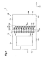
- Fig. 1 is a drawing showing the configuration of the electronic component device according to the present embodiment.
- Fig. 2 is a drawing showing the cross-sectional configuration of the electronic component device according to the present embodiment.
- the electronic component device 1 has a first electronic component 10, a second electronic component 20, first bonding wires W1, and second bonding wires W2, as shown in Figs. 1 and 2 .
- the first electronic component 10 is a solid-state imaging device and the second electronic component 20 a wiring board.
- the first electronic component 10 is a multi-port solid-state imaging device.
- an imaging area to generate an electric charge according to an amount of incident light is divided into a plurality of imaging segments and output portions are disposed for the respective divided imaging segments. Electric charges generated in the divided imaging segments are read out and then output by the corresponding output portions.
- the multi-port solid-state imaging device is described, for example, in Japanese Patent Application Laid-open Publication No. 2002-170947 , Japanese Patent Application Laid-open Publication No. H06-165039 (Japanese Patent No. 3241828 ), and so on and is known in the pertinent technical fields. For this reason, further detailed description is omitted herein about the multi-port solid-state imaging device.
- the first electronic component 10 has a rectangular shape on the plan view thereof and has four sides 10a to 10d constituting the edges of the first electronic component 10.
- the first electronic component 10 includes a pair of principal surfaces 11a, 11b.
- the first electronic component 10 has a photosensitive area (imaging area) 13 disposed on the principal surface 11a side.
- the principal surface 11a side is defined as a light receiving surface side.
- Fig. 1 is the plan view obtained when the first electronic component 10 is viewed from the light receiving surface (principal surface 11a) side.
- the first electronic component 10 has a plurality of first electrode pads 14.
- the first electrode pads 14 are located on the principal surface 11a and outside the photosensitive area 13.
- the first electrode pads 14 are arranged on a line along one side 10a, in the region outside the photosensitive area 13.
- Each first electrode pad 14 is connected to the corresponding output portion through a wire (not shown).
- the first electrode pads 14 have a rectangular shape. In the present embodiment, there are twelve first electrode pads 14 arranged.
- the second electronic component 20 is a wiring board, such as a ceramic substrate or a flexible printed circuit board (FPC), having wires on the surface or inside thereof.
- the second electronic component 20 has four sides 20a to 20d constituting the edges of the second electronic component 20.
- the second electronic component 20 includes a pair of principal surfaces 21a, 21b opposed to each other.
- the second electronic component 20 has a plurality of second electrode pads (twelve second electrode pads in the present embodiment) 24.
- One side 20a of the second electronic component 20 is opposed to the one side 10a of the first electronic component 10.
- the second electrode pads 24 are arranged on a line along the one side 20a on the principal surface 21a of the second electronic component 20.
- a wire (not shown) is connected to each second electrode pad 24.
- Each of the second electrode pads 24 has a first pad portion 24a, a second pad portion 24b, and a third pad portion 24c.
- the third pad portion 24c couples the first pad portion 24a and the second pad portion 24b to each other.
- Each second electrode pad 24 is arranged with an arrangement distance d1 to another in a direction D2 perpendicular to an extending direction D1 of the first bonding wire W1.
- Each first bonding wire W1 is connected to the corresponding first electrode pad 14 and second electrode pad 24. One end of each first bonding wire W1 is connected to the first electrode pad 14 while the other end of each first bonding wire W1 is connected to the first pad portion 24a. Each first bonding wire W1 is disposed so as to extend in the direction D1.
- the extending direction D1 of the first bonding wire W1 intersects with the one side 10a of the first electronic component 10 and with the one side 20a of the second electronic component 20. In the present embodiment, the extending direction D1 of the first bonding wire W1 is approximately perpendicular to each of the sides 10a, 20a.
- the connection between the one end of the first bonding wire W1 and the first electrode pad 14 is implemented by ball bonding.
- the one end of the first bonding wire W1 is melted to form a wire ball at the one end.
- the wire ball is pressed against the first electrode pad 14. It results in ball-bonding the one end of the first bonding wire W1 to the first electrode pad 14.
- connection between the other end of the first bonding wire W1 and the first pad portion 24a is implemented by stitch bonding.
- the other end of the first bonding wire W1 is pressed against the first pad portion 24a by the edge part of the leading end of the capillary and then heat or ultrasonic is applied thereto to connect the first bonding wire W1 to the first pad portion 24a.
- the first bonding wire W1 is cut (or stitched). It results in stitch-bonding the other end of the first bonding wire W1 to the first pad portion 24a.
- Each second bonding wire W2 is connected to the second electrode pad 24.
- One end of the second bonding wire W2 is connected to a connection portion C1 to the first bonding wire W1 on the first pad portion 24a and the other end of the second bonding wire W2 is connected to the second pad portion 24b.
- connection between the one end of the second bonding wire W2 and the first pad portion 24a is implemented by ball bonding.
- the one end of the second bonding wire W2 is melted to form a wire ball at the one end.
- the wire ball is pressed against the connection portion C1. It results in ball-bonding the one end of the second bonding wire W2 to the first pad portion 24a.
- connection between the other end of the second bonding wire W2 and the second pad portion 24b is implemented by stitch bonding.
- the other end of the second bonding wire W2 is pressed against the second pad portion 24b by the edge part of the leading end of the capillary and then heat or ultrasonic is applied thereto to connect the second bonding wire W2 to the second pad portion 24b.
- the second bonding wire W2 is cut (or stitched). It results in stitch-bonding the other end of the second bonding wire W2 to the second pad portion 24b.
- each second bonding wire W2 is disposed so as to extend in the direction intersecting with the extending direction D1 of the first bonding wire W1.
- the first bonding wires W1 and second bonding wires W2 are comprised of a metal material such as gold or copper.
- the present embodiment is so configured that in each second electrode pad 24 the first pad portion 24a is located nearer to the one side 20a than the second pad portion 24b is.
- Each second electrode pad 24 is so disposed that the first pad portion 24a and second pad portion 24b are laid along the direction intersecting at a predetermined first angle to the extending direction D1 of the first bonding wire W1.
- the third pad portion 24c extends in the direction intersecting at the first angle to the extending direction D1 of the first bonding wire W1.
- the first pad portion 24a, the third pad portion 24c, and the second pad portion 24b are located in the order of the first pad portion 24a, the third pad portion 24c, and the second pad portion 24b from the side near to the one side 20a so as to be laid along the direction intersecting at the first angle to the extending direction D1 of the first bonding wire W1.
- the second electrode pad 24 has a parallelogram shape with one side forming a part of the one side 20a and extends along the extending direction of the second bonding wire W2.
- the first electrode pads 14 and the second electrode pads 24 are made of an electroconductive material such as metal by a method such as printing or sputtering. In the present embodiment, the foregoing first angle is set approximately to 135°.
- the arrangement distance of the first electrode pads 14 and the arrangement distance d1 of the second electrode pads 24 are set approximately equal.
- the corresponding first electrode pad 14 and first pad portion 24a of the second electrode pad 24 are opposed to each other in the direction approximately perpendicular to each of the sides 10a, 20a.
- the lengths of the respective first bonding wires W1 connecting the corresponding first electrode pads 14 and first pad portions 24a are approximately equal to each other.
- first electrode pads 14 and first pad portions 24a are electrically connected in a one-to-one relation by the first bonding wires W1.
- a signal output to each first electrode pad 14 is fed through the first bonding wire W1 and the second electrode pad 24 to the wire connected to the second electrode pad 24.
- the first pad portion 24a and the second pad portion 24b in an identical second electrode pad 24 are electrically connected by the third pad portion 24c and the second bonding wire W2.
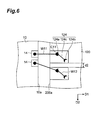
- Fig. 6 is a drawing showing the configuration of the electronic component device disclosed as the comparative example.
- the electronic component device as the comparative example as shown in Fig. 6 , has the first electronic component 10 on which the plurality of first electrode pads 14 are disposed, a second electronic component 120 on which a plurality of second electrode pads 124 are disposed, a plurality of first bonding wires W11, and a plurality of second bonding wires W12.
- Each second electrode pad 124 has a first pad portion 124a, a second pad portion 124b, and a third pad portion 124c.
- the third pad portion 124c couples the first pad portion 124a and the second pad portion 124b to each other.
- Each second electrode pad 124 is arranged with an arrangement distance d2 to another in a direction D2 perpendicular to the extending direction D1 of one first bonding wire W11.
- each first bonding wire W11 is connected to the first electrode pad 14 while the other end of each first bonding wire W11 is connected to the second electrode pad 124.
- One end of each second bonding wire W12 is connected to the first pad portion 124a while the other end of each second bonding wire W12 is connected to the second pad portion 124b.
- a connection C11 between the other end of the first bonding wire W11 and the first pad portion 124a is reinforced by the second bonding wire W12.
- the second electrode pad 124 is expanded in the extending direction D1 of one first bonding wire W11 and in the direction D2 perpendicular to the direction D1, in order to secure the space for connection of the other end of the second bonding wire W12, in the second electrode pad 124 (second pad portion 124b). For this reason, the area of the second electrode pad 124 becomes significantly larger.
- the area of the second electrode pad 124 When the area of the second electrode pad 124 is significantly larger, it results in increasing the areas of mutually opposed regions in the second electrode pad 124 and in the conductive portion disposed in the second electronic component 120. For this reason, it increases the capacitive component composed of the mutually opposed regions. As a consequence, it causes degradation of noise characteristics and high-frequency characteristics of signals send from the first electronic component 10, so as to affect the characteristics of the electronic component device.
- the present embodiment is configured, as described above, so that the second electrode pad 24 has the first pad portion 24a and the second pad portion 24b laid along the direction intersecting at the predetermined first angle (135° in the present embodiment) to the extending direction D1 of the first bonding wire W1. For this reason, although each second electrode pad 24 has the second pad portion 24b to which the other end of the second bonding wire W2 is connected, the area of each second electrode pad 24 is reduced in the foregoing direction intersecting with the extending direction D1 of the first bonding wire W1.
- each second electrode pad 24 Since the area of each second electrode pad 24 is reduced in the foregoing direction intersecting with the extending direction D1 of the first bonding wire W1, the distance to the other conductive portion is set relatively narrow. Namely, the present embodiment does not have to largely change the arrangement distance d1 of the second electrode pads 24 in the direction D2 perpendicular to the extending direction D1 of the first bonding wire W1, for avoiding the interference between adjacent second electrode pads 24. For this reason, the connection portion C1 between the first bonding wire W1 and the first pad portion 24a can be reinforced, while suppressing the increase in the size of the electronic component device 1.
- the areas of the mutually opposed regions are relatively small in the second electrode pad 24 and in the conductive portion disposed in the second electronic component 120. For this reason, it is feasible to suppress the increase in the capacitive component composed of the mutually opposed regions.
- connection between the other end of the first bonding wire W1 and the first pad portion 24a is implemented by stitch bonding. Namely, without forming a wire ball in the first bonding wire W1, the connection between the other end of the first bonding wire W1 and the first pad portion 24a is made by pressing the other end of the first bonding wire W1 against the first pad portion 24a. For this reason, the connection portion C1 between the other end of the first bonding wire W1 and the first pad portion 24a has the connection strength relatively weak.
- the connection portion C1 between the other end of the first bonding wire W1 and the first pad portion 24a is reinforced by the second bonding wire W2, so as to enhance the connection strength at the connection portion C1, whereby the electronic component device 1 becomes suitable for practical use.
- the first pad portion 24a is located nearer to the side 20a than the second pad portion 24b is. For this reason, the wire bonding to each second electrode pad 24 can be readily implemented in the case where the second electronic component 20 is a ceramic substrate the edges of which are approximately flat on the principal surface 11a and which is made of a relatively hard material.
- the lengths of the respective first bonding wires W1 connecting the corresponding first electrode pads 14 and second electrode pads 24 are approximately equal. For this reason, it is feasible to reduce occurrence of variation in signals sent between the first electrode pads 14 and the second electrode pads 24 connected by the first bonding wires W1.
- Figs. 3 to 5 are drawings showing the configurations of the electronic component devices according to the modification examples of the embodiment.
- the first pad portion 24a is located nearer to the one side 20a than the second pad portion 24b is, but the configuration of the second electrode pad 24 does not have to be limited to it.
- the arrangement of the first pad portion 24a and the second pad portion 24b may be reverse to the arrangement in the second electronic component 20.
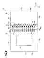
- each second electrode pad 44 disposed on a principal surface 41a of the second electronic component 40 a second pad portion 44b is located nearer to one side 40a than a first pad portion 44a is.
- the second electronic component 40 has four sides 40a to 40d constituting the edges of the second electronic component 40.
- Each second electrode pad 44 has the first pad portion 44a, the second pad portion 44b, and a third pad portion 44c.
- the first pad portion 44a, the second pad portion 44b, and the third pad portion 44c are located in the order of the second pad portion 44b, the third pad portion 44c, and the first pad portion 44a from the one side 40a side.
- a connection portion C2 between the other end of the first bonding wire W1 and the first pad portion 44a is reinforced by the second bonding wire W2.
- the second electronic component 40 is a flexible wiring board.
- the edges thereof can be curved in such a manner that the principal surface 21a with the second electrode pads 24 being arranged thereon is an outside surface of curvature.
- the edges of the flexible wiring board are curved in this manner, it is difficult to implement the wire bonding to the electrode pads disposed at the edge of the principal surface 41a.
- the connection portion C2 between the other end of the first bonding wire W1 and the first pad portion 44a is located relatively apart from the edge of the principal surface 41 a. It can further enhance the connection strength at the connection portion C2 between the other end of the first bonding wire W1 and the first pad portion 44a.
- the capillary generally has the leading end with a cross section of a V-tapered shape.
- the edges of the flexible wiring board are curved as described above.
- each second electrode pad 64 may have a portion extending along the extending direction D1 of the first bonding wire W1, at a position nearer to one side 60a with respect to a first pad portion 64a.
- the second electronic component 60 has four sides 60a to 60d constituting the edges of the second electronic component 60.
- Each second electrode pad 64 disposed on the principal surface 61a of the second electronic component 60 has the first pad portion 64a, a second pad portion 64b, and a third pad portion 64c.
- the first pad portion 64a, the second pad portion 64b, and the third pad portion 64c are located in the order of the first pad portion 64a, third pad portion 64c, and second pad portion 64b from the one side 60a side.
- a connection portion C3 between the other end of the first bonding wire W1 and the first pad portion 64a is reinforced by the second bonding wire W2.
- the second electronic component 80 in the electronic component device 4 may have a plurality of second electrode pads 84 and a plurality of second electrode pads 85 disposed in respective directions different from each other.
- the second electrode pads 84 and the second electrode pads 85 are disposed on a principal surface 81a of the second electronic component 80.
- the second electronic component 80 has four sides 80a to 80d constituting the edges of the second electronic component 80.
- Each second electrode pad 84 has a first pad portion 84a, a second pad portion 84b, and a third pad portion 84c.
- the first pad portion 84a, the second pad portion 84b, and the third pad portion 84c are located in the order of the first pad portion 84a, the third pad portion 84c, and the second pad portion 84b from the one side 80a side.
- the plurality of second electrode pads 84 are disposed in parallel to each other.
- the first pad portion 84a, third pad portion 84c, and second pad portion 84b are arranged along a first direction intersecting with the extending direction D1 of the first bonding wire W1.
- Each second electrode pad 85 has a first pad portion 85a, a second pad portion 85b, and a third pad portion 85c.
- the first pad portion 85a, the second pad portion 85b, and the third pad portion 85c are located in the order of the first pad portion 85a, the third pad portion 85c, and the second pad portion 85b from the one side 80a side.
- the plurality of second electrode pads 85 are disposed in parallel to each other.
- the first pad portion 85a, third pad portion 85c, and second pad portion 85b are arranged along a second direction intersecting with the extending direction D1 of the first bonding wire W1 and with the foregoing first direction.
- the wires connected to the respective second electrode pads 84 and the wires connected to the respective second electrode pads 85 can be disposed separately in two regions on the principal surface 81 a of the second electronic component 80. It can enhance degrees of freedom for routing of wiring patterns in the second electronic component 80.
- a connection portion C4 between the other end of the first bonding wire W2 and each first pad portion 84a or 85a is reinforced by the second bonding wire W2.
- connection between the one end of the first bonding wire W1 and the first electrode pad 14 is implemented by ball bonding and the connection between the other end of the first bonding wire W1 and the first pad portion 24a, 44a, 64a, 84a, or 85a is implemented by stitch bonding.
- the connection between the one end of the second bonding wire W2 and the first pad portion 24a, 44a, 64a, 84a, or 85a is implemented by ball bonding and the connection between the other end of the second bonding wire W2 and the second pad portion 24b, 44b, 64b, 84b, or 85b is implemented by stitch bonding.
- these connections do not have to be limited to the above-described bonding methods.
- the numbers of the first and second electrode pads 14, 24, 44, 64, 84, 85 do not have to be limited to those disclosed in the foregoing embodiment and modification examples.
- the first and second electrode pads 14, 24, 44, 64, 84, or 85 do not have to be disposed on a line, but may be disposed in a zigzag pattern.
- the present invention is applicable to the electronic component apparatus having the solid-state imaging device and the wiring board to which the solid-state imaging device is connected.
- first electronic component devices 10 first electronic component; 11a, 11b principal surfaces; 20a-20d, 40a-40d, 60a-60d, 80a-80d sides; 13 photosensitive area; 14 first electrode pads; 20, 40, 60, 80 second electronic components; 21a, 21b, 41a, 61a, 81a principal surfaces; 24, 44, 64, 84, 85 second electrode pads; 24a, 44a, 64a, 84a, 85a first pad portions; 24b, 44b, 64b, 84b, 85b second pad portions; 24c, 44c, 64c, 84c, 85c third pad portions; C1-C4 connection portions between first pad portions and first bonding wires; D1 extending direction of first bonding wires; W1 first bonding wires; W2 second bonding wires.
Landscapes
- Wire Bonding (AREA)
- Physics & Mathematics (AREA)
- Geometry (AREA)
- Solid State Image Pick-Up Elements (AREA)
Abstract
Description
- The present invention relates to an electronic component device.
- There is a known electronic component device having a first electronic component on which a first electrode pad is disposed, a second electronic component on which a second electrode pad is disposed, and a bonding wire having one end connected to the first electrode pad and the other end connected to the second electrode pad (e.g., cf. Patent Literature 1).
- Patent Literature 1: Japanese Patent Application Laid-open Publication No.
2011-101051 - It is conceivable to reinforce a connection portion between the other end of each bonding wire (which will be referred to hereinafter as "first bonding wire") and the second electrode pad by another bonding wire (which will be referred to hereinafter as "second bonding wire") different from the first bonding wire. In this case, one end of the second bonding wire is connected to the foregoing connection portion and the other end of the second bonding wire is connected to the second electrode pad, for example, at a position different from the connection portion.
- In implementing the wire bonding between the first electrode pad and the second electrode pad, a leading end of a bonding wire fed out of a capillary is first connected to the first electrode pad. Thereafter, the capillary is moved to the position of the second electrode pad and then the other end of the bonding wire is connected to the second electrode pad. A loop is formed in a predetermined shape in the bonding wire, so as to prevent the bonding wire connected to the first electrode pad and the second electrode pad from coming into contact with the first electronic component and the second electronic component. For forming the loop of the predetermined shape in the bonding wire, the one end of the bonding wire fed out of the capillary is connected to the first electrode pad and thereafter the capillary is once moved in a direction opposite to a direction from the first electrode pad to the second electrode pad.
- In the case where the connection portion between the other end of the first bonding wire and the second electrode pad is reinforced by the second bonding wire, if a connection portion of the other end of the second bonding wire is located on an extension of the first bonding wire, the following problem will arise. For forming the aforementioned loop in the second bonding wire, the one end of the second bonding wire is connected to the connection portion and thereafter the capillary is moved in the direction opposite to the direction in which the connection portion of the other end of the second bonding wire is located. At this time, the capillary may come into contact with the first wire bonding. In order to prevent the capillary from coming into contact with the first bonding wire, the second bonding wire needs to be connected to the second electrode pad so as not to locate the connection portion of the other end of the second bonding wire on the extension of the first bonding wire.
- For not locating the connection portion of the other end of the second bonding wire on the extension of the first bonding wire, it is necessary to increase the area of the second electrode pad so as to secure a space for connection of the second bonding wire. However, the increase in the area of the second electrode pad may cause interference of the second electrode pad with another conductive portion (e.g., an electrode pad or the like) located around the second electrode pad. For avoiding the interference of the second electrode pad with the other conductive portion, the arrangement distance (pitch) of the second electrode pad and the other conductive portion has to be changed. As a consequence, the size of the electronic component becomes larger.
- The present invention has been accomplished in view of the above-described circumstances and it is an object of the present invention to provide an electronic component device allowing the connection portion between the bonding wire and electrode pad to be reinforced, while suppressing the increase in the size of the electronic component.
- One aspect of the present invention is an electronic component device includes a first electronic component on which a first electrode pad is disposed, a second electronic component on which a second electrode pad having a first pad portion and a second pad portion is disposed, a first bonding wire having one end connected to the first electrode pad and the other end connected to the first pad portion, and a second bonding wire having one end connected to a connection portion between the first pad portion and the first bonding wire and the other end connected to the second pad portion. The second electrode pad is disposed on the second electronic component so that the first pad portion and the second pad portion are laid along a direction intersecting with an extending direction of the first bonding wire. The extending direction of the first bonding wire intersects with an extending direction of the second bonding wire.
- In the present invention, the first pad portion and second pad portion of the second electrode pad are laid along the direction intersecting with the extending direction of the first bonding wire. This arrangement reduces the area of the second electrode pad in the direction intersecting with the extending direction of the first bonding wire, while the second electrode pad has the second pad portion connected to the other end of the second bonding wire. When the area of the second electrode pad is reduced, the arrangement distance to the other conductive portion is set relatively narrow. Namely, there is no need for largely changing the arrangement distance to the other conductive portion, in order to avoid the interference with the other conductive portion located around the second electrode pad. As a result, it is feasible to reinforce the connection portion between the bonding wire and the electrode pad, while suppressing the increase in the size of the electronic component.
- The second electrode pad may further have a third pad portion coupling the first pad portion and the second pad portion to each other, and the third pad portion may extend along the direction intersecting with the extending direction of the first bonding wire. In this case, the areas of the first pad portion and the second pad portion are set relatively wide and thus it becomes easier to implement wire connections to the respective pad portions.
- The first electronic component may be a solid-state imaging device which has one principal surface and which has a plurality of first electrode pads arranged along one side of the one principal surface. The second electronic component may have an edge opposed to the one side and have a plurality of second electrode pads arranged along the edge. The electronic component device may include a plurality of first bonding wires each of which connects the corresponding first electrode pad and first pad portion of the second electrode pad and a plurality of second bonding wires each of which connects the corresponding first pad portion and second pad portion. In this case, though each second electrode pad has the second pad portion to which the other end of the second bonding wire is connected, the area of each second electrode pad is reduced in the direction intersecting with the extending direction of the first bonding wire.
- In each second electrode pad, the first pad portion may be located nearer to the edge than the second pad portion is.
- In each second electrode pad, the second pad portion may be located nearer to the edge than the first pad portion is.
- The plurality of second electrode pads may include: a plurality of second electrode pads each of which is disposed so that the first pad portion and the second pad portion are laid along a first direction intersecting with the extending direction of the first bonding wire and which are disposed in parallel to each other; and a plurality of second electrode pads each of which is disposed so that the first pad portion and the second pad portion are laid along a second direction intersecting with the extending direction of the first bonding wire and with the first direction and which are disposed in parallel to each other.
- The second electronic component may be a flexible wiring board.
- The present invention has provided the electronic component device allowing the connection portion between the bonding wire and electrode pad to be reinforced, while suppressing the increase in the size of the electronic component.
-
-
Fig. 1 is a drawing showing a configuration of an electronic component device according to an embodiment of the present invention. -
Fig. 2 is a drawing for explaining a cross-sectional configuration of the electronic component device according to the embodiment. -
Fig. 3 is a drawing showing a configuration of an electronic component device according to a modification example of the embodiment. -
Fig. 4 is a drawing showing a configuration of an electronic component device according to another modification example of the embodiment. -
Fig. 5 is a drawing showing a configuration of an electronic component device according to another modification example of the embodiment. -
Fig. 6 is a drawing showing a configuration of an electronic component device disclosed as a comparative example. - Preferred embodiments of the present invention will be described below in detail with reference to the accompanying drawings. Identical elements or elements with identical functionality will be denoted by the same reference signs in the description, without redundant description.
- First, the configuration of the electronic component device 1 according to the embodiment of the invention will be described with reference to
Fig. 1 andFig. 2 .Fig. 1 is a drawing showing the configuration of the electronic component device according to the present embodiment.Fig. 2 is a drawing showing the cross-sectional configuration of the electronic component device according to the present embodiment. The electronic component device 1 has a firstelectronic component 10, a secondelectronic component 20, first bonding wires W1, and second bonding wires W2, as shown inFigs. 1 and2 . In the present embodiment, the firstelectronic component 10 is a solid-state imaging device and the secondelectronic component 20 a wiring board. - The first
electronic component 10 is a multi-port solid-state imaging device. In the multi-port solid-state imaging device, an imaging area to generate an electric charge according to an amount of incident light is divided into a plurality of imaging segments and output portions are disposed for the respective divided imaging segments. Electric charges generated in the divided imaging segments are read out and then output by the corresponding output portions. The multi-port solid-state imaging device is described, for example, in Japanese Patent Application Laid-open Publication No.2002-170947 H06-165039 3241828 - The first
electronic component 10 has a rectangular shape on the plan view thereof and has foursides 10a to 10d constituting the edges of the firstelectronic component 10. The firstelectronic component 10 includes a pair ofprincipal surfaces electronic component 10 has a photosensitive area (imaging area) 13 disposed on theprincipal surface 11a side. In the firstelectronic component 10, theprincipal surface 11a side is defined as a light receiving surface side.Fig. 1 is the plan view obtained when the firstelectronic component 10 is viewed from the light receiving surface (principal surface 11a) side. - The first
electronic component 10 has a plurality offirst electrode pads 14. Thefirst electrode pads 14 are located on theprincipal surface 11a and outside thephotosensitive area 13. Thefirst electrode pads 14 are arranged on a line along oneside 10a, in the region outside thephotosensitive area 13. Eachfirst electrode pad 14 is connected to the corresponding output portion through a wire (not shown). Thefirst electrode pads 14 have a rectangular shape. In the present embodiment, there are twelvefirst electrode pads 14 arranged. - The second
electronic component 20 is a wiring board, such as a ceramic substrate or a flexible printed circuit board (FPC), having wires on the surface or inside thereof. The secondelectronic component 20 has foursides 20a to 20d constituting the edges of the secondelectronic component 20. The secondelectronic component 20 includes a pair ofprincipal surfaces electronic component 20 has a plurality of second electrode pads (twelve second electrode pads in the present embodiment) 24. Oneside 20a of the secondelectronic component 20 is opposed to the oneside 10a of the firstelectronic component 10. Thesecond electrode pads 24 are arranged on a line along the oneside 20a on theprincipal surface 21a of the secondelectronic component 20. A wire (not shown) is connected to eachsecond electrode pad 24. Each of thesecond electrode pads 24 has afirst pad portion 24a, asecond pad portion 24b, and athird pad portion 24c. Thethird pad portion 24c couples thefirst pad portion 24a and thesecond pad portion 24b to each other. Eachsecond electrode pad 24 is arranged with an arrangement distance d1 to another in a direction D2 perpendicular to an extending direction D1 of the first bonding wire W1. - Each first bonding wire W1 is connected to the corresponding
first electrode pad 14 andsecond electrode pad 24. One end of each first bonding wire W1 is connected to thefirst electrode pad 14 while the other end of each first bonding wire W1 is connected to thefirst pad portion 24a. Each first bonding wire W1 is disposed so as to extend in the direction D1. The extending direction D1 of the first bonding wire W1 intersects with the oneside 10a of the firstelectronic component 10 and with the oneside 20a of the secondelectronic component 20. In the present embodiment, the extending direction D1 of the first bonding wire W1 is approximately perpendicular to each of thesides - The connection between the one end of the first bonding wire W1 and the
first electrode pad 14 is implemented by ball bonding. First, the one end of the first bonding wire W1 is melted to form a wire ball at the one end. Thereafter, under application of heat or ultrasonic, the wire ball is pressed against thefirst electrode pad 14. It results in ball-bonding the one end of the first bonding wire W1 to thefirst electrode pad 14. - The connection between the other end of the first bonding wire W1 and the
first pad portion 24a is implemented by stitch bonding. First, the other end of the first bonding wire W1 is pressed against thefirst pad portion 24a by the edge part of the leading end of the capillary and then heat or ultrasonic is applied thereto to connect the first bonding wire W1 to thefirst pad portion 24a. Thereafter, the first bonding wire W1 is cut (or stitched). It results in stitch-bonding the other end of the first bonding wire W1 to thefirst pad portion 24a. - Each second bonding wire W2 is connected to the
second electrode pad 24. One end of the second bonding wire W2 is connected to a connection portion C1 to the first bonding wire W1 on thefirst pad portion 24a and the other end of the second bonding wire W2 is connected to thesecond pad portion 24b. - The connection between the one end of the second bonding wire W2 and the
first pad portion 24a is implemented by ball bonding. First, the one end of the second bonding wire W2 is melted to form a wire ball at the one end. Thereafter, under application of heat or ultrasonic, the wire ball is pressed against the connection portion C1. It results in ball-bonding the one end of the second bonding wire W2 to thefirst pad portion 24a. - The connection between the other end of the second bonding wire W2 and the
second pad portion 24b is implemented by stitch bonding. First, the other end of the second bonding wire W2 is pressed against thesecond pad portion 24b by the edge part of the leading end of the capillary and then heat or ultrasonic is applied thereto to connect the second bonding wire W2 to thesecond pad portion 24b. Thereafter, the second bonding wire W2 is cut (or stitched). It results in stitch-bonding the other end of the second bonding wire W2 to thesecond pad portion 24b. - The extending direction of the second bonding wire W2 intersects with the extending direction D1 of the first bonding wire W1. Namely, each second bonding wire W2 is disposed so as to extend in the direction intersecting with the extending direction D1 of the first bonding wire W1. The first bonding wires W1 and second bonding wires W2 are comprised of a metal material such as gold or copper.
- The present embodiment is so configured that in each
second electrode pad 24 thefirst pad portion 24a is located nearer to the oneside 20a than thesecond pad portion 24b is. Eachsecond electrode pad 24 is so disposed that thefirst pad portion 24a andsecond pad portion 24b are laid along the direction intersecting at a predetermined first angle to the extending direction D1 of the first bonding wire W1. Thethird pad portion 24c extends in the direction intersecting at the first angle to the extending direction D1 of the first bonding wire W1. Namely, in thesecond electrode pad 24, thefirst pad portion 24a, thethird pad portion 24c, and thesecond pad portion 24b are located in the order of thefirst pad portion 24a, thethird pad portion 24c, and thesecond pad portion 24b from the side near to the oneside 20a so as to be laid along the direction intersecting at the first angle to the extending direction D1 of the first bonding wire W1. Thesecond electrode pad 24 has a parallelogram shape with one side forming a part of the oneside 20a and extends along the extending direction of the second bonding wire W2. Thefirst electrode pads 14 and thesecond electrode pads 24 are made of an electroconductive material such as metal by a method such as printing or sputtering. In the present embodiment, the foregoing first angle is set approximately to 135°. - In the present embodiment, the arrangement distance of the
first electrode pads 14 and the arrangement distance d1 of thesecond electrode pads 24 are set approximately equal. The correspondingfirst electrode pad 14 andfirst pad portion 24a of thesecond electrode pad 24 are opposed to each other in the direction approximately perpendicular to each of thesides first electrode pads 14 andfirst pad portions 24a are approximately equal to each other. - In the present embodiment, the corresponding
first electrode pads 14 andfirst pad portions 24a are electrically connected in a one-to-one relation by the first bonding wires W1. A signal output to eachfirst electrode pad 14 is fed through the first bonding wire W1 and thesecond electrode pad 24 to the wire connected to thesecond electrode pad 24. Thefirst pad portion 24a and thesecond pad portion 24b in an identicalsecond electrode pad 24 are electrically connected by thethird pad portion 24c and the second bonding wire W2. - The below will describe the electronic component device disclosed as a comparative example.
Fig. 6 is a drawing showing the configuration of the electronic component device disclosed as the comparative example. The electronic component device as the comparative example, as shown inFig. 6 , has the firstelectronic component 10 on which the plurality offirst electrode pads 14 are disposed, a secondelectronic component 120 on which a plurality ofsecond electrode pads 124 are disposed, a plurality of first bonding wires W11, and a plurality of second bonding wires W12. - Each
second electrode pad 124 has afirst pad portion 124a, asecond pad portion 124b, and athird pad portion 124c. Thethird pad portion 124c couples thefirst pad portion 124a and thesecond pad portion 124b to each other. Eachsecond electrode pad 124 is arranged with an arrangement distance d2 to another in a direction D2 perpendicular to the extending direction D1 of one first bonding wire W11. - One end of each first bonding wire W11 is connected to the
first electrode pad 14 while the other end of each first bonding wire W11 is connected to thesecond electrode pad 124. One end of each second bonding wire W12 is connected to thefirst pad portion 124a while the other end of each second bonding wire W12 is connected to thesecond pad portion 124b. A connection C11 between the other end of the first bonding wire W11 and thefirst pad portion 124a is reinforced by the second bonding wire W12. In the electronic component device as the comparative example, thesecond electrode pad 124 is expanded in the extending direction D1 of one first bonding wire W11 and in the direction D2 perpendicular to the direction D1, in order to secure the space for connection of the other end of the second bonding wire W12, in the second electrode pad 124 (second pad portion 124b). For this reason, the area of thesecond electrode pad 124 becomes significantly larger. - When the area of the
second electrode pad 124 is significantly larger, it results in increasing the areas of mutually opposed regions in thesecond electrode pad 124 and in the conductive portion disposed in the secondelectronic component 120. For this reason, it increases the capacitive component composed of the mutually opposed regions. As a consequence, it causes degradation of noise characteristics and high-frequency characteristics of signals send from the firstelectronic component 10, so as to affect the characteristics of the electronic component device. - When the area of the
second electrode pad 124 is expanded in the direction D2 perpendicular to the extending direction D1 of one first bonding wire W11 as in the electronic component device shown inFig. 6 , it becomes necessary to set the arrangement distance d2 smaller. For this reason, a short circuit is likely to occur between adjacentsecond electrode pads 124. It is conceivable to widen the arrangement distance d2 of thesecond electrode pads 124, in order to prevent the short circuit from occurring between adjacentsecond electrode pads 124. In this case, the size of the secondelectronic component 120 becomes unnecessarily larger. - In contrast to it, the present embodiment is configured, as described above, so that the
second electrode pad 24 has thefirst pad portion 24a and thesecond pad portion 24b laid along the direction intersecting at the predetermined first angle (135° in the present embodiment) to the extending direction D1 of the first bonding wire W1. For this reason, although eachsecond electrode pad 24 has thesecond pad portion 24b to which the other end of the second bonding wire W2 is connected, the area of eachsecond electrode pad 24 is reduced in the foregoing direction intersecting with the extending direction D1 of the first bonding wire W1. - Since the area of each
second electrode pad 24 is reduced in the foregoing direction intersecting with the extending direction D1 of the first bonding wire W1, the distance to the other conductive portion is set relatively narrow. Namely, the present embodiment does not have to largely change the arrangement distance d1 of thesecond electrode pads 24 in the direction D2 perpendicular to the extending direction D1 of the first bonding wire W1, for avoiding the interference between adjacentsecond electrode pads 24. For this reason, the connection portion C1 between the first bonding wire W1 and thefirst pad portion 24a can be reinforced, while suppressing the increase in the size of the electronic component device 1. - Since the area of the
second electrode pad 24 is reduced as described above, the areas of the mutually opposed regions are relatively small in thesecond electrode pad 24 and in the conductive portion disposed in the secondelectronic component 120. For this reason, it is feasible to suppress the increase in the capacitive component composed of the mutually opposed regions. - When the area of the
second electrode pad 24 is reduced in the foregoing direction intersecting with the extending direction D1 of the first bonding wire W1, there is no reduction in the arrangement distance d1 of thesecond electrode pads 24 in the direction D2 perpendicular to the extending direction D1 of the first bonding wire W1. For this reason, it is also feasible to prevent a short circuit from occurring between adjacentsecond electrode pads 24. - The connection between the other end of the first bonding wire W1 and the
first pad portion 24a is implemented by stitch bonding. Namely, without forming a wire ball in the first bonding wire W1, the connection between the other end of the first bonding wire W1 and thefirst pad portion 24a is made by pressing the other end of the first bonding wire W1 against thefirst pad portion 24a. For this reason, the connection portion C1 between the other end of the first bonding wire W1 and thefirst pad portion 24a has the connection strength relatively weak. The connection portion C1 between the other end of the first bonding wire W1 and thefirst pad portion 24a is reinforced by the second bonding wire W2, so as to enhance the connection strength at the connection portion C1, whereby the electronic component device 1 becomes suitable for practical use. - In the
second electrode pad 24, thefirst pad portion 24a is located nearer to theside 20a than thesecond pad portion 24b is. For this reason, the wire bonding to eachsecond electrode pad 24 can be readily implemented in the case where the secondelectronic component 20 is a ceramic substrate the edges of which are approximately flat on theprincipal surface 11a and which is made of a relatively hard material. - The lengths of the respective first bonding wires W1 connecting the corresponding
first electrode pads 14 andsecond electrode pads 24 are approximately equal. For this reason, it is feasible to reduce occurrence of variation in signals sent between thefirst electrode pads 14 and thesecond electrode pads 24 connected by the first bonding wires W1. - The preferred embodiment of the present invention was described above and it should be noted that the present invention is not always limited to the above-described embodiment but can be modified in many ways without departing from the spirit and scope of the invention.
- The configurations of electronic component devices 2 to 4 according to modification examples of the embodiment will be described with reference to
Figs. 3 to 5. Figs. 3 to 5 are drawings showing the configurations of the electronic component devices according to the modification examples of the embodiment. In thesecond electrode pad 24, thefirst pad portion 24a is located nearer to the oneside 20a than thesecond pad portion 24b is, but the configuration of thesecond electrode pad 24 does not have to be limited to it. Like the secondelectronic component 40 in the electronic component device 2 shown inFig. 3 , the arrangement of thefirst pad portion 24a and thesecond pad portion 24b may be reverse to the arrangement in the secondelectronic component 20. Namely, in eachsecond electrode pad 44 disposed on aprincipal surface 41a of the secondelectronic component 40, asecond pad portion 44b is located nearer to oneside 40a than afirst pad portion 44a is. The secondelectronic component 40 has foursides 40a to 40d constituting the edges of the secondelectronic component 40. Eachsecond electrode pad 44 has thefirst pad portion 44a, thesecond pad portion 44b, and athird pad portion 44c. Thefirst pad portion 44a, thesecond pad portion 44b, and thethird pad portion 44c are located in the order of thesecond pad portion 44b, thethird pad portion 44c, and thefirst pad portion 44a from the oneside 40a side. A connection portion C2 between the other end of the first bonding wire W1 and thefirst pad portion 44a is reinforced by the second bonding wire W2. - The second
electronic component 40 is a flexible wiring board. When the flexible wiring board is cut into a product size, the edges thereof can be curved in such a manner that theprincipal surface 21a with thesecond electrode pads 24 being arranged thereon is an outside surface of curvature. When the edges of the flexible wiring board are curved in this manner, it is difficult to implement the wire bonding to the electrode pads disposed at the edge of theprincipal surface 41a. When thesecond pad portion 44b is located nearer to the oneside 40a than thefirst pad portion 44a is located in thesecond electrode pad 44, as shown inFig. 3 , the connection portion C2 between the other end of the first bonding wire W1 and thefirst pad portion 44a is located relatively apart from the edge of theprincipal surface 41 a. It can further enhance the connection strength at the connection portion C2 between the other end of the first bonding wire W1 and thefirst pad portion 44a. - The capillary generally has the leading end with a cross section of a V-tapered shape. The edges of the flexible wiring board are curved as described above. For these reasons, when the capillary is moved from the vicinity of the
first pad portion 44a toward thesecond pad portion 44b, the other end of the second bonding wire W2 can be pressed against thesecond pad portion 44b in a state in which the tapered surface of the leading end of the capillary is kept approximately parallel to the edge of theprincipal surface 41a of the secondelectronic component 40. Therefore, it is feasible to enhance the connection strength between the other end of the second bonding wire W2 and thesecond pad portion 44b. - In the second
electronic component 20, thesecond electrode pads 24 have the parallelogram shape, but the shape thereof does not have to be limited to the parallelogram. Like the secondelectronic component 60 in the electronic component device 3 shown inFig. 4 , eachsecond electrode pad 64 may have a portion extending along the extending direction D1 of the first bonding wire W1, at a position nearer to oneside 60a with respect to afirst pad portion 64a. The secondelectronic component 60 has foursides 60a to 60d constituting the edges of the secondelectronic component 60. Eachsecond electrode pad 64 disposed on theprincipal surface 61a of the secondelectronic component 60 has thefirst pad portion 64a, asecond pad portion 64b, and athird pad portion 64c. Thefirst pad portion 64a, thesecond pad portion 64b, and thethird pad portion 64c are located in the order of thefirst pad portion 64a,third pad portion 64c, andsecond pad portion 64b from the oneside 60a side. A connection portion C3 between the other end of the first bonding wire W1 and thefirst pad portion 64a is reinforced by the second bonding wire W2. - In the second
electronic component 20, all thesecond electrode pads 24 are laid along the same direction but they do not have to be limited to this arrangement. As shown inFig. 5 , the secondelectronic component 80 in the electronic component device 4 may have a plurality ofsecond electrode pads 84 and a plurality ofsecond electrode pads 85 disposed in respective directions different from each other. Thesecond electrode pads 84 and thesecond electrode pads 85 are disposed on aprincipal surface 81a of the secondelectronic component 80. The secondelectronic component 80 has foursides 80a to 80d constituting the edges of the secondelectronic component 80. - Each
second electrode pad 84 has afirst pad portion 84a, asecond pad portion 84b, and athird pad portion 84c. Thefirst pad portion 84a, thesecond pad portion 84b, and thethird pad portion 84c are located in the order of thefirst pad portion 84a, thethird pad portion 84c, and thesecond pad portion 84b from the oneside 80a side. The plurality ofsecond electrode pads 84 are disposed in parallel to each other. In eachsecond electrode pad 84, thefirst pad portion 84a,third pad portion 84c, andsecond pad portion 84b are arranged along a first direction intersecting with the extending direction D1 of the first bonding wire W1. Eachsecond electrode pad 85 has afirst pad portion 85a, asecond pad portion 85b, and athird pad portion 85c. Thefirst pad portion 85a, thesecond pad portion 85b, and thethird pad portion 85c are located in the order of thefirst pad portion 85a, thethird pad portion 85c, and thesecond pad portion 85b from the oneside 80a side. The plurality ofsecond electrode pads 85 are disposed in parallel to each other. In eachsecond electrode pad 85, thefirst pad portion 85a,third pad portion 85c, andsecond pad portion 85b are arranged along a second direction intersecting with the extending direction D1 of the first bonding wire W1 and with the foregoing first direction. In this case, for example, the wires connected to the respectivesecond electrode pads 84 and the wires connected to the respectivesecond electrode pads 85 can be disposed separately in two regions on theprincipal surface 81 a of the secondelectronic component 80. It can enhance degrees of freedom for routing of wiring patterns in the secondelectronic component 80. A connection portion C4 between the other end of the first bonding wire W2 and eachfirst pad portion - In the above-described embodiment and modification examples, the connection between the one end of the first bonding wire W1 and the
first electrode pad 14 is implemented by ball bonding and the connection between the other end of the first bonding wire W1 and thefirst pad portion first pad portion second pad portion - The numbers of the first and
second electrode pads second electrode pads - The present invention is applicable to the electronic component apparatus having the solid-state imaging device and the wiring board to which the solid-state imaging device is connected.
- 1-4 electronic component devices; 10 first electronic component; 11a, 11b principal surfaces; 20a-20d, 40a-40d, 60a-60d, 80a-80d sides; 13 photosensitive area; 14 first electrode pads; 20, 40, 60, 80 second electronic components; 21a, 21b, 41a, 61a, 81a principal surfaces; 24, 44, 64, 84, 85 second electrode pads; 24a, 44a, 64a, 84a, 85a first pad portions; 24b, 44b, 64b, 84b, 85b second pad portions; 24c, 44c, 64c, 84c, 85c third pad portions; C1-C4 connection portions between first pad portions and first bonding wires; D1 extending direction of first bonding wires; W1 first bonding wires; W2 second bonding wires.
Claims (7)
- An electronic component device comprising:a first electronic component on which a first electrode pad is disposed;a second electronic component on which a second electrode pad having a first pad portion and a second pad portion is disposed;a first bonding wire having one end connected to the first electrode pad and the other end connected to the first pad portion; anda second bonding wire having one end connected to a connection portion between the first pad portion and the first bonding wire and the other end connected to the second pad portion,wherein the second electrode pad is disposed on the second electronic component so that the first pad portion and the second pad portion are laid along a direction intersecting with an extending direction of the first bonding wire, andwherein the extending direction of the first bonding wire intersects with an extending direction of the second bonding wire.
- The electronic component device according to claim 1,
wherein the second electrode pad further has a third pad portion coupling the first pad portion and the second pad portion to each other, and
wherein the third pad portion extends along the direction intersecting with the extending direction of the first bonding wire. - The electronic component device according to claim 1 or 2,
wherein the first electronic component is a solid-state imaging device which has one principal surface and which has a plurality of said first electrode pads arranged along one side of the one principal surface,
wherein the second electronic component has an edge opposed to the one side and has a plurality of said second electrode pads arranged along the edge, and
wherein the electronic component device comprises:a plurality of said first bonding wires each of which connects the corresponding first electrode pad and first pad portion of the second electrode pad; anda plurality of said second bonding wires each of which connects the corresponding first pad portion and second pad portion. - The electronic component device according to claim 3,
wherein in each said second electrode pad, the first pad portion is located nearer to the edge than the second pad portion is. - The electronic component device according to claim 3,
wherein in each said second electrode pad, the second pad portion is located nearer to the edge than the first pad portion is. - The electronic component device according to claim 3,
wherein the plurality of second electrode pads include:a plurality of said second electrode pads each of which is disposed so that the first pad portion and the second pad portion are laid along a first direction intersecting with the extending direction of the first bonding wire and which are disposed in parallel to each other; anda plurality of said second electrode pads each of which is disposed so that the first pad portion and the second pad portion are laid along a second direction intersecting with the extending direction of the first bonding wire and with the first direction and which are disposed in parallel to each other. - The electronic component device according to any one of claims 1 to 6,
wherein the second electronic component is a flexible wiring board.
Applications Claiming Priority (2)
| Application Number | Priority Date | Filing Date | Title |
|---|---|---|---|
| JP2013007579 | 2013-01-18 | ||
| PCT/JP2013/075706 WO2014112158A1 (en) | 2013-01-18 | 2013-09-24 | Electronic component device |
Publications (3)
| Publication Number | Publication Date |
|---|---|
| EP2947684A1 true EP2947684A1 (en) | 2015-11-25 |
| EP2947684A4 EP2947684A4 (en) | 2016-10-05 |
| EP2947684B1 EP2947684B1 (en) | 2024-09-11 |
Family
ID=51209272
Family Applications (1)
| Application Number | Title | Priority Date | Filing Date |
|---|---|---|---|
| EP13871410.0A Active EP2947684B1 (en) | 2013-01-18 | 2013-09-24 | Reinforced wire bond arrangement between a solid-state imaging device and a wiring board |
Country Status (6)
| Country | Link |
|---|---|
| US (1) | US9502456B2 (en) |
| EP (1) | EP2947684B1 (en) |
| JP (1) | JP6105634B2 (en) |
| KR (1) | KR102070478B1 (en) |
| CN (1) | CN104937704B (en) |
| WO (1) | WO2014112158A1 (en) |
Family Cites Families (10)
| Publication number | Priority date | Publication date | Assignee | Title |
|---|---|---|---|---|
| JPS5230231B2 (en) * | 1973-03-26 | 1977-08-06 | ||
| JPS5796565A (en) * | 1980-12-08 | 1982-06-15 | Fujitsu Ltd | Solid state pickup device |
| JPH01158742A (en) * | 1987-12-16 | 1989-06-21 | Sanken Electric Co Ltd | Manufacture of device with fine leads |
| JP3241828B2 (en) | 1992-11-18 | 2001-12-25 | 浜松ホトニクス株式会社 | Solid-state imaging device |
| JPH0778953A (en) * | 1993-09-07 | 1995-03-20 | Sony Corp | Solid-state imaging device |
| JPH11126952A (en) * | 1997-10-22 | 1999-05-11 | Sanyo Electric Co Ltd | Hybrid integrated circuit device and method of manufacturing the same |
| JP2001015541A (en) * | 1999-06-28 | 2001-01-19 | Sumitomo Electric Ind Ltd | Semiconductor device and method of manufacturing semiconductor device |
| JP3547393B2 (en) | 1999-11-22 | 2004-07-28 | 松下電器産業株式会社 | Solid-state imaging device and imaging system using the same |
| JP5008832B2 (en) * | 2005-04-15 | 2012-08-22 | ローム株式会社 | Semiconductor device and manufacturing method of semiconductor device |
| JP5546473B2 (en) | 2011-02-07 | 2014-07-09 | ルネサスエレクトロニクス株式会社 | Semiconductor device |
-
2013
- 2013-09-24 EP EP13871410.0A patent/EP2947684B1/en active Active
- 2013-09-24 US US14/760,258 patent/US9502456B2/en active Active
- 2013-09-24 CN CN201380070744.4A patent/CN104937704B/en active Active
- 2013-09-24 JP JP2014557318A patent/JP6105634B2/en active Active
- 2013-09-24 WO PCT/JP2013/075706 patent/WO2014112158A1/en not_active Ceased
- 2013-09-24 KR KR1020157017656A patent/KR102070478B1/en active Active
Also Published As
| Publication number | Publication date |
|---|---|
| CN104937704B (en) | 2017-12-08 |
| US20150340398A1 (en) | 2015-11-26 |
| KR20150109347A (en) | 2015-10-01 |
| WO2014112158A1 (en) | 2014-07-24 |
| JPWO2014112158A1 (en) | 2017-01-19 |
| EP2947684A4 (en) | 2016-10-05 |
| CN104937704A (en) | 2015-09-23 |
| US9502456B2 (en) | 2016-11-22 |
| EP2947684B1 (en) | 2024-09-11 |
| JP6105634B2 (en) | 2017-03-29 |
| KR102070478B1 (en) | 2020-01-29 |
Similar Documents
| Publication | Publication Date | Title |
|---|---|---|
| US10424432B2 (en) | Inductor bridge and electronic device | |
| US11152695B2 (en) | Antenna module | |
| JP2017130651A (en) | High-frequency transmission line substrate | |
| US10756462B2 (en) | Resin multilayer substrate and an electronic device and a joint structure of a resin multilayer substrate | |
| US9949368B2 (en) | Resin substrate and electronic device | |
| TW201919071A (en) | Flexible cable and electronic divice with the same | |
| CN110896165B (en) | On-chip antenna | |
| JP6347758B2 (en) | Flexible printed circuit board | |
| US10869395B2 (en) | Flexible substrate, flexible substrate-attached component, and manufacturing method of flexible substrate-attached component | |
| TWI704858B (en) | Electronic module | |
| JP2017513203A (en) | Wiring member | |
| US20170064828A1 (en) | Conductor connecting structure and mounting board | |
| JP7457497B2 (en) | optical module | |
| JP4083142B2 (en) | Semiconductor device | |
| EP2947684B1 (en) | Reinforced wire bond arrangement between a solid-state imaging device and a wiring board | |
| WO2018128157A1 (en) | Electronic device | |
| JP5107024B2 (en) | Double-sided flexible printed circuit board | |
| WO2016098340A1 (en) | Semiconductor chip and waveguide conversion system | |
| CN111954958B (en) | Antenna device | |
| JP4645261B2 (en) | Flexible printed circuit board | |
| JP2008294151A (en) | Flexible printed circuit board | |
| JP2013247262A (en) | Flexible printed wiring board | |
| JP2006294766A (en) | Flip chip mounting board | |
| JP2015207967A (en) | Antenna pattern and RFID inlay using the same |
Legal Events
| Date | Code | Title | Description |
|---|---|---|---|
| PUAI | Public reference made under article 153(3) epc to a published international application that has entered the european phase |
Free format text: ORIGINAL CODE: 0009012 |
|
| 17P | Request for examination filed |
Effective date: 20150623 |
|
| AK | Designated contracting states |
Kind code of ref document: A1 Designated state(s): AL AT BE BG CH CY CZ DE DK EE ES FI FR GB GR HR HU IE IS IT LI LT LU LV MC MK MT NL NO PL PT RO RS SE SI SK SM TR |
|
| AX | Request for extension of the european patent |
Extension state: BA ME |
|
| DAX | Request for extension of the european patent (deleted) | ||
| A4 | Supplementary search report drawn up and despatched |
Effective date: 20160905 |
|
| RIC1 | Information provided on ipc code assigned before grant |
Ipc: H01L 23/498 20060101ALI20160830BHEP Ipc: H01L 27/146 20060101ALI20160830BHEP Ipc: H01L 23/49 20060101AFI20160830BHEP |
|
| STAA | Information on the status of an ep patent application or granted ep patent |
Free format text: STATUS: EXAMINATION IS IN PROGRESS |
|
| 17Q | First examination report despatched |
Effective date: 20200220 |
|
| GRAP | Despatch of communication of intention to grant a patent |
Free format text: ORIGINAL CODE: EPIDOSNIGR1 |
|
| STAA | Information on the status of an ep patent application or granted ep patent |
Free format text: STATUS: GRANT OF PATENT IS INTENDED |
|
| INTG | Intention to grant announced |
Effective date: 20240531 |
|
| RIN1 | Information on inventor provided before grant (corrected) |
Inventor name: MURAMATSU, MASAHARU Inventor name: ISHIHARA, SHINGO Inventor name: TAKAGI, SHIN-ICHIRO |
|
| GRAS | Grant fee paid |
Free format text: ORIGINAL CODE: EPIDOSNIGR3 |
|
| GRAA | (expected) grant |
Free format text: ORIGINAL CODE: 0009210 |
|
| STAA | Information on the status of an ep patent application or granted ep patent |
Free format text: STATUS: THE PATENT HAS BEEN GRANTED |
|
| AK | Designated contracting states |
Kind code of ref document: B1 Designated state(s): AL AT BE BG CH CY CZ DE DK EE ES FI FR GB GR HR HU IE IS IT LI LT LU LV MC MK MT NL NO PL PT RO RS SE SI SK SM TR |
|
| REG | Reference to a national code |
Ref country code: GB Ref legal event code: FG4D |
|
| REG | Reference to a national code |
Ref country code: CH Ref legal event code: EP |
|
| REG | Reference to a national code |
Ref country code: DE Ref legal event code: R096 Ref document number: 602013086082 Country of ref document: DE |
|
| REG | Reference to a national code |
Ref country code: IE Ref legal event code: FG4D |
|
| P01 | Opt-out of the competence of the unified patent court (upc) registered |
Free format text: CASE NUMBER: APP_52213/2024 Effective date: 20240917 |
|
| REG | Reference to a national code |
Ref country code: LT Ref legal event code: MG9D |
|
| PG25 | Lapsed in a contracting state [announced via postgrant information from national office to epo] |
Ref country code: NO Free format text: LAPSE BECAUSE OF FAILURE TO SUBMIT A TRANSLATION OF THE DESCRIPTION OR TO PAY THE FEE WITHIN THE PRESCRIBED TIME-LIMIT Effective date: 20241211 |
|
| REG | Reference to a national code |
Ref country code: NL Ref legal event code: MP Effective date: 20240911 |
|
| PG25 | Lapsed in a contracting state [announced via postgrant information from national office to epo] |
Ref country code: GR Free format text: LAPSE BECAUSE OF FAILURE TO SUBMIT A TRANSLATION OF THE DESCRIPTION OR TO PAY THE FEE WITHIN THE PRESCRIBED TIME-LIMIT Effective date: 20241212 Ref country code: FI Free format text: LAPSE BECAUSE OF FAILURE TO SUBMIT A TRANSLATION OF THE DESCRIPTION OR TO PAY THE FEE WITHIN THE PRESCRIBED TIME-LIMIT Effective date: 20240911 |
|
| PG25 | Lapsed in a contracting state [announced via postgrant information from national office to epo] |
Ref country code: BG Free format text: LAPSE BECAUSE OF FAILURE TO SUBMIT A TRANSLATION OF THE DESCRIPTION OR TO PAY THE FEE WITHIN THE PRESCRIBED TIME-LIMIT Effective date: 20240911 |
|
| PG25 | Lapsed in a contracting state [announced via postgrant information from national office to epo] |
Ref country code: LV Free format text: LAPSE BECAUSE OF FAILURE TO SUBMIT A TRANSLATION OF THE DESCRIPTION OR TO PAY THE FEE WITHIN THE PRESCRIBED TIME-LIMIT Effective date: 20240911 |
|
| PG25 | Lapsed in a contracting state [announced via postgrant information from national office to epo] |
Ref country code: HR Free format text: LAPSE BECAUSE OF FAILURE TO SUBMIT A TRANSLATION OF THE DESCRIPTION OR TO PAY THE FEE WITHIN THE PRESCRIBED TIME-LIMIT Effective date: 20240911 |
|
| PG25 | Lapsed in a contracting state [announced via postgrant information from national office to epo] |
Ref country code: ES Free format text: LAPSE BECAUSE OF FAILURE TO SUBMIT A TRANSLATION OF THE DESCRIPTION OR TO PAY THE FEE WITHIN THE PRESCRIBED TIME-LIMIT Effective date: 20240911 Ref country code: RS Free format text: LAPSE BECAUSE OF FAILURE TO SUBMIT A TRANSLATION OF THE DESCRIPTION OR TO PAY THE FEE WITHIN THE PRESCRIBED TIME-LIMIT Effective date: 20241211 |
|
| PG25 | Lapsed in a contracting state [announced via postgrant information from national office to epo] |
Ref country code: RS Free format text: LAPSE BECAUSE OF FAILURE TO SUBMIT A TRANSLATION OF THE DESCRIPTION OR TO PAY THE FEE WITHIN THE PRESCRIBED TIME-LIMIT Effective date: 20241211 Ref country code: NO Free format text: LAPSE BECAUSE OF FAILURE TO SUBMIT A TRANSLATION OF THE DESCRIPTION OR TO PAY THE FEE WITHIN THE PRESCRIBED TIME-LIMIT Effective date: 20241211 Ref country code: LV Free format text: LAPSE BECAUSE OF FAILURE TO SUBMIT A TRANSLATION OF THE DESCRIPTION OR TO PAY THE FEE WITHIN THE PRESCRIBED TIME-LIMIT Effective date: 20240911 Ref country code: HR Free format text: LAPSE BECAUSE OF FAILURE TO SUBMIT A TRANSLATION OF THE DESCRIPTION OR TO PAY THE FEE WITHIN THE PRESCRIBED TIME-LIMIT Effective date: 20240911 Ref country code: GR Free format text: LAPSE BECAUSE OF FAILURE TO SUBMIT A TRANSLATION OF THE DESCRIPTION OR TO PAY THE FEE WITHIN THE PRESCRIBED TIME-LIMIT Effective date: 20241212 Ref country code: FI Free format text: LAPSE BECAUSE OF FAILURE TO SUBMIT A TRANSLATION OF THE DESCRIPTION OR TO PAY THE FEE WITHIN THE PRESCRIBED TIME-LIMIT Effective date: 20240911 Ref country code: ES Free format text: LAPSE BECAUSE OF FAILURE TO SUBMIT A TRANSLATION OF THE DESCRIPTION OR TO PAY THE FEE WITHIN THE PRESCRIBED TIME-LIMIT Effective date: 20240911 Ref country code: BG Free format text: LAPSE BECAUSE OF FAILURE TO SUBMIT A TRANSLATION OF THE DESCRIPTION OR TO PAY THE FEE WITHIN THE PRESCRIBED TIME-LIMIT Effective date: 20240911 |
|
| REG | Reference to a national code |
Ref country code: AT Ref legal event code: MK05 Ref document number: 1723483 Country of ref document: AT Kind code of ref document: T Effective date: 20240911 |
|
| PG25 | Lapsed in a contracting state [announced via postgrant information from national office to epo] |
Ref country code: NL Free format text: LAPSE BECAUSE OF FAILURE TO SUBMIT A TRANSLATION OF THE DESCRIPTION OR TO PAY THE FEE WITHIN THE PRESCRIBED TIME-LIMIT Effective date: 20240911 |
|
| PG25 | Lapsed in a contracting state [announced via postgrant information from national office to epo] |
Ref country code: IS Free format text: LAPSE BECAUSE OF FAILURE TO SUBMIT A TRANSLATION OF THE DESCRIPTION OR TO PAY THE FEE WITHIN THE PRESCRIBED TIME-LIMIT Effective date: 20250111 Ref country code: PT Free format text: LAPSE BECAUSE OF FAILURE TO SUBMIT A TRANSLATION OF THE DESCRIPTION OR TO PAY THE FEE WITHIN THE PRESCRIBED TIME-LIMIT Effective date: 20250113 |
|
| PG25 | Lapsed in a contracting state [announced via postgrant information from national office to epo] |
Ref country code: RO Free format text: LAPSE BECAUSE OF FAILURE TO SUBMIT A TRANSLATION OF THE DESCRIPTION OR TO PAY THE FEE WITHIN THE PRESCRIBED TIME-LIMIT Effective date: 20240911 Ref country code: SM Free format text: LAPSE BECAUSE OF FAILURE TO SUBMIT A TRANSLATION OF THE DESCRIPTION OR TO PAY THE FEE WITHIN THE PRESCRIBED TIME-LIMIT Effective date: 20240911 |
|
| PG25 | Lapsed in a contracting state [announced via postgrant information from national office to epo] |
Ref country code: EE Free format text: LAPSE BECAUSE OF FAILURE TO SUBMIT A TRANSLATION OF THE DESCRIPTION OR TO PAY THE FEE WITHIN THE PRESCRIBED TIME-LIMIT Effective date: 20240911 Ref country code: AT Free format text: LAPSE BECAUSE OF FAILURE TO SUBMIT A TRANSLATION OF THE DESCRIPTION OR TO PAY THE FEE WITHIN THE PRESCRIBED TIME-LIMIT Effective date: 20240911 |
|
| PG25 | Lapsed in a contracting state [announced via postgrant information from national office to epo] |
Ref country code: PL Free format text: LAPSE BECAUSE OF FAILURE TO SUBMIT A TRANSLATION OF THE DESCRIPTION OR TO PAY THE FEE WITHIN THE PRESCRIBED TIME-LIMIT Effective date: 20240911 Ref country code: CZ Free format text: LAPSE BECAUSE OF FAILURE TO SUBMIT A TRANSLATION OF THE DESCRIPTION OR TO PAY THE FEE WITHIN THE PRESCRIBED TIME-LIMIT Effective date: 20240911 |
|
| PG25 | Lapsed in a contracting state [announced via postgrant information from national office to epo] |
Ref country code: SK Free format text: LAPSE BECAUSE OF FAILURE TO SUBMIT A TRANSLATION OF THE DESCRIPTION OR TO PAY THE FEE WITHIN THE PRESCRIBED TIME-LIMIT Effective date: 20240911 Ref country code: IT Free format text: LAPSE BECAUSE OF FAILURE TO SUBMIT A TRANSLATION OF THE DESCRIPTION OR TO PAY THE FEE WITHIN THE PRESCRIBED TIME-LIMIT Effective date: 20240911 |
|
| REG | Reference to a national code |
Ref country code: CH Ref legal event code: PL |
|
| PG25 | Lapsed in a contracting state [announced via postgrant information from national office to epo] |
Ref country code: LU Free format text: LAPSE BECAUSE OF NON-PAYMENT OF DUE FEES Effective date: 20240924 |
|
| REG | Reference to a national code |
Ref country code: DE Ref legal event code: R097 Ref document number: 602013086082 Country of ref document: DE |
|
| PG25 | Lapsed in a contracting state [announced via postgrant information from national office to epo] |
Ref country code: MC Free format text: LAPSE BECAUSE OF FAILURE TO SUBMIT A TRANSLATION OF THE DESCRIPTION OR TO PAY THE FEE WITHIN THE PRESCRIBED TIME-LIMIT Effective date: 20240911 |
|
| PG25 | Lapsed in a contracting state [announced via postgrant information from national office to epo] |
Ref country code: DK Free format text: LAPSE BECAUSE OF FAILURE TO SUBMIT A TRANSLATION OF THE DESCRIPTION OR TO PAY THE FEE WITHIN THE PRESCRIBED TIME-LIMIT Effective date: 20240911 |
|
| REG | Reference to a national code |
Ref country code: BE Ref legal event code: MM Effective date: 20240930 |
|
| PG25 | Lapsed in a contracting state [announced via postgrant information from national office to epo] |
Ref country code: BE Free format text: LAPSE BECAUSE OF NON-PAYMENT OF DUE FEES Effective date: 20240930 |
|
| PLBE | No opposition filed within time limit |
Free format text: ORIGINAL CODE: 0009261 |
|
| STAA | Information on the status of an ep patent application or granted ep patent |
Free format text: STATUS: NO OPPOSITION FILED WITHIN TIME LIMIT |
|
| PG25 | Lapsed in a contracting state [announced via postgrant information from national office to epo] |
Ref country code: CH Free format text: LAPSE BECAUSE OF NON-PAYMENT OF DUE FEES Effective date: 20240930 |
|
| PG25 | Lapsed in a contracting state [announced via postgrant information from national office to epo] |
Ref country code: IE Free format text: LAPSE BECAUSE OF NON-PAYMENT OF DUE FEES Effective date: 20240924 |
|
| 26N | No opposition filed |
Effective date: 20250612 |
|
| PG25 | Lapsed in a contracting state [announced via postgrant information from national office to epo] |
Ref country code: SE Free format text: LAPSE BECAUSE OF FAILURE TO SUBMIT A TRANSLATION OF THE DESCRIPTION OR TO PAY THE FEE WITHIN THE PRESCRIBED TIME-LIMIT Effective date: 20240911 |
|
| PGFP | Annual fee paid to national office [announced via postgrant information from national office to epo] |
Ref country code: DE Payment date: 20250730 Year of fee payment: 13 |
|
| PGFP | Annual fee paid to national office [announced via postgrant information from national office to epo] |
Ref country code: GB Payment date: 20250731 Year of fee payment: 13 |
|
| PGFP | Annual fee paid to national office [announced via postgrant information from national office to epo] |
Ref country code: FR Payment date: 20250808 Year of fee payment: 13 |
|
| REG | Reference to a national code |
Ref country code: DE Ref legal event code: R079 Ref document number: 602013086082 Country of ref document: DE Free format text: PREVIOUS MAIN CLASS: H01L0023490000 Ipc: H10W0072500000 |
|
| PG25 | Lapsed in a contracting state [announced via postgrant information from national office to epo] |
Ref country code: CY Free format text: LAPSE BECAUSE OF FAILURE TO SUBMIT A TRANSLATION OF THE DESCRIPTION OR TO PAY THE FEE WITHIN THE PRESCRIBED TIME-LIMIT; INVALID AB INITIO Effective date: 20130924 |
|
| PG25 | Lapsed in a contracting state [announced via postgrant information from national office to epo] |
Ref country code: HU Free format text: LAPSE BECAUSE OF FAILURE TO SUBMIT A TRANSLATION OF THE DESCRIPTION OR TO PAY THE FEE WITHIN THE PRESCRIBED TIME-LIMIT; INVALID AB INITIO Effective date: 20130924 |