EP2945196B1 - Light emitting diode having wavelength conversion layer - Google Patents
Light emitting diode having wavelength conversion layer Download PDFInfo
- Publication number
- EP2945196B1 EP2945196B1 EP15166955.3A EP15166955A EP2945196B1 EP 2945196 B1 EP2945196 B1 EP 2945196B1 EP 15166955 A EP15166955 A EP 15166955A EP 2945196 B1 EP2945196 B1 EP 2945196B1
- Authority
- EP
- European Patent Office
- Prior art keywords
- wavelength conversion
- conversion layer
- light emitting
- top surface
- light
- Prior art date
- Legal status (The legal status is an assumption and is not a legal conclusion. Google has not performed a legal analysis and makes no representation as to the accuracy of the status listed.)
- Active
Links
Images


Classifications
-
- H—ELECTRICITY
- H01—ELECTRIC ELEMENTS
- H01L—SEMICONDUCTOR DEVICES NOT COVERED BY CLASS H10
- H01L33/00—Semiconductor devices with at least one potential-jump barrier or surface barrier specially adapted for light emission; Processes or apparatus specially adapted for the manufacture or treatment thereof or of parts thereof; Details thereof
- H01L33/48—Semiconductor devices with at least one potential-jump barrier or surface barrier specially adapted for light emission; Processes or apparatus specially adapted for the manufacture or treatment thereof or of parts thereof; Details thereof characterised by the semiconductor body packages
- H01L33/50—Wavelength conversion elements
- H01L33/505—Wavelength conversion elements characterised by the shape, e.g. plate or foil
-
- H—ELECTRICITY
- H01—ELECTRIC ELEMENTS
- H01L—SEMICONDUCTOR DEVICES NOT COVERED BY CLASS H10
- H01L2224/00—Indexing scheme for arrangements for connecting or disconnecting semiconductor or solid-state bodies and methods related thereto as covered by H01L24/00
- H01L2224/01—Means for bonding being attached to, or being formed on, the surface to be connected, e.g. chip-to-package, die-attach, "first-level" interconnects; Manufacturing methods related thereto
- H01L2224/42—Wire connectors; Manufacturing methods related thereto
- H01L2224/47—Structure, shape, material or disposition of the wire connectors after the connecting process
- H01L2224/48—Structure, shape, material or disposition of the wire connectors after the connecting process of an individual wire connector
- H01L2224/4805—Shape
- H01L2224/4809—Loop shape
- H01L2224/48091—Arched
-
- H—ELECTRICITY
- H01—ELECTRIC ELEMENTS
- H01L—SEMICONDUCTOR DEVICES NOT COVERED BY CLASS H10
- H01L2224/00—Indexing scheme for arrangements for connecting or disconnecting semiconductor or solid-state bodies and methods related thereto as covered by H01L24/00
- H01L2224/73—Means for bonding being of different types provided for in two or more of groups H01L2224/10, H01L2224/18, H01L2224/26, H01L2224/34, H01L2224/42, H01L2224/50, H01L2224/63, H01L2224/71
- H01L2224/732—Location after the connecting process
- H01L2224/73251—Location after the connecting process on different surfaces
- H01L2224/73265—Layer and wire connectors
-
- H—ELECTRICITY
- H01—ELECTRIC ELEMENTS
- H01L—SEMICONDUCTOR DEVICES NOT COVERED BY CLASS H10
- H01L2924/00—Indexing scheme for arrangements or methods for connecting or disconnecting semiconductor or solid-state bodies as covered by H01L24/00
- H01L2924/15—Details of package parts other than the semiconductor or other solid state devices to be connected
- H01L2924/181—Encapsulation
-
- H—ELECTRICITY
- H01—ELECTRIC ELEMENTS
- H01L—SEMICONDUCTOR DEVICES NOT COVERED BY CLASS H10
- H01L33/00—Semiconductor devices with at least one potential-jump barrier or surface barrier specially adapted for light emission; Processes or apparatus specially adapted for the manufacture or treatment thereof or of parts thereof; Details thereof
- H01L33/48—Semiconductor devices with at least one potential-jump barrier or surface barrier specially adapted for light emission; Processes or apparatus specially adapted for the manufacture or treatment thereof or of parts thereof; Details thereof characterised by the semiconductor body packages
- H01L33/50—Wavelength conversion elements
- H01L33/508—Wavelength conversion elements having a non-uniform spatial arrangement or non-uniform concentration, e.g. patterned wavelength conversion layer, wavelength conversion layer with a concentration gradient of the wavelength conversion material
-
- H—ELECTRICITY
- H01—ELECTRIC ELEMENTS
- H01L—SEMICONDUCTOR DEVICES NOT COVERED BY CLASS H10
- H01L33/00—Semiconductor devices with at least one potential-jump barrier or surface barrier specially adapted for light emission; Processes or apparatus specially adapted for the manufacture or treatment thereof or of parts thereof; Details thereof
- H01L33/48—Semiconductor devices with at least one potential-jump barrier or surface barrier specially adapted for light emission; Processes or apparatus specially adapted for the manufacture or treatment thereof or of parts thereof; Details thereof characterised by the semiconductor body packages
- H01L33/52—Encapsulations
- H01L33/56—Materials, e.g. epoxy or silicone resin
Definitions
- Embodiments relate to a lighting device.
- a light emitting diode is an energy device for converting electric energy into light energy. Compared with an electric bulb, the LED has higher conversion efficiency, lower power consumption and a longer life span. As there advantages are widely known, more and more attentions are now paid to a lighting apparatus using the LED.
- the lighting apparatus using the LED are generally classified into a direct lighting apparatus and an indirect lighting apparatus.
- the direct lighting apparatus emits light emitted from the LED without changing the path of the light.
- the indirect lighting apparatus emits light emitted from the LED by changing the path of the light through reflecting means and so on. Compared with the direct lighting apparatus, the indirect lighting apparatus mitigates to some degree the intensified light emitted from the LED and protects the eyes of users.
- a conventional lighting device using the light emitting diode includes a lighting device which uses a wavelength conversion layer on the light emitting surface of the light emitting diode.
- the lighting device forms a white resin around the wavelength conversion layer.
- the white resin moves on the top surface of the wavelength conversion layer, so that the wavelength conversion layer is contaminated or stained by the white resin.
- EP 2479812 A2 discloses a semiconductor light-emitting device including a wavelength converting layer in order to emit various colored lights including white light.
- US 2012140506 A1 , EP 2555262 A2 , EP 2511965 A2 , JP 2010 219324 discloses similar type of semiconductor light-emitting device.
- One embodiment is a lighting device which includes: a substrate; a light emitting device disposed on the substrate; a wavelength conversion layer which is disposed on the light emitting device and converts a part of first light emitted from the light emitting device into second light having a wavelength different from that of the first light; and a resin which is disposed on the substrate and buries the light emitting device and at least a portion of the wavelength conversion layer.
- the wavelength conversion layer comprises a bottom surface on which the first light is incident, a top surface through which the second light is emitted and a side surface between the bottom surface and the top surface. An area of the top surface of the wavelength conversion layer is greater than that of the bottom surface of the wavelength conversion layer.
- the side surface of the wavelength conversion layer is inclined at a predetermined angle with respect to the top surface or the bottom surface.
- An area of the bottom surface of the wavelength conversion layer is less than an area of a top surface of the light emitting device.
- An area of the bottom surface of the wavelength conversion layer is less than an area of the top surface of the light emitting device.
- the angle between the side surface of the wavelength conversion layer and the bottom surface of the wavelength conversion layer may be an obtuse angle.
- the angle between the side surface of the wavelength conversion layer and the top surface of the wavelength conversion layer may be an acute angle.
- the angle between the side surface of the wavelength conversion layer and the bottom surface of the wavelength conversion layer may be 95 degree to 115 degree.
- the angle between the side surface of the wavelength conversion layer and the top surface of the wavelength conversion layer may be from 65 degree to 85 degree.
- the top surface of the wavelength conversion layer may include a fine uneven structure.
- the resin includes a top surface.
- the top surface of the resin may be located lower than the top surface of the wavelength conversion layer.
- the wavelength conversion layer may include a phosphor.
- the phosphor may include at least one of a red phosphor, a green phosphor, and a yellow phosphor.
- a lighting device which includes: a substrate; a light emitting device disposed on the substrate; a wavelength conversion layer which is disposed on the light emitting device and converts a part of first light emitted from the light emitting device into second light having a wavelength different from that of the first light; and a resin which is disposed on the substrate and buries the light emitting device and at least a portion of the wavelength conversion layer.
- the wavelength conversion layer comprises a bottom surface on which the first light is incident, a top surface through which the second light is emitted and a side surface between the bottom surface and the top surface. An area of the top surface of the wavelength conversion layer is greater than that of the bottom surface of the wavelength conversion layer.
- the side surface of the wavelength conversion layer is a curved surface. An area of the bottom surface of the wavelength conversion layer is less than an area of a top surface of the light emitting device. The side surface may be concave toward the inside of the wavelength conversion layer.
- the side surface may be convex toward the outside of the wavelength conversion layer.
- the top surface of the wavelength conversion layer comprises a fine uneven structure.
- the resin includes a top surface.
- the top surface of the resin may be located lower than the top surface of the wavelength conversion layer.
- the wavelength conversion layer may include a phosphor.
- the phosphor may include at least one of a red phosphor, a green phosphor, and a yellow phosphor.
- the side surface of the wavelength conversion layer may comprise a recess in which the resin is disposed.
- the side surface of the wavelength conversion layer may include an upper portion and a lower portion.
- the recess may be formed in the lower portion.
- the top surface of the wavelength conversion layer may include a fine uneven structure.
- the resin includes a top surface.
- the top surface of the resin may be located lower than the top surface of the wavelength conversion layer.
- the wavelength conversion layer may include a phosphor.
- the phosphor may include at least one of a red phosphor, a green phosphor, and a yellow phosphor. This disclosure relates to embodiments from which some are embodiments of the invention.
- a thickness or a size of each layer may be magnified, omitted or schematically shown for the purpose of convenience and clearness of description.
- the size of each component may not necessarily mean its actual size.
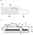
- Fig. 1 is a perspective view of a lighting device according to a first embodiment.
- Fig. 2 is a cross-sectional side view of the lighting device of Fig. 1 .
- Fig. 3 is an enlarged view of a part "A" shown in Fig. 2 .
- Fig. 1 is a perspective view showing the lighting device without a resin 160 shown in Fig. 2 .
- the lighting device may include a substrate 110, a first electrode layer 120, a second electrode layer 130, a light emitting device 140, a wavelength conversion layer 150 and the resin 160.
- the first electrode layer 120, the second electrode layer 130, the light emitting device 140, the wavelength conversion layer 150 and the resin 160 may be disposed on the substrate 110.
- the substrate 110 functions as a body.
- a printed circuit board (PCB), silicon wafer, resin, and sub-mount may be variously used as the substrate 110. Also, depending on the material of the substrate 110, the substrate 110 may be divided into a plastic package, a ceramic package, a metal package, etc.
- An insulation layer may be disposed on the substrate 110.
- the insulation layer functions to disconnect the electrical connections between other components.
- the insulation layer is not necessarily disposed.
- the first electrode layer 120 and the second electrode layer 130 are disposed on the top surface 111 of the substrate 110.
- the first electrode layer 120 and the second electrode layer 130 are disposed separately from each other on the top surface 111 of the substrate 110. Therefore, the first electrode layer 120 and the second electrode layer 130 are electrically isolated from each other.
- the first electrode layer 120 and the second electrode layer 130 are made of a conductive material and are electrically connected to the light emitting device 140.
- the light emitting device 140 is disposed on the first electrode layer 120.
- the first electrode layer 120 is electrically connected to any one of two electrodes of the light emitting device 140.
- the light emitting device 140 may be disposed on the substrate 110 and may be disposed on the top surface of the first electrode layer 120.
- the light emitting device 140 may include a light emitting structure including a first conductive semiconductor layer, an active layer, and a second conductive semiconductor layer.
- the light emitting structure may be provided to have a structure in which the active layer is disposed between the first conductive semiconductor layer and the second conductive semiconductor layer.
- the first conductive semiconductor layer may include an n-type semiconductor layer and may be made of a material selected from GaN, AlN, AlGaN, InGaN, InN, InAlGaN, AlInN, AlGaAs, GaP, GaAs, GaAsP, AlGaInP and the like.
- the first conductive semiconductor layer may be doped with n-type dopant like Si, Ge, Sn, Se, Te, etc.
- the active layer is a layer in which electrons (or electron holes) injected through the first conductive semiconductor layer encounter electron holes (or electrons) injected through the second conductive semiconductor layer.
- the active layer emits light due to the energy band gap difference according to the constituent material thereof.
- the active layer may be formed to have at least any one of a single well structure, a multiple well structure, a quantum dot structure, and a quantum wire structure. However, there is no limit to this.
- the second conductive semiconductor layer may be implemented by a p-type semiconductor layer and may be made of a material selected from GaN, AlN, AlGaN, InGaN, InN, InAlGaN, AlInN, AlGaAs, GaP, GaAs, GaAsP, AlGaInP and the like.
- the second conductive semiconductor layer may be doped with p-type dopant like Mg, Zn, Ca, Sr, Ba, etc.
- the first conductive semiconductor layer may include the p-type semiconductor layer
- the second conductive semiconductor layer may include the n-type semiconductor layer
- a semiconductor layer including the n-type or p-type semiconductor layer may be formed under the second conductive semiconductor layer.
- the light emitting structure may include at least one of an n-p junction structure, a p-n junction structure, an n-p-n junction structure, and a p-n-p junction structure.
- the light emitting device 140 may selectively emit light from a visible light range to an ultraviolet range or may emit light having a unique color of a semiconductor material.
- One or more light emitting devices 140 may be disposed on the top surface of the first electrode layer 120.
- the light emitting device 140 may be a light emitting diode chip which emits red, green, blue visible light, etc., or a light emitting diode chip which emits ultraviolet light.
- the light emitting device 140 may include a first electrode (not shown) and a second electrode 147.
- the first electrode (not shown) of the light emitting device 140 is formed on the bottom surface of the light emitting device 140 and is electrically connected directly to the first electrode layer 120.
- the second electrode 147 is electrically connected to the second electrode layer 130 through a wire "W".
- a plurality of second electrodes 147 of one light emitting device 140 may be provided.
- two second electrodes 147 may be provided.
- Each of the two second electrodes 147 may be connected to the second electrode layer 130 through the wire.
- a luminance distribution of the entire light emitting surface is more even than that of the light emitting surface of the lighting device using one wire, and color deviation is reduced. Accordingly, the reliability of the light emitting device is improved and stain caused by the light emitting can be reduced.
- the wavelength conversion layer 150 is disposed on the light emitting device 140.
- the light emitting device 140 may include a top surface 141 on which the wavelength conversion layer 150 is disposed.
- the top surface 141 of the light emitting device 140 may include a light emitting surface 145 from which the light is actually emitted and a portion where the second electrode 147 which is connected to the wire "W" is disposed.
- the area of the light emitting surface 145 is less than the area of the top surface 141.
- the portion where the second electrode 147 is disposed may be a corner of the top surface 141.
- the wavelength conversion layer 150 is disposed on the light emitting device 140.
- the wavelength conversion layer 150 may be disposed on the top surface 141 of the light emitting device 140.
- the area of a bottom surface 153 of the wavelength conversion layer 150 is less than the area of the top surface 141 of the light emitting device 140. This is because the second electrode 147 of the light emitting device 140 may be disposed on the top surface 141 of the light emitting device 140.
- the area of the bottom surface 153 of the wavelength conversion layer 150 may be greater that the area of the light emitting surface 145 of the light emitting device 140. This intends to cause all of the light which is emitted from the light emitting surface 145 to pass through the wavelength conversion layer 150.
- the wavelength conversion layer 150 converts a part of first light which is emitted from the light emitting device 140 into second light having a wavelength different from that of the first light, and emits the other part of the first light together with the converted second light. Accordingly, the wavelength conversion layer 150 emits light mixed with the first light and the second light.
- the wavelength conversion layer 150 may include a fluorescent material so as to convert the first light into the second light.
- the fluorescent material may be a phosphor.
- the phosphor may include at least one of a red phosphor, a green phosphor, and a yellow phosphor.
- the phosphor may include at least one of garnet based phosphor (YAG, TAG), a silicate based phosphor, a nitride based phosphor and an oxynitride based phosphor.
- the phosphor included in the wavelength conversion layer 150 is excited by the first light emitted from the light emitting device 140, and then emits the second light having a wavelength different from that of the first light. Therefore, both the first light emitted from the light emitting device 140 and the second light excited by the first light and emitted may be emitted from a top surface 151 of the wavelength conversion layer 150.
- the wavelength conversion layer 150 may include a fluorescent material and a light transmitting material.
- an addition ratio of the color of the phosphor may be formed such that the green phosphor is more used than the red phosphor, and the yellow phosphor is more used than the green phosphor.
- the garnet phosphor (YAG), the silicate phosphor and the oxynitride phosphor may be used as the yellow phosphor.
- the silicate phosphor and the oxynitride phosphor may be used as the green phosphor.
- the nitride phosphor may be used as the red phosphor.
- the light transmitting material may be mixed with various kinds of the phosphors or may be configured by a layer including the red phosphor, a layer including the green phosphor and a layer including the yellow phosphor, which are formed separately from each other.
- the light transmitting material may be any one of resin, glass and ceramic.
- the top surface 151 of the wavelength conversion layer 150 may include a fine uneven structure 151a.
- the fine uneven structure 151a improves the light extraction efficiency of the wavelength conversion layer 150, so that the light extraction efficiency of the lighting device according to the first embodiment can be enhanced.
- the top surface 151 of the wavelength conversion layer 150 having the fine uneven structure 151a may have a surface roughness (Ra) larger than 0.1um.
- the top surface 151 of the wavelength conversion layer 150 may not have the fine uneven structure 151a. That is, the top surface 151 of the wavelength conversion layer 150 may be flat without the fine uneven structure 151a or may have an upwardly or downwardly convex curved surface.
- the top surface 151 of the wavelength conversion layer 150 may function as a light emitting surface of the lighting device according to the first embodiment.
- the light emitting device 140 and the wavelength conversion layer 150 may be bonded to each other by means of an adhesive agent (not shown).
- the adhesive agent (not shown) is able to prevent the light from leaking through a gap between the wavelength conversion layer 150 and the light emitting device 140. Since the light emitting device 140 and the wavelength conversion layer 150 are bonded to each other, the wavelength conversion layer 150 is able to stably guide the light of the light emitting device 140.
- the adhesive agent (not shown) may be made of a material having thermal resistance and light resistance, for example, silicon, fluoric resin, inorganic paste (glass).
- thermal resistance and light resistance of the adhesive agent (not shown) are increased, the reliability of the lighting device is improved, so that it is possible to enhance lumen maintenance.
- the resin 160 is disposed on the substrate 110.
- the resin 160 may be disposed to cover or bury the light emitting device 140 and a portion of the wavelength conversion layer 150.
- the resin 160 may cover the wire "W", the first electrode layer 120 and the second electrode layer 130.
- the resin 160 may have a white color.
- the white resin 160 may reflect incident light. Accordingly, the light extraction efficiency of the lighting device according to the first embodiment can be enhanced.
- a top surface 161 of the resin 160 may be located lower than the top surface 151 of the wavelength conversion layer 150.
- the top surface 161 of the resin 160 is located lower than the top surface 151 of the wavelength conversion layer 150, it is possible to prevent the liquefied resin 160 at the time of forming the resin 160 from overflowing into or being introduced into the top surface 151 of the wavelength conversion layer 150, or to reduce the introduction amount of the liquefied resin 160.
- the contamination or stain which is caused by the resin 160, on the top surface 151 of the wavelength conversion layer 150, i.e., the light emitting surface 151.
- the top surface 151 of the wavelength conversion layer 150 may be disposed at the same or similar height as the top surface 161 of the resin 160.
- the wire “W” may be selected considering the reliability, productivity, cost, performance, etc., of the product.
- the wire “W” may be made of a metallic material like Au, Ag, Cu, A1 and the like.
- the top surface 161 of the resin 160 is located lower than the top surface 151 of the wavelength conversion layer 150 in order to overcome the problem that the liquefied resin 160 overflows into or is introduced into the top surface 151 of the wavelength conversion layer 150.
- the thicknesses of the wavelength conversion layer 150 and the resin 160 are actually very small. Therefore, it is difficult to control the thicknesses in the manufacture of the lighting device.
- the liquefied resin 160 when the liquefied resin 160 is formed around the wavelength conversion layer 150 in the manufacture of the resin 160, the liquefied resin 160 comes in contact with the edge of the top surface 151 of the wavelength conversion layer 150 by a surface tension.
- the liquefied resin 160 in contact with the edge of the top surface 151 of the wavelength conversion layer 150 may spread on the top surface 151 of the wavelength conversion layer 150 along the fine uneven structure 151a of the wavelength conversion layer 150 by a capillary phenomenon.
- a lighting device capable of solving such a problem will be described below.
- Fig. 4 is a cross-sectional side view of a lighting device according to a second embodiment which is an embodiment of the invention.
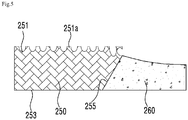
- Fig. 5 is an enlarged view of a part "B" shown in Fig. 4 .
- the lighting device according to the second embodiment may include the substrate 110, the first electrode layer 120, the second electrode layer 130, the light emitting device 140, a wavelength conversion layer 250, and a resin 260.
- the substrate 110, the first electrode layer 120, the second electrode layer 130, and the light emitting device 140 are the same as the substrate 110, the first electrode layer 120, the second electrode layer 130, and the light emitting device 140 shown in Figs. 1 to 3 , descriptions thereabout is replaced by the foregoing description.
- the wavelength conversion layer 250 and the resin 260 will be described in detail.
- the wavelength conversion layer 250 includes a top surface 251, a bottom surface 253, and a side surface 255.
- the side surface 255 is disposed between the top surface 251 and the bottom surface 253.
- a plurality of the side surfaces 255 is be provided according to the number of the sides of the top surface 251.
- the top surface 251 of the wavelength conversion layer 250 may include a fine uneven structure 251a.
- the fine uneven structure 251a is able to improve the light extraction efficiency of the wavelength conversion layer 250.
- the wavelength conversion layer 250 may be flat without the fine uneven structure 251a or may have an upwardly or downwardly convex portion thereof.
- the top surface 251 of the wavelength conversion layer 250 may be located higher than a top surface 261 of the resin 260.
- the top surface 251 of the wavelength conversion layer 250 is located higher than the top surface 261 of the resin 260, it is possible to prevent or reduce the possibility that the liquefied resin 260 at the time of forming the resin 160 overflows into or is introduced into the top surface 251 of the wavelength conversion layer 250.
- the top surface 251 of the wavelength conversion layer 250 may be disposed at the same or similar height as the top surface 261 of the resin 260.
- the side surface 255 includes a surface inclined at a predetermined angle with respect to the top surface 251 or the bottom surface 253.
- the side surface 255 may form a predetermined angle with the bottom surface 253.
- the side surface 255 will be described in detail with reference to Fig. 6 .
- Fig. 6 is a cross sectional view showing a light emitting device 140 and a wavelength conversion layer 250 shown in Fig. 4 .
- a first angle "a1" between the side surface 255 and the bottom surface 253 of the wavelength conversion layer 250 may be an obtuse angle
- a second angle “a2" between the side surface 255 and the top surface 251 may be an acute angle
- the first angle "a1” may be an angle between the side surface 255 and the light emitting surface 145 of the light emitting device 140.
- the first angle "a1” is an acute and the second angle “a2" is an obtuse angle as shown in (b) of Fig. 6
- the liquefied resin 260 shown in Fig. 4 is likely to spread on the top surface 251' along the side surface 255' of a wavelength conversion layer 250'. Therefore, it is preferable that the first angle "a1" is an obtuse and the second angle "a2" is an acute angle.
- the first angle “a1” may be from 95 degree (° ) to 115 degree (° ), and the second angle “a2" may be from 65 degree (° ) to 85 degree (° ).
- the liquefied resin 260 shown in Fig. 4 is likely to spread on the top surface 251 along the side surface 255 of the wavelength conversion layer 250 due to the surface tension by the liquefied resin 160 shown in Fig. 3 or due to the capillary phenomenon by the fine uneven structure 151a shown in Fig. 3 .
- the area of the top surface 251 is greater than the area of the bottom surface 253. At least one of the plurality of side surfaces 255 disposed between the top surface 251 and bottom surface 253 is a surface inclined toward the top surface 141 of the light emitting device 140 or the top surface of the substrate 110. As such, in the case where the area of the top surface 251 is greater than the area of the bottom surface 253 and at least one side surface 255 is a surface inclined toward the top surface 141 of the light emitting device 140 or the top surface of the substrate 110, when the resin 260 is formed, the liquefied resin 260 can be prevented from moving to the top surface 251 of the wavelength conversion layer 250. Accordingly, it is possible to prevent the contamination or stain, which is caused by the resin 260, on the top surface 251 of the wavelength conversion layer 250.
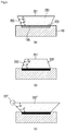
- Figs 7 to 8 are cross sectional views showing a modified example of the lighting device shown in Fig. 4 .
- the area of a top surface 351 and 451 of a wavelength conversion layer 350 and 450 is greater than the area of a bottom surface 353 and 453.
- a side surface 355 and 455 may be a curved surface.
- the side surface 355 shown in Fig. 7 may be concave toward the inside of the wavelength conversion layer 350.
- the side surface 455 shown in Fig. 8 may be convex toward the outside of the wavelength conversion layer 450.
- the area of the top surface 351 and 451 is greater than the area of the bottom surface 353 and 453 and the side surface 355 and 455 is a curved surface
- the liquefied resin 360 and 460 can be prevented from moving to the top surface 351 and 451 of the wavelength conversion layer 350 and 450. Accordingly, it is possible to prevent the contamination or stain, which is caused by the resin 360 and 460, on the top surface 351 and 451 of the wavelength conversion layer 350 and 450.
- the side surfaces 255, 355 and 455 of the wavelength conversion layer 250, 350 and 450 of the lighting devices according to the first and the second embodiments of the present invention may have recesses 255g, 355g and 455g.
- the resins 260, 360 and 460 may be disposed in the recesses 255g, 355g and 455g.
- the side surfaces 255, 355 and 455 of the wavelength conversion layer 250, 350 and 450 have the recesses 255g, 355g and 455g
- the liquefied resins 260, 360 and 460 when the resins 260, 360 and 460 are formed, the liquefied resins 260, 360 and 460 are formed, the liquefied resin 260, 360 and 460 can be prevented from moving to the top surface 251, 351 and 451 of the wavelength conversion layer 250, 350 and 450. Accordingly, it is possible to prevent the contamination or stain, which is caused by the resin 260, 360 and 460, on the top surface 251, 351 and 451 of the wavelength conversion layer 250, 350 and 450.
- the recesses 255g, 355g and 455g may be disposed in the lower portion of the side surfaces 255, 355 and 455 of the wavelength conversion layer 250, 350 and 450.
- the recesses 255g, 355g and 455g are disposed in the lower portion of the side surfaces 255, 355 and 455 of the wavelength conversion layer 250, 350 and 450, when the resin 260, 360 and 460 are formed, it is more difficult for the resin 260, 360 and 460 to move to the top surface 251, 351 and 451 of the wavelength conversion layer 250, 350 and 450.
- Fig. 9 is a view showing actual numerical values of the wavelength conversion layer 250 shown in Fig. 4 .
- the width of the top surface of the wavelength conversion layer 250 when the width of the top surface of the wavelength conversion layer 250 is set as 1, the width of the bottom surface 253 may be 0.98 and the horizon length and the vertical length of the bottom surface 253 may be the same as 0.98.
- the width of the bottom surface 253 of the wavelength conversion layer 250 may be less than 0.98.
- the width of the bottom surface 253 may be changed depending on the thickness of the wavelength conversion layer 250, that is, a distance between the top surface 251 and the bottom surface 253.
- the thickness of the wavelength conversion layer 250 may be changed depending on a color temperature which the lighting device targets.
Description
- Embodiments relate to a lighting device.
- A light emitting diode (LED) is an energy device for converting electric energy into light energy. Compared with an electric bulb, the LED has higher conversion efficiency, lower power consumption and a longer life span. As there advantages are widely known, more and more attentions are now paid to a lighting apparatus using the LED.
- The lighting apparatus using the LED are generally classified into a direct lighting apparatus and an indirect lighting apparatus. The direct lighting apparatus emits light emitted from the LED without changing the path of the light. The indirect lighting apparatus emits light emitted from the LED by changing the path of the light through reflecting means and so on. Compared with the direct lighting apparatus, the indirect lighting apparatus mitigates to some degree the intensified light emitted from the LED and protects the eyes of users.
- A conventional lighting device using the light emitting diode includes a lighting
device which uses a wavelength conversion layer on the light emitting surface of the light emitting diode. - The lighting device forms a white resin around the wavelength conversion layer. In this case, the white resin moves on the top surface of the wavelength conversion layer, so that the wavelength conversion layer is contaminated or stained by the white resin.
-
EP 2479812 A2 discloses a semiconductor light-emitting device including a wavelength converting layer in order to emit various colored lights including white light.US 2012140506 A1 ,EP 2555262 A2 ,EP 2511965 A2 ,JP 2010 219324 - One embodiment is a lighting device which includes: a substrate; a light emitting device disposed on the substrate; a wavelength conversion layer which is disposed on the light emitting device and converts a part of first light emitted from the light emitting device into second light having a wavelength different from that of the first light; and a resin which is disposed on the substrate and buries the light emitting device and at least a portion of the wavelength conversion layer. The wavelength conversion layer comprises a bottom surface on which the first light is incident, a top surface through which the second light is emitted and a side surface between the bottom surface and the top surface. An area of the top surface of the wavelength conversion layer is greater than that of the bottom surface of the wavelength conversion layer. The side surface of the wavelength conversion layer is inclined at a predetermined angle with respect to the top surface or the bottom surface. An area of the bottom surface of the wavelength conversion layer is less than an area of a top surface of the light emitting device. An area of the bottom surface of the wavelength conversion layer is less than an area of the top surface of the light emitting device. The angle between the side surface of the wavelength conversion layer and the bottom surface of the wavelength conversion layer may be an obtuse angle. The angle between the side surface of the wavelength conversion layer and the top surface of the wavelength conversion layer may be an acute angle.
- The angle between the side surface of the wavelength conversion layer and the bottom surface of the wavelength conversion layer may be 95 degree to 115 degree. The angle between the side surface of the wavelength conversion layer and the top surface of the wavelength conversion layer may be from 65 degree to 85 degree.
- The top surface of the wavelength conversion layer may include a fine uneven structure.
- The resin includes a top surface. The top surface of the resin may be located lower than the top surface of the wavelength conversion layer.
- The wavelength conversion layer may include a phosphor. The phosphor may include at least one of a red phosphor, a green phosphor, and a yellow phosphor.
- Another embodiment is a lighting device which includes: a substrate; a light emitting device disposed on the substrate; a wavelength conversion layer which is disposed on the light emitting device and converts a part of first light emitted from the light emitting device into second light having a wavelength different from that of the first light; and a resin which is disposed on the substrate and buries the light emitting device and at least a portion of the wavelength conversion layer. The wavelength conversion layer comprises a bottom surface on which the first light is incident, a top surface through which the second light is emitted and a side surface between the bottom surface and the top surface. An area of the top surface of the wavelength conversion layer is greater than that of the bottom surface of the wavelength conversion layer. The side surface of the wavelength conversion layer is a curved surface. An area of the bottom surface of the wavelength conversion layer is less than an area of a top surface of the light emitting device. The side surface may be concave toward the inside of the wavelength conversion layer.
- The side surface may be convex toward the outside of the wavelength conversion layer.
- The top surface of the wavelength conversion layer comprises a fine uneven structure.
- The resin includes a top surface. The top surface of the resin may be located lower than the top surface of the wavelength conversion layer.
- The wavelength conversion layer may include a phosphor. The phosphor may include at least one of a red phosphor, a green phosphor, and a yellow phosphor.
- The side surface of the wavelength conversion layer may comprise a recess in which the resin is disposed.
- The side surface of the wavelength conversion layer may include an upper portion and a lower portion. The recess may be formed in the lower portion.
- The top surface of the wavelength conversion layer may include a fine uneven structure.
- The resin includes a top surface. The top surface of the resin may be located lower than the top surface of the wavelength conversion layer.
- The wavelength conversion layer may include a phosphor. The phosphor may include at least one of a red phosphor, a green phosphor, and a yellow phosphor. This disclosure relates to embodiments from which some are embodiments of the invention.
- Arrangements and embodiments may be described in detail with reference to the following drawings in which like reference numerals refer to like elements and wherein:
-
Fig. 1 is a perspective view of a lighting device according to a first embodiment; -
Fig. 2 is a cross-sectional side view of the lighting device ofFig. 1 ; -
Fig. 3 is an enlarged view of a part "A" shown inFig. 2 ; -
Fig. 4 is a cross-sectional side view of a lighting device according to a second embodiment, which is an embodiment according to the invention. -
Fig. 5 is an enlarged view of a part "B" shown inFig. 4 ; -
Fig. 6 is a cross sectional view showing alight emitting device 140 and awavelength conversion layer 250 shown inFig. 4 ; -
Figs 7 to 8 are cross sectional views showing a modified example of the lighting device shown inFig. 4 ; and -
Fig. 9 is a view showing actual numerical values of thewavelength conversion layer 250 shown inFig. 4 . - A thickness or a size of each layer may be magnified, omitted or schematically shown for the purpose of convenience and clearness of description. The size of each component may not necessarily mean its actual size.
- It should be understood that when an element is referred to as being 'on' or "under" another element, it may be directly on/under the element, and/or one or more intervening elements may also be present. When an element is referred to as being 'on' or 'under', 'under the element' as well as 'on the element' may be included based on the element.
- An embodiment may be described in detail with reference to the accompanying drawings.
-
Fig. 1 is a perspective view of a lighting device according to a first embodiment.Fig. 2 is a cross-sectional side view of the lighting device ofFig. 1 .Fig. 3 is an enlarged view of a part "A" shown inFig. 2 . Here,Fig. 1 is a perspective view showing the lighting device without aresin 160 shown inFig. 2 . - Referring to
Figs. 1 to 3 , the lighting device according to the first embodiment may include asubstrate 110, afirst electrode layer 120, asecond electrode layer 130, alight emitting device 140, awavelength conversion layer 150 and theresin 160. - The
first electrode layer 120, thesecond electrode layer 130, thelight emitting device 140, thewavelength conversion layer 150 and theresin 160 may be disposed on thesubstrate 110. - The
substrate 110 functions as a body. A printed circuit board (PCB), silicon wafer, resin, and sub-mount may be variously used as thesubstrate 110. Also, depending on the material of thesubstrate 110, thesubstrate 110 may be divided into a plastic package, a ceramic package, a metal package, etc. - An insulation layer (not shown) may be disposed on the
substrate 110. The insulation layer (not shown) functions to disconnect the electrical connections between other components. However, when thesubstrate 110 is made of a nonconductive material, the insulation layer (not shown) is not necessarily disposed. - The
first electrode layer 120 and thesecond electrode layer 130 are disposed on thetop surface 111 of thesubstrate 110. Thefirst electrode layer 120 and thesecond electrode layer 130 are disposed separately from each other on thetop surface 111 of thesubstrate 110. Therefore, thefirst electrode layer 120 and thesecond electrode layer 130 are electrically isolated from each other. - The
first electrode layer 120 and thesecond electrode layer 130 are made of a conductive material and are electrically connected to thelight emitting device 140. - The
light emitting device 140 is disposed on thefirst electrode layer 120. Thefirst electrode layer 120 is electrically connected to any one of two electrodes of thelight emitting device 140. - The
light emitting device 140 may be disposed on thesubstrate 110 and may be disposed on the top surface of thefirst electrode layer 120. - The
light emitting device 140 may include a light emitting structure including a first conductive semiconductor layer, an active layer, and a second conductive semiconductor layer. For example, the light emitting structure may be provided to have a structure in which the active layer is disposed between the first conductive semiconductor layer and the second conductive semiconductor layer. - The first conductive semiconductor layer may include an n-type semiconductor layer and may be made of a material selected from GaN, AlN, AlGaN, InGaN, InN, InAlGaN, AlInN, AlGaAs, GaP, GaAs, GaAsP, AlGaInP and the like. The first conductive semiconductor layer may be doped with n-type dopant like Si, Ge, Sn, Se, Te, etc.
- The active layer is a layer in which electrons (or electron holes) injected through the first conductive semiconductor layer encounter electron holes (or electrons) injected through the second conductive semiconductor layer. The active layer emits light due to the energy band gap difference according to the constituent material thereof. The active layer may be formed to have at least any one of a single well structure, a multiple well structure, a quantum dot structure, and a quantum wire structure. However, there is no limit to this.
- The second conductive semiconductor layer may be implemented by a p-type semiconductor layer and may be made of a material selected from GaN, AlN, AlGaN, InGaN, InN, InAlGaN, AlInN, AlGaAs, GaP, GaAs, GaAsP, AlGaInP and the like. The second conductive semiconductor layer may be doped with p-type dopant like Mg, Zn, Ca, Sr, Ba, etc.
- Meanwhile, the first conductive semiconductor layer may include the p-type semiconductor layer, and the second conductive semiconductor layer may include the n-type semiconductor layer. Also, a semiconductor layer including the n-type or p-type semiconductor layer may be formed under the second conductive semiconductor layer. Accordingly, the light emitting structure may include at least one of an n-p junction structure, a p-n junction structure, an n-p-n junction structure, and a p-n-p junction structure.
- The
light emitting device 140 may selectively emit light from a visible light range to an ultraviolet range or may emit light having a unique color of a semiconductor material. - One or more light emitting
devices 140 may be disposed on the top surface of thefirst electrode layer 120. Thelight emitting device 140 may be a light emitting diode chip which emits red, green, blue visible light, etc., or a light emitting diode chip which emits ultraviolet light. - The
light emitting device 140 may include a first electrode (not shown) and asecond electrode 147. The first electrode (not shown) of thelight emitting device 140 is formed on the bottom surface of thelight emitting device 140 and is electrically connected directly to thefirst electrode layer 120. Thesecond electrode 147 is electrically connected to thesecond electrode layer 130 through a wire "W". - Here, as shown in
Fig. 1 , a plurality ofsecond electrodes 147 of onelight emitting device 140 may be provided. For example, twosecond electrodes 147 may be provided. Each of the twosecond electrodes 147 may be connected to thesecond electrode layer 130 through the wire. When thesecond electrode layer 130 is connected to thesecond electrode 147 of thelight emitting device 140 through the plurality of wires, a luminance distribution of the entire light emitting surface is more even than that of the light emitting surface of the lighting device using one wire, and color deviation is reduced. Accordingly, the reliability of the light emitting device is improved and stain caused by the light emitting can be reduced. - The
wavelength conversion layer 150 is disposed on thelight emitting device 140. Thelight emitting device 140 may include atop surface 141 on which thewavelength conversion layer 150 is disposed. - The
top surface 141 of thelight emitting device 140 may include alight emitting surface 145 from which the light is actually emitted and a portion where thesecond electrode 147 which is connected to the wire "W" is disposed. Here, the area of thelight emitting surface 145 is less than the area of thetop surface 141. The portion where thesecond electrode 147 is disposed may be a corner of thetop surface 141. - The
wavelength conversion layer 150 is disposed on thelight emitting device 140. Thewavelength conversion layer 150 may be disposed on thetop surface 141 of thelight emitting device 140. According to the invention, the area of abottom surface 153 of thewavelength conversion layer 150 is less than the area of thetop surface 141 of thelight emitting device 140. This is because thesecond electrode 147 of thelight emitting device 140 may be disposed on thetop surface 141 of thelight emitting device 140. - The area of the
bottom surface 153 of thewavelength conversion layer 150 may be greater that the area of thelight emitting surface 145 of thelight emitting device 140. This intends to cause all of the light which is emitted from thelight emitting surface 145 to pass through thewavelength conversion layer 150. - The
wavelength conversion layer 150 converts a part of first light which is emitted from thelight emitting device 140 into second light having a wavelength different from that of the first light, and emits the other part of the first light together with the converted second light. Accordingly, thewavelength conversion layer 150 emits light mixed with the first light and the second light. - The
wavelength conversion layer 150 may include a fluorescent material so as to convert the first light into the second light. Here, the fluorescent material may be a phosphor. The phosphor may include at least one of a red phosphor, a green phosphor, and a yellow phosphor. The phosphor may include at least one of garnet based phosphor (YAG, TAG), a silicate based phosphor, a nitride based phosphor and an oxynitride based phosphor. - The phosphor included in the
wavelength conversion layer 150 is excited by the first light emitted from thelight emitting device 140, and then emits the second light having a wavelength different from that of the first light. Therefore, both the first light emitted from thelight emitting device 140 and the second light excited by the first light and emitted may be emitted from atop surface 151 of thewavelength conversion layer 150. - The
wavelength conversion layer 150 may include a fluorescent material and a light transmitting material. - When the light transmitting material is mixed with many kinds of phosphors, an addition ratio of the color of the phosphor may be formed such that the green phosphor is more used than the red phosphor, and the yellow phosphor is more used than the green phosphor. The garnet phosphor (YAG), the silicate phosphor and the oxynitride phosphor may be used as the yellow phosphor. The silicate phosphor and the oxynitride phosphor may be used as the green phosphor. The nitride phosphor may be used as the red phosphor. The light transmitting material may be mixed with various kinds of the phosphors or may be configured by a layer including the red phosphor, a layer including the green phosphor and a layer including the yellow phosphor, which are formed separately from each other.
- The light transmitting material may be any one of resin, glass and ceramic.
- As shown in
Fig. 3 , thetop surface 151 of thewavelength conversion layer 150 may include a fineuneven structure 151a. The fineuneven structure 151a improves the light extraction efficiency of thewavelength conversion layer 150, so that the light extraction efficiency of the lighting device according to the first embodiment can be enhanced. Thetop surface 151 of thewavelength conversion layer 150 having the fineuneven structure 151a may have a surface roughness (Ra) larger than 0.1um. - Here, the
top surface 151 of thewavelength conversion layer 150 may not have the fineuneven structure 151a. That is, thetop surface 151 of thewavelength conversion layer 150 may be flat without the fineuneven structure 151a or may have an upwardly or downwardly convex curved surface. - The
top surface 151 of thewavelength conversion layer 150 may function as a light emitting surface of the lighting device according to the first embodiment. - The
light emitting device 140 and thewavelength conversion layer 150 may be bonded to each other by means of an adhesive agent (not shown). The adhesive agent (not shown) is able to prevent the light from leaking through a gap between thewavelength conversion layer 150 and thelight emitting device 140. Since thelight emitting device 140 and thewavelength conversion layer 150 are bonded to each other, thewavelength conversion layer 150 is able to stably guide the light of thelight emitting device 140. - The adhesive agent (not shown) may be made of a material having thermal resistance and light resistance, for example, silicon, fluoric resin, inorganic paste (glass). When the thermal resistance and light resistance of the adhesive agent (not shown) are increased, the reliability of the lighting device is improved, so that it is possible to enhance lumen maintenance.
- The
resin 160 is disposed on thesubstrate 110. Theresin 160 may be disposed to cover or bury thelight emitting device 140 and a portion of thewavelength conversion layer 150. Theresin 160 may cover the wire "W", thefirst electrode layer 120 and thesecond electrode layer 130. - The
resin 160 may have a white color. Thewhite resin 160 may reflect incident light. Accordingly, the light extraction efficiency of the lighting device according to the first embodiment can be enhanced. - A
top surface 161 of theresin 160 may be located lower than thetop surface 151 of thewavelength conversion layer 150. When thetop surface 161 of theresin 160 is located lower than thetop surface 151 of thewavelength conversion layer 150, it is possible to prevent the liquefiedresin 160 at the time of forming theresin 160 from overflowing into or being introduced into thetop surface 151 of thewavelength conversion layer 150, or to reduce the introduction amount of the liquefiedresin 160. As a result, it is possible to reduce the contamination or stain, which is caused by theresin 160, on thetop surface 151 of thewavelength conversion layer 150, i.e., thelight emitting surface 151. - Here, the
top surface 151 of thewavelength conversion layer 150 may be disposed at the same or similar height as thetop surface 161 of theresin 160. - The wire "W" may be selected considering the reliability, productivity, cost, performance, etc., of the product. The wire "W" may be made of a metallic material like Au, Ag, Cu, A1 and the like.
- In the lighting device according to the first embodiment, when the
resin 160 is formed, thetop surface 161 of theresin 160 is located lower than thetop surface 151 of thewavelength conversion layer 150 in order to overcome the problem that the liquefiedresin 160 overflows into or is introduced into thetop surface 151 of thewavelength conversion layer 150. However, the thicknesses of thewavelength conversion layer 150 and theresin 160 are actually very small. Therefore, it is difficult to control the thicknesses in the manufacture of the lighting device. - As shown in
Fig. 3 , when the liquefiedresin 160 is formed around thewavelength conversion layer 150 in the manufacture of theresin 160, the liquefiedresin 160 comes in contact with the edge of thetop surface 151 of thewavelength conversion layer 150 by a surface tension. Here, in a case where thetop surface 151 of thewavelength conversion layer 150 has the fineuneven structure 151a, the liquefiedresin 160 in contact with the edge of thetop surface 151 of thewavelength conversion layer 150 may spread on thetop surface 151 of thewavelength conversion layer 150 along the fineuneven structure 151a of thewavelength conversion layer 150 by a capillary phenomenon. - A lighting device capable of solving such a problem will be described below.
-
Fig. 4 is a cross-sectional side view of a lighting device according to a second embodiment which is an embodiment of the invention.Fig. 5 is an enlarged view of a part "B" shown inFig. 4 . - Referring to
Figs. 4 to 5 , the lighting device according to the second embodiment may include thesubstrate 110, thefirst electrode layer 120, thesecond electrode layer 130, thelight emitting device 140, awavelength conversion layer 250, and aresin 260. - Here, since the
substrate 110, thefirst electrode layer 120, thesecond electrode layer 130, and thelight emitting device 140 are the same as thesubstrate 110, thefirst electrode layer 120, thesecond electrode layer 130, and thelight emitting device 140 shown inFigs. 1 to 3 , descriptions thereabout is replaced by the foregoing description. Hereafter, thewavelength conversion layer 250 and theresin 260 will be described in detail. - The
wavelength conversion layer 250 includes atop surface 251, abottom surface 253, and aside surface 255. Theside surface 255 is disposed between thetop surface 251 and thebottom surface 253. A plurality of the side surfaces 255 is be provided according to the number of the sides of thetop surface 251. - As shown in
Fig. 5 , thetop surface 251 of thewavelength conversion layer 250 may include a fineuneven structure 251a. The fineuneven structure 251a is able to improve the light extraction efficiency of thewavelength conversion layer 250. Here, thewavelength conversion layer 250 may be flat without the fineuneven structure 251a or may have an upwardly or downwardly convex portion thereof. - The
top surface 251 of thewavelength conversion layer 250 may be located higher than atop surface 261 of theresin 260. When thetop surface 251 of thewavelength conversion layer 250 is located higher than thetop surface 261 of theresin 260, it is possible to prevent or reduce the possibility that the liquefiedresin 260 at the time of forming theresin 160 overflows into or is introduced into thetop surface 251 of thewavelength conversion layer 250. Here, thetop surface 251 of thewavelength conversion layer 250 may be disposed at the same or similar height as thetop surface 261 of theresin 260. - The
side surface 255 includes a surface inclined at a predetermined angle with respect to thetop surface 251 or thebottom surface 253. For example, theside surface 255 may form a predetermined angle with thebottom surface 253. Theside surface 255 will be described in detail with reference toFig. 6 . -
Fig. 6 is a cross sectional view showing alight emitting device 140 and awavelength conversion layer 250 shown inFig. 4 . - Referring to (a) of
Fig. 6 , a first angle "a1" between theside surface 255 and thebottom surface 253 of thewavelength conversion layer 250 may be an obtuse angle, and a second angle "a2" between theside surface 255 and thetop surface 251 may be an acute angle. Here, the first angle "a1" may be an angle between theside surface 255 and thelight emitting surface 145 of thelight emitting device 140. - Here, when the first angle "a1" is an acute and the second angle "a2" is an obtuse angle as shown in (b) of
Fig. 6 , the liquefiedresin 260 shown inFig. 4 is likely to spread on the top surface 251' along the side surface 255' of a wavelength conversion layer 250'. Therefore, it is preferable that the first angle "a1" is an obtuse and the second angle "a2" is an acute angle. - Referring back to (a) of
Fig. 6 , more specifically, the first angle "a1" may be from 95 degree (° ) to 115 degree (° ), and the second angle "a2" may be from 65 degree (° ) to 85 degree (° ). - Here, when the first angle "a1" is less than 95 degree (° ) and the second angle "a2" is greater than 85 degree (° ), the liquefied
resin 260 shown inFig. 4 is likely to spread on thetop surface 251 along theside surface 255 of thewavelength conversion layer 250 due to the surface tension by the liquefiedresin 160 shown inFig. 3 or due to the capillary phenomenon by the fineuneven structure 151a shown inFig. 3 . - Meanwhile, when the first angle "a1" is greater than 115 degree (° ) and the second angle "a2" is less than 65 degree (° ), an
edge 257 of the upper portion of awavelength conversion layer 250" becomes thinner and sharper as shown in (c) ofFig. 6 , and thus, is fragile by an external impact. - The area of the
top surface 251 is greater than the area of thebottom surface 253. At least one of the plurality of side surfaces 255 disposed between thetop surface 251 andbottom surface 253 is a surface inclined toward thetop surface 141 of thelight emitting device 140 or the top surface of thesubstrate 110. As such, in the case where the area of thetop surface 251 is greater than the area of thebottom surface 253 and at least oneside surface 255 is a surface inclined toward thetop surface 141 of thelight emitting device 140 or the top surface of thesubstrate 110, when theresin 260 is formed, the liquefiedresin 260 can be prevented from moving to thetop surface 251 of thewavelength conversion layer 250. Accordingly, it is possible to prevent the contamination or stain, which is caused by theresin 260, on thetop surface 251 of thewavelength conversion layer 250. -
Figs 7 to 8 are cross sectional views showing a modified example of the lighting device shown inFig. 4 . - Referring to
Figs. 7 to 8 , the area of atop surface wavelength conversion layer side surface - The
side surface 355 shown inFig. 7 may be concave toward the inside of thewavelength conversion layer 350. Theside surface 455 shown inFig. 8 may be convex toward the outside of thewavelength conversion layer 450. - As such, in the case where the area of the
top surface side surface resin resin top surface wavelength conversion layer resin top surface wavelength conversion layer - As shown in
Figs. 4 and7 to 8 , the side surfaces 255, 355 and 455 of thewavelength conversion layer recesses resins recesses wavelength conversion layer recesses resins resins resin top surface wavelength conversion layer resin top surface wavelength conversion layer - Here, the
recesses wavelength conversion layer recesses wavelength conversion layer resin resin top surface wavelength conversion layer -
Fig. 9 is a view showing actual numerical values of thewavelength conversion layer 250 shown inFig. 4 . - Referring to
Fig. 9 , when the width of the top surface of thewavelength conversion layer 250 is set as 1, the width of thebottom surface 253 may be 0.98 and the horizon length and the vertical length of thebottom surface 253 may be the same as 0.98. - Here, the width of the
bottom surface 253 of thewavelength conversion layer 250 may be less than 0.98. The width of thebottom surface 253 may be changed depending on the thickness of thewavelength conversion layer 250, that is, a distance between thetop surface 251 and thebottom surface 253. The thickness of thewavelength conversion layer 250 may be changed depending on a color temperature which the lighting device targets. - The appearances of such phrases in various places in the specification are not necessarily all referring to the same embodiment. Further, when a particular feature, structure, or characteristic is described in connection with any embodiment, it is submitted that it is within the purview of one skilled in the art to affect such feature, structure, or characteristic in connection with other ones of the embodiments.
- Although embodiments have been described with reference to a number of illustrative embodiments thereof, it should be understood that numerous other modifications and embodiments can be devised by those skilled in the art that will fall within the scope of the invention defined by the appended claims.
Claims (12)
- A lighting device comprising:a substrate (110);a light emitting device (140) disposed on the substrate (110);a wavelength conversion layer (250) which is disposed on the light emitting device (140) and converts a part of first light emitted from the light emitting device (140) into second light having a wavelength different from that of the first light; anda resin (260) which is disposed on the substrate (110) and buries the light emitting device (140) and at least a portion of the wavelength conversion layer (250),wherein the wavelength conversion layer (250) comprises a bottom surface (253) on which the first light is incident, a top surface (251) through which the second light is emitted and a side surface between the bottom surface (253) and the top surface (251),wherein an area of the top surface (251) of the wavelength conversion layer (250) is greater than that of the bottom surface (253) of the wavelength conversion layer (250),wherein the side surface (255) of the wavelength conversion layer (250) is inclined at a predetermined angle with respect to the top surface (251) or the bottom surface (253),characterized in that an area of the bottom surface (253) of the wavelength conversion layer (250) is less than an area of a top surface (141) of the light emitting device (140).
- The lighting device of claim 1,wherein the angle between the side surface of the wavelength conversion layer (250) and the bottom surface (253) of the wavelength conversion layer (250) is an obtuse angle,and wherein the angle between the side surface of the wavelength conversion layer (250) and the top surface (251) of the wavelength conversion layer (250) is an acute angle.
- The lighting device of claim 1,wherein the angle between the side surface of the wavelength conversion layer (250) and the bottom surface (253) of the wavelength conversion layer (250) is 95 degree to 115 degree,and wherein the angle between the side surface of the wavelength conversion layer (250) and the top surface (251) of the wavelength conversion layer (250) is from 65 degree to 85 degree.
- A lighting device comprising:a substrate (110);a light emitting device (140) disposed on the substrate (110);a wavelength conversion layer (250) which is disposed on the light emitting device (140) and converts a part of first light emitted from the light emitting device (140) into second light having a wavelength different from that of the first light; anda resin (260) which is disposed on the substrate (110) and buries the light emitting device (140) and at least a portion of the wavelength conversion layer (250),wherein the wavelength conversion layer (250) comprises a bottom surface (253) on which the first light is incident, a top surface (251) through which the second light is emitted and a side surface between the bottom surface (253) and the top surface (251),wherein an area of the top surface (251) of the wavelength conversion layer (250) is greater than that of the bottom surface (253) of the wavelength conversion layer (250),wherein the side surface of the wavelength conversion layer (250) is a curved surface,characterized in that an area of the bottom surface (253) of the wavelength conversion layer (250) is less than an area of a top surface (141) of the light emitting device (140).
- The lighting device of claim 4, wherein the side surface is concave toward the inside of the wavelength conversion layer (250).
- The lighting device of claim 4, wherein the side surface is convex toward the outside of the wavelength conversion layer (250).
- The lighting device of any one of claims 1 to 6,wherein the side surface of the wavelength conversion layer (250) comprises a recess in which the resin (260) is disposed.
- The lighting device of claim 7,wherein the side surface of the wavelength conversion layer (250) comprises an upper portion and a lower portion,and wherein the recess is formed in the lower portion.
- The lighting device of any one of claims 1 to 8, wherein the top surface (251) of the wavelength conversion layer (250) comprises a fine uneven structure.
- The lighting device of any one of claims 1 to 9,wherein the resin (260) comprises a top surface (261),and wherein the top surface (261) of the resin (260) is located lower than the top surface (251) of the wavelength conversion layer (250).
- The lighting device of any one of claims 1 to 10,wherein the wavelength conversion layer (250) comprises a phosphor,and wherein the phosphor comprises at least one of a red phosphor, a green phosphor, and a yellow phosphor.
- The lighting device of any one of claims 1 to 11,wherein the light emitting device (140) comprises a light emitting surface which emits the first light,and wherein an area of the bottom surface (253) of the wavelength conversion layer (250) is greater than that of the light emitting surface of the light emitting device (140).
Applications Claiming Priority (1)
| Application Number | Priority Date | Filing Date | Title |
|---|---|---|---|
| KR1020140056207A KR20150129356A (en) | 2014-05-12 | 2014-05-12 | Lighting device |
Publications (2)
| Publication Number | Publication Date |
|---|---|
| EP2945196A1 EP2945196A1 (en) | 2015-11-18 |
| EP2945196B1 true EP2945196B1 (en) | 2018-03-28 |
Family
ID=53051756
Family Applications (1)
| Application Number | Title | Priority Date | Filing Date |
|---|---|---|---|
| EP15166955.3A Active EP2945196B1 (en) | 2014-05-12 | 2015-05-08 | Light emitting diode having wavelength conversion layer |
Country Status (4)
| Country | Link |
|---|---|
| US (1) | US9893246B2 (en) |
| EP (1) | EP2945196B1 (en) |
| KR (1) | KR20150129356A (en) |
| CN (1) | CN105098035A (en) |
Families Citing this family (10)
| Publication number | Priority date | Publication date | Assignee | Title |
|---|---|---|---|---|
| WO2016094422A1 (en) * | 2014-12-08 | 2016-06-16 | Koninklijke Philips N.V. | Wavelength converted semiconductor light emitting device |
| JP6217705B2 (en) * | 2015-07-28 | 2017-10-25 | 日亜化学工業株式会社 | Light emitting device and manufacturing method thereof |
| JP6399017B2 (en) * | 2016-02-29 | 2018-10-03 | 日亜化学工業株式会社 | Light emitting device |
| CN107946441A (en) * | 2016-10-12 | 2018-04-20 | 亿光电子工业股份有限公司 | Light-emitting device and light-emitting diode encapsulation structure |
| JP7269792B2 (en) * | 2019-05-16 | 2023-05-09 | スタンレー電気株式会社 | light emitting device |
| JP7271302B2 (en) * | 2019-05-16 | 2023-05-11 | スタンレー電気株式会社 | semiconductor light emitting device |
| JP7233301B2 (en) * | 2019-05-29 | 2023-03-06 | スタンレー電気株式会社 | semiconductor light emitting device |
| CN112054110A (en) * | 2019-06-05 | 2020-12-08 | 比亚迪股份有限公司 | LED packaging structure and car lamp thereof |
| JP2021136377A (en) * | 2020-02-28 | 2021-09-13 | 日亜化学工業株式会社 | Wavelength conversion member and light-emitting device |
| JP2023140834A (en) * | 2022-03-23 | 2023-10-05 | スタンレー電気株式会社 | Light-emitting device and method for manufacturing light-emitting device |
Family Cites Families (12)
| Publication number | Priority date | Publication date | Assignee | Title |
|---|---|---|---|---|
| JP5255421B2 (en) * | 2008-12-15 | 2013-08-07 | 株式会社小糸製作所 | Light emitting module, method for manufacturing light emitting module, and lamp unit |
| JP5326705B2 (en) * | 2009-03-17 | 2013-10-30 | 日亜化学工業株式会社 | Light emitting device |
| DE102010028407B4 (en) * | 2010-04-30 | 2021-01-14 | OSRAM Opto Semiconductors Gesellschaft mit beschränkter Haftung | Optoelectronic component and method for producing an optoelectronic component |
| US8455907B2 (en) * | 2010-06-16 | 2013-06-04 | Stanley Electric Co., Ltd. | Semiconductor light emitting device having an optical plate including a meniscus control structure and method of manufacturing |
| JP5539849B2 (en) * | 2010-12-13 | 2014-07-02 | スタンレー電気株式会社 | Light emitting device and manufacturing method thereof |
| JP5588368B2 (en) * | 2011-01-24 | 2014-09-10 | スタンレー電気株式会社 | Light emitting device and manufacturing method thereof |
| JP5840377B2 (en) * | 2011-04-14 | 2016-01-06 | 日東電工株式会社 | Reflective resin sheet and method for manufacturing light-emitting diode device |
| JP2013038187A (en) * | 2011-08-05 | 2013-02-21 | Stanley Electric Co Ltd | Light-emitting device and method of manufacturing the same |
| TW201327926A (en) * | 2011-12-30 | 2013-07-01 | Ind Tech Res Inst | Light conversion structure and the light emitting device packaging structure using the same |
| WO2014024372A1 (en) * | 2012-08-10 | 2014-02-13 | パナソニック株式会社 | Semiconductor light-emitting device |
| KR20140032691A (en) * | 2012-09-07 | 2014-03-17 | 일진엘이디(주) | Light emitting device and method of manufacturing the same |
| JP6215525B2 (en) * | 2012-10-23 | 2017-10-18 | スタンレー電気株式会社 | Semiconductor light emitting device |
-
2014
- 2014-05-12 KR KR1020140056207A patent/KR20150129356A/en not_active Application Discontinuation
-
2015
- 2015-02-11 CN CN201510072413.5A patent/CN105098035A/en active Pending
- 2015-05-08 EP EP15166955.3A patent/EP2945196B1/en active Active
- 2015-05-11 US US14/708,397 patent/US9893246B2/en active Active
Non-Patent Citations (1)
| Title |
|---|
| None * |
Also Published As
| Publication number | Publication date |
|---|---|
| CN105098035A (en) | 2015-11-25 |
| KR20150129356A (en) | 2015-11-20 |
| US20150325757A1 (en) | 2015-11-12 |
| US9893246B2 (en) | 2018-02-13 |
| EP2945196A1 (en) | 2015-11-18 |
Similar Documents
| Publication | Publication Date | Title |
|---|---|---|
| EP2945196B1 (en) | Light emitting diode having wavelength conversion layer | |
| US9472742B2 (en) | Light emitting device and light unit having the same | |
| US9117986B2 (en) | Light emitting device | |
| EP3067927B1 (en) | Light emitting device based on light emitting diodes | |
| US10340433B2 (en) | Light emitting device | |
| US20190288168A1 (en) | Semiconductor device package | |
| US9312433B2 (en) | Light emitting element | |
| US8791495B2 (en) | Light emitting device package and lighting system | |
| US10256370B2 (en) | Light emitting device | |
| US10199540B2 (en) | Light emitting diode, light emitting diode package including same, and lighting system including same | |
| EP2315280B1 (en) | Light emitting diode package | |
| US20150053993A1 (en) | Semiconductor light emitting device | |
| US10541351B2 (en) | Light emitting diode having a current blocking layer | |
| US9660145B2 (en) | Light emitting device, light emitting device package having the same and light system having the same | |
| KR102195756B1 (en) | Lighting device packge | |
| KR102451107B1 (en) | Light emitting device and light emitting device package having thereof | |
| KR102282944B1 (en) | Lighting device | |
| KR102127440B1 (en) | Light Emitting Device Package | |
| KR102201186B1 (en) | Lighting device | |
| KR20120047184A (en) | Light emitting device and method for manufacuring the same | |
| KR20160002021A (en) | Lighting device | |
| KR20150138609A (en) | Light emitting device, method for fabricating the same, and light emitting device package | |
| KR20110055952A (en) | Light emitting diode package |
Legal Events
| Date | Code | Title | Description |
|---|---|---|---|
| PUAI | Public reference made under article 153(3) epc to a published international application that has entered the european phase |
Free format text: ORIGINAL CODE: 0009012 |
|
| AK | Designated contracting states |
Kind code of ref document: A1 Designated state(s): AL AT BE BG CH CY CZ DE DK EE ES FI FR GB GR HR HU IE IS IT LI LT LU LV MC MK MT NL NO PL PT RO RS SE SI SK SM TR |
|
| AX | Request for extension of the european patent |
Extension state: BA ME |
|
| 17P | Request for examination filed |
Effective date: 20160518 |
|
| RBV | Designated contracting states (corrected) |
Designated state(s): AL AT BE BG CH CY CZ DE DK EE ES FI FR GB GR HR HU IE IS IT LI LT LU LV MC MK MT NL NO PL PT RO RS SE SI SK SM TR |
|
| RAP1 | Party data changed (applicant data changed or rights of an application transferred) |
Owner name: LG INNOTEK CO., LTD. |
|
| GRAP | Despatch of communication of intention to grant a patent |
Free format text: ORIGINAL CODE: EPIDOSNIGR1 |
|
| RIC1 | Information provided on ipc code assigned before grant |
Ipc: H01L 33/56 20100101ALN20170925BHEP Ipc: H01L 33/50 20100101AFI20170925BHEP |
|
| INTG | Intention to grant announced |
Effective date: 20171025 |
|
| GRAS | Grant fee paid |
Free format text: ORIGINAL CODE: EPIDOSNIGR3 |
|
| GRAA | (expected) grant |
Free format text: ORIGINAL CODE: 0009210 |
|
| AK | Designated contracting states |
Kind code of ref document: B1 Designated state(s): AL AT BE BG CH CY CZ DE DK EE ES FI FR GB GR HR HU IE IS IT LI LT LU LV MC MK MT NL NO PL PT RO RS SE SI SK SM TR |
|
| REG | Reference to a national code |
Ref country code: GB Ref legal event code: FG4D |
|
| REG | Reference to a national code |
Ref country code: CH Ref legal event code: EP |
|
| REG | Reference to a national code |
Ref country code: AT Ref legal event code: REF Ref document number: 984143 Country of ref document: AT Kind code of ref document: T Effective date: 20180415 |
|
| REG | Reference to a national code |
Ref country code: IE Ref legal event code: FG4D |
|
| REG | Reference to a national code |
Ref country code: DE Ref legal event code: R096 Ref document number: 602015009232 Country of ref document: DE |
|
| REG | Reference to a national code |
Ref country code: FR Ref legal event code: PLFP Year of fee payment: 4 |
|
| PG25 | Lapsed in a contracting state [announced via postgrant information from national office to epo] |
Ref country code: LT Free format text: LAPSE BECAUSE OF FAILURE TO SUBMIT A TRANSLATION OF THE DESCRIPTION OR TO PAY THE FEE WITHIN THE PRESCRIBED TIME-LIMIT Effective date: 20180328 Ref country code: FI Free format text: LAPSE BECAUSE OF FAILURE TO SUBMIT A TRANSLATION OF THE DESCRIPTION OR TO PAY THE FEE WITHIN THE PRESCRIBED TIME-LIMIT Effective date: 20180328 Ref country code: NO Free format text: LAPSE BECAUSE OF FAILURE TO SUBMIT A TRANSLATION OF THE DESCRIPTION OR TO PAY THE FEE WITHIN THE PRESCRIBED TIME-LIMIT Effective date: 20180628 Ref country code: HR Free format text: LAPSE BECAUSE OF FAILURE TO SUBMIT A TRANSLATION OF THE DESCRIPTION OR TO PAY THE FEE WITHIN THE PRESCRIBED TIME-LIMIT Effective date: 20180328 |
|
| REG | Reference to a national code |
Ref country code: NL Ref legal event code: MP Effective date: 20180328 |
|
| REG | Reference to a national code |
Ref country code: LT Ref legal event code: MG4D |
|
| PG25 | Lapsed in a contracting state [announced via postgrant information from national office to epo] |
Ref country code: RS Free format text: LAPSE BECAUSE OF FAILURE TO SUBMIT A TRANSLATION OF THE DESCRIPTION OR TO PAY THE FEE WITHIN THE PRESCRIBED TIME-LIMIT Effective date: 20180328 Ref country code: GR Free format text: LAPSE BECAUSE OF FAILURE TO SUBMIT A TRANSLATION OF THE DESCRIPTION OR TO PAY THE FEE WITHIN THE PRESCRIBED TIME-LIMIT Effective date: 20180629 Ref country code: BG Free format text: LAPSE BECAUSE OF FAILURE TO SUBMIT A TRANSLATION OF THE DESCRIPTION OR TO PAY THE FEE WITHIN THE PRESCRIBED TIME-LIMIT Effective date: 20180628 Ref country code: LV Free format text: LAPSE BECAUSE OF FAILURE TO SUBMIT A TRANSLATION OF THE DESCRIPTION OR TO PAY THE FEE WITHIN THE PRESCRIBED TIME-LIMIT Effective date: 20180328 Ref country code: SE Free format text: LAPSE BECAUSE OF FAILURE TO SUBMIT A TRANSLATION OF THE DESCRIPTION OR TO PAY THE FEE WITHIN THE PRESCRIBED TIME-LIMIT Effective date: 20180328 |
|
| PG25 | Lapsed in a contracting state [announced via postgrant information from national office to epo] |
Ref country code: RO Free format text: LAPSE BECAUSE OF FAILURE TO SUBMIT A TRANSLATION OF THE DESCRIPTION OR TO PAY THE FEE WITHIN THE PRESCRIBED TIME-LIMIT Effective date: 20180328 Ref country code: ES Free format text: LAPSE BECAUSE OF FAILURE TO SUBMIT A TRANSLATION OF THE DESCRIPTION OR TO PAY THE FEE WITHIN THE PRESCRIBED TIME-LIMIT Effective date: 20180328 Ref country code: EE Free format text: LAPSE BECAUSE OF FAILURE TO SUBMIT A TRANSLATION OF THE DESCRIPTION OR TO PAY THE FEE WITHIN THE PRESCRIBED TIME-LIMIT Effective date: 20180328 Ref country code: PL Free format text: LAPSE BECAUSE OF FAILURE TO SUBMIT A TRANSLATION OF THE DESCRIPTION OR TO PAY THE FEE WITHIN THE PRESCRIBED TIME-LIMIT Effective date: 20180328 Ref country code: NL Free format text: LAPSE BECAUSE OF FAILURE TO SUBMIT A TRANSLATION OF THE DESCRIPTION OR TO PAY THE FEE WITHIN THE PRESCRIBED TIME-LIMIT Effective date: 20180328 Ref country code: AL Free format text: LAPSE BECAUSE OF FAILURE TO SUBMIT A TRANSLATION OF THE DESCRIPTION OR TO PAY THE FEE WITHIN THE PRESCRIBED TIME-LIMIT Effective date: 20180328 Ref country code: IT Free format text: LAPSE BECAUSE OF FAILURE TO SUBMIT A TRANSLATION OF THE DESCRIPTION OR TO PAY THE FEE WITHIN THE PRESCRIBED TIME-LIMIT Effective date: 20180328 |
|
| PG25 | Lapsed in a contracting state [announced via postgrant information from national office to epo] |
Ref country code: SM Free format text: LAPSE BECAUSE OF FAILURE TO SUBMIT A TRANSLATION OF THE DESCRIPTION OR TO PAY THE FEE WITHIN THE PRESCRIBED TIME-LIMIT Effective date: 20180328 Ref country code: SK Free format text: LAPSE BECAUSE OF FAILURE TO SUBMIT A TRANSLATION OF THE DESCRIPTION OR TO PAY THE FEE WITHIN THE PRESCRIBED TIME-LIMIT Effective date: 20180328 Ref country code: CZ Free format text: LAPSE BECAUSE OF FAILURE TO SUBMIT A TRANSLATION OF THE DESCRIPTION OR TO PAY THE FEE WITHIN THE PRESCRIBED TIME-LIMIT Effective date: 20180328 |
|
| REG | Reference to a national code |
Ref country code: CH Ref legal event code: PL |
|
| REG | Reference to a national code |
Ref country code: AT Ref legal event code: MK05 Ref document number: 984143 Country of ref document: AT Kind code of ref document: T Effective date: 20180328 |
|
| PG25 | Lapsed in a contracting state [announced via postgrant information from national office to epo] |
Ref country code: PT Free format text: LAPSE BECAUSE OF FAILURE TO SUBMIT A TRANSLATION OF THE DESCRIPTION OR TO PAY THE FEE WITHIN THE PRESCRIBED TIME-LIMIT Effective date: 20180730 |
|
| REG | Reference to a national code |
Ref country code: DE Ref legal event code: R097 Ref document number: 602015009232 Country of ref document: DE |
|
| REG | Reference to a national code |
Ref country code: BE Ref legal event code: MM Effective date: 20180531 |
|
| PG25 | Lapsed in a contracting state [announced via postgrant information from national office to epo] |
Ref country code: MC Free format text: LAPSE BECAUSE OF FAILURE TO SUBMIT A TRANSLATION OF THE DESCRIPTION OR TO PAY THE FEE WITHIN THE PRESCRIBED TIME-LIMIT Effective date: 20180328 Ref country code: AT Free format text: LAPSE BECAUSE OF FAILURE TO SUBMIT A TRANSLATION OF THE DESCRIPTION OR TO PAY THE FEE WITHIN THE PRESCRIBED TIME-LIMIT Effective date: 20180328 Ref country code: DK Free format text: LAPSE BECAUSE OF FAILURE TO SUBMIT A TRANSLATION OF THE DESCRIPTION OR TO PAY THE FEE WITHIN THE PRESCRIBED TIME-LIMIT Effective date: 20180328 |
|
| PLBE | No opposition filed within time limit |
Free format text: ORIGINAL CODE: 0009261 |
|
| STAA | Information on the status of an ep patent application or granted ep patent |
Free format text: STATUS: NO OPPOSITION FILED WITHIN TIME LIMIT |
|
| REG | Reference to a national code |
Ref country code: IE Ref legal event code: MM4A |
|
| PG25 | Lapsed in a contracting state [announced via postgrant information from national office to epo] |
Ref country code: LI Free format text: LAPSE BECAUSE OF NON-PAYMENT OF DUE FEES Effective date: 20180531 Ref country code: CH Free format text: LAPSE BECAUSE OF NON-PAYMENT OF DUE FEES Effective date: 20180531 |
|
| 26N | No opposition filed |
Effective date: 20190103 |
|
| PG25 | Lapsed in a contracting state [announced via postgrant information from national office to epo] |
Ref country code: LU Free format text: LAPSE BECAUSE OF NON-PAYMENT OF DUE FEES Effective date: 20180508 |
|
| PG25 | Lapsed in a contracting state [announced via postgrant information from national office to epo] |
Ref country code: IE Free format text: LAPSE BECAUSE OF NON-PAYMENT OF DUE FEES Effective date: 20180508 |
|
| PG25 | Lapsed in a contracting state [announced via postgrant information from national office to epo] |
Ref country code: BE Free format text: LAPSE BECAUSE OF NON-PAYMENT OF DUE FEES Effective date: 20180531 Ref country code: SI Free format text: LAPSE BECAUSE OF FAILURE TO SUBMIT A TRANSLATION OF THE DESCRIPTION OR TO PAY THE FEE WITHIN THE PRESCRIBED TIME-LIMIT Effective date: 20180328 |
|
| GBPC | Gb: european patent ceased through non-payment of renewal fee |
Effective date: 20190508 |
|
| PG25 | Lapsed in a contracting state [announced via postgrant information from national office to epo] |
Ref country code: MT Free format text: LAPSE BECAUSE OF NON-PAYMENT OF DUE FEES Effective date: 20180508 |
|
| PG25 | Lapsed in a contracting state [announced via postgrant information from national office to epo] |
Ref country code: TR Free format text: LAPSE BECAUSE OF FAILURE TO SUBMIT A TRANSLATION OF THE DESCRIPTION OR TO PAY THE FEE WITHIN THE PRESCRIBED TIME-LIMIT Effective date: 20180328 |
|
| PG25 | Lapsed in a contracting state [announced via postgrant information from national office to epo] |
Ref country code: GB Free format text: LAPSE BECAUSE OF NON-PAYMENT OF DUE FEES Effective date: 20190508 |
|
| PG25 | Lapsed in a contracting state [announced via postgrant information from national office to epo] |
Ref country code: MK Free format text: LAPSE BECAUSE OF NON-PAYMENT OF DUE FEES Effective date: 20180328 Ref country code: HU Free format text: LAPSE BECAUSE OF FAILURE TO SUBMIT A TRANSLATION OF THE DESCRIPTION OR TO PAY THE FEE WITHIN THE PRESCRIBED TIME-LIMIT; INVALID AB INITIO Effective date: 20150508 Ref country code: CY Free format text: LAPSE BECAUSE OF FAILURE TO SUBMIT A TRANSLATION OF THE DESCRIPTION OR TO PAY THE FEE WITHIN THE PRESCRIBED TIME-LIMIT Effective date: 20180328 |
|
| PG25 | Lapsed in a contracting state [announced via postgrant information from national office to epo] |
Ref country code: IS Free format text: LAPSE BECAUSE OF FAILURE TO SUBMIT A TRANSLATION OF THE DESCRIPTION OR TO PAY THE FEE WITHIN THE PRESCRIBED TIME-LIMIT Effective date: 20180728 |
|
| REG | Reference to a national code |
Ref country code: DE Ref legal event code: R081 Ref document number: 602015009232 Country of ref document: DE Owner name: SUZHOU LEKIN SEMICONDUCTOR CO. LTD., TAICANG, CN Free format text: FORMER OWNER: LG INNOTEK CO., LTD., SEOUL, KR |
|
| PGFP | Annual fee paid to national office [announced via postgrant information from national office to epo] |
Ref country code: FR Payment date: 20220408 Year of fee payment: 8 |
|
| PGFP | Annual fee paid to national office [announced via postgrant information from national office to epo] |
Ref country code: DE Payment date: 20230404 Year of fee payment: 9 |