EP2942810A1 - Package on package structure with pillar bump pins and related method thereof - Google Patents
Package on package structure with pillar bump pins and related method thereof Download PDFInfo
- Publication number
- EP2942810A1 EP2942810A1 EP14198774.3A EP14198774A EP2942810A1 EP 2942810 A1 EP2942810 A1 EP 2942810A1 EP 14198774 A EP14198774 A EP 14198774A EP 2942810 A1 EP2942810 A1 EP 2942810A1
- Authority
- EP
- European Patent Office
- Prior art keywords
- package
- pillar bump
- pop
- pins
- bump pins
- Prior art date
- Legal status (The legal status is an assumption and is not a legal conclusion. Google has not performed a legal analysis and makes no representation as to the accuracy of the status listed.)
- Withdrawn
Links
Images

Classifications
-
- H—ELECTRICITY
- H10—SEMICONDUCTOR DEVICES; ELECTRIC SOLID-STATE DEVICES NOT OTHERWISE PROVIDED FOR
- H10W—GENERIC PACKAGES, INTERCONNECTIONS, CONNECTORS OR OTHER CONSTRUCTIONAL DETAILS OF DEVICES COVERED BY CLASS H10
- H10W72/00—Interconnections or connectors in packages
- H10W72/20—Bump connectors, e.g. solder bumps or copper pillars; Dummy bumps; Thermal bumps
-
- H—ELECTRICITY
- H10—SEMICONDUCTOR DEVICES; ELECTRIC SOLID-STATE DEVICES NOT OTHERWISE PROVIDED FOR
- H10W—GENERIC PACKAGES, INTERCONNECTIONS, CONNECTORS OR OTHER CONSTRUCTIONAL DETAILS OF DEVICES COVERED BY CLASS H10
- H10W90/00—Package configurations
-
- H—ELECTRICITY
- H10—SEMICONDUCTOR DEVICES; ELECTRIC SOLID-STATE DEVICES NOT OTHERWISE PROVIDED FOR
- H10W—GENERIC PACKAGES, INTERCONNECTIONS, CONNECTORS OR OTHER CONSTRUCTIONAL DETAILS OF DEVICES COVERED BY CLASS H10
- H10W90/00—Package configurations
- H10W90/701—Package configurations characterised by the relative positions of pads or connectors relative to package parts
-
- H—ELECTRICITY
- H10—SEMICONDUCTOR DEVICES; ELECTRIC SOLID-STATE DEVICES NOT OTHERWISE PROVIDED FOR
- H10W—GENERIC PACKAGES, INTERCONNECTIONS, CONNECTORS OR OTHER CONSTRUCTIONAL DETAILS OF DEVICES COVERED BY CLASS H10
- H10W90/00—Package configurations
- H10W90/811—Multiple chips on leadframes
-
- H—ELECTRICITY
- H10—SEMICONDUCTOR DEVICES; ELECTRIC SOLID-STATE DEVICES NOT OTHERWISE PROVIDED FOR
- H10W—GENERIC PACKAGES, INTERCONNECTIONS, CONNECTORS OR OTHER CONSTRUCTIONAL DETAILS OF DEVICES COVERED BY CLASS H10
- H10W70/00—Package substrates; Interposers; Redistribution layers [RDL]
- H10W70/40—Leadframes
-
- H—ELECTRICITY
- H10—SEMICONDUCTOR DEVICES; ELECTRIC SOLID-STATE DEVICES NOT OTHERWISE PROVIDED FOR
- H10W—GENERIC PACKAGES, INTERCONNECTIONS, CONNECTORS OR OTHER CONSTRUCTIONAL DETAILS OF DEVICES COVERED BY CLASS H10
- H10W70/00—Package substrates; Interposers; Redistribution layers [RDL]
- H10W70/60—Insulating or insulated package substrates; Interposers; Redistribution layers
-
- H—ELECTRICITY
- H10—SEMICONDUCTOR DEVICES; ELECTRIC SOLID-STATE DEVICES NOT OTHERWISE PROVIDED FOR
- H10W—GENERIC PACKAGES, INTERCONNECTIONS, CONNECTORS OR OTHER CONSTRUCTIONAL DETAILS OF DEVICES COVERED BY CLASS H10
- H10W72/00—Interconnections or connectors in packages
- H10W72/071—Connecting or disconnecting
- H10W72/072—Connecting or disconnecting of bump connectors
- H10W72/07231—Techniques
- H10W72/07236—Soldering or alloying
-
- H—ELECTRICITY
- H10—SEMICONDUCTOR DEVICES; ELECTRIC SOLID-STATE DEVICES NOT OTHERWISE PROVIDED FOR
- H10W—GENERIC PACKAGES, INTERCONNECTIONS, CONNECTORS OR OTHER CONSTRUCTIONAL DETAILS OF DEVICES COVERED BY CLASS H10
- H10W72/00—Interconnections or connectors in packages
- H10W72/071—Connecting or disconnecting
- H10W72/072—Connecting or disconnecting of bump connectors
- H10W72/07251—Connecting or disconnecting of bump connectors characterised by changes in properties of the bump connectors during connecting
- H10W72/07254—Connecting or disconnecting of bump connectors characterised by changes in properties of the bump connectors during connecting changes in dispositions
-
- H—ELECTRICITY
- H10—SEMICONDUCTOR DEVICES; ELECTRIC SOLID-STATE DEVICES NOT OTHERWISE PROVIDED FOR
- H10W—GENERIC PACKAGES, INTERCONNECTIONS, CONNECTORS OR OTHER CONSTRUCTIONAL DETAILS OF DEVICES COVERED BY CLASS H10
- H10W72/00—Interconnections or connectors in packages
- H10W72/20—Bump connectors, e.g. solder bumps or copper pillars; Dummy bumps; Thermal bumps
- H10W72/241—Dispositions, e.g. layouts
- H10W72/242—Dispositions, e.g. layouts relative to the surface, e.g. recessed, protruding
-
- H—ELECTRICITY
- H10—SEMICONDUCTOR DEVICES; ELECTRIC SOLID-STATE DEVICES NOT OTHERWISE PROVIDED FOR
- H10W—GENERIC PACKAGES, INTERCONNECTIONS, CONNECTORS OR OTHER CONSTRUCTIONAL DETAILS OF DEVICES COVERED BY CLASS H10
- H10W72/00—Interconnections or connectors in packages
- H10W72/20—Bump connectors, e.g. solder bumps or copper pillars; Dummy bumps; Thermal bumps
- H10W72/251—Materials
- H10W72/252—Materials comprising solid metals or solid metalloids, e.g. PbSn, Ag or Cu
-
- H—ELECTRICITY
- H10—SEMICONDUCTOR DEVICES; ELECTRIC SOLID-STATE DEVICES NOT OTHERWISE PROVIDED FOR
- H10W—GENERIC PACKAGES, INTERCONNECTIONS, CONNECTORS OR OTHER CONSTRUCTIONAL DETAILS OF DEVICES COVERED BY CLASS H10
- H10W90/00—Package configurations
- H10W90/701—Package configurations characterised by the relative positions of pads or connectors relative to package parts
- H10W90/721—Package configurations characterised by the relative positions of pads or connectors relative to package parts of bump connectors
- H10W90/722—Package configurations characterised by the relative positions of pads or connectors relative to package parts of bump connectors between stacked chips
-
- H—ELECTRICITY
- H10—SEMICONDUCTOR DEVICES; ELECTRIC SOLID-STATE DEVICES NOT OTHERWISE PROVIDED FOR
- H10W—GENERIC PACKAGES, INTERCONNECTIONS, CONNECTORS OR OTHER CONSTRUCTIONAL DETAILS OF DEVICES COVERED BY CLASS H10
- H10W90/00—Package configurations
- H10W90/701—Package configurations characterised by the relative positions of pads or connectors relative to package parts
- H10W90/721—Package configurations characterised by the relative positions of pads or connectors relative to package parts of bump connectors
- H10W90/724—Package configurations characterised by the relative positions of pads or connectors relative to package parts of bump connectors between a chip and a stacked insulating package substrate, interposer or RDL
-
- H—ELECTRICITY
- H10—SEMICONDUCTOR DEVICES; ELECTRIC SOLID-STATE DEVICES NOT OTHERWISE PROVIDED FOR
- H10W—GENERIC PACKAGES, INTERCONNECTIONS, CONNECTORS OR OTHER CONSTRUCTIONAL DETAILS OF DEVICES COVERED BY CLASS H10
- H10W90/00—Package configurations
- H10W90/701—Package configurations characterised by the relative positions of pads or connectors relative to package parts
- H10W90/721—Package configurations characterised by the relative positions of pads or connectors relative to package parts of bump connectors
- H10W90/726—Package configurations characterised by the relative positions of pads or connectors relative to package parts of bump connectors between a chip and a stacked lead frame, conducting package substrate or heat sink
Definitions
- the disclosed embodiments of the present invention relate to a package on package (POP) structure, and more particularly, to a POP structure including at least a first package and a second package connected to each other via a plurality of pillar bump pins, and related method thereof.
- POP package on package
- Package on package is a widely applied integrated circuit packaging method for combining vertically discrete logic and memory ball grid array (BGA) packages, wherein two or more packages are installed atop each other, i.e. stacked, with a standard interface to route signals between them. This allows higher component density in devices, such as mobile phones, personal digital assistants (PDA), and digital cameras.
- BGA vertically discrete logic and memory ball grid array
- Configurations for POP such as pure memory stacking and mixed logic-memory stacking are commonly applied in systems having size requirements, e.g. a mobile phone.
- the conventional BGA employed for combining packages to form the POP stacking structure has its restrictions with pitch width.
- the pitch width of BGA is hard to be reduced and may lead to inadequate pin count between the stacked packages, which contradicts the trend of growing density of memory and logic dies.
- one of the objectives of the present invention is to provide a POP structure including at least a first package and a second package connected to each other via a plurality of pillar bump pins and a related method thereof, to solve the aforementioned problems.
- an exemplary package on package (POP) structure includes a first package and a second package.
- the first package has a plurality of pillar bump pins.
- the second package has a plurality of pads connected to the pillar bump pins, respectively.
- an exemplary method of forming a package on package (POP) structure includes: providing a first package with a plurality of pillar bump pins; providing a second package with a plurality of pads; and forming the POP structure by connecting the pillar bump pins to the pads.
- FIG. 1 is a diagram illustrating a conventional package on package (POP) structure 100 with ball grid array (BGA) pins 104.
- the POP 100 includes a first package 102 and a second package 106 connected to each other via the BGA pins 104.
- Table 1 indicates specifications of the POP 100 with different package sizes.
- the allowable pin count increases as the package pitch shrinks; however, the minimum package pitch between rows of the BGA pins is 0. 4mm pursuant to its physical and electrical characteristics. Therefore, the maximum allowable BGA pin count is restricted to 216 and 240 for 12mm*12mm and 14mm*14mm POP structures, respectively.
- FIG. 2 is a diagram illustrating a package on package (POP) structure 200 with pillar bump pins (e.g., copper pillar bump pins 204) according to a first embodiment of the present invention.
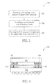
- FIG. 3 is a flowchart illustrating a method of forming a package on package (POP) structure according to a second embodiment of the present invention. Provided that substantially the same result is achieved, the steps of the flowchart shown in FIG. 3 need not be in the exact order shown and need not be contiguous; that is, other steps can be intermediate. Some steps in FIG. 3 may be omitted according to various types of embodiments or requirements.
- the method may be briefly summarized as follows:
- the POP 200 includes a first package 202 with a plurality of pillar bump pins (e.g., copper pillar bump pins 204) and a second package 206 with a plurality of pads 208, and the first package 202 and the second package 206 further connect to each other by sticking the copper pillar bump pins 204 to the pads 208 via solder.
- the first package 202 may have a memory die inside
- the second package 206 may have a logic die or another memory die inside.
- Table 2 indicates specifications of the POP 200 with different package sizes.
- Table 2 Package size Top package pitch Row/Allowable pin count 2 3 4 5 6 12mm*12mm 0.5mm 168 240 0.4mm 216 312 0.3mm 288 420 544 0.2mm 440 648 848 1041 14mm*14mm 0.5mm 200 288 0.4mm 240 372 0.3mm 344 504 656 800 0.2mm 520 768 1008 1240 1464
- FIG. 4 is a diagram illustrating a package on package (POP) structure 400 with pillar bump pins (e.g., copper pillar bump pins 404) according to a third embodiment of the present invention.
- the POP 400 includes a first package 402 with a plurality of pillar bump pins (e.g., copper pillar bump pins 404) and a second package 406 with a plurality of pads 408, and the first package 402 and the second package 406 further connect to each other by sticking the copper pillar bump pins 404 to the pads 408 via solder.
- POP package on package
- the first package 402 may have a memory die inside
- the second package 406 may have a logic die or another memory die inside.
- the difference between the second package 406 shown in FIG. 4 and the second package 206 shown in FIG. 2 is that the pad 408 of the second package 406 has leadframes while the pad 208 of the second package 206 does not have leadframes; in other words, the POP 400 is a leadframe package, and the POP 200 is a no-lead package.
- Those alternative designs concerned also belong to the scope of the present invention.
- the pillar part of the pillar bump pin may be preferably made of copper. However, this is for illustrative purposes only. In an alternative design, the pillar part of the pillar bump pin may be made of a different conductive material. To put it short, any POP structure using pillar bump pins to connect one package to another package for increasing the maximum allowable pin count falls within the scope of the present invention.
Landscapes
- Wire Bonding (AREA)
- Engineering & Computer Science (AREA)
- Manufacturing & Machinery (AREA)
- Semiconductor Memories (AREA)
Abstract
Description
- The disclosed embodiments of the present invention relate to a package on package (POP) structure, and more particularly, to a POP structure including at least a first package and a second package connected to each other via a plurality of pillar bump pins, and related method thereof.
- Package on package (POP) is a widely applied integrated circuit packaging method for combining vertically discrete logic and memory ball grid array (BGA) packages, wherein two or more packages are installed atop each other, i.e. stacked, with a standard interface to route signals between them. This allows higher component density in devices, such as mobile phones, personal digital assistants (PDA), and digital cameras.
- Configurations for POP such as pure memory stacking and mixed logic-memory stacking are commonly applied in systems having size requirements, e.g. a mobile phone. However, the conventional BGA employed for combining packages to form the POP stacking structure has its restrictions with pitch width. In other words, the pitch width of BGA is hard to be reduced and may lead to inadequate pin count between the stacked packages, which contradicts the trend of growing density of memory and logic dies.
- Therefore, one of the objectives of the present invention is to provide a POP structure including at least a first package and a second package connected to each other via a plurality of pillar bump pins and a related method thereof, to solve the aforementioned problems.
- According to one aspect of the present invention, an exemplary package on package (POP) structure is disclosed. The POP structure includes a first package and a second package. The first package has a plurality of pillar bump pins. The second package has a plurality of pads connected to the pillar bump pins, respectively.
- According to another aspect of the present invention, an exemplary method of forming a package on package (POP) structure is disclosed. The method includes: providing a first package with a plurality of pillar bump pins; providing a second package with a plurality of pads; and forming the POP structure by connecting the pillar bump pins to the pads.
- These and other objectives of the present invention will no doubt become obvious to those of ordinary skill in the art after reading the following detailed description of the preferred embodiment that is illustrated in the various figures and drawings.
-
-
FIG. 1 is a diagram illustrating a conventional package on package (POP) structure with ball grid array (BGA) pins. -
FIG. 2 is a diagram illustrating a package on package (POP) structure with pillar bump pins according to a first embodiment of the present invention. -
FIG. 3 is a flowchart illustrating a method of forming a package on package (POP) structure according to a second embodiment of the present invention. -
FIG. 4 is a diagram illustrating a package on package (POP) structure with pillar bump pins according to a third embodiment of the present invention. - Certain terms are used throughout the description and following claims to refer to particular components. As one skilled in the art will appreciate, manufacturers may refer to a component by different names. This document does not intend to distinguish between components that differ in name but not function. In the following description and in the claims, the terms "include" and "comprise" are used in an open-ended fashion, and thus should be interpreted to mean "include, but not limited to ...". Also, the term "couple" is intended to mean either an indirect or direct electrical connection. Accordingly, if one device is coupled to another device, that connection may be through a direct electrical connection, or through an indirect electrical connection via other devices and connections.
- Please refer to
FIG. 1 , which is a diagram illustrating a conventional package on package (POP)structure 100 with ball grid array (BGA)pins 104. ThePOP 100 includes afirst package 102 and asecond package 106 connected to each other via theBGA pins 104. Table 1 indicates specifications of thePOP 100 with different package sizes.Table 1 Package size Top package pitch Row Allowable pin count 12mm*12mm 0.5mm 2 168 0.4mm 2 216 14mm*14mm 0.5mm 2 200 0.4mm 2 240 - It is obvious that the allowable pin count increases as the package pitch shrinks; however, the minimum package pitch between rows of the BGA pins is 0. 4mm pursuant to its physical and electrical characteristics. Therefore, the maximum allowable BGA pin count is restricted to 216 and 240 for 12mm*12mm and 14mm*14mm POP structures, respectively.
- Please refer to
FIG. 2 in conjunction withFIG. 3 .FIG. 2 is a diagram illustrating a package on package (POP)structure 200 with pillar bump pins (e.g., copper pillar bump pins 204) according to a first embodiment of the present invention.FIG. 3 is a flowchart illustrating a method of forming a package on package (POP) structure according to a second embodiment of the present invention. Provided that substantially the same result is achieved, the steps of the flowchart shown inFIG. 3 need not be in the exact order shown and need not be contiguous; that is, other steps can be intermediate. Some steps inFIG. 3 may be omitted according to various types of embodiments or requirements. The method may be briefly summarized as follows: - Step 302: Provide a first package with a plurality of copper pillar bump pins;
- Step 304: Provide a second package with a plurality of pads; and
- Step 306: Form the POP structure by connecting the pillar bump pins to the pads.
- The
POP 200 includes afirst package 202 with a plurality of pillar bump pins (e.g., copper pillar bump pins 204) and asecond package 206 with a plurality ofpads 208, and thefirst package 202 and thesecond package 206 further connect to each other by sticking the copperpillar bump pins 204 to thepads 208 via solder. By way of example, thefirst package 202 may have a memory die inside, and thesecond package 206 may have a logic die or another memory die inside. Table 2 indicates specifications of thePOP 200 with different package sizes.Table 2 Package size Top package pitch Row/Allowable pin count 2 3 4 5 6 12mm*12mm 0.5mm 168 240 0.4mm 216 312 0.3mm 288 420 544 0.2mm 440 648 848 1041 14mm*14mm 0.5 mm 200 288 0.4mm 240 372 0.3mm 344 504 656 800 0.2mm 520 768 1008 1240 1464 - Since package pitch between rows of the copper
pillar bump pins 204 is able to be shrunk to 0.2mm pursuant to its physical and electrical characteristics, the maximum allowable pin count now extends to 1041 and 1464 for 12mm*12mm and 14mm*14mm POP structures, respectively. - It should be noted that the disclosed embodiments set forth are for illustrative purpose only, and are not meant to be limitations of the present invention. For instance, please refer to
FIG. 4 , which is a diagram illustrating a package on package (POP)structure 400 with pillar bump pins (e.g., copper pillar bump pins 404) according to a third embodiment of the present invention. ThePOP 400 includes afirst package 402 with a plurality of pillar bump pins (e.g., copper pillar bump pins 404) and asecond package 406 with a plurality ofpads 408, and thefirst package 402 and thesecond package 406 further connect to each other by sticking the copperpillar bump pins 404 to thepads 408 via solder. By way of example, thefirst package 402 may have a memory die inside, and thesecond package 406 may have a logic die or another memory die inside. The difference between thesecond package 406 shown inFIG. 4 and thesecond package 206 shown inFIG. 2 is that thepad 408 of thesecond package 406 has leadframes while thepad 208 of thesecond package 206 does not have leadframes; in other words, thePOP 400 is a leadframe package, and thePOP 200 is a no-lead package. Those alternative designs concerned also belong to the scope of the present invention. - In above embodiment, the pillar part of the pillar bump pin may be preferably made of copper. However, this is for illustrative purposes only. In an alternative design, the pillar part of the pillar bump pin may be made of a different conductive material. To put it short, any POP structure using pillar bump pins to connect one package to another package for increasing the maximum allowable pin count falls within the scope of the present invention.
- Those skilled in the art will readily observe that numerous modifications and alterations of the device and method may be made while retaining the teachings of the invention. Accordingly, the above disclosure should be construed as limited only by the metes and bounds of the appended claims.
Claims (10)
- A package on package (POP) structure, comprising:a first package, having a plurality of pillar bump pins; anda second package, having a plurality of pads connected to the pillar bump pins, respectively.
- The POP structure of claim 1, wherein the pillar bump pins are copper pillar bump pins.
- The POP structure of claim 1, wherein the first package is for a memory die.
- The POP structure of claim 1, wherein the second package is a no-lead package.
- The POP structure of claim 1, wherein the second package is a leadframe package.
- A method of forming a package on package (POP) structure, comprising:providing a first package with a plurality of pillar bump pins;providing a second package with a plurality of pads; andforming the POP structure by connecting the pillar bump pins to the pads.
- The method of claim 6, wherein the pillar bump pins are copper pillar bump pins.
- The method of claim 6, wherein the first package is for a memory die.
- The method of claim 6, wherein the second package is a no-lead package.
- The method of claim 6, wherein the second package is a leadframe package.
Applications Claiming Priority (1)
| Application Number | Priority Date | Filing Date | Title |
|---|---|---|---|
| US14/273,553 US9437577B2 (en) | 2014-05-09 | 2014-05-09 | Package on package structure with pillar bump pins and related method thereof |
Publications (1)
| Publication Number | Publication Date |
|---|---|
| EP2942810A1 true EP2942810A1 (en) | 2015-11-11 |
Family
ID=52144444
Family Applications (1)
| Application Number | Title | Priority Date | Filing Date |
|---|---|---|---|
| EP14198774.3A Withdrawn EP2942810A1 (en) | 2014-05-09 | 2014-12-18 | Package on package structure with pillar bump pins and related method thereof |
Country Status (3)
| Country | Link |
|---|---|
| US (1) | US9437577B2 (en) |
| EP (1) | EP2942810A1 (en) |
| CN (1) | CN105097745A (en) |
Families Citing this family (5)
| Publication number | Priority date | Publication date | Assignee | Title |
|---|---|---|---|---|
| CN107180801A (en) * | 2016-03-11 | 2017-09-19 | 联芯科技有限公司 | Stack assembling encapsulating structure and chip, wafer-level package chip, electronic equipment |
| DE102016206607B4 (en) * | 2016-04-19 | 2021-09-16 | Robert Bosch Gmbh | Electronic component and method for manufacturing an electronic component |
| TWI634340B (en) * | 2016-12-30 | 2018-09-01 | 友達光電股份有限公司 | Integrated circuit structure, display device module and detection method thereof |
| US10834839B1 (en) * | 2019-08-27 | 2020-11-10 | International Business Machines Corporation | Barrier for hybrid socket movement reduction |
| CN111511186A (en) * | 2020-04-24 | 2020-08-07 | 国众电子(深圳)有限公司 | Network transformer and filter assembly manufacturing method |
Citations (10)
| Publication number | Priority date | Publication date | Assignee | Title |
|---|---|---|---|---|
| US20070241463A1 (en) * | 2006-04-17 | 2007-10-18 | Elpida Memory, Inc. | Electrode, manufacturing method of the same, and semiconductor device having the same |
| US20100133665A1 (en) * | 2008-11-29 | 2010-06-03 | Jong-Woo Ha | Integrated circuit packaging system with lead frame and method of manufacture thereof |
| US20100244242A1 (en) * | 2009-03-31 | 2010-09-30 | Ibiden Co., Ltd. | Semiconductor device |
| US20110115081A1 (en) * | 2008-10-21 | 2011-05-19 | Panasonic Corporation | Multilayer semiconductor device and electronic equipment |
| US20120001306A1 (en) * | 2010-07-01 | 2012-01-05 | United Test And Assembly Center Ltd. | Semiconductor packages and methods of packaging semiconductor devices |
| US20120007232A1 (en) * | 2010-07-08 | 2012-01-12 | Tessera Research Llc | Microelectronic packages with dual or multiple-etched flip-chip connectors |
| US20120013000A1 (en) * | 2010-07-19 | 2012-01-19 | Tessera Research Llc | Stackable molded microelectronic packages |
| US20120015481A1 (en) * | 2010-07-15 | 2012-01-19 | Woo-Jae Kim | Method of manufacturing stack type semiconductor package |
| US20120193789A1 (en) * | 2011-01-27 | 2012-08-02 | Unimicron Technology Corporation | Package stack device and fabrication method thereof |
| US20130154080A1 (en) * | 2011-12-14 | 2013-06-20 | Byung Tai Do | Integrated circuit packaging system with leads and method of manufacture thereof |
Family Cites Families (15)
| Publication number | Priority date | Publication date | Assignee | Title |
|---|---|---|---|---|
| JPH01313969A (en) * | 1988-06-13 | 1989-12-19 | Hitachi Ltd | Semiconductor device |
| US7177142B2 (en) * | 2004-09-29 | 2007-02-13 | Intel Corporation | Hybrid compression socket connector for integrated circuits |
| US8120186B2 (en) * | 2008-02-15 | 2012-02-21 | Qimonda Ag | Integrated circuit and method |
| US7863732B2 (en) * | 2008-03-18 | 2011-01-04 | Stats Chippac Ltd. | Ball grid array package system |
| US8349721B2 (en) * | 2008-03-19 | 2013-01-08 | Stats Chippac, Ltd. | Semiconductor device and method of forming insulating layer on conductive traces for electrical isolation in fine pitch bonding |
| KR20100009941A (en) * | 2008-07-21 | 2010-01-29 | 삼성전자주식회사 | Semiconductor package having stepped molding compound with conductive via, method for formation of the same and stacked semiconductor package using the same |
| US8343810B2 (en) * | 2010-08-16 | 2013-01-01 | Stats Chippac, Ltd. | Semiconductor device and method of forming Fo-WLCSP having conductive layers and conductive vias separated by polymer layers |
| CN102403275B (en) * | 2010-09-17 | 2014-01-15 | 深南电路有限公司 | Package on package structure and fabricating method for same |
| US8704354B2 (en) * | 2012-03-28 | 2014-04-22 | Taiwan Semiconductor Manufacturing Company, Ltd. | Package on package structures and methods for forming the same |
| US10115671B2 (en) * | 2012-08-03 | 2018-10-30 | Snaptrack, Inc. | Incorporation of passives and fine pitch through via for package on package |
| JP5802631B2 (en) * | 2012-09-06 | 2015-10-28 | 株式会社東芝 | Semiconductor device |
| US8772950B2 (en) * | 2012-11-07 | 2014-07-08 | Taiwan Semiconductor Manufacturing Company, Ltd. | Methods and apparatus for flip chip substrate with guard rings outside of a die attach region |
| US9768142B2 (en) * | 2013-07-17 | 2017-09-19 | Taiwan Semiconductor Manufacturing Company, Ltd. | Mechanisms for forming bonding structures |
| US9508701B2 (en) * | 2013-09-27 | 2016-11-29 | Freescale Semiconductor, Inc. | 3D device packaging using through-substrate pillars |
| US9136240B2 (en) * | 2013-10-08 | 2015-09-15 | Kulicke And Soffa Industries, Inc. | Systems and methods for bonding semiconductor elements |
-
2014
- 2014-05-09 US US14/273,553 patent/US9437577B2/en active Active
- 2014-12-18 EP EP14198774.3A patent/EP2942810A1/en not_active Withdrawn
- 2014-12-18 CN CN201410790466.6A patent/CN105097745A/en active Pending
Patent Citations (10)
| Publication number | Priority date | Publication date | Assignee | Title |
|---|---|---|---|---|
| US20070241463A1 (en) * | 2006-04-17 | 2007-10-18 | Elpida Memory, Inc. | Electrode, manufacturing method of the same, and semiconductor device having the same |
| US20110115081A1 (en) * | 2008-10-21 | 2011-05-19 | Panasonic Corporation | Multilayer semiconductor device and electronic equipment |
| US20100133665A1 (en) * | 2008-11-29 | 2010-06-03 | Jong-Woo Ha | Integrated circuit packaging system with lead frame and method of manufacture thereof |
| US20100244242A1 (en) * | 2009-03-31 | 2010-09-30 | Ibiden Co., Ltd. | Semiconductor device |
| US20120001306A1 (en) * | 2010-07-01 | 2012-01-05 | United Test And Assembly Center Ltd. | Semiconductor packages and methods of packaging semiconductor devices |
| US20120007232A1 (en) * | 2010-07-08 | 2012-01-12 | Tessera Research Llc | Microelectronic packages with dual or multiple-etched flip-chip connectors |
| US20120015481A1 (en) * | 2010-07-15 | 2012-01-19 | Woo-Jae Kim | Method of manufacturing stack type semiconductor package |
| US20120013000A1 (en) * | 2010-07-19 | 2012-01-19 | Tessera Research Llc | Stackable molded microelectronic packages |
| US20120193789A1 (en) * | 2011-01-27 | 2012-08-02 | Unimicron Technology Corporation | Package stack device and fabrication method thereof |
| US20130154080A1 (en) * | 2011-12-14 | 2013-06-20 | Byung Tai Do | Integrated circuit packaging system with leads and method of manufacture thereof |
Also Published As
| Publication number | Publication date |
|---|---|
| CN105097745A (en) | 2015-11-25 |
| US20150325549A1 (en) | 2015-11-12 |
| US9437577B2 (en) | 2016-09-06 |
Similar Documents
| Publication | Publication Date | Title |
|---|---|---|
| US8053881B2 (en) | Semiconductor package and method for manufacturing the same | |
| KR102245003B1 (en) | Semiconductor packages capable of overcoming overhangs and methods for fabricating the same | |
| US8358017B2 (en) | Semiconductor package featuring flip-chip die sandwiched between metal layers | |
| US8368198B2 (en) | Stacked package of semiconductor device | |
| US20110175222A1 (en) | Semiconductor package | |
| US20040241908A1 (en) | Semiconductor package with semiconductor chips stacked therein and method of making the package | |
| CN101587868A (en) | QFN semiconductor package and method of fabricating the same | |
| US9437577B2 (en) | Package on package structure with pillar bump pins and related method thereof | |
| US20190103357A1 (en) | Methods of forming package on package assemblies with reduced z height and structures formed thereby | |
| US20130037930A1 (en) | Semiconductor chip and semiconductor package having the same | |
| KR20150021786A (en) | Semiconductor package | |
| US20090020859A1 (en) | Quad flat package with exposed common electrode bars | |
| JP4405524B2 (en) | Semiconductor device | |
| US8283757B2 (en) | Quad flat package with exposed common electrode bars | |
| US9299626B2 (en) | Die package structure | |
| US8809118B2 (en) | Chip on leads | |
| US20060289981A1 (en) | Packaging logic and memory integrated circuits | |
| KR20150045095A (en) | Interposer, method for manufacturing the same and integrated circuit package with the interposer | |
| US9601419B1 (en) | Stacked leadframe packages | |
| US20240006312A1 (en) | Barrier for minimal underfill keep-out zones | |
| US20150294957A1 (en) | Chip packaging structure | |
| KR20140092018A (en) | Semiconductor stack package having reverse interposer and a method for production thereof | |
| US20140183713A1 (en) | Die package structure | |
| CN100470782C (en) | Chip packaging structure | |
| US20220319967A1 (en) | Assembly of flexible and integrated module packages with leadframes |
Legal Events
| Date | Code | Title | Description |
|---|---|---|---|
| PUAI | Public reference made under article 153(3) epc to a published international application that has entered the european phase |
Free format text: ORIGINAL CODE: 0009012 |
|
| AK | Designated contracting states |
Kind code of ref document: A1 Designated state(s): AL AT BE BG CH CY CZ DE DK EE ES FI FR GB GR HR HU IE IS IT LI LT LU LV MC MK MT NL NO PL PT RO RS SE SI SK SM TR |
|
| AX | Request for extension of the european patent |
Extension state: BA ME |
|
| 17P | Request for examination filed |
Effective date: 20160502 |
|
| RBV | Designated contracting states (corrected) |
Designated state(s): AL AT BE BG CH CY CZ DE DK EE ES FI FR GB GR HR HU IE IS IT LI LT LU LV MC MK MT NL NO PL PT RO RS SE SI SK SM TR |
|
| 17Q | First examination report despatched |
Effective date: 20171212 |
|
| STAA | Information on the status of an ep patent application or granted ep patent |
Free format text: STATUS: THE APPLICATION IS DEEMED TO BE WITHDRAWN |
|
| 18D | Application deemed to be withdrawn |
Effective date: 20180424 |