EP2939781A1 - Machining power supply device for electric discharge machine - Google Patents
Machining power supply device for electric discharge machine Download PDFInfo
- Publication number
- EP2939781A1 EP2939781A1 EP15161566.3A EP15161566A EP2939781A1 EP 2939781 A1 EP2939781 A1 EP 2939781A1 EP 15161566 A EP15161566 A EP 15161566A EP 2939781 A1 EP2939781 A1 EP 2939781A1
- Authority
- EP
- European Patent Office
- Prior art keywords
- capacitor
- semiconductor switching
- switching element
- power supply
- machining
- Prior art date
- Legal status (The legal status is an assumption and is not a legal conclusion. Google has not performed a legal analysis and makes no representation as to the accuracy of the status listed.)
- Granted
Links
Images


Classifications
-
- B—PERFORMING OPERATIONS; TRANSPORTING
- B23—MACHINE TOOLS; METAL-WORKING NOT OTHERWISE PROVIDED FOR
- B23H—WORKING OF METAL BY THE ACTION OF A HIGH CONCENTRATION OF ELECTRIC CURRENT ON A WORKPIECE USING AN ELECTRODE WHICH TAKES THE PLACE OF A TOOL; SUCH WORKING COMBINED WITH OTHER FORMS OF WORKING OF METAL
- B23H1/00—Electrical discharge machining, i.e. removing metal with a series of rapidly recurring electrical discharges between an electrode and a workpiece in the presence of a fluid dielectric
- B23H1/02—Electric circuits specially adapted therefor, e.g. power supply, control, preventing short circuits or other abnormal discharges
- B23H1/022—Electric circuits specially adapted therefor, e.g. power supply, control, preventing short circuits or other abnormal discharges for shaping the discharge pulse train
-
- B—PERFORMING OPERATIONS; TRANSPORTING
- B23—MACHINE TOOLS; METAL-WORKING NOT OTHERWISE PROVIDED FOR
- B23H—WORKING OF METAL BY THE ACTION OF A HIGH CONCENTRATION OF ELECTRIC CURRENT ON A WORKPIECE USING AN ELECTRODE WHICH TAKES THE PLACE OF A TOOL; SUCH WORKING COMBINED WITH OTHER FORMS OF WORKING OF METAL
- B23H1/00—Electrical discharge machining, i.e. removing metal with a series of rapidly recurring electrical discharges between an electrode and a workpiece in the presence of a fluid dielectric
- B23H1/02—Electric circuits specially adapted therefor, e.g. power supply, control, preventing short circuits or other abnormal discharges
-
- B—PERFORMING OPERATIONS; TRANSPORTING
- B23—MACHINE TOOLS; METAL-WORKING NOT OTHERWISE PROVIDED FOR
- B23H—WORKING OF METAL BY THE ACTION OF A HIGH CONCENTRATION OF ELECTRIC CURRENT ON A WORKPIECE USING AN ELECTRODE WHICH TAKES THE PLACE OF A TOOL; SUCH WORKING COMBINED WITH OTHER FORMS OF WORKING OF METAL
- B23H7/00—Processes or apparatus applicable to both electrical discharge machining and electrochemical machining
- B23H7/14—Electric circuits specially adapted therefor, e.g. power supply
-
- B—PERFORMING OPERATIONS; TRANSPORTING
- B23—MACHINE TOOLS; METAL-WORKING NOT OTHERWISE PROVIDED FOR
- B23H—WORKING OF METAL BY THE ACTION OF A HIGH CONCENTRATION OF ELECTRIC CURRENT ON A WORKPIECE USING AN ELECTRODE WHICH TAKES THE PLACE OF A TOOL; SUCH WORKING COMBINED WITH OTHER FORMS OF WORKING OF METAL
- B23H2300/00—Power source circuits or energization
- B23H2300/20—Relaxation circuit power supplies for supplying the machining current, e.g. capacitor or inductance energy storage circuits
-
- B—PERFORMING OPERATIONS; TRANSPORTING
- B23—MACHINE TOOLS; METAL-WORKING NOT OTHERWISE PROVIDED FOR
- B23H—WORKING OF METAL BY THE ACTION OF A HIGH CONCENTRATION OF ELECTRIC CURRENT ON A WORKPIECE USING AN ELECTRODE WHICH TAKES THE PLACE OF A TOOL; SUCH WORKING COMBINED WITH OTHER FORMS OF WORKING OF METAL
- B23H2300/00—Power source circuits or energization
- B23H2300/20—Relaxation circuit power supplies for supplying the machining current, e.g. capacitor or inductance energy storage circuits
- B23H2300/22—Circuits using or taking into account line impedance to shape the discharge pulse
Definitions
- the present invention relates to a machining power supply device for an electric discharge machine which machines a workpiece into a desired shape by changing the relative positions of the workpiece and an electrode by a servomotor while applying a voltage to the machining gap between the electrode and the workpiece to cause an electric discharge across the gap.
- Japanese Patent Applications Laid-Open Nos. 2007-038400 and 2003-205426 discloses a method for electric discharge machining wherein a capacitor after being discharged is recharged with a voltage having the same polarity as that of the residual voltage therein, to implement a higher discharge frequency. In this method, the capacitor charging direction is not reversed.
- Japanese Patent Application Laid-Open No. 2003-205426 above discloses an electric discharge machining power supply which has a switch (field-effect transistor; FET) for short-circuiting the machining gap, to prevent a large discharge from being caused by an increased amount of charge accumulated in the gap, thereby ensuring that small discharges occur stably.
- FET field-effect transistor
- a capacitor pulsed power supply In a capacitor pulsed power supply, less variation in the charged voltage across the capacitor leads to a more constant workpiece removal amount for each pulse, ensuring more uniform surface roughness. It also leads to less variation in the gap distance of the machining gap where an electric discharge occurs, ensuring more stable machining. Further, in the case of performing electrode feed control based on an average machining-gap voltage, or, so-called voltage servo feed, the above-described variation in voltage will cause disturbance of the average machining-gap voltage, and therefore, less variation in the charged voltage is desirable. With a conventional capacitor pulsed power supply, however, the charged voltage varies widely. An attempt to suppress the variation leads to a reduced machining speed.
- FIG. 5 shows an example of a machining power supply device for an electric discharge machine equipped with a capacitor pulsed power supply.
- the machining power supply device 10 includes a DC voltage source V (voltage E), semiconductor switching elements S1 and S3, a capacitor C, a machining-gap voltage detecting unit 5 which detects a voltage across a machining gap between an electrode 2 and a workpiece 3, and a control unit 4 which turns on/off the semiconductor switching elements S1 and S3.
- FIG. 6 illustrates an operation of the machining power supply device for the electric discharge machine equipped with the capacitor pulsed power supply shown in FIG. 5 .
- the semiconductor switching element S1 is turned on for a period T1 to connect the DC voltage source V to the capacitor C for charging the capacitor C.
- the period T1 which is set in advance, is a time sufficient for the capacitor C to be charged.
- the semiconductor switching element S1 is turned off and, at the same time, the semiconductor switching element S3 is turned on to connect the charged capacitor C in parallel with the machining gap between the electrode and the workpiece.
- the gap between the electrode and the workpiece is sufficiently small, an electric discharge occurs at a certain time point, and the charge accumulated in the capacitor C is discharged to the machining gap, whereby removal processing of the workpiece 3 is carried out.
- the machining-gap voltage detecting unit 5 checks for the occurrence of electric discharge, and upon detection of an electric discharge, the semiconductor switching element S3 is kept on for a period T2 from the time point when the discharge was detected. It may be configured such that a machining-gap current Ig is detected by a detecting unit (not shown).
- the machining-gap voltage is denoted by Vg.
- the period T2 is a time sufficient for the capacitor C to be fully discharged. At this time, the capacitor C is charged in the direction opposite to the direction in which it was originally charged. This voltage (residual voltage) in the opposite direction varies depending on the state of the machining gap. Thereafter, a quiescent period is provided for a period T3 for recovery of insulation between the electrode and the workpiece. The above completes one cycle.
- the charged voltage jumps to exceed the power supply voltage E, as shown in FIG. 6 .
- the amount of the jump depends on the residual voltage in the opposite direction. That is, the voltage jumps higher with a greater residual voltage (absolute value thereof).
- the above-described mechanism causes the charged voltage across the capacitor C to vary.
- an object of the present invention is to provide a machining power supply device for an electric discharge machine capable of preventing variation in the charged voltage across a capacitor, without causing reduction of the machining speed.
- a machining power supply device for an electric discharge machine is for an electric discharge machine configured to machine a workpiece by applying a voltage to a machining gap between an electrode and the workpiece to cause an electric discharge across the gap.
- the machining power supply device includes: a DC power supply; a capacitor directly or indirectly connected in parallel with the machining gap; a first semiconductor switching element arranged in series between the DC power supply and the capacitor; a second semiconductor switching element arranged in parallel with the capacitor; a rectifier element inserted in a circuit loop composed of the capacitor and the second semiconductor switching element; and a control unit configured to control the first and the second semiconductor switching elements, wherein the control unit is configured to turn on the first semiconductor switching element to charge the capacitor, and turn on the second semiconductor switching element within a period in which the first semiconductor switching element is off.
- the machining power supply device for an electric discharge machine configured to machine a workpiece by applying a voltage to a machining gap between an electrode and the workpiece to cause an electric discharge across the gap.
- the machining power supply device includes: a DC power supply; a capacitor directly or indirectly connected in parallel with the machining gap; a first semiconductor switching element arranged in series between the DC power supply and the capacitor; a second semiconductor switching element arranged in parallel with the capacitor; a detecting unit configured to detect a voltage or a current of the capacitor; and a control unit configured to control the first and the second semiconductor switching elements, wherein the control unit is configured to turn on the first semiconductor switching element to charge the capacitor, turn on the second semiconductor switching element within a period in which the first semiconductor switching element is off, and turn off the second semiconductor switching element in accordance with a detected value of the voltage or the current of the capacitor.
- the above machining power supply devices may each include a third semiconductor switching element arranged in series between the machining gap and the capacitor, and the control unit may further perform control to turn on the third semiconductor switching element when turning off the first semiconductor switching element, and turn on the second semiconductor switching element within a period in which the first semiconductor switching element and the third semiconductor switching element are both off.
- the present invention can provide the machining power supply devices for an electric discharge machine capable of preventing variation in the charged voltage across the capacitor, without causing reduction of the machining speed.
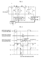
- FIG. 1 shows an embodiment of a machining power supply device for an electric discharge machine according to the present invention.
- the electric discharge machine include a wire electric discharge machine and a die sinking electric discharge machine.
- the machining power supply device 1 is a power supply device for an electric discharge machine which performs electric discharge machining of a workpiece 3 by applying a voltage to a machining gap between an electrode 2 and the workpiece 3.
- the machining power supply device 1 for the electric discharge machine includes a DC voltage source V (voltage E), a first semiconductor switching element S1, a second semiconductor switching element S2, a third semiconductor switching element S3, a capacitor C, a rectifier element D, a machining-gap voltage detecting unit 5, and a control unit 4 which turns on/off the first and third semiconductor switching elements S1 and S3.
- V DC voltage source
- L1 L2, and L3 denote stray inductances.
- the capacitor C is charged by the DC voltage source V.
- the electric power charged in the capacitor C is applied in pulses to the machining gap between the electrode 2 and the workpiece 3.
- the machining-gap voltage detecting unit 5 detects the voltage across the machining gap.
- a machining-gap current Ig flowing across the machining gap may be detected by a detecting unit.
- FIG. 2 illustrates an operation of the machining power supply device 1 for the electric discharge machine in the case of using the capacitor pulsed power supply in FIG. 1 .
- the first semiconductor switching element S1 is turned on for a period T1 to connect the DC voltage source V to the capacitor C for charging the capacitor C.
- the period T1 which is set in advance, is a time sufficient for the capacitor C to be charged.
- the first semiconductor switching element S1 is turned off and, at the same time, the third semiconductor switching element S3 is turned on to connect the charged capacitor C in parallel with the machining gap between the electrode 2 and the workpiece 3.
- an electric discharge occurs at a certain time point, and the charge accumulated in the capacitor C is discharged to the machining gap, whereby the removal machining of the workpiece 3 is carried out.
- the machining-gap voltage detecting unit 5 checks for the occurrence of electric discharge, and upon detection of an electric discharge, the third semiconductor switching element S3 is kept on for a period T2 from the time point when the discharge was detected.
- the period T2 is a time sufficient for the capacitor C to be fully discharged.
- the capacitor C is charged in the direction opposite to the direction in which it was originally charged.
- a quiescent period is provided for a period T3.
- the second semiconductor switching element S2 is turned on within a period (period T4 in FIG. 2 ) in which the first semiconductor switching element S1 is off, to reverse the residual voltage in the opposite direction.
- the rectifier element D is inserted in the direction in which it can reverse the residual voltage charged in the opposite direction.
- the rectifier element D serves to prevent the voltage that has been once reversed from being reversed again. The above completes one cycle.
- the first semiconductor switching element S1 is turned on again in the next cycle to charge the capacitor C, the charged voltage will not jump; rather, it will become approximately equal to the power supply voltage E.
- This embodiment differs from the embodiment shown in FIG. 1 in that the rectifier element D is replaced with a capacitor voltage detecting unit 6 which detects the voltage of the capacitor C.
- the control unit 4 With the voltage of the capacitor C (capacitor voltage Vc) being monitored by the capacitor voltage detecting unit 6, when the voltage attains a desired value (which is zero in the example in FIG. 4 ), the control unit 4 turns off the second semiconductor switching element S2, to thereby control the residual voltage of the capacitor C.
- the current flowing through the capacitor C is detected by a detecting unit (not shown).
- the control unit 4 may turn off the second semiconductor switching element S2 on the basis of the detected current value, to control the residual voltage of the capacitor C.
- the charged voltage can be controlled to take a desired value (which is zero, or may be a reduced value if not reversed). In this embodiment as well, it is possible to suppress the variation in the charged voltage across the capacitor.
Landscapes
- Engineering & Computer Science (AREA)
- Mechanical Engineering (AREA)
- Chemical & Material Sciences (AREA)
- Chemical Kinetics & Catalysis (AREA)
- Electrochemistry (AREA)
- Electrical Discharge Machining, Electrochemical Machining, And Combined Machining (AREA)
- Generation Of Surge Voltage And Current (AREA)
Abstract
Description
- The present invention relates to a machining power supply device for an electric discharge machine which machines a workpiece into a desired shape by changing the relative positions of the workpiece and an electrode by a servomotor while applying a voltage to the machining gap between the electrode and the workpiece to cause an electric discharge across the gap.
- In electric discharge machining, rough machining and finish machining are used for different purposes. In the rough machining, the energy of a single discharge is increased to do high-speed processing. In the finish machining, the energy of a single discharge is decreased to do high-precision processing. For the finish machining, a "capacitor pulsed power supply" is widely used in which the charged energy in the capacitor is utilized for machining.
- Techniques related to a machining power supply device for an electric discharge machine equipped with a capacitor pulsed power supply are disclosed in Japanese Patent Applications Laid-Open Nos.
2007-038400 2003-205426 2007-038400 - Japanese Patent Application Laid-Open No.
2003-205426 - In a capacitor pulsed power supply, less variation in the charged voltage across the capacitor leads to a more constant workpiece removal amount for each pulse, ensuring more uniform surface roughness. It also leads to less variation in the gap distance of the machining gap where an electric discharge occurs, ensuring more stable machining. Further, in the case of performing electrode feed control based on an average machining-gap voltage, or, so-called voltage servo feed, the above-described variation in voltage will cause disturbance of the average machining-gap voltage, and therefore, less variation in the charged voltage is desirable. With a conventional capacitor pulsed power supply, however, the charged voltage varies widely. An attempt to suppress the variation leads to a reduced machining speed.
-
FIG. 5 shows an example of a machining power supply device for an electric discharge machine equipped with a capacitor pulsed power supply. - The machining
power supply device 10 includes a DC voltage source V (voltage E), semiconductor switching elements S1 and S3, a capacitor C, a machining-gapvoltage detecting unit 5 which detects a voltage across a machining gap between anelectrode 2 and aworkpiece 3, and acontrol unit 4 which turns on/off the semiconductor switching elements S1 and S3. -
FIG. 6 illustrates an operation of the machining power supply device for the electric discharge machine equipped with the capacitor pulsed power supply shown inFIG. 5 . First, at the beginning of a cycle, the semiconductor switching element S1 is turned on for a period T1 to connect the DC voltage source V to the capacitor C for charging the capacitor C. The period T1, which is set in advance, is a time sufficient for the capacitor C to be charged. - Next, the semiconductor switching element S1 is turned off and, at the same time, the semiconductor switching element S3 is turned on to connect the charged capacitor C in parallel with the machining gap between the electrode and the workpiece. When the gap between the electrode and the workpiece is sufficiently small, an electric discharge occurs at a certain time point, and the charge accumulated in the capacitor C is discharged to the machining gap, whereby removal processing of the
workpiece 3 is carried out. - Here, the machining-gap
voltage detecting unit 5 checks for the occurrence of electric discharge, and upon detection of an electric discharge, the semiconductor switching element S3 is kept on for a period T2 from the time point when the discharge was detected. It may be configured such that a machining-gap current Ig is detected by a detecting unit (not shown). Here, the machining-gap voltage is denoted by Vg. The period T2 is a time sufficient for the capacitor C to be fully discharged. At this time, the capacitor C is charged in the direction opposite to the direction in which it was originally charged. This voltage (residual voltage) in the opposite direction varies depending on the state of the machining gap. Thereafter, a quiescent period is provided for a period T3 for recovery of insulation between the electrode and the workpiece. The above completes one cycle. - In the case where the semiconductor switching element S1 is turned on again in the next cycle to charge the capacitor C, the charged voltage jumps to exceed the power supply voltage E, as shown in
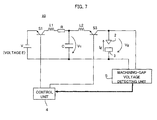
FIG. 6 . The amount of the jump depends on the residual voltage in the opposite direction. That is, the voltage jumps higher with a greater residual voltage (absolute value thereof). The above-described mechanism causes the charged voltage across the capacitor C to vary. - One of the most reliable ways of suppressing the variation in the charged voltage across the capacitor C will be to insert a current limiting resistor R in the charging circuit for the capacitor C (see
FIG. 7 ). Even if the capacitor C is charged in the direction opposite to the direction in which it was originally charged, when the capacitor C is charged in a next cycle, the current limiting resistor R plays a damping role, so the variation in the charged voltage across the capacitor C can be prevented. - This approach, however, increases the time taken for charging the capacitor C, leading to reduction of the machining speed.
- In view of the above-described problems of the conventional techniques, an object of the present invention is to provide a machining power supply device for an electric discharge machine capable of preventing variation in the charged voltage across a capacitor, without causing reduction of the machining speed.
- A machining power supply device for an electric discharge machine according to the present invention is for an electric discharge machine configured to machine a workpiece by applying a voltage to a machining gap between an electrode and the workpiece to cause an electric discharge across the gap. The machining power supply device includes: a DC power supply; a capacitor directly or indirectly connected in parallel with the machining gap; a first semiconductor switching element arranged in series between the DC power supply and the capacitor; a second semiconductor switching element arranged in parallel with the capacitor; a rectifier element inserted in a circuit loop composed of the capacitor and the second semiconductor switching element; and a control unit configured to control the first and the second semiconductor switching elements, wherein the control unit is configured to turn on the first semiconductor switching element to charge the capacitor, and turn on the second semiconductor switching element within a period in which the first semiconductor switching element is off.
- Another machining power supply device for an electric discharge machine according to the present invention is for an electric discharge machine configured to machine a workpiece by applying a voltage to a machining gap between an electrode and the workpiece to cause an electric discharge across the gap. The machining power supply device includes: a DC power supply; a capacitor directly or indirectly connected in parallel with the machining gap; a first semiconductor switching element arranged in series between the DC power supply and the capacitor; a second semiconductor switching element arranged in parallel with the capacitor; a detecting unit configured to detect a voltage or a current of the capacitor; and a control unit configured to control the first and the second semiconductor switching elements, wherein the control unit is configured to turn on the first semiconductor switching element to charge the capacitor, turn on the second semiconductor switching element within a period in which the first semiconductor switching element is off, and turn off the second semiconductor switching element in accordance with a detected value of the voltage or the current of the capacitor.
- The above machining power supply devices may each include a third semiconductor switching element arranged in series between the machining gap and the capacitor, and the control unit may further perform control to turn on the third semiconductor switching element when turning off the first semiconductor switching element, and turn on the second semiconductor switching element within a period in which the first semiconductor switching element and the third semiconductor switching element are both off.
- With the above-described configurations, the present invention can provide the machining power supply devices for an electric discharge machine capable of preventing variation in the charged voltage across the capacitor, without causing reduction of the machining speed.
- The above and other objects and features of the present invention will be obvious from the ensuing description of embodiments with reference to the accompanying drawings, in which:
-
FIG. 1 shows an embodiment of a machining power supply device for an electric discharge machine according to the present invention; -
FIG. 2 illustrates an operation of the machining power supply device for the electric discharge machine in the case of using the capacitor pulsed power supply inFIG. 1 ; -
FIG. 3 shows another embodiment of the present invention; -
FIG. 4 illustrates an operation of the machining power supply device for the electric discharge machine in the case of using the capacitor pulsed power supply inFIG. 3 ; -
FIG. 5 shows an example of a machining power supply device for an electric discharge machine including a conventional capacitor pulsed power supply; -
FIG. 6 illustrates an operation of the machining power supply device for the electric discharge machine in the case of using the capacitor pulsed power supply inFIG. 5 ; and -
FIG. 7 shows another example of the capacitor pulsed power supply. - Hereinafter, the same or similar components and structures as those in the conventional techniques are denoted by the same reference characters.
-
FIG. 1 shows an embodiment of a machining power supply device for an electric discharge machine according to the present invention. Examples of the electric discharge machine include a wire electric discharge machine and a die sinking electric discharge machine. The machiningpower supply device 1 is a power supply device for an electric discharge machine which performs electric discharge machining of aworkpiece 3 by applying a voltage to a machining gap between anelectrode 2 and theworkpiece 3. The machiningpower supply device 1 for the electric discharge machine includes a DC voltage source V (voltage E), a first semiconductor switching element S1, a second semiconductor switching element S2, a third semiconductor switching element S3, a capacitor C, a rectifier element D, a machining-gapvoltage detecting unit 5, and acontrol unit 4 which turns on/off the first and third semiconductor switching elements S1 and S3. In the figure, reference characters L1, L2, and L3 denote stray inductances. The capacitor C is charged by the DC voltage source V. The electric power charged in the capacitor C is applied in pulses to the machining gap between theelectrode 2 and theworkpiece 3. The machining-gapvoltage detecting unit 5 detects the voltage across the machining gap. Although not shown in the figure, a machining-gap current Ig flowing across the machining gap may be detected by a detecting unit. -
FIG. 2 illustrates an operation of the machiningpower supply device 1 for the electric discharge machine in the case of using the capacitor pulsed power supply inFIG. 1 . First, at the beginning of a cycle, the first semiconductor switching element S1 is turned on for a period T1 to connect the DC voltage source V to the capacitor C for charging the capacitor C. The period T1, which is set in advance, is a time sufficient for the capacitor C to be charged. The first semiconductor switching element S1 is turned off and, at the same time, the third semiconductor switching element S3 is turned on to connect the charged capacitor C in parallel with the machining gap between theelectrode 2 and theworkpiece 3. When the gap between the electrode and the workpiece is sufficiently small, an electric discharge occurs at a certain time point, and the charge accumulated in the capacitor C is discharged to the machining gap, whereby the removal machining of theworkpiece 3 is carried out. - Here, the machining-gap
voltage detecting unit 5 checks for the occurrence of electric discharge, and upon detection of an electric discharge, the third semiconductor switching element S3 is kept on for a period T2 from the time point when the discharge was detected. The period T2 is a time sufficient for the capacitor C to be fully discharged. At this time, the capacitor C is charged in the direction opposite to the direction in which it was originally charged. Thereafter, a quiescent period is provided for a period T3. During the period T3, the second semiconductor switching element S2 is turned on within a period (period T4 inFIG. 2 ) in which the first semiconductor switching element S1 is off, to reverse the residual voltage in the opposite direction. - Here, the rectifier element D is inserted in the direction in which it can reverse the residual voltage charged in the opposite direction. The rectifier element D serves to prevent the voltage that has been once reversed from being reversed again. The above completes one cycle. When the first semiconductor switching element S1 is turned on again in the next cycle to charge the capacitor C, the charged voltage will not jump; rather, it will become approximately equal to the power supply voltage E.
- Another embodiment will be described with reference to
FIG. 3 . - This embodiment differs from the embodiment shown in
FIG. 1 in that the rectifier element D is replaced with a capacitor voltage detecting unit 6 which detects the voltage of the capacitor C. With the voltage of the capacitor C (capacitor voltage Vc) being monitored by the capacitor voltage detecting unit 6, when the voltage attains a desired value (which is zero in the example inFIG. 4 ), thecontrol unit 4 turns off the second semiconductor switching element S2, to thereby control the residual voltage of the capacitor C. It should be noted that the current flowing through the capacitor C is detected by a detecting unit (not shown). Thecontrol unit 4 may turn off the second semiconductor switching element S2 on the basis of the detected current value, to control the residual voltage of the capacitor C. - While the residual voltage is reversed in the embodiment shown in
FIG. 1 , in the embodiment shown inFIG. 3 , the charged voltage can be controlled to take a desired value (which is zero, or may be a reduced value if not reversed). In this embodiment as well, it is possible to suppress the variation in the charged voltage across the capacitor.
Claims (3)
- A machining power supply device for an electric discharge machine configured to machine a workpiece by applying a voltage to a machining gap between an electrode and the workpiece to cause an electric discharge across the gap, the machining power supply device comprising:a DC power supply;a capacitor directly or indirectly connected in parallel with the machining gap;a first semiconductor switching element arranged in series between the DC power supply and the capacitor;a second semiconductor switching element arranged in parallel with the capacitor;a rectifier element inserted in a circuit loop composed of the capacitor and the second semiconductor switching element; anda control unit configured to control the first and the second semiconductor switching elements, whereinthe control unit is configured to turn on the first semiconductor switching element to charge the capacitor, and turn on the second semiconductor switching element within a period in which the first semiconductor switching element is off.
- A machining power supply device for an electric discharge machine configured to machine a workpiece by applying a voltage to a machining gap between an electrode and the workpiece to cause an electric discharge across the gap, the machining power supply device comprising:a DC power supply;a capacitor directly or indirectly connected in parallel with the machining gap;a first semiconductor switching element arranged in series between the DC power supply and the capacitor;a second semiconductor switching element arranged in parallel with the capacitor;a detecting unit configured to detect a voltage or a current of the capacitor; anda control unit configured to control the first and the second semiconductor switching elements, whereinthe control unit is configured to turn on the first semiconductor switching element to charge the capacitor, turn on the second semiconductor switching element within a period in which the first semiconductor switching element is off, and turn off the second semiconductor switching element in accordance with a detected value of the voltage or the current of the capacitor.
- The machining power supply device for the electric discharge machine according to claim 1 or 2, further comprising a third semiconductor switching element arranged in series between the machining gap and the capacitor, wherein the control unit is further configured to
turn on the third semiconductor switching element when turning off the first semiconductor switching element, and
turn on the second semiconductor switching element within a period in which the first semiconductor switching element and the third semiconductor switching element are both off.
Priority Applications (1)
| Application Number | Priority Date | Filing Date | Title |
|---|---|---|---|
| EP19171308.0A EP3566805B1 (en) | 2014-04-30 | 2015-03-30 | Machining power supply device for electric discharge machine |
Applications Claiming Priority (1)
| Application Number | Priority Date | Filing Date | Title |
|---|---|---|---|
| JP2014094293A JP5887378B2 (en) | 2014-04-30 | 2014-04-30 | Machining power supply device for electrical discharge machine |
Related Child Applications (2)
| Application Number | Title | Priority Date | Filing Date |
|---|---|---|---|
| EP19171308.0A Division-Into EP3566805B1 (en) | 2014-04-30 | 2015-03-30 | Machining power supply device for electric discharge machine |
| EP19171308.0A Division EP3566805B1 (en) | 2014-04-30 | 2015-03-30 | Machining power supply device for electric discharge machine |
Publications (2)
| Publication Number | Publication Date |
|---|---|
| EP2939781A1 true EP2939781A1 (en) | 2015-11-04 |
| EP2939781B1 EP2939781B1 (en) | 2019-09-11 |
Family
ID=52774150
Family Applications (2)
| Application Number | Title | Priority Date | Filing Date |
|---|---|---|---|
| EP15161566.3A Active EP2939781B1 (en) | 2014-04-30 | 2015-03-30 | Machining power supply device for electric discharge machine |
| EP19171308.0A Active EP3566805B1 (en) | 2014-04-30 | 2015-03-30 | Machining power supply device for electric discharge machine |
Family Applications After (1)
| Application Number | Title | Priority Date | Filing Date |
|---|---|---|---|
| EP19171308.0A Active EP3566805B1 (en) | 2014-04-30 | 2015-03-30 | Machining power supply device for electric discharge machine |
Country Status (4)
| Country | Link |
|---|---|
| US (1) | US10220458B2 (en) |
| EP (2) | EP2939781B1 (en) |
| JP (1) | JP5887378B2 (en) |
| CN (1) | CN105033369B (en) |
Cited By (2)
| Publication number | Priority date | Publication date | Assignee | Title |
|---|---|---|---|---|
| CN113857594A (en) * | 2021-09-28 | 2021-12-31 | 南京理工大学 | Grouping type micro electric spark machining pulse power supply |
| CN114237079A (en) * | 2021-09-30 | 2022-03-25 | 宁波三星智能电气有限公司 | Circuit capable of utilizing serial port to turn off power supply |
Families Citing this family (2)
| Publication number | Priority date | Publication date | Assignee | Title |
|---|---|---|---|---|
| JP6770041B2 (en) * | 2018-10-23 | 2020-10-14 | ファナック株式会社 | Wire electric discharge machine and electric discharge machining method |
| JP7311366B2 (en) * | 2019-09-09 | 2023-07-19 | ファナック株式会社 | Wire electric discharge machine and control method |
Citations (4)
| Publication number | Priority date | Publication date | Assignee | Title |
|---|---|---|---|---|
| JPS58196923A (en) * | 1982-05-10 | 1983-11-16 | Mitsubishi Electric Corp | Power source device for discharge machining |
| US6580048B2 (en) * | 2000-12-01 | 2003-06-17 | Mitsubishi Denki Kabushiki Kaisha | Electrical discharge machining apparatus supplying initial and processing currents |
| JP2003205426A (en) | 2001-11-06 | 2003-07-22 | Mitsubishi Electric Corp | Power supply for electric discharge machine |
| JP2007038400A (en) | 2005-08-01 | 2007-02-15 | Agie Sa | Method and generator for electrical discharge machining |
Family Cites Families (10)
| Publication number | Priority date | Publication date | Assignee | Title |
|---|---|---|---|---|
| JPS5656341A (en) * | 1979-10-05 | 1981-05-18 | Fanuc Ltd | Power source for wire cut electric discharge machining |
| JPS632611A (en) * | 1986-06-18 | 1988-01-07 | Fanuc Ltd | Electric discharge machining power source |
| JP2590150B2 (en) * | 1987-11-30 | 1997-03-12 | 株式会社放電精密加工研究所 | Power supply circuit for electric discharge machining |
| JPH06143034A (en) * | 1992-11-06 | 1994-05-24 | Fanuc Ltd | Electric discharge machining method and device |
| JP2005246551A (en) | 2004-03-04 | 2005-09-15 | Fanuc Ltd | Power supply apparatus for electric discharge machining |
| JP4833198B2 (en) * | 2006-10-20 | 2011-12-07 | 三菱電機株式会社 | Power control device for electrical discharge machine |
| US8420973B2 (en) * | 2006-10-20 | 2013-04-16 | Mitsubishi Electric Corporation | Power-supply control device for electrical discharge machining apparatus |
| WO2008050403A1 (en) * | 2006-10-24 | 2008-05-02 | Mitsubishi Electric Corporation | Wire discharge processing apparatus |
| US8093526B2 (en) * | 2006-10-24 | 2012-01-10 | Mitsubishi Electric Corporation | Wire electric discharge machine with impedance switching |
| DE112012007077B4 (en) * | 2012-10-31 | 2021-12-09 | Mitsubishi Electric Corporation | Electric discharge machining device |
-
2014
- 2014-04-30 JP JP2014094293A patent/JP5887378B2/en active Active
-
2015
- 2015-03-30 EP EP15161566.3A patent/EP2939781B1/en active Active
- 2015-03-30 EP EP19171308.0A patent/EP3566805B1/en active Active
- 2015-04-23 US US14/694,501 patent/US10220458B2/en active Active
- 2015-04-29 CN CN201510212619.3A patent/CN105033369B/en active Active
Patent Citations (4)
| Publication number | Priority date | Publication date | Assignee | Title |
|---|---|---|---|---|
| JPS58196923A (en) * | 1982-05-10 | 1983-11-16 | Mitsubishi Electric Corp | Power source device for discharge machining |
| US6580048B2 (en) * | 2000-12-01 | 2003-06-17 | Mitsubishi Denki Kabushiki Kaisha | Electrical discharge machining apparatus supplying initial and processing currents |
| JP2003205426A (en) | 2001-11-06 | 2003-07-22 | Mitsubishi Electric Corp | Power supply for electric discharge machine |
| JP2007038400A (en) | 2005-08-01 | 2007-02-15 | Agie Sa | Method and generator for electrical discharge machining |
Cited By (3)
| Publication number | Priority date | Publication date | Assignee | Title |
|---|---|---|---|---|
| CN113857594A (en) * | 2021-09-28 | 2021-12-31 | 南京理工大学 | Grouping type micro electric spark machining pulse power supply |
| CN114237079A (en) * | 2021-09-30 | 2022-03-25 | 宁波三星智能电气有限公司 | Circuit capable of utilizing serial port to turn off power supply |
| CN114237079B (en) * | 2021-09-30 | 2024-04-30 | 宁波三星智能电气有限公司 | Circuit capable of utilizing serial port to turn off power supply |
Also Published As
| Publication number | Publication date |
|---|---|
| US10220458B2 (en) | 2019-03-05 |
| EP2939781B1 (en) | 2019-09-11 |
| US20150314383A1 (en) | 2015-11-05 |
| JP5887378B2 (en) | 2016-03-16 |
| CN105033369B (en) | 2018-02-16 |
| EP3566805A1 (en) | 2019-11-13 |
| JP2015208846A (en) | 2015-11-24 |
| EP3566805B1 (en) | 2023-01-25 |
| CN105033369A (en) | 2015-11-11 |
Similar Documents
| Publication | Publication Date | Title |
|---|---|---|
| JP5739563B2 (en) | Wire electric discharge machine equipped with means for calculating average discharge delay time | |
| US10730126B2 (en) | Power supply device for wire electric discharge machining | |
| EP3566805B1 (en) | Machining power supply device for electric discharge machine | |
| EP3812073B1 (en) | Wire electrical discharge machine and control method | |
| US9815132B2 (en) | Wire electric discharge machine | |
| US4357516A (en) | EDM Method and apparatus utilizing successive trains of elementary pulses with controlled pulse-off periods | |
| JP5800923B2 (en) | Power supply device for wire electric discharge machine | |
| EP3643440B1 (en) | Wire electrical discharge machine and electrical discharge machining method | |
| JP5372095B2 (en) | EDM machine | |
| JP2017061023A (en) | Machining power supply of wire electric discharge machine | |
| JP6230481B2 (en) | Multi-wire electric discharge machine | |
| JP2013184255A (en) | Discharge control method for small hole electric discharge machine and power supply device for small hole electrical discharge machining | |
| JP4425056B2 (en) | EDM power supply | |
| JP2002154015A (en) | Contact detecting device for electric discharge machine | |
| JP5940229B1 (en) | EDM power supply | |
| JPH0329530B2 (en) | ||
| JP2005297164A (en) | EDM machine | |
| JP2009066756A (en) | EDM machine | |
| JPH0724637A (en) | Electric power unit for electric discharge machining | |
| JPS61100317A (en) | Electric discharge machining device |
Legal Events
| Date | Code | Title | Description |
|---|---|---|---|
| PUAI | Public reference made under article 153(3) epc to a published international application that has entered the european phase |
Free format text: ORIGINAL CODE: 0009012 |
|
| AK | Designated contracting states |
Kind code of ref document: A1 Designated state(s): AL AT BE BG CH CY CZ DE DK EE ES FI FR GB GR HR HU IE IS IT LI LT LU LV MC MK MT NL NO PL PT RO RS SE SI SK SM TR |
|
| AX | Request for extension of the european patent |
Extension state: BA ME |
|
| 17P | Request for examination filed |
Effective date: 20160504 |
|
| RBV | Designated contracting states (corrected) |
Designated state(s): AL AT BE BG CH CY CZ DE DK EE ES FI FR GB GR HR HU IE IS IT LI LT LU LV MC MK MT NL NO PL PT RO RS SE SI SK SM TR |
|
| STAA | Information on the status of an ep patent application or granted ep patent |
Free format text: STATUS: EXAMINATION IS IN PROGRESS |
|
| 17Q | First examination report despatched |
Effective date: 20180409 |
|
| GRAP | Despatch of communication of intention to grant a patent |
Free format text: ORIGINAL CODE: EPIDOSNIGR1 |
|
| STAA | Information on the status of an ep patent application or granted ep patent |
Free format text: STATUS: GRANT OF PATENT IS INTENDED |
|
| INTG | Intention to grant announced |
Effective date: 20190618 |
|
| GRAS | Grant fee paid |
Free format text: ORIGINAL CODE: EPIDOSNIGR3 |
|
| GRAA | (expected) grant |
Free format text: ORIGINAL CODE: 0009210 |
|
| STAA | Information on the status of an ep patent application or granted ep patent |
Free format text: STATUS: THE PATENT HAS BEEN GRANTED |
|
| AK | Designated contracting states |
Kind code of ref document: B1 Designated state(s): AL AT BE BG CH CY CZ DE DK EE ES FI FR GB GR HR HU IE IS IT LI LT LU LV MC MK MT NL NO PL PT RO RS SE SI SK SM TR |
|
| REG | Reference to a national code |
Ref country code: GB Ref legal event code: FG4D |
|
| REG | Reference to a national code |
Ref country code: CH Ref legal event code: EP |
|
| REG | Reference to a national code |
Ref country code: AT Ref legal event code: REF Ref document number: 1177804 Country of ref document: AT Kind code of ref document: T Effective date: 20190915 |
|
| REG | Reference to a national code |
Ref country code: DE Ref legal event code: R096 Ref document number: 602015037605 Country of ref document: DE Ref country code: IE Ref legal event code: FG4D |
|
| REG | Reference to a national code |
Ref country code: NL Ref legal event code: MP Effective date: 20190911 |
|
| REG | Reference to a national code |
Ref country code: LT Ref legal event code: MG4D |
|
| PG25 | Lapsed in a contracting state [announced via postgrant information from national office to epo] |
Ref country code: BG Free format text: LAPSE BECAUSE OF FAILURE TO SUBMIT A TRANSLATION OF THE DESCRIPTION OR TO PAY THE FEE WITHIN THE PRESCRIBED TIME-LIMIT Effective date: 20191211 Ref country code: NO Free format text: LAPSE BECAUSE OF FAILURE TO SUBMIT A TRANSLATION OF THE DESCRIPTION OR TO PAY THE FEE WITHIN THE PRESCRIBED TIME-LIMIT Effective date: 20191211 Ref country code: FI Free format text: LAPSE BECAUSE OF FAILURE TO SUBMIT A TRANSLATION OF THE DESCRIPTION OR TO PAY THE FEE WITHIN THE PRESCRIBED TIME-LIMIT Effective date: 20190911 Ref country code: LT Free format text: LAPSE BECAUSE OF FAILURE TO SUBMIT A TRANSLATION OF THE DESCRIPTION OR TO PAY THE FEE WITHIN THE PRESCRIBED TIME-LIMIT Effective date: 20190911 Ref country code: SE Free format text: LAPSE BECAUSE OF FAILURE TO SUBMIT A TRANSLATION OF THE DESCRIPTION OR TO PAY THE FEE WITHIN THE PRESCRIBED TIME-LIMIT Effective date: 20190911 Ref country code: HR Free format text: LAPSE BECAUSE OF FAILURE TO SUBMIT A TRANSLATION OF THE DESCRIPTION OR TO PAY THE FEE WITHIN THE PRESCRIBED TIME-LIMIT Effective date: 20190911 |
|
| PG25 | Lapsed in a contracting state [announced via postgrant information from national office to epo] |
Ref country code: AL Free format text: LAPSE BECAUSE OF FAILURE TO SUBMIT A TRANSLATION OF THE DESCRIPTION OR TO PAY THE FEE WITHIN THE PRESCRIBED TIME-LIMIT Effective date: 20190911 Ref country code: LV Free format text: LAPSE BECAUSE OF FAILURE TO SUBMIT A TRANSLATION OF THE DESCRIPTION OR TO PAY THE FEE WITHIN THE PRESCRIBED TIME-LIMIT Effective date: 20190911 Ref country code: GR Free format text: LAPSE BECAUSE OF FAILURE TO SUBMIT A TRANSLATION OF THE DESCRIPTION OR TO PAY THE FEE WITHIN THE PRESCRIBED TIME-LIMIT Effective date: 20191212 Ref country code: RS Free format text: LAPSE BECAUSE OF FAILURE TO SUBMIT A TRANSLATION OF THE DESCRIPTION OR TO PAY THE FEE WITHIN THE PRESCRIBED TIME-LIMIT Effective date: 20190911 Ref country code: ES Free format text: LAPSE BECAUSE OF FAILURE TO SUBMIT A TRANSLATION OF THE DESCRIPTION OR TO PAY THE FEE WITHIN THE PRESCRIBED TIME-LIMIT Effective date: 20190911 |
|
| REG | Reference to a national code |
Ref country code: AT Ref legal event code: MK05 Ref document number: 1177804 Country of ref document: AT Kind code of ref document: T Effective date: 20190911 |
|
| PG25 | Lapsed in a contracting state [announced via postgrant information from national office to epo] |
Ref country code: PT Free format text: LAPSE BECAUSE OF FAILURE TO SUBMIT A TRANSLATION OF THE DESCRIPTION OR TO PAY THE FEE WITHIN THE PRESCRIBED TIME-LIMIT Effective date: 20200113 Ref country code: IT Free format text: LAPSE BECAUSE OF FAILURE TO SUBMIT A TRANSLATION OF THE DESCRIPTION OR TO PAY THE FEE WITHIN THE PRESCRIBED TIME-LIMIT Effective date: 20190911 Ref country code: AT Free format text: LAPSE BECAUSE OF FAILURE TO SUBMIT A TRANSLATION OF THE DESCRIPTION OR TO PAY THE FEE WITHIN THE PRESCRIBED TIME-LIMIT Effective date: 20190911 Ref country code: EE Free format text: LAPSE BECAUSE OF FAILURE TO SUBMIT A TRANSLATION OF THE DESCRIPTION OR TO PAY THE FEE WITHIN THE PRESCRIBED TIME-LIMIT Effective date: 20190911 Ref country code: PL Free format text: LAPSE BECAUSE OF FAILURE TO SUBMIT A TRANSLATION OF THE DESCRIPTION OR TO PAY THE FEE WITHIN THE PRESCRIBED TIME-LIMIT Effective date: 20190911 Ref country code: NL Free format text: LAPSE BECAUSE OF FAILURE TO SUBMIT A TRANSLATION OF THE DESCRIPTION OR TO PAY THE FEE WITHIN THE PRESCRIBED TIME-LIMIT Effective date: 20190911 Ref country code: RO Free format text: LAPSE BECAUSE OF FAILURE TO SUBMIT A TRANSLATION OF THE DESCRIPTION OR TO PAY THE FEE WITHIN THE PRESCRIBED TIME-LIMIT Effective date: 20190911 |
|
| PG25 | Lapsed in a contracting state [announced via postgrant information from national office to epo] |
Ref country code: IS Free format text: LAPSE BECAUSE OF FAILURE TO SUBMIT A TRANSLATION OF THE DESCRIPTION OR TO PAY THE FEE WITHIN THE PRESCRIBED TIME-LIMIT Effective date: 20200224 Ref country code: CZ Free format text: LAPSE BECAUSE OF FAILURE TO SUBMIT A TRANSLATION OF THE DESCRIPTION OR TO PAY THE FEE WITHIN THE PRESCRIBED TIME-LIMIT Effective date: 20190911 Ref country code: SM Free format text: LAPSE BECAUSE OF FAILURE TO SUBMIT A TRANSLATION OF THE DESCRIPTION OR TO PAY THE FEE WITHIN THE PRESCRIBED TIME-LIMIT Effective date: 20190911 Ref country code: SK Free format text: LAPSE BECAUSE OF FAILURE TO SUBMIT A TRANSLATION OF THE DESCRIPTION OR TO PAY THE FEE WITHIN THE PRESCRIBED TIME-LIMIT Effective date: 20190911 |
|
| REG | Reference to a national code |
Ref country code: DE Ref legal event code: R097 Ref document number: 602015037605 Country of ref document: DE |
|
| PLBE | No opposition filed within time limit |
Free format text: ORIGINAL CODE: 0009261 |
|
| STAA | Information on the status of an ep patent application or granted ep patent |
Free format text: STATUS: NO OPPOSITION FILED WITHIN TIME LIMIT |
|
| PG2D | Information on lapse in contracting state deleted |
Ref country code: IS |
|
| PG25 | Lapsed in a contracting state [announced via postgrant information from national office to epo] |
Ref country code: DK Free format text: LAPSE BECAUSE OF FAILURE TO SUBMIT A TRANSLATION OF THE DESCRIPTION OR TO PAY THE FEE WITHIN THE PRESCRIBED TIME-LIMIT Effective date: 20190911 Ref country code: IS Free format text: LAPSE BECAUSE OF FAILURE TO SUBMIT A TRANSLATION OF THE DESCRIPTION OR TO PAY THE FEE WITHIN THE PRESCRIBED TIME-LIMIT Effective date: 20200112 |
|
| 26N | No opposition filed |
Effective date: 20200615 |
|
| PG25 | Lapsed in a contracting state [announced via postgrant information from national office to epo] |
Ref country code: SI Free format text: LAPSE BECAUSE OF FAILURE TO SUBMIT A TRANSLATION OF THE DESCRIPTION OR TO PAY THE FEE WITHIN THE PRESCRIBED TIME-LIMIT Effective date: 20190911 |
|
| PG25 | Lapsed in a contracting state [announced via postgrant information from national office to epo] |
Ref country code: MC Free format text: LAPSE BECAUSE OF FAILURE TO SUBMIT A TRANSLATION OF THE DESCRIPTION OR TO PAY THE FEE WITHIN THE PRESCRIBED TIME-LIMIT Effective date: 20190911 |
|
| REG | Reference to a national code |
Ref country code: BE Ref legal event code: MM Effective date: 20200331 |
|
| PG25 | Lapsed in a contracting state [announced via postgrant information from national office to epo] |
Ref country code: LU Free format text: LAPSE BECAUSE OF NON-PAYMENT OF DUE FEES Effective date: 20200330 |
|
| REG | Reference to a national code |
Ref country code: DE Ref legal event code: R082 Ref document number: 602015037605 Country of ref document: DE Representative=s name: HL KEMPNER PATENTANWAELTE, SOLICITORS (ENGLAND, DE Ref country code: DE Ref legal event code: R082 Ref document number: 602015037605 Country of ref document: DE Representative=s name: HL KEMPNER PATENTANWALT, RECHTSANWALT, SOLICIT, DE Ref country code: DE Ref legal event code: R082 Ref document number: 602015037605 Country of ref document: DE Representative=s name: HL KEMPNER PARTG MBB, DE |
|
| PG25 | Lapsed in a contracting state [announced via postgrant information from national office to epo] |
Ref country code: IE Free format text: LAPSE BECAUSE OF NON-PAYMENT OF DUE FEES Effective date: 20200330 Ref country code: FR Free format text: LAPSE BECAUSE OF NON-PAYMENT OF DUE FEES Effective date: 20200331 |
|
| PG25 | Lapsed in a contracting state [announced via postgrant information from national office to epo] |
Ref country code: BE Free format text: LAPSE BECAUSE OF NON-PAYMENT OF DUE FEES Effective date: 20200331 |
|
| GBPC | Gb: european patent ceased through non-payment of renewal fee |
Effective date: 20200330 |
|
| PG25 | Lapsed in a contracting state [announced via postgrant information from national office to epo] |
Ref country code: GB Free format text: LAPSE BECAUSE OF NON-PAYMENT OF DUE FEES Effective date: 20200330 |
|
| PG25 | Lapsed in a contracting state [announced via postgrant information from national office to epo] |
Ref country code: TR Free format text: LAPSE BECAUSE OF FAILURE TO SUBMIT A TRANSLATION OF THE DESCRIPTION OR TO PAY THE FEE WITHIN THE PRESCRIBED TIME-LIMIT Effective date: 20190911 Ref country code: MT Free format text: LAPSE BECAUSE OF FAILURE TO SUBMIT A TRANSLATION OF THE DESCRIPTION OR TO PAY THE FEE WITHIN THE PRESCRIBED TIME-LIMIT Effective date: 20190911 Ref country code: CY Free format text: LAPSE BECAUSE OF FAILURE TO SUBMIT A TRANSLATION OF THE DESCRIPTION OR TO PAY THE FEE WITHIN THE PRESCRIBED TIME-LIMIT Effective date: 20190911 |
|
| PG25 | Lapsed in a contracting state [announced via postgrant information from national office to epo] |
Ref country code: MK Free format text: LAPSE BECAUSE OF FAILURE TO SUBMIT A TRANSLATION OF THE DESCRIPTION OR TO PAY THE FEE WITHIN THE PRESCRIBED TIME-LIMIT Effective date: 20190911 |
|
| PGFP | Annual fee paid to national office [announced via postgrant information from national office to epo] |
Ref country code: CH Payment date: 20250401 Year of fee payment: 11 |
|
| REG | Reference to a national code |
Ref country code: CH Ref legal event code: U11 Free format text: ST27 STATUS EVENT CODE: U-0-0-U10-U11 (AS PROVIDED BY THE NATIONAL OFFICE) Effective date: 20260401 |
|
| PGFP | Annual fee paid to national office [announced via postgrant information from national office to epo] |
Ref country code: DE Payment date: 20260219 Year of fee payment: 12 |