EP2938454B1 - An optical device for detecting quality of welding gun electrodes - Google Patents
An optical device for detecting quality of welding gun electrodes Download PDFInfo
- Publication number
- EP2938454B1 EP2938454B1 EP13745824.6A EP13745824A EP2938454B1 EP 2938454 B1 EP2938454 B1 EP 2938454B1 EP 13745824 A EP13745824 A EP 13745824A EP 2938454 B1 EP2938454 B1 EP 2938454B1
- Authority
- EP
- European Patent Office
- Prior art keywords
- sensor device
- optical sensor
- light
- electrodes
- light sources
- Prior art date
- Legal status (The legal status is an assumption and is not a legal conclusion. Google has not performed a legal analysis and makes no representation as to the accuracy of the status listed.)
- Active
Links
Images





Classifications
-
- B—PERFORMING OPERATIONS; TRANSPORTING
- B23—MACHINE TOOLS; METAL-WORKING NOT OTHERWISE PROVIDED FOR
- B23K—SOLDERING OR UNSOLDERING; WELDING; CLADDING OR PLATING BY SOLDERING OR WELDING; CUTTING BY APPLYING HEAT LOCALLY, e.g. FLAME CUTTING; WORKING BY LASER BEAM
- B23K11/00—Resistance welding; Severing by resistance heating
- B23K11/30—Features relating to electrodes
- B23K11/3063—Electrode maintenance, e.g. cleaning, grinding
-
- G—PHYSICS
- G01—MEASURING; TESTING
- G01N—INVESTIGATING OR ANALYSING MATERIALS BY DETERMINING THEIR CHEMICAL OR PHYSICAL PROPERTIES
- G01N21/00—Investigating or analysing materials by the use of optical means, i.e. using sub-millimetre waves, infrared, visible or ultraviolet light
- G01N21/84—Systems specially adapted for particular applications
- G01N21/88—Investigating the presence of flaws or contamination
- G01N21/95—Investigating the presence of flaws or contamination characterised by the material or shape of the object to be examined
-
- B—PERFORMING OPERATIONS; TRANSPORTING
- B23—MACHINE TOOLS; METAL-WORKING NOT OTHERWISE PROVIDED FOR
- B23K—SOLDERING OR UNSOLDERING; WELDING; CLADDING OR PLATING BY SOLDERING OR WELDING; CUTTING BY APPLYING HEAT LOCALLY, e.g. FLAME CUTTING; WORKING BY LASER BEAM
- B23K31/00—Processes relevant to this subclass, specially adapted for particular articles or purposes, but not covered by any single one of main groups B23K1/00 - B23K28/00
- B23K31/12—Processes relevant to this subclass, specially adapted for particular articles or purposes, but not covered by any single one of main groups B23K1/00 - B23K28/00 relating to investigating the properties, e.g. the weldability, of materials
- B23K31/125—Weld quality monitoring
-
- G—PHYSICS
- G01—MEASURING; TESTING
- G01N—INVESTIGATING OR ANALYSING MATERIALS BY DETERMINING THEIR CHEMICAL OR PHYSICAL PROPERTIES
- G01N21/00—Investigating or analysing materials by the use of optical means, i.e. using sub-millimetre waves, infrared, visible or ultraviolet light
- G01N21/84—Systems specially adapted for particular applications
- G01N21/88—Investigating the presence of flaws or contamination
- G01N21/8806—Specially adapted optical and illumination features
-
- G—PHYSICS
- G01—MEASURING; TESTING
- G01N—INVESTIGATING OR ANALYSING MATERIALS BY DETERMINING THEIR CHEMICAL OR PHYSICAL PROPERTIES
- G01N21/00—Investigating or analysing materials by the use of optical means, i.e. using sub-millimetre waves, infrared, visible or ultraviolet light
- G01N21/84—Systems specially adapted for particular applications
- G01N21/88—Investigating the presence of flaws or contamination
- G01N21/94—Investigating contamination, e.g. dust
-
- G—PHYSICS
- G01—MEASURING; TESTING
- G01N—INVESTIGATING OR ANALYSING MATERIALS BY DETERMINING THEIR CHEMICAL OR PHYSICAL PROPERTIES
- G01N2201/00—Features of devices classified in G01N21/00
- G01N2201/06—Illumination; Optics
- G01N2201/062—LED's
- G01N2201/0621—Supply
Definitions
- the present invention relates to an optical sensor device for detecting the conditions of spot welding electrodes.
- the electrodes of the welding guns get worn, deformed and contaminated with metallic residues and oxide deposits. Therefore, the electrodes have to be frequently redressed to regain a clean and proper surface. As known, it is necessary to remove a certain thickness of contaminants that form on the electrode surfaces. The thickness of the contaminant deposit affects the overall electrical and thermal conductivity of the electrode. The shape and size of the electrode, in addition, have a determining influence on the size of the so-called "lens" of the weld. If the electrode tip is too wide, adequate fusion may not be achieved at the interface between the surfaces of the two metal sheets to be welded together.
- the operator compensates by increasing the intensity of the electrical current passing through the electrodes.
- the increased current leads to a number of unfavorable factors.
- the current increase causes an overheating of the cooling liquid and a subsequent enlargement of the welding electrode tips. Overheating causes a reduction of the electrode hardness and a deterioration of its mechanical characteristics.
- muscleing occurs, i.e. an increase in the diameter of the electrode and, with it, also the deposition of contaminants.
- dressing has heretofore been carried out in an undifferentiated manner to both the anode and the cathode. Since a greater deposit of contaminants occurs on the cathode, in order to optimize electrode duration and operation, deposits should be removed to a greater extent from the cathode than from the anode.
- US2012/0200695 A1 deals with an electrode inspection apparatus for spot welding.
- DE 20 2006 004 456 U1 discloses a test device for surfaces, specially those of spot welding electrodes.
- EP 1 964 639 describes a method and a system for controlling tools comprising spot welding electrodes using image obtaining and comparison means.
- Dressing optimization prolongs the useful life of the electrode. Consequently, this involves a reduction of the idle time required for stopping a production line in order to replace the worn electrodes. A standstill of a line involves an economic loss, which sometimes may even be unnecessary in case the electrodes do not really need to be redressed or replaced.
- Another object of the invention is to prevent or reduce the need for servicing in order to set the right welding parameters (current, time).
- a reduction in the number of manual operations is also beneficial, as it reduces the risk of accidents. Therefore, a further object of the invention is to increase safety for the personnel working on a welding line.
- a further object of the invention to reduce power consumption of the welding line, as well as a reduction in CO 2 emissions.
- Another object of the invention is to certify the weld quality.
- the quality controls of modern welding systems are only able to certify that the welds were created in compliance with certain parameters (current intensity, time and force or pressure of closing of the welding gun).
- Electrode condition is a major factor influencing weld quality and consequently frequent destructive tests of weld must be carried out.
- the invention is able to monitor and repair electrode shape and surface condition, enabling the motor vehicle manufacturers to certify all major process factors that can influence weld quality. This affords greater confidence in the reliability of the welding process and enables a reduction in the frequency of destructive tests.
- a further object of the invention is to provide a useful tool to certify that the welding points have been applied according to certain welding parameters (intensity of current applied, application time of the current, clamping force or pressure applied by the welding gun) and with electrodes having an optimal geometric shape.
- a quality certification may allow a reduction in the total number of welding spots applied to a given welded assembly, due to the welds being certified.
- the production of a motor vehicle requires 5000 to 6000 welding points. Since welding points are not certified, a rather high percentage of additional welding points are required for safety reasons.
- a still further object of the invention is to reduce the number of welding points, as well as time and costs that this entails.
- Another object of the invention is to allow the selection of the most appropriate dressing tool, i.e. more or less aggressive, depending on the level of degradation of the electrodes.
- the senor device is based on an optical reflection system, which illuminates the tip faces of the electrodes and takes measurements of both reflectivity and the area/shape of the tip surface. In this way, tip face diameter and material condition, which are the two key parameters determining the quality of the weld, will be assessed.
- the sensor device will generate, through a CPU, a quantitative measure of the quality electrode, preferably in the form of a percentage, on a scale between a fully clean and required tip face diameter, to a black or worn or excess diameter, which is a condition not capable of meeting weld quality requirements.
- This information will likely be relayed to and used by a control system for controlling a tip dress schedule.
- the same information may also be used to assess the rate of degradation or wear of the abrasive tooling.
- An appropriate kind of tool may be chosen as a function of the degradation status. A more or less aggressive kind of tooling (milling cutter) may be chosen accordingly.
- the sensor device may be conveniently located near a dresser unit. The sensor device will assess quality electrode tip dressing immediately after, or even before dressing.
- numeral 10 designates in its entirety a housing of an optical sensor device according to an embodiment of the invention.
- the optical sensor device is designed to detect images of a pair of spot welding electrodes carried by a welding gun. Welding guns are generally known, and therefore will not be described nor illustrated.
- the housing 10 has a pair of openings 11, 11a, formed in this example on two different sides of the housing.
- Two electrodes E1, E2 carried by a welding gun may be introduced in the device through the openings 11. Only one of the openings 11 is visible in Figures 1 and 2 ; a similar opening 11a is formed in the side of the housing opposite to side 12.
- the openings 11, 11a are equipped with brush stripes 13.
- the brush stripes 13 have been removed only for illustrative purposes.
- a pair of seats or measurement places 14, 15, separated from each other, are provided inside the openings 11, 11a of the housing.
- Each seat 14, 15 is configured to receive a respective one of a pair of electrodes E1, E2 carried by a welding gun.
- the electrodes, once docked on the measurement places, are illuminated in the following way to capture images of their front and side faces.
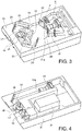
- the tips or front faces of the electrodes are illuminated using, in the example of Figures 3 and 5 , a pair of light sources 16, 17, preferably LED light sources, and a plurality of reflecting surfaces.
- the LED light sources 16 and 17 project light beams L1 and L2 which illuminate two optical diffusors 29 and 30 with a certain wavelength.
- the wavelength depends on the material combination between electrode and the welded metal sheets, to achieve optimal contrast of the contaminations on the electrode.
- the optical diffusor is preferably opal glass, due to its capability to shape the locally uneven beam profile intensity of the LED to a nearly perfect diffused (evenly distributed) beam profile intensity. This is necessary to achieve an equal illumination of the electrode front for measurements.
- the now diffuse light beams L1 and L2 are oriented in an intermediate geometrical plane p1 between the two seats or measurement places 14, 15.
- the light beams L1 and L2 are reflected from a set of front mirrors to the optical elements 24 and 25, as shown in Figures 5 and 6 .
- mirrors 18 and 19 are triangular front mirrors and 20 to 23 are flat front mirrors.
- the two light beams L1 and L2 converge on two respective obliquely reflecting optical elements 25 and 26. These elements are interposed between the two seats 14, 15 in which the electrodes E1, E2 are received ( Figure 6 ).
- the optical elements 25 and 26 are agglutinated rectangular prisms with reflective coated hypotenuses which extend in geometric planes which are skewed with respect to the intermediate geometrical plane p1. Due to this arrangement, the optical elements 25 and 26 reflect the light beams L1 and L2 perpendicularly to the geometric plane p1 in opposite directions, towards the front faces or tips of the electrodes E1, E2.
- the two oblique reflecting elements 25, 26 reflect the first and second light beams L1 and L2 in two opposite directions first and the second seat, where these beams hit the front faces or tips of the electrodes E1, E2.
- optical windows 27 and 28 which determine the positions and partly form the seats or measurement places and protect the optical system.
- the optical windows 27 and 28 are sapphire windows, sustained by the housing 10. These windows provide accurately located supporting points and abutments for the electrodes. Sapphire windows are preferred, since they are scratch resistant and mechanically strong enough to withstand the full closing force of a welding gun (approximately of 3.5 kN, 1.75 kN per window).
- These images are captured by an image recording means, in this embodiment a camera 31 with an objective 31a.
- the front images I1, I2 provide information on the wear and cleanness conditions of the electrode tips, as well as of their diameter.
- the front faces of the electrodes are illuminated using substantially the same optical path as that of the images of the electrodes returning to the camera 31 and camera objective 31a, as shown in Figures 3 , 5 and 7 .
- the light beams L1, L2 and the light sources 16, 17 are arranged symmetrically, on opposite sides of a symmetry plane p2 in which the camera 31 is located and oriented.
- the available space is further optimized by arranging the sets of reflecting surfaces 18-26 in such a way as to create two luminous paths according to a closed polygonal line (in this example according to a rectangle, Figures 5 and 7 ) thus reaching the two oblique reflecting elements 25, 26 which divert the two light beams on each of the front faces of the electrodes.
- optical components illustrated in Figure 3 can be mounted on an intermediate support frame 40 which embraces the intermediate geometric plane p1.
- the support frame 40 forms a plurality of seats and recesses for mounting said components in predetermined positions.
- FIG. 3 provides a single camera 31 adapted to capture images of the front faces of both of the two electrodes, according to other embodiments two separate cameras may be used, each intended to capture images of one of the electrode front faces.
- FIG. 12 An exemplary, alternative embodiment, providing two distinct cameras 31, 131, is schematically shown in a plan view in Figure 12 .
- two light sources 16, 17 project a respective pair of light beams L1 and L2 in a geometric plane intermediate between the electrode seats or measurement places 14, 15.
- the two oblique reflecting elements 25, 26 are placed in an intermediate position between the two light sources 16 and 17.
- the two beams L1, L2 emitted from these sources are aligned and directed toward one another, in a direction substantially perpendicular to the symmetry plane p2.
- a respective partially transparent reflecting element 18a, 19a Between each of the light sources 16, 17 and the oblique reflecting elements 25, 26 there is interposed a respective partially transparent reflecting element 18a, 19a.
- Figures 4 and 9 show one of two assemblies adapted to generate and capture side images of one of the electrodes, in this example lower electrode E2.
- a third light source 32 is used to emit a third light beam L3 to illuminate a side of the electrode E2 accommodated in the lower seat 15.
- a central part of the third light beam is obscured by the electrode E2, while a peripheral part I3 of this beam is captured by an image recording means 33, in this embodiment a camera with an objective 33a. That peripheral part of the third light beam that passes beyond the electrode E2 generates an image which is indicative of the size and shape of the contour of the electrode, and therefore of its condition of wear ( Figure 11 ).
- the third light beam L3 follows an angled or non-rectilinear path, being deflected by a reflecting surface 34.
- the third light beam L3 crosses an optical diffusor 35, in this embodiment opal glass, plus two sapphire windows 36 and 37. These are mounted on either side of the electrode E2, to protect the optical system.
- the components 32-37 shown in Figure 4 and 9 may be mounted on a lower support frame 41 preferably having a plurality of seats and recesses for fitting those components accurately in predetermined positions.
- the support frame 41 may be secured under the intermediate frame 40 within the housing 10.
- a second assembly identical to the one shown in Figures 4 and 9 , is designed to generate and capture side images of the upper electrode E1.
- the second assembly (visible in Figure 14 ) includes a fourth light source 43 emitting a fourth light beam L4 to illuminate a side of the electrode E1 located in the upper seat 14. A central part of the fourth light beam is obscured by the electrode E1, while a peripheral part I4 of this beam, which passes around and beyond the electrode E1, is captured as an image from an image recording means 44, such as a camera or video camera.
- the fourth light beam L4 may follow a non-rectilinear path deflected by a reflecting surface 45.
- a reflecting surface 45 Along the path of the fourth light beam L4 there may be fitted an opal glass 44 immediately downstream of the fourth light source 43 as well as two sapphire windows 47, 48 respectively located immediately upstream and downstream of the electrode E2.
- the components 43-48 may be mounted on a support frame bottom (not shown), similar to the upper frame 41 and having a plurality of seats and recesses for fitting components 43-48 accurately in predetermined positions.
- the lower support frame may be fixed on top of the intermediate support frame 40 within the housing 10.
- all the light beams may originate from a single light source rather than from individual, separate light sources.
- a single image recording means for example, a single camera or video camera, capable of recording images in frames or windows being part of a single overall image.
- the sensor device may also incorporate a pneumatic circuit (not shown) to keep those surfaces that come in contact with the electrode permanently clean.
- the sensor device may incorporate a CPU 24 ( figure 4 ) that is protected from contamination by external elements (dust, heat).
- the sensor device allows to simultaneously detect overall images of a pair of welding electrodes.
- the image of the side view ( Figure 11 ) provides information concerning the shape of the tip and the height that is left, for the decision to change or to dress the electrode.
- the side picture also gives information about the electrode wall thickness.
- the front view ( Figure 10 ) gives information about the grade of impurity and wear at the contact surface of the electrode caused by the welding process.
- the light sources may produce red, diffuse light ( ⁇ 650 nm) which gives the best contrast on copper electrodes used for steel sheet welding. Because of the usual purifications there is tin (from the steel sheet tin coating) which forms an intermetallic phase with the copper (bronze) and a carbon deposition (black dust) from the rests of oil on the steel sheets (coming from the cold drawing of the steel sheets). These purifications absorb the red wavelength mostly, while the copper reflects it, so one gets a good contrast between both. There may also be a blue illumination ( ⁇ 470 nm), integrated in the same light source (e.g. 2 blue and 2 red LEDs on the same board), individually controllable. Blue light is used for copper electrodes used to weld sheets of aluminum.
- red, diffuse light ⁇ 650 nm
- the aluminum forms also an intermetallic phase on the surface of the electrode.
- These purifications have also a high reflectivity, like copper in red wavelengths. So a blue light wavelength is used which reflects better on aluminum than on copper. This blue light is mostly absorbed on copper, but reflected by aluminum. As a result, the picture of aluminum purifications shows bright areas of dirt and dark areas of the copper.
- LEDs have proven to be the cheapest and most appropriate light sources, other discrete wavelength light sources may be used.
- a laser of a discrete wavelength may be used as a possible light source, although a laser is more costly and requires special arrangements for beam shaping to a relatively wide area to illuminate.
Landscapes
- Engineering & Computer Science (AREA)
- General Health & Medical Sciences (AREA)
- Immunology (AREA)
- Chemical & Material Sciences (AREA)
- Analytical Chemistry (AREA)
- Biochemistry (AREA)
- Physics & Mathematics (AREA)
- General Physics & Mathematics (AREA)
- Life Sciences & Earth Sciences (AREA)
- Pathology (AREA)
- Health & Medical Sciences (AREA)
- Mechanical Engineering (AREA)
- Quality & Reliability (AREA)
- Investigating Materials By The Use Of Optical Means Adapted For Particular Applications (AREA)
- Length Measuring Devices By Optical Means (AREA)
Description
- The present invention relates to an optical sensor device for detecting the conditions of spot welding electrodes.
- It is known that in spot welding plants, with use, the electrodes of the welding guns get worn, deformed and contaminated with metallic residues and oxide deposits. Therefore, the electrodes have to be frequently redressed to regain a clean and proper surface. As known, it is necessary to remove a certain thickness of contaminants that form on the electrode surfaces. The thickness of the contaminant deposit affects the overall electrical and thermal conductivity of the electrode. The shape and size of the electrode, in addition, have a determining influence on the size of the so-called "lens" of the weld. If the electrode tip is too wide, adequate fusion may not be achieved at the interface between the surfaces of the two metal sheets to be welded together.
- Typically, when the electrodes exceed a certain size, the operator compensates by increasing the intensity of the electrical current passing through the electrodes. The increased current leads to a number of unfavorable factors. First, the current increase causes an overheating of the cooling liquid and a subsequent enlargement of the welding electrode tips. Overheating causes a reduction of the electrode hardness and a deterioration of its mechanical characteristics. Along with this, a phenomenon known as "mushrooming" occurs, i.e. an increase in the diameter of the electrode and, with it, also the deposition of contaminants.
- A need is felt in this technical field to optimize the removal of material deposited on the electrodes. Heretofore, dressing processes have been carried out at regular intervals, according to standardized parameters, concerning the duration of the dressing phase and the clamping force with which the welding gun closes its electrodes on the dressing unit. Standard parameters, in terms of time and force, represent a compromise that is suitable in most cases. However, the removal of material occurs without a knowledge of the exact thickness of the surface layers of electrodes that should be removed.
- Further, dressing has heretofore been carried out in an undifferentiated manner to both the anode and the cathode. Since a greater deposit of contaminants occurs on the cathode, in order to optimize electrode duration and operation, deposits should be removed to a greater extent from the cathode than from the anode.
-
US2012/0200695 A1 deals with an electrode inspection apparatus for spot welding.DE 20 2006 004 456 U1 discloses a test device for surfaces, specially those of spot welding electrodes.EP 1 964 639 - Therefore it is a main object of the present invention to know the thickness of the surface layers to be removed, in order to perform the dressing in an optimized manner, that is, adjusting the dressing time (for example, 3 milliseconds) with a predetermined pressure (for example 150 daN), so as to remove only the oxide deposits and save the material of the electrodes which is still uncontaminated.
- Dressing optimization prolongs the useful life of the electrode. Consequently, this involves a reduction of the idle time required for stopping a production line in order to replace the worn electrodes. A standstill of a line involves an economic loss, which sometimes may even be unnecessary in case the electrodes do not really need to be redressed or replaced.
- A need is also felt to keep welding parameters constant and, particularly, the intensity of current which is applied and the closing and welding time the welding gun, so that these parameters are always correct and in compliance with optimized standards. Above all, one should avoid the risk that an inappropriate change in the intensity of current or in the duration of the current application causes defective welds. Another object of the invention, therefore, is to prevent or reduce the need for servicing in order to set the right welding parameters (current, time).
- A reduction in the number of manual operations is also beneficial, as it reduces the risk of accidents. Therefore, a further object of the invention is to increase safety for the personnel working on a welding line.
- A further object of the invention to reduce power consumption of the welding line, as well as a reduction in CO2 emissions.
- Another object of the invention is to certify the weld quality. Currently, the quality controls of modern welding systems are only able to certify that the welds were created in compliance with certain parameters (current intensity, time and force or pressure of closing of the welding gun). But a variation of electrode condition, caused by normal wear and contamination cannot be detected. Electrode condition is a major factor influencing weld quality and consequently frequent destructive tests of weld must be carried out. The invention is able to monitor and repair electrode shape and surface condition, enabling the motor vehicle manufacturers to certify all major process factors that can influence weld quality. This affords greater confidence in the reliability of the welding process and enables a reduction in the frequency of destructive tests.
- A further object of the invention is to provide a useful tool to certify that the welding points have been applied according to certain welding parameters (intensity of current applied, application time of the current, clamping force or pressure applied by the welding gun) and with electrodes having an optimal geometric shape. A quality certification may allow a reduction in the total number of welding spots applied to a given welded assembly, due to the welds being certified. Currently, the production of a motor vehicle requires 5000 to 6000 welding points. Since welding points are not certified, a rather high percentage of additional welding points are required for safety reasons.
- A still further object of the invention, therefore, is to reduce the number of welding points, as well as time and costs that this entails.
- Another object of the invention is to allow the selection of the most appropriate dressing tool, i.e. more or less aggressive, depending on the level of degradation of the electrodes.
- The above and other objects and advantages, which will be better understood hereinafter, are achieved according to the present invention by a sensor device having the features defined in
claim 1. Further preferred embodiments are defined in the appended claims. In summary, the sensor device is based on an optical reflection system, which illuminates the tip faces of the electrodes and takes measurements of both reflectivity and the area/shape of the tip surface. In this way, tip face diameter and material condition, which are the two key parameters determining the quality of the weld, will be assessed. The sensor device will generate, through a CPU, a quantitative measure of the quality electrode, preferably in the form of a percentage, on a scale between a fully clean and required tip face diameter, to a black or worn or excess diameter, which is a condition not capable of meeting weld quality requirements. This information will likely be relayed to and used by a control system for controlling a tip dress schedule. The same information may also be used to assess the rate of degradation or wear of the abrasive tooling. An appropriate kind of tool may be chosen as a function of the degradation status. A more or less aggressive kind of tooling (milling cutter) may be chosen accordingly. The sensor device may be conveniently located near a dresser unit. The sensor device will assess quality electrode tip dressing immediately after, or even before dressing. - The features and advantages of the invention will become apparent from the ensuing detailed description of a few preferred, but not limiting, embodiments thereof. Reference is made to the accompanying drawings, in which:
-
Figure 1 is a perspective view schematically illustrating a housing of an optical sensor device; -
Figure 2 is a perspective view of the housing ofFigure 1 , where some parts have been removed for illustrative purposes; -
Figure 3 is a perspective view of some inner parts of the sensor device, particularly a supporting plate with optical components for illuminating and obtaining images of the front faces of a pair of electrodes; -
Figure 4 is a perspective view schematically illustrating other inner parts of the sensor device, particularly a supporting plate with optical components for illuminating and obtaining a side view of one of the electrodes; -
Figure 5 is a plan view schematically illustrating the light paths of a pair of light beams which illuminate the front faces or tips of a pair of electrodes; -
Figure 6 is a schematic, vertical cross-sectional view taken along line VI-VI ofFigure 5 , showing vertical parts of the light paths for illuminating the front faces of the electrodes; -
Figure 7 is a schematic view illustrating optical paths of images of the front faces of the electrodes; -
Figure 8 is a schematic cross-sectional view taken along on the line VIII-VIII ofFigure 7 , showing the vertical part of optical paths followed by images of the front faces of the electrodes; -
Figure 9 is a schematic plan view of the path of a light beam that illuminates a side surface of one of the electrodes; -
Figure 10 are pictures, as taken by a camera, of the front faces or tips of the electrodes; -
Figure 11 is a picture, as taken by a camera, showing a side view of an electrode; -
Figure 12 is a schematic plan view of an optical system capable of obtaining images of the front faces of a pair of electrodes, according to an alternative embodiment of the invention; -
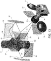
Figure 13 is a perspective view illustrating the working principle for taking images of the front faces or tips of the electrodes; -
Figure 14 is a perspective view illustrating the working principle for taking images of the sides of the electrodes; and -
Figure 15 is a perspective view illustrating the working principle for taking images of the front faces and the sides the electrodes. - Referring initially to
Figures 1 and 2 , numeral 10 designates in its entirety a housing of an optical sensor device according to an embodiment of the invention. The optical sensor device is designed to detect images of a pair of spot welding electrodes carried by a welding gun. Welding guns are generally known, and therefore will not be described nor illustrated. - The
housing 10 has a pair ofopenings openings 11. Only one of theopenings 11 is visible inFigures 1 and 2 ; asimilar opening 11a is formed in the side of the housing opposite toside 12. - In order to prevent the entrance of light, dust and other impurities within the
housing 10, theopenings brush stripes 13. InFigure 2 thebrush stripes 13 have been removed only for illustrative purposes. - A pair of seats or measurement places 14, 15, separated from each other, are provided inside the
openings seat - The tips or front faces of the electrodes are illuminated using, in the example of
Figures 3 and5 , a pair oflight sources - The
LED light sources optical diffusors - The now diffuse light beams L1 and L2 are oriented in an intermediate geometrical plane p1 between the two seats or measurement places 14, 15. The light beams L1 and L2 are reflected from a set of front mirrors to the
optical elements Figures 5 and 6 . In this example, mirrors 18 and 19 are triangular front mirrors and 20 to 23 are flat front mirrors. - The two light beams L1 and L2 converge on two respective obliquely reflecting
optical elements seats Figure 6 ). According to a preferred embodiment, theoptical elements optical elements - The two
oblique reflecting elements - The electrodes E1 and E2 are docked onto
optical windows optical windows housing 10. These windows provide accurately located supporting points and abutments for the electrodes. Sapphire windows are preferred, since they are scratch resistant and mechanically strong enough to withstand the full closing force of a welding gun (approximately of 3.5 kN, 1.75 kN per window). - The light beams L1 and L2, incident on the front faces of the electrodes, produce respective images I1, I2 that follow a reverse path between the mirrors, as depicted schematically in
Figure 7 . These images are captured by an image recording means, in this embodiment acamera 31 with an objective 31a. As schematically shown inFigure 10 , the front images I1, I2 provide information on the wear and cleanness conditions of the electrode tips, as well as of their diameter. The front faces of the electrodes are illuminated using substantially the same optical path as that of the images of the electrodes returning to thecamera 31 and camera objective 31a, as shown inFigures 3 ,5 and 7 . - According to a particularly compact embodiment, the light beams L1, L2 and the
light sources camera 31 is located and oriented. The available space is further optimized by arranging the sets of reflecting surfaces 18-26 in such a way as to create two luminous paths according to a closed polygonal line (in this example according to a rectangle,Figures 5 and 7 ) thus reaching the twooblique reflecting elements - The optical components illustrated in
Figure 3 (light sources intermediate support frame 40 which embraces the intermediate geometric plane p1. According to an advantageous embodiment, thesupport frame 40 forms a plurality of seats and recesses for mounting said components in predetermined positions. - Although the embodiment illustrated in
Figure 3 provides asingle camera 31 adapted to capture images of the front faces of both of the two electrodes, according to other embodiments two separate cameras may be used, each intended to capture images of one of the electrode front faces. - An exemplary, alternative embodiment, providing two
distinct cameras Figure 12 . According toFigure 12 , for illuminating the front faces of the electrodes, twolight sources oblique reflecting elements light sources light sources oblique reflecting elements element source oblique reflecting element oblique reflecting element respective camera -
Figures 4 and9 show one of two assemblies adapted to generate and capture side images of one of the electrodes, in this example lower electrode E2. - A third
light source 32 is used to emit a third light beam L3 to illuminate a side of the electrode E2 accommodated in thelower seat 15. A central part of the third light beam is obscured by the electrode E2, while a peripheral part I3 of this beam is captured by an image recording means 33, in this embodiment a camera with an objective 33a. That peripheral part of the third light beam that passes beyond the electrode E2 generates an image which is indicative of the size and shape of the contour of the electrode, and therefore of its condition of wear (Figure 11 ). - In the embodiment shown in
Figures 4 and9 , in order to optimize the available space within the housing, the third light beam L3 follows an angled or non-rectilinear path, being deflected by a reflectingsurface 34. The third light beam L3 crosses anoptical diffusor 35, in this embodiment opal glass, plus twosapphire windows - The components 32-37 shown in
Figure 4 and9 may be mounted on alower support frame 41 preferably having a plurality of seats and recesses for fitting those components accurately in predetermined positions. Thesupport frame 41 may be secured under theintermediate frame 40 within thehousing 10. - According to a preferred embodiment, a second assembly, identical to the one shown in
Figures 4 and9 , is designed to generate and capture side images of the upper electrode E1. The second assembly (visible inFigure 14 ) includes a fourthlight source 43 emitting a fourth light beam L4 to illuminate a side of the electrode E1 located in theupper seat 14. A central part of the fourth light beam is obscured by the electrode E1, while a peripheral part I4 of this beam, which passes around and beyond the electrode E1, is captured as an image from an image recording means 44, such as a camera or video camera. - Similarly to the assembly shown in
Figure 4 , and according to a substantially identical planimetric arrangement, the fourth light beam L4 may follow a non-rectilinear path deflected by a reflectingsurface 45. Along the path of the fourth light beam L4 there may be fitted anopal glass 44 immediately downstream of the fourthlight source 43 as well as twosapphire windows - According to an embodiment, the components 43-48 may be mounted on a support frame bottom (not shown), similar to the
upper frame 41 and having a plurality of seats and recesses for fitting components 43-48 accurately in predetermined positions. The lower support frame may be fixed on top of theintermediate support frame 40 within thehousing 10. - In accordance with a further embodiment, all the light beams, namely both those intended to provide images of the front faces, and both those intended to provide information and images of the contour of the electrodes, may originate from a single light source rather than from individual, separate light sources.
- Likewise, by suitably rearranging the reflecting surfaces, it is possible to direct all images to a single image recording means, for example, a single camera or video camera, capable of recording images in frames or windows being part of a single overall image.
- The sensor device may also incorporate a pneumatic circuit (not shown) to keep those surfaces that come in contact with the electrode permanently clean.
- The sensor device may incorporate a CPU 24 (
figure 4 ) that is protected from contamination by external elements (dust, heat). - As will be appreciated, the sensor device allows to simultaneously detect overall images of a pair of welding electrodes.
- The image of the side view (
Figure 11 ) provides information concerning the shape of the tip and the height that is left, for the decision to change or to dress the electrode. The side picture also gives information about the electrode wall thickness. The front view (Figure 10 ) gives information about the grade of impurity and wear at the contact surface of the electrode caused by the welding process. - According to an embodiment, the light sources may produce red, diffuse light (∼ 650 nm) which gives the best contrast on copper electrodes used for steel sheet welding. Because of the usual purifications there is tin (from the steel sheet tin coating) which forms an intermetallic phase with the copper (bronze) and a carbon deposition (black dust) from the rests of oil on the steel sheets (coming from the cold drawing of the steel sheets). These purifications absorb the red wavelength mostly, while the copper reflects it, so one gets a good contrast between both. There may also be a blue illumination (∼470 nm), integrated in the same light source (e.g. 2 blue and 2 red LEDs on the same board), individually controllable. Blue light is used for copper electrodes used to weld sheets of aluminum. In this case the aluminum forms also an intermetallic phase on the surface of the electrode. These purifications have also a high reflectivity, like copper in red wavelengths. So a blue light wavelength is used which reflects better on aluminum than on copper. This blue light is mostly absorbed on copper, but reflected by aluminum. As a result, the picture of aluminum purifications shows bright areas of dirt and dark areas of the copper.
- Although LEDs have proven to be the cheapest and most appropriate light sources, other discrete wavelength light sources may be used. For example, a laser of a discrete wavelength may be used as a possible light source, although a laser is more costly and requires special arrangements for beam shaping to a relatively wide area to illuminate.
- A number of embodiments and aspects of the invention have been disclosed. It is to be understood that each embodiment may be combined with any other aspect/embodiment. Moreover, the invention is not restricted to the described embodiments, but may be varied within the scope of the accompanying claims and their legal equivalents.
Claims (12)
- An optical sensor device for detecting images of a pair of spot welding electrodes (E1, E2) carried by a welding gun, the device comprising:- a housing (10) having at least one pair of openings (11, 11a) ;- at least a first (14) and a second (15) seat spaced from one another within the housing, each seat communicating with a respective one of the openings (11, 11a), each seat (14, 15) being adapted to accommodate one of the electrodes carried by the welding gun;- first illuminating means (16, 17) adapted to emit a first (L1) and a second (L2) light beam in an intermediate geometric plane (p1) between the seats (14, 15);- two oblique reflecting elements (25, 26), interposed between the two seats (14, 15), the oblique reflecting elements being adapted to reflect the first (L1) and second (L2) light beams in two opposite directions perpendicular to the geometric plane (p1) toward the first and the second seat;- second illuminating means (43, 32) adapted to emit third (L3) and fourth (L4) light beams on opposite sides of said geometric plane (p1) to illuminate the first and the second seat (14, 15);- image recording means (31, 131, 33, 44) adapted to capture images (I1, I2) reflected by the two oblique reflecting elements (25, 26) and at least part of the third and fourth light beams (L3, L4) downstream of the first and second seats (14, 15) along paths of the third and fourth light beams.
- An optical sensor device according to claim 1, wherein the illuminating means comprise discrete wavelength light sources.
- An optical sensor device according to claim 1 or 2, wherein the illuminating means comprise LEDs as light sources.
- An optical sensor device according to claim 1 or 2 or 3, wherein the illuminating means comprise light sources emitting red, diffuse light with a wavelength of about 650 nm.
- An optical sensor device according to any one of the preceding claims, wherein the image recording means include cameras with objectives.
- An optical sensor device according to any one of the preceding claims, wherein the obliquely reflecting optical elements (25, 26) comprise agglutinated rectangular prisms with reflective coated hypotenuses extending in geometric planes which are skewed with respect to the intermediate geometrical plane (p1).
- An optical sensor device according to any one of the preceding claims, wherein each seat (14, 15) is provided with a fixed optical window (27, 28) providing an abutment surface for each electrode (E1, E2).
- An optical sensor device according to claim 7, wherein the optical windows (27, 28) comprise sapphire windows.
- An optical sensor device according to any one of the preceding claims, wherein each opening (11, 11a) is provided with brush means (13) for preventing light and dust from entering the housing (10).
- An optical sensor device according to any one of the preceding claims, wherein
the first illuminating means comprise two light sources (16, 17) arranged on opposite sides of a symmetry plane (p2) for projecting the first and second light beams (L1, L2) onto two sets of mirrors (18, 20, 21; and 19, 22, 23) so arranges as to reflect the first and second light beams on the two oblique reflecting elements (25, 26), and
the image recording means comprise a single image recording means (31) oriented in the symmetry plane towards the two sets of mirrors so as to capture images (I1, I2) reflected back by the two oblique reflecting elements (25, 26) and the two sets of mirrors. - An optical sensor device according to any one of claims 1 to 9, wherein the two sets of mirrors (18, 20, 21; and 19, 22, 23) are so arranged as to determine two luminous paths according to a closed polygonal line, whereby the first and second light beams (L1, 12) projected from the two light sources (16, 17) reach the two oblique reflecting elements (25, 26) which divert the two light beams (L1, L2) on each of the front faces of the electrodes (E1, E2).
- An optical sensor device according to any of the preceding claims, wherein
the first illuminating means comprise two light sources (16, 17), and the two oblique reflecting elements (25, 26) are arranged in an intermediate position between the two light sources (16, 17), whereby the two light beams (L1, L2) emitted from the light sources (16, 17) are aligned and directed toward one another, and wherein
between each of the light sources (16, 17) and the oblique reflecting elements (25, 26) there is interposed a respective partially transparent reflecting element (18a, 19a) which leaves the respective light beam (L1, L2) coming directly from the light source (16, 17) filter towards the respective oblique reflecting element (25, 26) and reflects a front image (I1, I2) of the respective electrode (E1, E2), coming from the same oblique reflecting element (25, 26), towards a respective one of two image recording means (31, 131).
Priority Applications (1)
| Application Number | Priority Date | Filing Date | Title |
|---|---|---|---|
| SI201330600T SI2938454T1 (en) | 2013-08-01 | 2013-08-01 | An optical device for detecting quality of welding gun electrodes |
Applications Claiming Priority (1)
| Application Number | Priority Date | Filing Date | Title |
|---|---|---|---|
| PCT/EP2013/066201 WO2015014404A1 (en) | 2013-08-01 | 2013-08-01 | An optical device for detecting quality of welding gun electrodes |
Publications (2)
| Publication Number | Publication Date |
|---|---|
| EP2938454A1 EP2938454A1 (en) | 2015-11-04 |
| EP2938454B1 true EP2938454B1 (en) | 2017-02-22 |
Family
ID=48948403
Family Applications (1)
| Application Number | Title | Priority Date | Filing Date |
|---|---|---|---|
| EP13745824.6A Active EP2938454B1 (en) | 2013-08-01 | 2013-08-01 | An optical device for detecting quality of welding gun electrodes |
Country Status (14)
| Country | Link |
|---|---|
| US (1) | US9417192B2 (en) |
| EP (1) | EP2938454B1 (en) |
| JP (1) | JP6266776B2 (en) |
| KR (1) | KR102059711B1 (en) |
| CN (1) | CN105026094B (en) |
| BR (1) | BR112015019805B1 (en) |
| CA (1) | CA2899534C (en) |
| ES (1) | ES2622891T3 (en) |
| HU (1) | HUE032750T2 (en) |
| MX (1) | MX362326B (en) |
| PL (1) | PL2938454T3 (en) |
| PT (1) | PT2938454T (en) |
| SI (1) | SI2938454T1 (en) |
| WO (1) | WO2015014404A1 (en) |
Families Citing this family (11)
| Publication number | Priority date | Publication date | Assignee | Title |
|---|---|---|---|---|
| KR101754732B1 (en) * | 2015-10-29 | 2017-07-19 | 주식회사휴비스 | Inspection apparatus capable of real-time monitoring for electrode tip of welder and welding system with inspection apparatus |
| CN107764315A (en) * | 2016-08-22 | 2018-03-06 | 北京汽车股份有限公司 | Spot-wedling electrode detection means and its detection method |
| KR101926635B1 (en) * | 2016-12-05 | 2018-12-07 | 오토아이티(주) | Inspection apparatus for welding tip of spot welding gun |
| KR101900330B1 (en) * | 2016-12-05 | 2018-11-08 | 오토아이티(주) | Inspection apparatus for welding tip of spot welding gun |
| KR102000441B1 (en) * | 2018-06-04 | 2019-07-16 | 아진산업(주) | Welding tip inspection apparatus having multiple windows mirror |
| JP7363550B2 (en) * | 2020-02-10 | 2023-10-18 | マツダ株式会社 | Method and device for determining dress quality of resistance welding electrodes |
| CN111579559B (en) * | 2020-04-24 | 2023-05-12 | 北京现代汽车有限公司 | Detection tool of electrode tip detection machine |
| KR102875270B1 (en) | 2020-10-22 | 2025-10-23 | 주식회사 엘지에너지솔루션 | Apparatus For Testing Device of Welding Rod And Testing Method Using It |
| CN113414482B (en) * | 2021-06-15 | 2023-05-16 | 中国第一汽车股份有限公司 | Device and method for detecting position compensation function of spot welding electrode of robot |
| KR102946285B1 (en) | 2023-03-23 | 2026-04-01 | 오토아이티(주) | System for integrated inspection of welding tip condition |
| CN116642896A (en) * | 2023-05-15 | 2023-08-25 | 广东奥普特科技股份有限公司 | A combined detection device and detection system |
Family Cites Families (22)
| Publication number | Priority date | Publication date | Assignee | Title |
|---|---|---|---|---|
| US4491719A (en) * | 1982-12-20 | 1985-01-01 | General Electric Company | Light pattern projector especially for welding |
| US4711986A (en) * | 1986-11-24 | 1987-12-08 | General Electric Company | Method and apparatus for measuring weld penetration in an arc welding process |
| JPH0466279A (en) * | 1990-07-04 | 1992-03-02 | Toshiaki Shimada | Spot welding method |
| JPH0465608A (en) * | 1990-07-04 | 1992-03-02 | Toshiaki Shimada | Measuring method for tip shape of electrode rod for spot-welding |
| US5332342A (en) * | 1991-04-26 | 1994-07-26 | Honda Giken Kogyo Kabushiki Kaisha | Electrode tip dresser and cutter for electrode tip dresser |
| JP2002122418A (en) * | 2000-10-18 | 2002-04-26 | Maki Mfg Co Ltd | Measuring device |
| US6744012B2 (en) * | 2000-12-07 | 2004-06-01 | Honda Giken Kogyo Kabushiki Kaisha | Control method of arc welding and arc welder |
| JP3838561B2 (en) * | 2002-06-19 | 2006-10-25 | 東レエンジニアリング株式会社 | Mounting apparatus and mounting method |
| CN100522453C (en) * | 2003-12-10 | 2009-08-05 | 菲茨有限责任公司 | Track welding device for pipeline erection |
| DE102004008038B4 (en) * | 2004-02-19 | 2014-05-22 | Lutz Precision, K.S. | Elektrodenzustandsmeßeinrichtung |
| DE102007013038B4 (en) | 2006-03-21 | 2017-06-22 | Pepperl + Fuchs Gmbh | Double test device for a pair of welding electrodes |
| DE202006004456U1 (en) * | 2006-03-21 | 2007-08-02 | Pepperl + Fuchs Gmbh | Test device for surfaces, in particular of welding electrodes |
| EP1964639A1 (en) * | 2007-02-28 | 2008-09-03 | Abb Research Ltd. | Method of and system for controlling tools comprising spot welding electrodes using image obtaining and comparison means |
| US8847100B2 (en) * | 2008-01-08 | 2014-09-30 | Fanuc America Corporation | Weld cap and tip inspection method and apparatus |
| JP2010120035A (en) * | 2008-11-18 | 2010-06-03 | Kyokutoh Co Ltd | Apparatus of determining normal/defective condition of electrode chip |
| DE112010004153B4 (en) * | 2009-10-27 | 2017-04-27 | Keylex Corp. | DEVICE FOR INSPECTION OF ELECTRODES FOR POINT WELDING |
| JP5048097B2 (en) * | 2010-04-05 | 2012-10-17 | ファナック株式会社 | Spot welding system and dressing determination method |
| EP2429272A2 (en) * | 2010-09-10 | 2012-03-14 | Chatsworth Products, Inc. | Cable pass-through panel for electronic equipment enclosure |
| JP2012072725A (en) * | 2010-09-29 | 2012-04-12 | Kyocera Corp | Structure for internal combustion engine, internal combustion engine with position detection mechanism and internal combustion engine with liquid state detection mechanism |
| JP5216882B2 (en) * | 2011-02-22 | 2013-06-19 | 株式会社キョクトー | Electrode tip pass / fail judgment device |
| JP5695456B2 (en) * | 2011-03-08 | 2015-04-08 | 株式会社キーレックス | Electrode inspection device for spot welding |
| KR101490938B1 (en) | 2013-12-20 | 2015-02-06 | 기아자동차 주식회사 | Welding facility inspecting system |
-
2013
- 2013-08-01 EP EP13745824.6A patent/EP2938454B1/en active Active
- 2013-08-01 ES ES13745824.6T patent/ES2622891T3/en active Active
- 2013-08-01 WO PCT/EP2013/066201 patent/WO2015014404A1/en not_active Ceased
- 2013-08-01 MX MX2015010676A patent/MX362326B/en active IP Right Grant
- 2013-08-01 HU HUE13745824A patent/HUE032750T2/en unknown
- 2013-08-01 CA CA2899534A patent/CA2899534C/en active Active
- 2013-08-01 JP JP2016530358A patent/JP6266776B2/en active Active
- 2013-08-01 PT PT137458246T patent/PT2938454T/en unknown
- 2013-08-01 KR KR1020157023528A patent/KR102059711B1/en active Active
- 2013-08-01 BR BR112015019805A patent/BR112015019805B1/en not_active IP Right Cessation
- 2013-08-01 SI SI201330600T patent/SI2938454T1/en unknown
- 2013-08-01 US US14/771,078 patent/US9417192B2/en active Active
- 2013-08-01 PL PL13745824T patent/PL2938454T3/en unknown
- 2013-08-01 CN CN201380074366.7A patent/CN105026094B/en active Active
Non-Patent Citations (1)
| Title |
|---|
| None * |
Also Published As
| Publication number | Publication date |
|---|---|
| BR112015019805A2 (en) | 2017-07-18 |
| CA2899534A1 (en) | 2015-02-05 |
| US20160131597A1 (en) | 2016-05-12 |
| KR20160034845A (en) | 2016-03-30 |
| WO2015014404A1 (en) | 2015-02-05 |
| US9417192B2 (en) | 2016-08-16 |
| CA2899534C (en) | 2020-03-24 |
| PL2938454T3 (en) | 2017-08-31 |
| MX2015010676A (en) | 2015-12-16 |
| JP6266776B2 (en) | 2018-01-24 |
| MX362326B (en) | 2019-01-11 |
| EP2938454A1 (en) | 2015-11-04 |
| ES2622891T3 (en) | 2017-07-07 |
| JP2016525690A (en) | 2016-08-25 |
| HUE032750T2 (en) | 2017-10-30 |
| SI2938454T1 (en) | 2017-08-31 |
| BR112015019805B1 (en) | 2020-04-07 |
| CN105026094A (en) | 2015-11-04 |
| PT2938454T (en) | 2017-04-20 |
| CN105026094B (en) | 2017-04-26 |
| KR102059711B1 (en) | 2019-12-26 |
Similar Documents
| Publication | Publication Date | Title |
|---|---|---|
| CA2899534C (en) | An optical device for detecting quality of welding gun electrodes | |
| US8953033B2 (en) | Electrode inspection apparatus for spot welding | |
| KR101102627B1 (en) | Systems and methods for identifying debris, debris and defects during the manufacture of composite structures | |
| CA2663314C (en) | Method and device for the optical assessment of welding quality during welding | |
| KR101140072B1 (en) | Device and method for detecting defect at glass sheet end surface | |
| EP1600247B1 (en) | Nozzle checker for laser beam machine | |
| CN101454112B (en) | Device for evaluating images of weld spots on a carrier material | |
| US9125246B2 (en) | Heatable glazing inspection | |
| CN109211939B (en) | Defect detection device, module and detection method for laser welding protective lens | |
| KR101360301B1 (en) | Changing time determining apparatus for electrode tip of a spot welding machine | |
| CN113514476B (en) | Automatic monitoring device for pollution of vibrating mirror protection lens | |
| JP2009512839A (en) | Glass plate optical inspection system and method | |
| JP2025517043A (en) | Analytical equipment for condition monitoring of protective glass in manufacturing equipment and manufacturing equipment for additive manufacturing processes | |
| CN114858817A (en) | Detection device and method for protective lens of galvanometer | |
| CN209327241U (en) | Laser Welding protects the defect detecting device of eyeglass, module | |
| JP2017087221A (en) | Real time monitoring permitting electrode chip inspection device and welding system provided with the same | |
| WO1999006676A1 (en) | Valve seat insert gaging system | |
| KR20170000122U (en) | Tip checker | |
| US20260105594A1 (en) | Method for detecting wear on ultrasonic tools | |
| CN222913521U (en) | Electrode cap of welding tongs and detection device of connecting piece of electrode cap | |
| JP2001334381A (en) | Output head of laser processing machine | |
| JPH01113175A (en) | Method for detecting welding abnormality | |
| KR20070091870A (en) | Lighting equipment used for flat panel display panel inspection |
Legal Events
| Date | Code | Title | Description |
|---|---|---|---|
| PUAI | Public reference made under article 153(3) epc to a published international application that has entered the european phase |
Free format text: ORIGINAL CODE: 0009012 |
|
| 17P | Request for examination filed |
Effective date: 20150728 |
|
| AK | Designated contracting states |
Kind code of ref document: A1 Designated state(s): AL AT BE BG CH CY CZ DE DK EE ES FI FR GB GR HR HU IE IS IT LI LT LU LV MC MK MT NL NO PL PT RO RS SE SI SK SM TR |
|
| AX | Request for extension of the european patent |
Extension state: BA ME |
|
| REG | Reference to a national code |
Ref country code: DE Ref legal event code: R079 Ref document number: 602013017689 Country of ref document: DE Free format text: PREVIOUS MAIN CLASS: B23K0011300000 Ipc: G01N0021880000 |
|
| GRAP | Despatch of communication of intention to grant a patent |
Free format text: ORIGINAL CODE: EPIDOSNIGR1 |
|
| RIC1 | Information provided on ipc code assigned before grant |
Ipc: B23K 31/12 20060101ALI20160714BHEP Ipc: G01N 21/88 20060101AFI20160714BHEP Ipc: B23K 11/30 20060101ALI20160714BHEP Ipc: G01N 21/94 20060101ALI20160714BHEP |
|
| DAX | Request for extension of the european patent (deleted) | ||
| INTG | Intention to grant announced |
Effective date: 20160728 |
|
| GRAS | Grant fee paid |
Free format text: ORIGINAL CODE: EPIDOSNIGR3 |
|
| GRAJ | Information related to disapproval of communication of intention to grant by the applicant or resumption of examination proceedings by the epo deleted |
Free format text: ORIGINAL CODE: EPIDOSDIGR1 |
|
| GRAL | Information related to payment of fee for publishing/printing deleted |
Free format text: ORIGINAL CODE: EPIDOSDIGR3 |
|
| INTC | Intention to grant announced (deleted) | ||
| RIN1 | Information on inventor provided before grant (corrected) |
Inventor name: LEUCKEFELD, MICHAEL Inventor name: PUEGNER, TINO Inventor name: KNOBBE, JENS |
|
| GRAR | Information related to intention to grant a patent recorded |
Free format text: ORIGINAL CODE: EPIDOSNIGR71 |
|
| GRAA | (expected) grant |
Free format text: ORIGINAL CODE: 0009210 |
|
| AK | Designated contracting states |
Kind code of ref document: B1 Designated state(s): AL AT BE BG CH CY CZ DE DK EE ES FI FR GB GR HR HU IE IS IT LI LT LU LV MC MK MT NL NO PL PT RO RS SE SI SK SM TR |
|
| INTG | Intention to grant announced |
Effective date: 20170113 |
|
| REG | Reference to a national code |
Ref country code: GB Ref legal event code: FG4D |
|
| REG | Reference to a national code |
Ref country code: CH Ref legal event code: EP |
|
| REG | Reference to a national code |
Ref country code: AT Ref legal event code: REF Ref document number: 869636 Country of ref document: AT Kind code of ref document: T Effective date: 20170315 |
|
| REG | Reference to a national code |
Ref country code: IE Ref legal event code: FG4D |
|
| REG | Reference to a national code |
Ref country code: DE Ref legal event code: R096 Ref document number: 602013017689 Country of ref document: DE |
|
| REG | Reference to a national code |
Ref country code: PT Ref legal event code: SC4A Ref document number: 2938454 Country of ref document: PT Date of ref document: 20170420 Kind code of ref document: T Free format text: AVAILABILITY OF NATIONAL TRANSLATION Effective date: 20170410 |
|
| REG | Reference to a national code |
Ref country code: SE Ref legal event code: TRGR |
|
| REG | Reference to a national code |
Ref country code: LT Ref legal event code: MG4D |
|
| REG | Reference to a national code |
Ref country code: NL Ref legal event code: MP Effective date: 20170222 |
|
| REG | Reference to a national code |
Ref country code: ES Ref legal event code: FG2A Ref document number: 2622891 Country of ref document: ES Kind code of ref document: T3 Effective date: 20170707 |
|
| REG | Reference to a national code |
Ref country code: AT Ref legal event code: MK05 Ref document number: 869636 Country of ref document: AT Kind code of ref document: T Effective date: 20170222 |
|
| PG25 | Lapsed in a contracting state [announced via postgrant information from national office to epo] |
Ref country code: GR Free format text: LAPSE BECAUSE OF FAILURE TO SUBMIT A TRANSLATION OF THE DESCRIPTION OR TO PAY THE FEE WITHIN THE PRESCRIBED TIME-LIMIT Effective date: 20170523 Ref country code: HR Free format text: LAPSE BECAUSE OF FAILURE TO SUBMIT A TRANSLATION OF THE DESCRIPTION OR TO PAY THE FEE WITHIN THE PRESCRIBED TIME-LIMIT Effective date: 20170222 Ref country code: NO Free format text: LAPSE BECAUSE OF FAILURE TO SUBMIT A TRANSLATION OF THE DESCRIPTION OR TO PAY THE FEE WITHIN THE PRESCRIBED TIME-LIMIT Effective date: 20170522 Ref country code: LT Free format text: LAPSE BECAUSE OF FAILURE TO SUBMIT A TRANSLATION OF THE DESCRIPTION OR TO PAY THE FEE WITHIN THE PRESCRIBED TIME-LIMIT Effective date: 20170222 Ref country code: FI Free format text: LAPSE BECAUSE OF FAILURE TO SUBMIT A TRANSLATION OF THE DESCRIPTION OR TO PAY THE FEE WITHIN THE PRESCRIBED TIME-LIMIT Effective date: 20170222 |
|
| PG25 | Lapsed in a contracting state [announced via postgrant information from national office to epo] |
Ref country code: NL Free format text: LAPSE BECAUSE OF NON-PAYMENT OF DUE FEES Effective date: 20170222 Ref country code: RS Free format text: LAPSE BECAUSE OF FAILURE TO SUBMIT A TRANSLATION OF THE DESCRIPTION OR TO PAY THE FEE WITHIN THE PRESCRIBED TIME-LIMIT Effective date: 20170222 Ref country code: AT Free format text: LAPSE BECAUSE OF FAILURE TO SUBMIT A TRANSLATION OF THE DESCRIPTION OR TO PAY THE FEE WITHIN THE PRESCRIBED TIME-LIMIT Effective date: 20170222 Ref country code: LV Free format text: LAPSE BECAUSE OF FAILURE TO SUBMIT A TRANSLATION OF THE DESCRIPTION OR TO PAY THE FEE WITHIN THE PRESCRIBED TIME-LIMIT Effective date: 20170222 |
|
| REG | Reference to a national code |
Ref country code: FR Ref legal event code: PLFP Year of fee payment: 5 |
|
| REG | Reference to a national code |
Ref country code: SK Ref legal event code: T3 Ref document number: E 24012 Country of ref document: SK |
|
| REG | Reference to a national code |
Ref country code: HU Ref legal event code: AG4A Ref document number: E032750 Country of ref document: HU |
|
| PG25 | Lapsed in a contracting state [announced via postgrant information from national office to epo] |
Ref country code: RO Free format text: LAPSE BECAUSE OF FAILURE TO SUBMIT A TRANSLATION OF THE DESCRIPTION OR TO PAY THE FEE WITHIN THE PRESCRIBED TIME-LIMIT Effective date: 20170222 Ref country code: EE Free format text: LAPSE BECAUSE OF FAILURE TO SUBMIT A TRANSLATION OF THE DESCRIPTION OR TO PAY THE FEE WITHIN THE PRESCRIBED TIME-LIMIT Effective date: 20170222 |
|
| REG | Reference to a national code |
Ref country code: DE Ref legal event code: R097 Ref document number: 602013017689 Country of ref document: DE |
|
| PG25 | Lapsed in a contracting state [announced via postgrant information from national office to epo] |
Ref country code: SM Free format text: LAPSE BECAUSE OF FAILURE TO SUBMIT A TRANSLATION OF THE DESCRIPTION OR TO PAY THE FEE WITHIN THE PRESCRIBED TIME-LIMIT Effective date: 20170222 Ref country code: DK Free format text: LAPSE BECAUSE OF FAILURE TO SUBMIT A TRANSLATION OF THE DESCRIPTION OR TO PAY THE FEE WITHIN THE PRESCRIBED TIME-LIMIT Effective date: 20170222 |
|
| PLBE | No opposition filed within time limit |
Free format text: ORIGINAL CODE: 0009261 |
|
| STAA | Information on the status of an ep patent application or granted ep patent |
Free format text: STATUS: NO OPPOSITION FILED WITHIN TIME LIMIT |
|
| 26N | No opposition filed |
Effective date: 20171123 |
|
| REG | Reference to a national code |
Ref country code: CH Ref legal event code: PL |
|
| PG25 | Lapsed in a contracting state [announced via postgrant information from national office to epo] |
Ref country code: MC Free format text: LAPSE BECAUSE OF FAILURE TO SUBMIT A TRANSLATION OF THE DESCRIPTION OR TO PAY THE FEE WITHIN THE PRESCRIBED TIME-LIMIT Effective date: 20170222 |
|
| PG25 | Lapsed in a contracting state [announced via postgrant information from national office to epo] |
Ref country code: LI Free format text: LAPSE BECAUSE OF NON-PAYMENT OF DUE FEES Effective date: 20170831 Ref country code: CH Free format text: LAPSE BECAUSE OF NON-PAYMENT OF DUE FEES Effective date: 20170831 |
|
| REG | Reference to a national code |
Ref country code: IE Ref legal event code: MM4A |
|
| PG25 | Lapsed in a contracting state [announced via postgrant information from national office to epo] |
Ref country code: LU Free format text: LAPSE BECAUSE OF NON-PAYMENT OF DUE FEES Effective date: 20170801 |
|
| PG25 | Lapsed in a contracting state [announced via postgrant information from national office to epo] |
Ref country code: IE Free format text: LAPSE BECAUSE OF NON-PAYMENT OF DUE FEES Effective date: 20170801 |
|
| REG | Reference to a national code |
Ref country code: FR Ref legal event code: PLFP Year of fee payment: 6 |
|
| PG25 | Lapsed in a contracting state [announced via postgrant information from national office to epo] |
Ref country code: MT Free format text: LAPSE BECAUSE OF NON-PAYMENT OF DUE FEES Effective date: 20170801 |
|
| PG25 | Lapsed in a contracting state [announced via postgrant information from national office to epo] |
Ref country code: CY Free format text: LAPSE BECAUSE OF FAILURE TO SUBMIT A TRANSLATION OF THE DESCRIPTION OR TO PAY THE FEE WITHIN THE PRESCRIBED TIME-LIMIT Effective date: 20170222 |
|
| PG25 | Lapsed in a contracting state [announced via postgrant information from national office to epo] |
Ref country code: MK Free format text: LAPSE BECAUSE OF FAILURE TO SUBMIT A TRANSLATION OF THE DESCRIPTION OR TO PAY THE FEE WITHIN THE PRESCRIBED TIME-LIMIT Effective date: 20170222 |
|
| PG25 | Lapsed in a contracting state [announced via postgrant information from national office to epo] |
Ref country code: AL Free format text: LAPSE BECAUSE OF FAILURE TO SUBMIT A TRANSLATION OF THE DESCRIPTION OR TO PAY THE FEE WITHIN THE PRESCRIBED TIME-LIMIT Effective date: 20170222 Ref country code: IS Free format text: LAPSE BECAUSE OF FAILURE TO SUBMIT A TRANSLATION OF THE DESCRIPTION OR TO PAY THE FEE WITHIN THE PRESCRIBED TIME-LIMIT Effective date: 20170622 |
|
| PGFP | Annual fee paid to national office [announced via postgrant information from national office to epo] |
Ref country code: CZ Payment date: 20230627 Year of fee payment: 11 |
|
| PGFP | Annual fee paid to national office [announced via postgrant information from national office to epo] |
Ref country code: GB Payment date: 20230822 Year of fee payment: 11 Ref country code: BG Payment date: 20230810 Year of fee payment: 11 |
|
| PGFP | Annual fee paid to national office [announced via postgrant information from national office to epo] |
Ref country code: SK Payment date: 20230725 Year of fee payment: 11 Ref country code: SI Payment date: 20230720 Year of fee payment: 11 Ref country code: PT Payment date: 20230720 Year of fee payment: 11 Ref country code: PL Payment date: 20230726 Year of fee payment: 11 Ref country code: HU Payment date: 20230823 Year of fee payment: 11 Ref country code: BE Payment date: 20230821 Year of fee payment: 11 |
|
| REG | Reference to a national code |
Ref country code: SK Ref legal event code: MM4A Ref document number: E 24012 Country of ref document: SK Effective date: 20240801 |
|
| PG25 | Lapsed in a contracting state [announced via postgrant information from national office to epo] |
Ref country code: PT Free format text: LAPSE BECAUSE OF NON-PAYMENT OF DUE FEES Effective date: 20250203 |
|
| PG25 | Lapsed in a contracting state [announced via postgrant information from national office to epo] |
Ref country code: BG Free format text: LAPSE BECAUSE OF NON-PAYMENT OF DUE FEES Effective date: 20240801 |
|
| PG25 | Lapsed in a contracting state [announced via postgrant information from national office to epo] |
Ref country code: HU Free format text: LAPSE BECAUSE OF NON-PAYMENT OF DUE FEES Effective date: 20240802 |
|
| GBPC | Gb: european patent ceased through non-payment of renewal fee |
Effective date: 20240801 |
|
| PG25 | Lapsed in a contracting state [announced via postgrant information from national office to epo] |
Ref country code: CZ Free format text: LAPSE BECAUSE OF NON-PAYMENT OF DUE FEES Effective date: 20240801 |
|
| PG25 | Lapsed in a contracting state [announced via postgrant information from national office to epo] |
Ref country code: SK Free format text: LAPSE BECAUSE OF NON-PAYMENT OF DUE FEES Effective date: 20240801 |
|
| REG | Reference to a national code |
Ref country code: BE Ref legal event code: MM Effective date: 20240831 |
|
| PG25 | Lapsed in a contracting state [announced via postgrant information from national office to epo] |
Ref country code: GB Free format text: LAPSE BECAUSE OF NON-PAYMENT OF DUE FEES Effective date: 20240801 |
|
| PG25 | Lapsed in a contracting state [announced via postgrant information from national office to epo] |
Ref country code: BE Free format text: LAPSE BECAUSE OF NON-PAYMENT OF DUE FEES Effective date: 20240831 |
|
| PGFP | Annual fee paid to national office [announced via postgrant information from national office to epo] |
Ref country code: ES Payment date: 20250901 Year of fee payment: 13 |
|
| PGFP | Annual fee paid to national office [announced via postgrant information from national office to epo] |
Ref country code: DE Payment date: 20250822 Year of fee payment: 13 |
|
| PGFP | Annual fee paid to national office [announced via postgrant information from national office to epo] |
Ref country code: TR Payment date: 20250721 Year of fee payment: 13 Ref country code: IT Payment date: 20250624 Year of fee payment: 13 |
|
| PGFP | Annual fee paid to national office [announced via postgrant information from national office to epo] |
Ref country code: FR Payment date: 20250730 Year of fee payment: 13 |
|
| PGFP | Annual fee paid to national office [announced via postgrant information from national office to epo] |
Ref country code: SE Payment date: 20250819 Year of fee payment: 13 |
|
| PG25 | Lapsed in a contracting state [announced via postgrant information from national office to epo] |
Ref country code: PL Free format text: LAPSE BECAUSE OF NON-PAYMENT OF DUE FEES Effective date: 20240801 |