EP2936682B1 - Dispositif de commutation de signaux hyperfrequences notamment de dimensions nanometriques, et composant electronique incorporant un tel dispositif - Google Patents
Dispositif de commutation de signaux hyperfrequences notamment de dimensions nanometriques, et composant electronique incorporant un tel dispositif Download PDFInfo
- Publication number
- EP2936682B1 EP2936682B1 EP13827008.7A EP13827008A EP2936682B1 EP 2936682 B1 EP2936682 B1 EP 2936682B1 EP 13827008 A EP13827008 A EP 13827008A EP 2936682 B1 EP2936682 B1 EP 2936682B1
- Authority
- EP
- European Patent Office
- Prior art keywords
- gap
- tracks
- impedance
- input
- state
- Prior art date
- Legal status (The legal status is an assumption and is not a legal conclusion. Google has not performed a legal analysis and makes no representation as to the accuracy of the status listed.)
- Not-in-force
Links
Images


Classifications
-
- H—ELECTRICITY
- H10—SEMICONDUCTOR DEVICES; ELECTRIC SOLID-STATE DEVICES NOT OTHERWISE PROVIDED FOR
- H10F—INORGANIC SEMICONDUCTOR DEVICES SENSITIVE TO INFRARED RADIATION, LIGHT, ELECTROMAGNETIC RADIATION OF SHORTER WAVELENGTH OR CORPUSCULAR RADIATION
- H10F30/00—Individual radiation-sensitive semiconductor devices in which radiation controls the flow of current through the devices, e.g. photodetectors
- H10F30/10—Individual radiation-sensitive semiconductor devices in which radiation controls the flow of current through the devices, e.g. photodetectors the devices being sensitive to infrared radiation, visible or ultraviolet radiation, and having no potential barriers, e.g. photoresistors
-
- H—ELECTRICITY
- H10—SEMICONDUCTOR DEVICES; ELECTRIC SOLID-STATE DEVICES NOT OTHERWISE PROVIDED FOR
- H10F—INORGANIC SEMICONDUCTOR DEVICES SENSITIVE TO INFRARED RADIATION, LIGHT, ELECTROMAGNETIC RADIATION OF SHORTER WAVELENGTH OR CORPUSCULAR RADIATION
- H10F77/00—Constructional details of devices covered by this subclass
- H10F77/20—Electrodes
Definitions
- the present invention relates to a device for switching microwave signals, in particular of nanometric dimensions.
- the invention also relates to an electronic component incorporating such a device. It applies in particular in the field of analog / digital conversion for applications relating to the field of telecommunications or the field of electromagnetic detection systems. Thus, it applies, for example, to microwave receivers operating at frequencies corresponding to millimeter waves or to instantaneous band receivers of several gigahertz.
- the reception chains of these receivers must have analog-to-digital conversion functions.
- WLAN wireless local area networks
- microwave reception chains require complex and expensive transposition functions with no other technological alternatives suggested to date.
- Optical control electronic devices can be used to perform the switching or sampling functions required to produce converters in particular.
- a user In the context of use in an analog reception system, a user generally seeks a device whose dynamic performance, insertion losses and noise are optimized and whose optical control power is as low as possible.
- a photo-interrupter this results in a device whose two optically controlled states, the on state and the blocked state, are very different in transmission level, this difference being several tens of decibels (dB).
- a switch, or switch can be defined as a device comprising two electrodes representing an input port and an output port deposited on a photoconductive substrate as well as an interaction zone formed by the zone of the substrate which separates the two. ports and which under the action of a light wave ensures electrical continuity between the two ports.
- the routing of the control light wave to the zone of the component on which it interacts (interaction zone) to control the operation of the component is generally carried out by means of an optical fiber.
- the optimization of the optical control power is obtained by the implementation of systems making it possible to focus all the light in the interaction zone, with limitations which are of the order of 10 ⁇ m for a single-mode fiber and 50 ⁇ m for a multi-mode fiber.
- the literature reports numerous researches on the production of photo-interrupters with illumination by a high optical power having a mode of ultra fast operation, the times involved being of the order of a picosecond.
- the reduction of the optical power of optical control requires much smaller dimensions at the level of the illuminated zone, these dimensions being for example of the nanometric order.
- a document FR 2 908 569 discloses a device for switching an electrical signal, the conduction of which is controlled by the photoelectric effect by means of a light beam.
- An aim of the invention is in particular to allow the production of electronically controlled electronic switching devices of very small dimensions, for example nanometric, improving all of the performances mentioned above, in terms of power, of insertion losses. and contrast.
- the invention relates to a device for switching an electrical signal controlled by an optical wave having a conducting state and an open state as defined in claim 1, suitable for being inserted into a microwave transmission line.
- said device comprising a semiconductor substrate on which are made two conductive tracks separated by a gap providing electrical insulation between the two tracks each connected to an input and output port, in the on state the electrical contact between the two tracks being established by illuminating the substrate in the gap zone by means of the optical wave, the input impedance and the output impedance of said switching device being mismatched with the impedance of the transmission line in the open state and match the impedance of the transmission line in the on state.
- the input impedance and the output impedance are for example greater than one kilo ohms.
- the width of the conductive tracks decreases from the input and output ports to the gap, the decrease possibly being linear.
- the tracks have for example an termination at the level of the gap of dimension equivalent to the length of the gap.
- the structure of the device being of the coplanar type, it comprises for example a ground plane on each side of the conductive tracks, the distance between the ground planes and the tracks remaining substantially constant between the input and output ports and the gap.
- the length of the gap is for example less than 1 ⁇ m, it can be of the order of 0.5 ⁇ m.
- the subject of the invention is also an electronic component incorporating a device according to the invention as described above.
- a component can be a sample and hold.
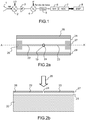
- the figure 1 schematically illustrates a conventional reception chain used in many current systems. Due to the intrinsic limitations of the bandwidth accessible by analog-to-digital converters under development, microwave reception chains require complex and costly transposition functions without any other alternative.
- the reception chain of the figure 1 comprises at the output of the microwave signal reception antenna 1 a first mixer 2 bringing the frequency of the signal back to an intermediate frequency band.
- a second mixer 4 transposes the amplified signal 3 into baseband to be sampled at high frequency by a sample-and-hold 6 after filtering 5 for example.
- the sampled signal is digitally converted by a converter 7, the digital signal being taken into account by processing means 8.
- the figures 2a and 2b present an exemplary embodiment of an optically controlled electronic switching device according to the prior art, the figure 2a representing a top view and the figure 2b a sectional view along AA '.
- the device comprises a semiconductor substrate 22, 21 on which are placed two conductive tracks 22, 23.
- the semiconductor substrate comprises for example at least two layers.
- a first layer 20 consists, for example, of semi-insulating gallium arsenide (AsGa) serving as a support. In order to obtain very short response times, this first layer is completed at the surface by a semiconductor layer, epitaxied at low temperature (AsGa BT). This last layer can also be doped.
- AsGa semi-insulating gallium arsenide
- the interaction zone 10 is therefore substantially the dimensions of the tracks and of the gap.
- the switch also has two input ports 26, 27, each port being connected to a track 22, 23.
- the ports 26, 27 for example extend the tracks.
- Two conductive strips 28, 29 arranged on each side of the conductive tracks 22, 23, and at equal distances, are connected to a ground potential thus forming ground planes.
- the switch as illustrated by figures 2a and 2b thus fits into a microwave line of the coplanar type.
- the dimensions between the central tracks 22, 23 and peripheral ground planes 28, 29 are defined so that the switch that the input or output impedance of the switch is adapted to the characteristic impedances of the standard microwave lines, that is, i.e. 50 ohms or 75 ohms as in all conventional switches.
- the length of the switch shown in figure 2 is for example of the order of 1 mm and its width of the order of 100 ⁇ m.
- the quality of the switching is characterized in particular between the contrast in the on state and the contrast in the open state, the ON / OFF contrast defined above.
- An objective of the invention is to provide a switching device whose microwave performance is optimized in the sense that they maximize this contrast, corresponding to the improvement of the signal-to-noise ratio and therefore of the switching quality.
- the optical power required for the control should preferably be minimized.
- the figures 3a and 3b illustrate an exemplary embodiment of a switching device according to the invention.
- the figure 3a presents a top view and the figure 3b a sectional view along AA '.
- the device always comprises a semiconductor substrate 20, 21, for example of the type of that of figures 2a and 2b , on which are placed conductive tracks 32, 33.
- the structure of the switch is always of the coplanar type. Two ground planes 28, 29 are therefore placed on each side of the conductive tracks 32, 33.
- the conductive tracks 32, 33 have a termination of dimension equivalent to the length of the gap, at the level of the gap.
- the width of the tracks at the level of the gap is in the same order of magnitude as the length of the gap.
- the width of the tracks is for example substantially equal to 0.5 ⁇ m.
- the input and output impedances of the switch are mismatched when the latter is in the open state.
- the contrast between the on state and the open state (ON / OFF) is increased.
- the insertion losses in the open state (OFF) are increased in this case.
- Mismatching the input and output impedances of the switch generates signal reflections at its input and output, which increases transmission losses. These losses increase the contrast between the on state and the off state by adding to the highly resistive impedance of the interaction zone. This increase in contrast between the on state and the open state however requires that the input and output impedances of the switch be matched when the switch is in the on state.
- the geometry of the conductive tracks 32, 33 makes it possible to adapt the input / output impedances of the switch to the characteristic impedances of the microwave lines to which it is connected, 50 ohms or 75 ohms for the standard lines, for the on state and to mismatch these impedances for the open state.
- the impedance of the interaction zone goes from a few kilo-ohms, in the open state, to a few tens of ohms by confinement of the illumination zone, in the on state.
- This impedance then becomes compatible with the access impedance of the tracks chosen for the mismatch in the open state (OFF), thus reducing signal reflections along the device.
- the gap is dimensioned in length and in width so that the input impedance and the output impedance of the switch are adapted to the impedance characteristic of the microwave line, for example to a standard microwave line having a characteristic impedance of 50 ohms or 75 ohms.
- the figure 4 presents, in a top view, another possible embodiment of a switch according to the invention, still in a structure of the coplanar type.
- the ground planes 48, 49 arranged on each side of the tracks 32, 33 tighten in the direction of these tracks so as to leave a space 41 of constant width, or almost, between them and the tracks.
- the figures 5a and 5b show respectively, in a top view and in a sectional view along AA ', a possible embodiment of a switch according to the invention.
- the configuration is of the microstrip type, that is to say that there is no ground plane on each side of the conductive tracks 32, 33 but a ground plane 50 located in rear face of the semi-insulating GaAs substrate.
- the figure 6 illustrates the equivalent diagram of the switch in the open state.
- the equivalent scheme is composed of three capacitors Cs, Cp1, Cp2.
- the capacitors Cp1 and Cp2 respectively represent the capacitors of the tracks 22, 33 with respect to a ground plane.
- the capacitor Cs, connected between the ends of Cp1 and Cp2, represents the capacitance of the gap of width s.
- the values of these capacitors depend on the different dimensions involved. They depend in particular on the thickness h of the semiconductor substrate, on the width s of the gap and on the geometry of the tracks 32, 33.
- the geometry of the tracks depends in particular on the point shape of the latter as illustrated by the figures 3a, 4 and 5 , and in particular by the length of the point and its maximum width.
- the input and output impedance of the switch in the open state are themselves dependent on these capacities. Dimensions are therefore defined making it possible to obtain a mismatch of the input and output impedances of the switch.
- the dimensions of the substrate and the geometry of the tracks can be easily calculated by simulation.
- a device according to the invention as described above can advantageously be incorporated into electronic components, operating at microwave frequency in particular.
- An advantageous example is that of a blocker sampler having to operate in a wide instantaneous frequency band.
- a switching device according to the invention can perform sampling at very high frequencies, while consuming little energy.
- a switching device according to the invention can provide an ON / OFF contrast greater than 30 dB at 20 GHz for example, with an optical control power reduced to 10 mW average.
- Other electronic components requiring ultra-fast switching functions can advantageously incorporate a switching device according to the invention.
Landscapes
- Waveguide Switches, Polarizers, And Phase Shifters (AREA)
Description
- La présente invention concerne un dispositif de commutation de signaux hyperfréquence, notamment de dimensions nanométriques. L'invention concerne également un composant électronique incorporant un tel dispositif. Elle s'applique notamment dans le domaine de la conversion analogique/numérique pour des applications touchant le domaine des télécommunications ou le domaine des systèmes de détection électromagnétiques. Ainsi, elle s'applique par exemple pour des récepteurs hyperfréquences fonctionnant à des fréquences correspondant aux ondes millimétriques ou à des récepteurs de bande instantanée de plusieurs gigahertz.
- Avec les nouvelles applications de ces domaines, les besoins en bande passante augmentent régulièrement tout en s'accompagnant d'une demande de réduction de coûts, et donc de simplification de la chaîne de réception des signaux RF.
- Plusieurs effets combinés mettent en relief le besoin de systèmes d'échantillonnage et de conversion de signaux analogiques en numérique.
- Afin de traiter numériquement les signaux reçus, les chaînes de réception de ces récepteurs doivent disposer de fonctions de conversion analogique-numérique.
- Ainsi, les télécommunications requièrent des bandes passantes de plus en plus élevées pour autoriser la transmission des flux denses de données dans les réseaux locaux sans fils (WLAN) notamment. On peut considérer qu'une loi équivalente à la loi de Moore apparaît pour les transmissions de données, à savoir que le débit de données des communications sans fil double tous les 18 mois, dépassant rapidement le taux de 1 Gbps.
- En raison des limitations intrinsèques de la bande passante accessible par les convertisseurs analogique/numérique en cours de développement, les chaînes de réception hyperfréquences requièrent des fonctions de transposition complexes et coûteuses sans autres alternatives technologiques suggérées à ce jour.
- En particulier, les technologies actuelles à base de semi-conducteurs ne permettent pas de disposer de codeurs analogiques-numérique fonctionnant au-delà de 2 à 3 GHz avec une dynamique élevée, souvent située au-delà de 50 dB de rapport signal sur bruit. Il est conventionnel d'introduire dans la chaîne de réception des fonctions de mélange hyperfréquence afin de transposer les signaux reçus dans la bande de fréquence compatible de l'entrée d'un codeur.
- Lorsque les fréquences d'entrée sont très élevées, il faut recourir à plusieurs étages de mélange, ce qui accroît considérablement la complexité des chaînes de réception hyperfréquences.
- Les dispositifs électroniques à commande optique peuvent être utilisés pour effectuer les fonctions de commutations ou d'échantillonnage nécessaires pour réaliser des convertisseurs notamment.
- Dans le cadre d'une utilisation dans un système de réception analogique, un utilisateur cherche généralement un dispositif dont les performances de dynamique, de pertes d'insertion et de bruit soient optimisées et dont la puissance optique de commande soit la plus faible possible. En particulier, dans le cas d'un photo-interrupteur cela se traduit par un dispositif dont les deux états commandés optiquement, l'état passant et l'état bloqué, sont très différents en niveau de transmission, cette différence étant de plusieurs dizaines de décibels (dB). Un tel interrupteur, ou commutateur, peut être défini comme un dispositif comportant deux électrodes représentant un port d'entrée et un port de sortie déposés sur un substrat photoconducteur ainsi qu'une zone d'interaction constituée par la zone du substrat qui sépare les deux ports et qui sous l'action d'une onde lumineuse assure la continuité électrique entre les deux ports. L'acheminement de l'onde lumineuse de commande jusqu'à la zone du composant sur laquelle elle interagit (zone d'interaction) pour commander le fonctionnement du composant est généralement réalisé au moyen d'une fibre optique. L'optimisation de la puissance optique de commande s'obtient par la mise en œuvre de systèmes permettant de focaliser toute la lumière dans la zone d'interaction, avec des limitations qui sont de l'ordre de 10 µm pour une fibre monomode et de 50 µm pour une fibre multi-modes. La littérature fait état de nombreuses recherches sur la réalisation de photo-interrupteurs à éclairement par une puissance optique importante ayant un mode de fonctionnement ultra rapide, les temps en jeu étant de l'ordre de la picoseconde.
- Cependant les dispositifs réalisés à ce jour présentent des caractéristiques et des performances qui limitent la fréquence d'utilisation aux fréquences compatibles du meilleur contraste entre l'état passant et l'état bloqué, noté ON/OFF. Ainsi, les dispositifs actuels sont limités à des fréquences de l'ordre de 1 à 2 GHz, leurs caractéristiques et performances étant les suivantes :
- Contraste ON/OFF faible, de l'ordre de 3 dB à 10 dB à la fréquence de 20 GHz ;
- Pertes d'insertion de l'ordre de 30 dB ;
- Puissance optique de commande élevée, de l'ordre de 100 mW moyen.
- Pour un semi-conducteur donné, la réduction de la puissance optique de commande optique exige des dimensions beaucoup plus faibles au niveau de la zone éclairée, ces dimensions étant par exemple d'ordre nanométriques.
- Un document
FR 2 908 569 - Un but de l'invention est notamment de permettre la réalisation de dispositifs de commutation électronique à commande optique de très faibles dimensions, par exemple nanométrique, améliorant l'ensemble des performances cités ci-dessus, en termes de puissance, de pertes d'insertion et de contraste. A cet effet, l'invention a pour objet un dispositif de commutation d'un signal électrique commandé par une onde optique ayant un état passant et un état ouvert tel que défini dans la revendication 1, apte à être inséré dans une ligne de transmission hyperfréquence, ledit dispositif comportant un substrat semi-conducteur sur lequel sont réalisées deux pistes conductrices séparées par un gap assurant une isolation électrique entre les deux pistes reliées chacune à un port d'entrée et de sortie, à l'état passant le contact électrique entre les deux pistes étant établi en illuminant le substrat dans la zone du gap au moyen de l'onde optique, l'impédance d'entrée et l'impédance de sortie dudit dispositif de commutation étant désadaptées à l'impédance de la ligne de transmission à l'état ouvert et sont adaptées à l'impédance de la ligne de transmission à l'état passant.
- A l'état ouvert l'impédance d'entrée et l'impédance de sortie sont par exemple supérieures à un kilo ohms.
- La largeur des pistes conductrices décroit depuis les ports d'entrée et de sortie jusqu'au gap, la décroissance pouvant être linéaire. Avantageusement, les pistes ont par exemple une terminaison au niveau du gap de dimension équivalente à longueur du gap.
- La structure du dispositif étant du type coplanaire, il comporte par exemple un plan de masse de chaque côté des pistes conductrices, la distance entre les plans de masse et les pistes restant sensiblement constante entre les ports d'entrée et de sortie et le gap.
- La longueur du gap est par exemple inférieure à 1µm, elle peut être de l'ordre de 0,5 µm.
- L'invention a également pour objet un composant électronique incorporant un dispositif selon l'invention tel que décrit précédemment. En particulier, un tel composant peut être un échantillonneur bloqueur.
- D'autres caractéristiques et avantages de l'invention apparaîtront à l'aide de la description qui suit faite en regard de dessins annexés qui représentent :
- la
figure 1 , une illustration schématique d'une chaîne de réception ; - les
figures 2a et 2b , un exemple de dispositif de commutation à commande optique selon l'art antérieur ; - les
figures 3a et 3b , un exemple de dispositif de commutation à commande optique selon l'invention ; - la
figure 4 , un autre exemple de réalisation d'un dispositif selon l'invention dans une structure de type coplanaire avec resserrement des masses ; - la
figure 5 , un exemple de réalisation d'un dispositif selon l'invention dans une structure de type microruban ; - la
figure 6 , un schéma équivalent d'un exemple de réalisation d'un dispositif selon l'invention à l'état ouvert illustrant le calcul des dimensions dudit dispositif. - La
figure 1 illustre, de façon schématique, une chaîne de réception classique, utilisé dans de nombreux systèmes actuels. En raison des limitations intrinsèque de la bande passante accessible par les convertisseurs analogique-numérique en cours de développement, les chaînes de réception hyperfréquence requièrent des fonctions de transposition complexes et coûteuses sans autre alternative. Ainsi, la chaîne de réception de lafigure 1 comporte en sortie de l'antenne de réception 1 du signal hyperfréquence un premier mélangeur 2 ramenant la fréquence du signal dans une bande de fréquence intermédiaire. Un deuxième mélangeur 4 transpose le signal amplifié 3 en bande de base pour être échantillonné en haute fréquence par un échantillonneur-bloqueur 6 après filtrage 5 par exemple. Le signal échantillonné est converti numériquement par un convertisseur 7, le signal numérique étant pris en compte par des moyens de traitement 8. - Les systèmes futurs, encore plus que les systèmes actuels, nécessiteront de réaliser des récepteurs fonctionnant soit à très haute fréquence, à plusieurs dizaines de GHz, soit à très large bande passante instantanée, par exemple 20 GHz. De tels récepteurs nécessitent des fonctions de commutations très performantes. Des dispositifs de commutations à commande optique, capables de commuter très rapidement, peuvent répondre à ces fréquences de fonctionnement à conditions qu'ils présentent des performances suffisantes au niveau du contraste ON/OFF, supérieur à 50 dB par exemple. Il faut aussi qu'ils présentent des performances suffisantes en ce qui concerne la puissance optique nécessaire et les pertes d'insertions pour permettre un fonctionnement acceptable en termes de consommation d'énergie. De tels commutateurs constituent une fonction de commutation élémentaire pour des composants de la chaîne de réception, tels que les échantillonneurs-bloqueurs par exemple. Ils peuvent aussi être utilisés pour réaliser des mélangeurs, des déphaseurs et autres composants nécessitant une fonction de commutation élémentaire ultrarapide performante.
- Les
figures 2a et 2b présentent un exemple de réalisation d'un dispositif de commutation électronique à commande optique selon l'art antérieur, lafigure 2a représentant une vue de dessus et lafigure 2b une vue en coupe selon AA'. Le dispositif comporte un substrat semi-conducteur 22, 21 sur lequel sont placées deux pistes conductrices 22, 23. Le substrat semi-conducteur comporte par exemple au moins deux couches. Une première couche 20 est par exemple constituée d'arséniure de gallium (AsGa) semi-isolant servant de support. Afin d'obtenir des temps de réponse très courts, cette première couche est complétée en surface par une couche de semi-conducteur, épitaxiée à basse température (AsGa BT). Cette dernière couche peut par ailleurs être dopée. - Les pistes conductrices 22, 23 sont placées en alignement et séparées par un espace 24, appelé encore gap, ne portant pas de métallisation de façon à être isolées électriquement l'une de l'autre. Pour réaliser la fonction de commutation on apporte au substrat de l'énergie au moyen d'une onde lumineuse 25. Cet apport d'énergie a pour conséquence de rendre le substrat localement conducteur dans la zone éclairée 10 par injonction de porteurs dans cette zone, zone qui englobe le gap 24 séparant les deux pistes conductrices 22, 23. Cette zone 10 est encore appelée zone d'interaction. Une continuité électrique est ainsi établie entre ces deux pistes, correspondant à l'état passant du commutateur. Inversement si la zone d'interaction 10 cesse d'être éclairée, elle cesse par là même d'être conductrice et la continuité électrique est interrompue, le commutateur étant alors à l'état ouvert. Des dimensions typiques peuvent être les suivantes :
- Longueur du gap 24 = 10 µm
- Largeur d'une piste 22, 23 = 10 µm
- Diamètre de la zone éclairée, zone d'interaction 10 = 10 µm
- La zone d'interaction 10 est donc sensiblement aux dimensions des pistes et du gap.
- Le commutateur comporte par ailleurs deux ports d'entrée 26, 27, chaque port étant relié à une piste 22, 23. En pratique, les ports 26, 27 prolongent par exemple les pistes. Deux bandes conductrices 28,29 disposées de chaque côté des pistes conductrices 22, 23, et à égales distances, sont reliées à un potentiel de masse formant ainsi des plans de masse. Le commutateur tel qu'illustré par les
figures 2a et 2b s'inscrit ainsi dans une ligne hyperfréquence du type coplanaire. Les dimensions entre les pistes centrales 22, 23 et plans de masse périphérique 28, 29 sont définies de telle sorte que le commutateur que l'impédance d'entrée ou de sortie du commutateur soit adaptée aux impédances caractéristiques des lignes hyperfréquence standards, c'est-à-dire 50 ohms ou 75 ohms comme dans tous les commutateurs classiques. La longueur du commutateur présenté enfigure 2 est par exemple de l'ordre de 1 mm et sa largeur de l'ordre 100 µm. La qualité de la commutation est notamment caractérisée entre le contraste à l'état passant et le contraste à l'état ouvert, contraste ON/OFF défini précédemment. Un objectif de l'invention est de réaliser un dispositif de commutation dont les performances hyperfréquence sont optimisées dans le sens qu'elles maximisent ce contraste, correspondant à l'amélioration du rapport signal sur bruit et donc de la qualité de commutation. Par ailleurs, la puissance optique nécessaire à la commande doit être de préférence minimisée. - Les
figures 3a et 3b illustrent un exemple de réalisation d'un dispositif de commutation selon l'invention. Comme pour lesfigures 2a et 2b , lafigure 3a présente une vue de dessus et lafigure 3b une vue en coupe selon AA'. Le dispositif comporte toujours un substrat semi-conducteur 20, 21, par exemple du type de celui desfigures 2a et 2b , sur lequel sont placées des pistes conductrices 32, 33. La structure du commutateur est toujours du type coplanaire. Deux plans de masse 28, 29 sont donc placées de chaque côté des pistes conductrices 32,33. - Selon l'invention, ces pistes conductrices 32, 33 ont un profil particulier. Partant des ports d'entrée 36, 37, elles décroissent en largeur jusqu'à finir par exemple en pointe au niveau du gap 34 séparant ces deux pistes. Comme dans le cas précédent, un faisceau optique 35 éclaire une zone 100 englobant ce gap 34. Dans cet exemple de réalisation, les dimensions typiques peuvent être les suivantes :
- Longueur du gap 34 = 0,5 µm
- Diamètre de la zone éclairée, zone d'interaction 100 = 1 à 2 µm
- Largeur d'une piste conductrice 32, 33 au niveau du gap : elle est inférieure à 1 µm.
- Ces grandeurs montrent dans cet exemple de réalisation, les pistes conductrices 32, 33 ont une terminaison de dimension équivalente à la longueur du gap, au niveau du gap. En d'autres termes, la largeur des pistes au niveau du gap est dans le même ordre de grandeur que la longueur du gap. La largeur des pistes est par exemple sensiblement égale à 0,5 µm. Pour obtenir une zone d'interaction 100 de si faible diamètre et donc confiner le faisceau dans une si faible surface, on dispose de moyen pour guider et focaliser le faisceau lumineux 35 vers cette zone 100.
- Par ailleurs selon l'invention, les impédances d'entrée et de sortie du commutateur sont désadaptées lorsque celui-ci est à l'état ouvert. Ainsi le contraste entre l'état passant et l'état ouvert (ON/OFF) est augmenté. En effet, on augmente dans ce cas les pertes d'insertion à l'état ouvert (OFF). La désadaptation des impédances d'entrée et de sortie du commutateur génère des réflexions de signal à son entrée et à sa sortie, ce qui augmente les pertes en transmission. Ces pertes augmentent le contraste entre l'état passant et l'état bloqué en s'ajoutant à l'impédance hautement résistive de la zone d'interaction. Cette augmentation de contraste entre l'état passant et l'état ouvert exige cependant que les impédances d'entrée et de sortie du commutateur soient adaptées lorsque celui est à l'état passant.
- La géométrie des pistes conductrices 32, 33 permet d'adapter les impédances d'entrée/sortie du commutateur aux impédances caractéristiques des lignes hyperfréquence auxquelles il est relié, 50 ohms ou 75 ohms pour les lignes standard, pour l'état passant et de désadapter ces impédances pour l'état ouvert.
- Ainsi, un commutateur selon l'invention est tel que :
- l'impédance d'entrée/sortie du commutateur est désadaptée à l'impédance de la ligne de transmission interrompue en absence de commande optique correspondant à l'état ouvert ;
- l'impédance d'entrée/sortie du commutateur est adaptée à l'impédance de la ligne de transmission à l'état passant, plus particulièrement l'impédance de ligne est adaptée à la résistance créée par l'éclairement de la zone d'interaction 100.
- Lors de l'éclairement, l'impédance de la zone d'interaction passe de quelques kilo-ohms, à l'état ouvert, à quelques dizaines d'ohms par confinement de la zone d'éclairement, à l'état passant. Cette impédance devient alors compatible avec l'impédance d'accès des pistes choisie pour la désadaptation à l'état ouvert (OFF), réduisant ainsi les réflexions de signaux le long du dispositif. Plus particulièrement, le gap est dimensionné en longueur et en largeur pour que l'impédance d'entrée et l'impédance de sortie du commutateur soit adaptée à l'impédance caractéristique de la ligne hyperfréquence, par exemple à une ligne hyperfréquence standard ayant une impédance caractéristique de 50 ohms ou 75 ohms. En pratique, il suffit que l'impédance d'entrée et l'impédance de sortie s'approchent de ces valeurs, c'est-à-dire soit de l'ordre de quelques dizaines d'ohms.
- La
figure 4 présente, par une vue de dessus un autre mode de réalisation possible d'un commutateur selon l'invention, toujours dans une structure du type coplanaire. Dans ce mode de réalisation, les plans de masse 48, 49 disposés de chaque côté des pistes 32, 33 se resserrent en direction de ces pistes de façon à laisser un espace 41 de largeur constante, ou presque, entre elles et les pistes. - Les
figures 5a et 5b présentent respectivement, par une vue de dessus et par une vue en coupe selon AA', un mode de réalisation possible d'un commutateur selon l'invention. Dans cet exemple de réalisation, la configuration est de type micro ruban, c'est-à-dire qu'il n'y a pas de plan de masse de chaque côté des pistes conductrices 32, 33 mais un plan de masse 50 situé en face arrière du substrat de GaAs semi-isolant. - La
figure 6 illustre le schéma équivalent de l'interrupteur à l'état ouvert. Le schéma équivalent est composé de trois capacités Cs, Cp1, Cp2. Les capacités Cp1 et Cp2 représentent respectivement les capacités des pistes 22, 33 par rapport à un plan de masse. La capacité Cs, connectée entre les extrémités de Cp1 et Cp2, représente la capacité du gap de largeur s. Les valeurs de ces capacités dépendent des différentes dimensions en jeu. Elles dépendent notamment de l'épaisseur h du substrat semi-conducteur, de la largeur s du gap et de la géométrie des pistes 32, 33. La géométrie des pistes dépend notamment de la forme en pointe de ces dernières telle qu'illustrée par lesfigures 3a, 4 et5 , et notamment par la longueur de la pointe et sa largeur maximum. - L'impédance d'entrée et de sortie du commutateur à l'état ouvert sont elles-mêmes dépendante de ces capacités. On définit donc des dimensions permettant d'obtenir une désadaptation des impédances d'entrée et de sortie du commutateur.
- Un autre paramètre de dimensionnement est la valeur de l'impédance d'entrée du commutateur à l'état passant. Celle-ci est adaptée à la ligne. Dans ce cas, la capacité Cs du schéma équivalent de la
figure 6 est remplacée par une résistance que l'on peut calculer notamment en fonction de la largeur de gap s et de la largeur du flux de courant électrique créé lors de l'éclairement de la zone de gap. On peut ainsi définir des dimensions et une géométrie des pistes conductrices en fonction des contraintes imposées, notamment : - largeur du gap inférieur à 1 µm par exemple ;
- adaptation de l'impédance d'entrée à l'état passant et ;
- désadaptation complète à l'état ouvert.
- Les dimensions du substrat et la géométrie des pistes peuvent être aisément calculées par simulation.
- Un dispositif selon l'invention tel que décrit précédemment peut avantageusement être incorporé dans des composants électroniques, fonctionnant en hyperfréquence notamment. Un exemple avantageux est celui d'un échantillonneur bloqueur devant fonctionner dans une large bande de fréquence instantanée. En incorporant un ou plusieurs dispositifs de commutation selon l'invention, il peut effectuer des échantillonnages à très hautes fréquences, tout en consommant peu d'énergie. En effet, un dispositif de commutation selon l'invention peut assurer un contraste ON/OFF supérieur à 30 dB à 20 GHz par exemple, avec une puissance optique de commande réduite à 10 mW moyen. D'autres composants électroniques nécessitant des fonctions de commutation ultra rapide peuvent avantageusement incorporer un dispositif de commutation selon l'invention.
Claims (9)
- Dispositif de commutation d'un signal électrique commandé par une onde optique (35) ayant un état passant et un état ouvert, apte à être inséré dans une ligne de transmission hyperfréquence, ledit dispositif comportant un substrat semi-conducteur (20, 21) sur lequel sont réalisées deux pistes conductrices (32, 33) séparées par un gap (34) assurant une isolation électrique entre les deux pistes reliées chacune à un port d'entrée et de sortie (36, 37), lesdites pistes conductrices (32,33) finissant au niveau dudit gap (34), la largeur des pistes conductrices (32, 33) décroissant depuis les ports d'entrée et de sortie (36, 37) jusqu'audit gap (34), à l'état passant le contact électrique entre les deux pistes étant établi en illuminant le substrat dans la zone (100) du gap au moyen de l'onde optique, caractérisé en ce que la géométrie desdites pistes conductrices (32, 33) est définie de façon à ce que l'impédance d'entrée et l'impédance de sortie dudit dispositif de commutation créées par l'éclairement de ladite zone (100) soient adaptées à l'impédance de ladite ligne de transmission, ladite impédance d'entrée et ladite impédance de sortie soient désadaptées à ladite ligne de transmission en absence d'éclairement de ladite zone (100).
- Dispositif selon la revendication 1, caractérisé en ce qu'à l'état ouvert l'impédance d'entrée et l'impédance de sortie sont supérieures à un kilo ohms.
- Dispositif selon l'une quelconque des revendications précédentes, caractérisé en ce que ladite largeur décroit de façon linéaire.
- Dispositif selon l'une quelconque des revendications précédentes, caractérisé en ce que les pistes ont une terminaison au niveau du gap de dimension équivalente à longueur du gap.
- Dispositif selon l'une quelconque des revendications précédentes, caractérisé en ce que sa structure étant du type coplanaire, il comporte un plan de masse (28, 48) de chaque côté des pistes conductrices (32,33), la distance entre les plans de masse et les pistes restant sensiblement constant entre les ports d'entrée et de sortie et le gap.
- Dispositif selon l'une quelconque des revendications précédentes, caractérisé en ce que la longueur du gap est inférieure à 1µm
- Dispositif selon la revendication 5, caractérisé en ce que la longueur du gap est de l'ordre de 0,5 µm.
- Composant électronique, caractérisé en ce qu'il incorpore un dispositif selon l'une quelconque des revendications précédentes.
- Composant électronique selon la revendication 8, caractérisé en ce qu'il réalise la fonction d'échantillonneur bloqueur (6).
Applications Claiming Priority (2)
| Application Number | Priority Date | Filing Date | Title |
|---|---|---|---|
| FR1203563A FR3000327B1 (fr) | 2012-12-21 | 2012-12-21 | Dispositif de commutation de signaux hyperfrequences notamment de dimensions nanometriques, et composant electronique incorporant un tel dispositif |
| PCT/EP2013/077859 WO2014096431A1 (fr) | 2012-12-21 | 2013-12-20 | Dispositif de commutation de signaux hyperfrequences notamment de dimensions nanometriques, et composant electronique incorporant un tel dispositif |
Publications (2)
| Publication Number | Publication Date |
|---|---|
| EP2936682A1 EP2936682A1 (fr) | 2015-10-28 |
| EP2936682B1 true EP2936682B1 (fr) | 2021-01-20 |
Family
ID=48539226
Family Applications (1)
| Application Number | Title | Priority Date | Filing Date |
|---|---|---|---|
| EP13827008.7A Not-in-force EP2936682B1 (fr) | 2012-12-21 | 2013-12-20 | Dispositif de commutation de signaux hyperfrequences notamment de dimensions nanometriques, et composant electronique incorporant un tel dispositif |
Country Status (5)
| Country | Link |
|---|---|
| US (1) | US9548413B2 (fr) |
| EP (1) | EP2936682B1 (fr) |
| ES (1) | ES2865128T3 (fr) |
| FR (1) | FR3000327B1 (fr) |
| WO (1) | WO2014096431A1 (fr) |
Families Citing this family (1)
| Publication number | Priority date | Publication date | Assignee | Title |
|---|---|---|---|---|
| FR3073087B1 (fr) * | 2017-10-30 | 2019-09-27 | Thales | Commutateur |
Family Cites Families (5)
| Publication number | Priority date | Publication date | Assignee | Title |
|---|---|---|---|---|
| JPH09198978A (ja) * | 1996-01-23 | 1997-07-31 | Advantest Corp | 光導電スイッチ |
| US20020113759A1 (en) * | 2001-02-16 | 2002-08-22 | Levine Jules D. | Telecommunications switching array using optoelectronic display addressing |
| JP4721416B2 (ja) * | 2005-09-05 | 2011-07-13 | キヤノン株式会社 | 検体検査素子、及び検体検査装置 |
| GB2438445A (en) * | 2006-05-26 | 2007-11-28 | Thales Holdings Uk Plc | A sample-and-hold circuit for microwave signals, using photoconductive switches |
| FR2908569B1 (fr) * | 2006-11-10 | 2009-01-23 | Thales Sa | Dispositif pour confiner l'onde optique de commande dans la zone active d'un dispositif electronique a commande optique |
-
2012
- 2012-12-21 FR FR1203563A patent/FR3000327B1/fr not_active Expired - Fee Related
-
2013
- 2013-12-20 WO PCT/EP2013/077859 patent/WO2014096431A1/fr not_active Ceased
- 2013-12-20 EP EP13827008.7A patent/EP2936682B1/fr not_active Not-in-force
- 2013-12-20 ES ES13827008T patent/ES2865128T3/es active Active
- 2013-12-20 US US14/652,771 patent/US9548413B2/en not_active Expired - Fee Related
Non-Patent Citations (1)
| Title |
|---|
| None * |
Also Published As
| Publication number | Publication date |
|---|---|
| US9548413B2 (en) | 2017-01-17 |
| FR3000327B1 (fr) | 2016-02-05 |
| US20150349183A1 (en) | 2015-12-03 |
| WO2014096431A1 (fr) | 2014-06-26 |
| ES2865128T3 (es) | 2021-10-15 |
| FR3000327A1 (fr) | 2014-06-27 |
| EP2936682A1 (fr) | 2015-10-28 |
Similar Documents
| Publication | Publication Date | Title |
|---|---|---|
| EP0078187B1 (fr) | Dispositif mélangeur subharmonique hyperfréquence, et utilisation d'un tel dispositif dans un circuit hyperfréquence à transposition de fréquence | |
| EP1427053B1 (fr) | Coupleur directif | |
| FR2467488A1 (fr) | Dispositif combinateur/diviseur micro-ondes a trois voies, adapte pour des resistances d'isolement externes | |
| EP2184803B1 (fr) | Ligne à retard bi-ruban différentielle coplanaire, filtre différentiel d'ordre supérieur et antenne filtrante munis d'une telle ligne | |
| EP0013222A1 (fr) | Déphaseur hyperfréquence à diodes et antenne à balayage électronique comportant un tel déphaseur | |
| EP2184801A1 (fr) | Dispositif de filtrage différentiel à résonateurs couplés coplanaires et antenne filtrante munie d'un tel dispositif | |
| WO1991019329A1 (fr) | Ligne de transmission en mode a ondes lentes, du type microruban et circuit incluant une telle ligne | |
| EP2178152A1 (fr) | Dispositif de commutation électronique pour signaux a haute fréquence | |
| EP2202838A1 (fr) | Condensateur commuté compact mems | |
| FR2970129A1 (fr) | Filtre variable par condensateur commute au moyen de composants mems | |
| WO2014096431A1 (fr) | Dispositif de commutation de signaux hyperfrequences notamment de dimensions nanometriques, et composant electronique incorporant un tel dispositif | |
| EP2802036A1 (fr) | Déphaseur passif à déplacement longitudinal | |
| FR2831734A1 (fr) | Dispositif pour la reception et/ou l'emission de signaux electromagnetiques a diversite de rayonnement | |
| EP0335788B1 (fr) | Circuit déphaseur hyperfréquence | |
| EP2147478B1 (fr) | Coupleur de signaux hyperfrequences en technologie microruban | |
| EP2862022B1 (fr) | Composant hyperfréquence commandé par un système d'électrodes coplanaires blindées, et procédé de fabrication correspondant | |
| EP0380397B1 (fr) | Modulateur équilibré pour signal électromagnétique hyperfréquence de puissance | |
| EP0286464A1 (fr) | Dispositif hyperfréquence à diodes comportant une ligne triplaque | |
| FR3067173A1 (fr) | Composant micro-ondes presentant une chambre asymetrique de propagation | |
| EP1387409B1 (fr) | Commutateur optoélectronique ultra rapide à grand pouvoir d'isolement et large bande passante | |
| FR2859315A1 (fr) | Antenne planaire multibandes | |
| EP3477709B1 (fr) | Commutateur | |
| FR2628571A1 (fr) | Filtre coupe-bande hyperfrequence en technologie micro-bande | |
| EP1715597B1 (fr) | Antenne à surfaces rayonnantes planes à circuit commutable | |
| FR3129037A1 (fr) | Dispositif de filtrage reconfigurable et système d'acquisition de signaux radiofréquences intégrant un tel dispositif de filtrage |
Legal Events
| Date | Code | Title | Description |
|---|---|---|---|
| PUAI | Public reference made under article 153(3) epc to a published international application that has entered the european phase |
Free format text: ORIGINAL CODE: 0009012 |
|
| 17P | Request for examination filed |
Effective date: 20150617 |
|
| AK | Designated contracting states |
Kind code of ref document: A1 Designated state(s): AL AT BE BG CH CY CZ DE DK EE ES FI FR GB GR HR HU IE IS IT LI LT LU LV MC MK MT NL NO PL PT RO RS SE SI SK SM TR |
|
| AX | Request for extension of the european patent |
Extension state: BA ME |
|
| DAX | Request for extension of the european patent (deleted) | ||
| STAA | Information on the status of an ep patent application or granted ep patent |
Free format text: STATUS: EXAMINATION IS IN PROGRESS |
|
| 17Q | First examination report despatched |
Effective date: 20190508 |
|
| GRAP | Despatch of communication of intention to grant a patent |
Free format text: ORIGINAL CODE: EPIDOSNIGR1 |
|
| STAA | Information on the status of an ep patent application or granted ep patent |
Free format text: STATUS: GRANT OF PATENT IS INTENDED |
|
| INTG | Intention to grant announced |
Effective date: 20200908 |
|
| RIN1 | Information on inventor provided before grant (corrected) |
Inventor name: DECOSTER, DIDIER Inventor name: CHAZELAS, JEAN Inventor name: TRIPON-CANSELIET, CHARLOTTE |
|
| GRAS | Grant fee paid |
Free format text: ORIGINAL CODE: EPIDOSNIGR3 |
|
| GRAA | (expected) grant |
Free format text: ORIGINAL CODE: 0009210 |
|
| STAA | Information on the status of an ep patent application or granted ep patent |
Free format text: STATUS: THE PATENT HAS BEEN GRANTED |
|
| AK | Designated contracting states |
Kind code of ref document: B1 Designated state(s): AL AT BE BG CH CY CZ DE DK EE ES FI FR GB GR HR HU IE IS IT LI LT LU LV MC MK MT NL NO PL PT RO RS SE SI SK SM TR |
|
| REG | Reference to a national code |
Ref country code: GB Ref legal event code: FG4D Free format text: NOT ENGLISH |
|
| REG | Reference to a national code |
Ref country code: CH Ref legal event code: EP |
|
| REG | Reference to a national code |
Ref country code: AT Ref legal event code: REF Ref document number: 1357236 Country of ref document: AT Kind code of ref document: T Effective date: 20210215 |
|
| REG | Reference to a national code |
Ref country code: IE Ref legal event code: FG4D Free format text: LANGUAGE OF EP DOCUMENT: FRENCH |
|
| REG | Reference to a national code |
Ref country code: DE Ref legal event code: R096 Ref document number: 602013075418 Country of ref document: DE |
|
| RAP2 | Party data changed (patent owner data changed or rights of a patent transferred) |
Owner name: SORBONNE UNIVERSITE Owner name: UNIVERSITE DES SCIENCES ET TECHNOLOGIES DE LILLE Owner name: THALES |
|
| RAP2 | Party data changed (patent owner data changed or rights of a patent transferred) |
Owner name: SORBONNE UNIVERSITE Owner name: UNIVERSITE DE LILLE Owner name: THALES |
|
| REG | Reference to a national code |
Ref country code: NL Ref legal event code: MP Effective date: 20210120 |
|
| REG | Reference to a national code |
Ref country code: LT Ref legal event code: MG9D |
|
| REG | Reference to a national code |
Ref country code: AT Ref legal event code: MK05 Ref document number: 1357236 Country of ref document: AT Kind code of ref document: T Effective date: 20210120 |
|
| REG | Reference to a national code |
Ref country code: DE Ref legal event code: R081 Ref document number: 602013075418 Country of ref document: DE Owner name: UNIVERSITE DES SCIENCES ET TECHNOLOGIES DE LIL, FR Free format text: FORMER OWNERS: THALES, COURBEVOIE, FR; UNIVERSITE DES SCIENCES ET TECHNOLOGIES DE LILLE, VILLENEUVE D'ASCQ, FR; UNIVERSITE PARIS 6 PIERRE ET MARIE CURIE UPMC, PARIS, FR Ref country code: DE Ref legal event code: R081 Ref document number: 602013075418 Country of ref document: DE Owner name: THALES, FR Free format text: FORMER OWNERS: THALES, COURBEVOIE, FR; UNIVERSITE DES SCIENCES ET TECHNOLOGIES DE LILLE, VILLENEUVE D'ASCQ, FR; UNIVERSITE PARIS 6 PIERRE ET MARIE CURIE UPMC, PARIS, FR Ref country code: DE Ref legal event code: R081 Ref document number: 602013075418 Country of ref document: DE Owner name: SORBONNE UNIVERSITE, FR Free format text: FORMER OWNERS: THALES, COURBEVOIE, FR; UNIVERSITE DES SCIENCES ET TECHNOLOGIES DE LILLE, VILLENEUVE D'ASCQ, FR; UNIVERSITE PARIS 6 PIERRE ET MARIE CURIE UPMC, PARIS, FR |
|
| PG25 | Lapsed in a contracting state [announced via postgrant information from national office to epo] |
Ref country code: HR Free format text: LAPSE BECAUSE OF FAILURE TO SUBMIT A TRANSLATION OF THE DESCRIPTION OR TO PAY THE FEE WITHIN THE PRESCRIBED TIME-LIMIT Effective date: 20210120 Ref country code: GR Free format text: LAPSE BECAUSE OF FAILURE TO SUBMIT A TRANSLATION OF THE DESCRIPTION OR TO PAY THE FEE WITHIN THE PRESCRIBED TIME-LIMIT Effective date: 20210421 Ref country code: FI Free format text: LAPSE BECAUSE OF FAILURE TO SUBMIT A TRANSLATION OF THE DESCRIPTION OR TO PAY THE FEE WITHIN THE PRESCRIBED TIME-LIMIT Effective date: 20210120 Ref country code: PT Free format text: LAPSE BECAUSE OF FAILURE TO SUBMIT A TRANSLATION OF THE DESCRIPTION OR TO PAY THE FEE WITHIN THE PRESCRIBED TIME-LIMIT Effective date: 20210520 Ref country code: LT Free format text: LAPSE BECAUSE OF FAILURE TO SUBMIT A TRANSLATION OF THE DESCRIPTION OR TO PAY THE FEE WITHIN THE PRESCRIBED TIME-LIMIT Effective date: 20210120 Ref country code: BG Free format text: LAPSE BECAUSE OF FAILURE TO SUBMIT A TRANSLATION OF THE DESCRIPTION OR TO PAY THE FEE WITHIN THE PRESCRIBED TIME-LIMIT Effective date: 20210420 Ref country code: NO Free format text: LAPSE BECAUSE OF FAILURE TO SUBMIT A TRANSLATION OF THE DESCRIPTION OR TO PAY THE FEE WITHIN THE PRESCRIBED TIME-LIMIT Effective date: 20210420 Ref country code: NL Free format text: LAPSE BECAUSE OF FAILURE TO SUBMIT A TRANSLATION OF THE DESCRIPTION OR TO PAY THE FEE WITHIN THE PRESCRIBED TIME-LIMIT Effective date: 20210120 |
|
| PG25 | Lapsed in a contracting state [announced via postgrant information from national office to epo] |
Ref country code: LV Free format text: LAPSE BECAUSE OF FAILURE TO SUBMIT A TRANSLATION OF THE DESCRIPTION OR TO PAY THE FEE WITHIN THE PRESCRIBED TIME-LIMIT Effective date: 20210120 Ref country code: RS Free format text: LAPSE BECAUSE OF FAILURE TO SUBMIT A TRANSLATION OF THE DESCRIPTION OR TO PAY THE FEE WITHIN THE PRESCRIBED TIME-LIMIT Effective date: 20210120 Ref country code: PL Free format text: LAPSE BECAUSE OF FAILURE TO SUBMIT A TRANSLATION OF THE DESCRIPTION OR TO PAY THE FEE WITHIN THE PRESCRIBED TIME-LIMIT Effective date: 20210120 Ref country code: AT Free format text: LAPSE BECAUSE OF FAILURE TO SUBMIT A TRANSLATION OF THE DESCRIPTION OR TO PAY THE FEE WITHIN THE PRESCRIBED TIME-LIMIT Effective date: 20210120 Ref country code: SE Free format text: LAPSE BECAUSE OF FAILURE TO SUBMIT A TRANSLATION OF THE DESCRIPTION OR TO PAY THE FEE WITHIN THE PRESCRIBED TIME-LIMIT Effective date: 20210120 |
|
| PG25 | Lapsed in a contracting state [announced via postgrant information from national office to epo] |
Ref country code: IS Free format text: LAPSE BECAUSE OF FAILURE TO SUBMIT A TRANSLATION OF THE DESCRIPTION OR TO PAY THE FEE WITHIN THE PRESCRIBED TIME-LIMIT Effective date: 20210520 |
|
| REG | Reference to a national code |
Ref country code: ES Ref legal event code: FG2A Ref document number: 2865128 Country of ref document: ES Kind code of ref document: T3 Effective date: 20211015 |
|
| REG | Reference to a national code |
Ref country code: DE Ref legal event code: R097 Ref document number: 602013075418 Country of ref document: DE |
|
| PG25 | Lapsed in a contracting state [announced via postgrant information from national office to epo] |
Ref country code: EE Free format text: LAPSE BECAUSE OF FAILURE TO SUBMIT A TRANSLATION OF THE DESCRIPTION OR TO PAY THE FEE WITHIN THE PRESCRIBED TIME-LIMIT Effective date: 20210120 Ref country code: CZ Free format text: LAPSE BECAUSE OF FAILURE TO SUBMIT A TRANSLATION OF THE DESCRIPTION OR TO PAY THE FEE WITHIN THE PRESCRIBED TIME-LIMIT Effective date: 20210120 Ref country code: SM Free format text: LAPSE BECAUSE OF FAILURE TO SUBMIT A TRANSLATION OF THE DESCRIPTION OR TO PAY THE FEE WITHIN THE PRESCRIBED TIME-LIMIT Effective date: 20210120 |
|
| REG | Reference to a national code |
Ref country code: DE Ref legal event code: R081 Ref document number: 602013075418 Country of ref document: DE Owner name: THALES, FR Free format text: FORMER OWNERS: SORBONNE UNIVERSITE, PARIS, FR; THALES, COURBEVOIE, FR; UNIVERSITE DE LILLE, LILLE, FR Ref country code: DE Ref legal event code: R081 Ref document number: 602013075418 Country of ref document: DE Owner name: SORBONNE UNIVERSITE, FR Free format text: FORMER OWNERS: SORBONNE UNIVERSITE, PARIS, FR; THALES, COURBEVOIE, FR; UNIVERSITE DE LILLE, LILLE, FR Ref country code: DE Ref legal event code: R081 Ref document number: 602013075418 Country of ref document: DE Owner name: THALES, FR Free format text: FORMER OWNERS: SORBONNE UNIVERSITE, PARIS, FR; THALES, COURBEVOIE, FR; UNIVERSITE DES SCIENCES ET TECHNOLOGIES DE LILLE, VILLENEUVE D'ASCQ, FR Ref country code: DE Ref legal event code: R081 Ref document number: 602013075418 Country of ref document: DE Owner name: SORBONNE UNIVERSITE, FR Free format text: FORMER OWNERS: SORBONNE UNIVERSITE, PARIS, FR; THALES, COURBEVOIE, FR; UNIVERSITE DES SCIENCES ET TECHNOLOGIES DE LILLE, VILLENEUVE D'ASCQ, FR |
|
| RAP2 | Party data changed (patent owner data changed or rights of a patent transferred) |
Owner name: SORBONNE UNIVERSITE Owner name: THALES |
|
| PLBE | No opposition filed within time limit |
Free format text: ORIGINAL CODE: 0009261 |
|
| STAA | Information on the status of an ep patent application or granted ep patent |
Free format text: STATUS: NO OPPOSITION FILED WITHIN TIME LIMIT |
|
| PG25 | Lapsed in a contracting state [announced via postgrant information from national office to epo] |
Ref country code: SK Free format text: LAPSE BECAUSE OF FAILURE TO SUBMIT A TRANSLATION OF THE DESCRIPTION OR TO PAY THE FEE WITHIN THE PRESCRIBED TIME-LIMIT Effective date: 20210120 Ref country code: RO Free format text: LAPSE BECAUSE OF FAILURE TO SUBMIT A TRANSLATION OF THE DESCRIPTION OR TO PAY THE FEE WITHIN THE PRESCRIBED TIME-LIMIT Effective date: 20210120 Ref country code: DK Free format text: LAPSE BECAUSE OF FAILURE TO SUBMIT A TRANSLATION OF THE DESCRIPTION OR TO PAY THE FEE WITHIN THE PRESCRIBED TIME-LIMIT Effective date: 20210120 |
|
| 26N | No opposition filed |
Effective date: 20211021 |
|
| REG | Reference to a national code |
Ref country code: GB Ref legal event code: 732E Free format text: REGISTERED BETWEEN 20211230 AND 20220105 |
|
| PG25 | Lapsed in a contracting state [announced via postgrant information from national office to epo] |
Ref country code: AL Free format text: LAPSE BECAUSE OF FAILURE TO SUBMIT A TRANSLATION OF THE DESCRIPTION OR TO PAY THE FEE WITHIN THE PRESCRIBED TIME-LIMIT Effective date: 20210120 |
|
| PGFP | Annual fee paid to national office [announced via postgrant information from national office to epo] |
Ref country code: GB Payment date: 20211118 Year of fee payment: 9 Ref country code: DE Payment date: 20211116 Year of fee payment: 9 Ref country code: FR Payment date: 20211126 Year of fee payment: 9 |
|
| REG | Reference to a national code |
Ref country code: GB Ref legal event code: 732E Free format text: REGISTERED BETWEEN 20220106 AND 20220112 |
|
| PG25 | Lapsed in a contracting state [announced via postgrant information from national office to epo] |
Ref country code: SI Free format text: LAPSE BECAUSE OF FAILURE TO SUBMIT A TRANSLATION OF THE DESCRIPTION OR TO PAY THE FEE WITHIN THE PRESCRIBED TIME-LIMIT Effective date: 20210120 |
|
| PGFP | Annual fee paid to national office [announced via postgrant information from national office to epo] |
Ref country code: IT Payment date: 20211129 Year of fee payment: 9 |
|
| PG25 | Lapsed in a contracting state [announced via postgrant information from national office to epo] |
Ref country code: IS Free format text: LAPSE BECAUSE OF FAILURE TO SUBMIT A TRANSLATION OF THE DESCRIPTION OR TO PAY THE FEE WITHIN THE PRESCRIBED TIME-LIMIT Effective date: 20210520 |
|
| PGFP | Annual fee paid to national office [announced via postgrant information from national office to epo] |
Ref country code: ES Payment date: 20220105 Year of fee payment: 9 |
|
| PG25 | Lapsed in a contracting state [announced via postgrant information from national office to epo] |
Ref country code: MC Free format text: LAPSE BECAUSE OF FAILURE TO SUBMIT A TRANSLATION OF THE DESCRIPTION OR TO PAY THE FEE WITHIN THE PRESCRIBED TIME-LIMIT Effective date: 20210120 |
|
| REG | Reference to a national code |
Ref country code: CH Ref legal event code: PL |
|
| REG | Reference to a national code |
Ref country code: BE Ref legal event code: MM Effective date: 20211231 |
|
| PG25 | Lapsed in a contracting state [announced via postgrant information from national office to epo] |
Ref country code: LU Free format text: LAPSE BECAUSE OF NON-PAYMENT OF DUE FEES Effective date: 20211220 Ref country code: IE Free format text: LAPSE BECAUSE OF NON-PAYMENT OF DUE FEES Effective date: 20211220 |
|
| PG25 | Lapsed in a contracting state [announced via postgrant information from national office to epo] |
Ref country code: BE Free format text: LAPSE BECAUSE OF NON-PAYMENT OF DUE FEES Effective date: 20211231 |
|
| PG25 | Lapsed in a contracting state [announced via postgrant information from national office to epo] |
Ref country code: LI Free format text: LAPSE BECAUSE OF NON-PAYMENT OF DUE FEES Effective date: 20211231 Ref country code: CH Free format text: LAPSE BECAUSE OF NON-PAYMENT OF DUE FEES Effective date: 20211231 |
|
| PG25 | Lapsed in a contracting state [announced via postgrant information from national office to epo] |
Ref country code: HU Free format text: LAPSE BECAUSE OF FAILURE TO SUBMIT A TRANSLATION OF THE DESCRIPTION OR TO PAY THE FEE WITHIN THE PRESCRIBED TIME-LIMIT; INVALID AB INITIO Effective date: 20131220 |
|
| PG25 | Lapsed in a contracting state [announced via postgrant information from national office to epo] |
Ref country code: CY Free format text: LAPSE BECAUSE OF FAILURE TO SUBMIT A TRANSLATION OF THE DESCRIPTION OR TO PAY THE FEE WITHIN THE PRESCRIBED TIME-LIMIT Effective date: 20210120 |
|
| REG | Reference to a national code |
Ref country code: DE Ref legal event code: R119 Ref document number: 602013075418 Country of ref document: DE |
|
| GBPC | Gb: european patent ceased through non-payment of renewal fee |
Effective date: 20221220 |
|
| PG25 | Lapsed in a contracting state [announced via postgrant information from national office to epo] |
Ref country code: GB Free format text: LAPSE BECAUSE OF NON-PAYMENT OF DUE FEES Effective date: 20221220 Ref country code: DE Free format text: LAPSE BECAUSE OF NON-PAYMENT OF DUE FEES Effective date: 20230701 |
|
| PG25 | Lapsed in a contracting state [announced via postgrant information from national office to epo] |
Ref country code: FR Free format text: LAPSE BECAUSE OF NON-PAYMENT OF DUE FEES Effective date: 20221231 |
|
| PG25 | Lapsed in a contracting state [announced via postgrant information from national office to epo] |
Ref country code: IT Free format text: LAPSE BECAUSE OF NON-PAYMENT OF DUE FEES Effective date: 20221220 |
|
| REG | Reference to a national code |
Ref country code: ES Ref legal event code: FD2A Effective date: 20240202 |
|
| PG25 | Lapsed in a contracting state [announced via postgrant information from national office to epo] |
Ref country code: ES Free format text: LAPSE BECAUSE OF NON-PAYMENT OF DUE FEES Effective date: 20221221 |
|
| PG25 | Lapsed in a contracting state [announced via postgrant information from national office to epo] |
Ref country code: MK Free format text: LAPSE BECAUSE OF FAILURE TO SUBMIT A TRANSLATION OF THE DESCRIPTION OR TO PAY THE FEE WITHIN THE PRESCRIBED TIME-LIMIT Effective date: 20210120 Ref country code: ES Free format text: LAPSE BECAUSE OF NON-PAYMENT OF DUE FEES Effective date: 20221221 |
|
| PG25 | Lapsed in a contracting state [announced via postgrant information from national office to epo] |
Ref country code: MT Free format text: LAPSE BECAUSE OF FAILURE TO SUBMIT A TRANSLATION OF THE DESCRIPTION OR TO PAY THE FEE WITHIN THE PRESCRIBED TIME-LIMIT Effective date: 20210120 |
|
| PG25 | Lapsed in a contracting state [announced via postgrant information from national office to epo] |
Ref country code: TR Free format text: LAPSE BECAUSE OF FAILURE TO SUBMIT A TRANSLATION OF THE DESCRIPTION OR TO PAY THE FEE WITHIN THE PRESCRIBED TIME-LIMIT Effective date: 20210120 |