EP2936272B1 - Reducing power consumption of volatile memory via use of non-volatile memory - Google Patents
Reducing power consumption of volatile memory via use of non-volatile memory Download PDFInfo
- Publication number
- EP2936272B1 EP2936272B1 EP13822030.6A EP13822030A EP2936272B1 EP 2936272 B1 EP2936272 B1 EP 2936272B1 EP 13822030 A EP13822030 A EP 13822030A EP 2936272 B1 EP2936272 B1 EP 2936272B1
- Authority
- EP
- European Patent Office
- Prior art keywords
- volatile memory
- memory device
- data
- sleep mode
- priority
- Prior art date
- Legal status (The legal status is an assumption and is not a legal conclusion. Google has not performed a legal analysis and makes no representation as to the accuracy of the status listed.)
- Active
Links
- 230000007958 sleep Effects 0.000 claims description 97
- 238000012546 transfer Methods 0.000 claims description 57
- 238000000034 method Methods 0.000 claims description 53
- 238000013507 mapping Methods 0.000 claims description 38
- 230000004044 response Effects 0.000 claims description 30
- 230000007704 transition Effects 0.000 claims description 27
- 230000000977 initiatory effect Effects 0.000 claims description 18
- 238000003860 storage Methods 0.000 claims description 14
- 230000001360 synchronised effect Effects 0.000 claims description 3
- 238000010586 diagram Methods 0.000 description 9
- 230000005012 migration Effects 0.000 description 7
- 238000013508 migration Methods 0.000 description 7
- 238000007726 management method Methods 0.000 description 6
- 230000002829 reductive effect Effects 0.000 description 6
- 230000005971 DNA damage repair Effects 0.000 description 5
- 102000002706 Discoidin Domain Receptors Human genes 0.000 description 5
- 108010043648 Discoidin Domain Receptors Proteins 0.000 description 5
- 230000008901 benefit Effects 0.000 description 4
- 230000006266 hibernation Effects 0.000 description 4
- 230000007246 mechanism Effects 0.000 description 4
- 230000001419 dependent effect Effects 0.000 description 3
- 230000008569 process Effects 0.000 description 3
- 238000004891 communication Methods 0.000 description 2
- 238000012544 monitoring process Methods 0.000 description 2
- 230000036961 partial effect Effects 0.000 description 2
- 238000012913 prioritisation Methods 0.000 description 2
- 239000004065 semiconductor Substances 0.000 description 2
- 230000002411 adverse Effects 0.000 description 1
- 230000006835 compression Effects 0.000 description 1
- 238000007906 compression Methods 0.000 description 1
- 230000000881 depressing effect Effects 0.000 description 1
- 238000013461 design Methods 0.000 description 1
- 230000000694 effects Effects 0.000 description 1
- 230000006870 function Effects 0.000 description 1
- 230000000670 limiting effect Effects 0.000 description 1
- 238000004519 manufacturing process Methods 0.000 description 1
- 238000012986 modification Methods 0.000 description 1
- 230000004048 modification Effects 0.000 description 1
- 230000008520 organization Effects 0.000 description 1
- 230000000737 periodic effect Effects 0.000 description 1
- 238000002360 preparation method Methods 0.000 description 1
- 230000009467 reduction Effects 0.000 description 1
- 230000004043 responsiveness Effects 0.000 description 1
- 230000002441 reversible effect Effects 0.000 description 1
- 238000012552 review Methods 0.000 description 1
- 239000007787 solid Substances 0.000 description 1
- 230000001052 transient effect Effects 0.000 description 1
- 238000013519 translation Methods 0.000 description 1
Images


Classifications
-
- G—PHYSICS
- G06—COMPUTING; CALCULATING OR COUNTING
- G06F—ELECTRIC DIGITAL DATA PROCESSING
- G06F1/00—Details not covered by groups G06F3/00 - G06F13/00 and G06F21/00
- G06F1/26—Power supply means, e.g. regulation thereof
- G06F1/32—Means for saving power
- G06F1/3203—Power management, i.e. event-based initiation of a power-saving mode
- G06F1/3234—Power saving characterised by the action undertaken
- G06F1/325—Power saving in peripheral device
- G06F1/3275—Power saving in memory, e.g. RAM, cache
-
- G—PHYSICS
- G06—COMPUTING; CALCULATING OR COUNTING
- G06F—ELECTRIC DIGITAL DATA PROCESSING
- G06F1/00—Details not covered by groups G06F3/00 - G06F13/00 and G06F21/00
- G06F1/26—Power supply means, e.g. regulation thereof
- G06F1/32—Means for saving power
- G06F1/3203—Power management, i.e. event-based initiation of a power-saving mode
- G06F1/3206—Monitoring of events, devices or parameters that trigger a change in power modality
-
- G—PHYSICS
- G06—COMPUTING; CALCULATING OR COUNTING
- G06F—ELECTRIC DIGITAL DATA PROCESSING
- G06F12/00—Accessing, addressing or allocating within memory systems or architectures
- G06F12/02—Addressing or allocation; Relocation
- G06F12/0223—User address space allocation, e.g. contiguous or non contiguous base addressing
- G06F12/023—Free address space management
- G06F12/0238—Memory management in non-volatile memory, e.g. resistive RAM or ferroelectric memory
-
- G—PHYSICS
- G06—COMPUTING; CALCULATING OR COUNTING
- G06F—ELECTRIC DIGITAL DATA PROCESSING
- G06F1/00—Details not covered by groups G06F3/00 - G06F13/00 and G06F21/00
- G06F1/26—Power supply means, e.g. regulation thereof
- G06F1/32—Means for saving power
- G06F1/3203—Power management, i.e. event-based initiation of a power-saving mode
- G06F1/3206—Monitoring of events, devices or parameters that trigger a change in power modality
- G06F1/3212—Monitoring battery levels, e.g. power saving mode being initiated when battery voltage goes below a certain level
-
- Y—GENERAL TAGGING OF NEW TECHNOLOGICAL DEVELOPMENTS; GENERAL TAGGING OF CROSS-SECTIONAL TECHNOLOGIES SPANNING OVER SEVERAL SECTIONS OF THE IPC; TECHNICAL SUBJECTS COVERED BY FORMER USPC CROSS-REFERENCE ART COLLECTIONS [XRACs] AND DIGESTS
- Y02—TECHNOLOGIES OR APPLICATIONS FOR MITIGATION OR ADAPTATION AGAINST CLIMATE CHANGE
- Y02D—CLIMATE CHANGE MITIGATION TECHNOLOGIES IN INFORMATION AND COMMUNICATION TECHNOLOGIES [ICT], I.E. INFORMATION AND COMMUNICATION TECHNOLOGIES AIMING AT THE REDUCTION OF THEIR OWN ENERGY USE
- Y02D10/00—Energy efficient computing, e.g. low power processors, power management or thermal management
-
- Y—GENERAL TAGGING OF NEW TECHNOLOGICAL DEVELOPMENTS; GENERAL TAGGING OF CROSS-SECTIONAL TECHNOLOGIES SPANNING OVER SEVERAL SECTIONS OF THE IPC; TECHNICAL SUBJECTS COVERED BY FORMER USPC CROSS-REFERENCE ART COLLECTIONS [XRACs] AND DIGESTS
- Y02—TECHNOLOGIES OR APPLICATIONS FOR MITIGATION OR ADAPTATION AGAINST CLIMATE CHANGE
- Y02D—CLIMATE CHANGE MITIGATION TECHNOLOGIES IN INFORMATION AND COMMUNICATION TECHNOLOGIES [ICT], I.E. INFORMATION AND COMMUNICATION TECHNOLOGIES AIMING AT THE REDUCTION OF THEIR OWN ENERGY USE
- Y02D30/00—Reducing energy consumption in communication networks
- Y02D30/50—Reducing energy consumption in communication networks in wire-line communication networks, e.g. low power modes or reduced link rate
Definitions
- the present disclosure is generally related to systems and methods of reducing power consumption of volatile memory via use of non-volatile memory.
- semiconductor leakage current may increase a sleep floor current of a mobile phone, where the sleep floor current represents a minimum amount of current that flows in the mobile phone while the mobile phone is in sleep mode and/or some other power-saving state such as idle mode, standby mode, etc. It is estimated that mobile phones may be in sleep mode over 95% of the time when the mobile phones are in idle standby mode. Thus, reducing the sleep floor current by even a small amount may result in a large increase in idle standby battery life.
- PASR partial array self refresh
- the page migration involved in PASR may also be time consuming and battery intensive (e.g., the page migration may take 10 to 40 seconds at 250 milliamps (mA)).
- a reverse page migration may be performed when transitioning out of sleep mode depending on the memory allocation management in use (e.g., memory allocation management software of an operating system).
- Page migration may also be difficult to implement, because the location of empty pages in the DRAM may not be known until after the page migration has begun.
- the memory controller is configured to identify a first area of the memory to be operated at a first power level, identify a second area of the memory to be operated at a second power level, transfer data in a region in the second area to a region in the first area, maintain a mapping of an address associated with the region in the second area to an address associated with the region in the first area, operate the first area at the first power level, and operate the second area at the second power level.
- Hibernation data is data stored in volatile memory that is lost during a reduced power event, but is needed to restore the device to the operational state it was in prior to entering into the reduced power event.
- the hibernation data is stored in the NVM.
- the device When the device "wakes up” the hibernation data is retrieved and used to restore the device to its prior operational state.
- Systems and methods of dynamic memory management to reduce power consumption are disclosed.
- the described techniques, or portions thereof, may be used during a sleep mode of an electronic device, during a normal operating mode of the electronic device, or any combination thereof.
- a first technique may involve utilizing non-volatile memory at an electronic device to reduce sleep floor current.
- volatile memory e.g., RAM
- a mobile phone or other electronic device may include non-volatile memory, such as NOR Flash, NAND Flash, an embedded MultiMediaCard (eMMC), etc.
- a portion of the non-volatile memory may be reserved or allocated for data transfer from the volatile memory.
- data from the volatile memory may be transferred, in order by address, to the reserved portion of the non-volatile memory.
- the volatile memory may be turned off, which reduces the sleep floor current by avoiding DRAM self-refreshes.
- the data When exiting sleep mode, the data may be copied back to the volatile memory in order by address from the non-volatile memory. Because the data is transferred to and from the volatile memory in order by address, memory mappings in use prior to sleep mode remain valid after exiting sleep mode.
- the transfer mechanism between the volatile memory and the non-volatile memory may be processor-independent (e.g., using a direct memory access (DMA) engine, a direct bus connection, etc.) or may involve a processor (e.g., each data element may pass through the processor during copying).
- DMA direct memory access
- a second technique may involve monitoring battery life during normal (e.g., non-sleep) mode.
- an electronic device may enter a low performance mode (LPM).
- the LPM may also be entered in response to a user command.
- the LPM may differ from sleep mode in that the LPM may provide continuous system operation, albeit at reduced performance.
- read-only data may be accessed from non-volatile memory instead of from the volatile memory.
- a memory mapping for the read-only data may be modified to point to a physical address in the non-volatile memory instead of a physical address in the volatile memory.
- the non-volatile memory may be a NOR Flash memory that enables execute-in-place (XIP) operation for executing stored code.
- XIP execute-in-place
- the volatile memory portions thereof may be turned off altogether during the LPM.
- a method in a particular aspect, includes initiating a transition from an operating mode to a sleep mode at an electronic device.
- the electronic device includes a volatile memory device having a first size and a non-volatile memory device having a second size that is greater than or equal to the first size.
- the method also includes, in response to the initiating, copying data from the volatile memory device to the non-volatile memory device.
- the method further includes disabling the volatile memory device during the sleep mode.
- an apparatus in another particular aspect, includes a volatile memory device having a first size and a non-volatile memory device having a second size that is greater than or equal to the first size.
- the apparatus also includes a processor configured to initiate a transition from an operating mode to a sleep mode and to disable the volatile memory device during the sleep mode.
- the apparatus further includes a data transfer module configured to copy data from the volatile memory device to the non-volatile memory device in response to the initiating and prior to the disabling of the volatile memory device during the sleep mode.
- a computer-readable storage device includes instructions that, when executed by a processor, cause the processor to initiate a transition from an operating mode to a sleep mode at an electronic device.
- the electronic device includes a volatile memory device having a first size and a non-volatile memory device having a second size that is greater than or equal to the first size.
- the instructions when executed by the processor, also cause the processor to, in response to the initiating, cause copying of data from the volatile memory device to the non-volatile memory device.
- the instructions, when executed by the processor further cause the processor to disable the volatile memory device during the sleep mode.
- an apparatus in another particular aspect, includes a volatile memory device having a first size and a non-volatile memory device having a second size that is greater than or equal to the first size.
- the apparatus also includes a processor configured to initiate a transition from an operating mode to a sleep mode and to disable the volatile memory device during the sleep mode.
- the apparatus further includes means for copying data from the volatile memory device to the non-volatile memory device in response to the initiating and prior to the disabling of the volatile memory device during the sleep mode.
- a method in another particular aspect, includes determining that a low performance mode (LPM) condition is satisfied at an electronic device.
- the electronic device includes a volatile memory device that stores a first copy of read-only data and a non-volatile memory device that stores a second copy of the read-only data.
- the method also includes, in response to the LPM condition being satisfied, updating a memory mapping of the read-only data from the volatile memory device to the non-volatile memory device.
- the method further includes disabling a portion of the volatile memory device that stores the first copy of the read-only data and directing an access request for the read-only data to the non-volatile memory device instead of to the volatile memory device.
- an apparatus in another particular aspect, includes a volatile memory device storing a first copy of read-only data and a non-volatile memory device storing a second copy of the read-only data.
- the apparatus also includes a processor configured to, in response to a LPM condition being satisfied, update a memory mapping of the read-only data from the volatile memory device to the non-volatile memory device.
- the processor is further configured to disable a portion of the volatile memory device that stores the first copy of the read-only data and to direct an access request for the read-only data to the non-volatile memory device instead of to the volatile memory device.
- a computer-readable storage device includes instructions that, when executed by a processor, cause the processor to, in response to a LPM condition being satisfied, update a memory mapping of read-only data from a volatile memory device to a non-volatile memory device.
- the LPM condition is satisfied at an electronic device that includes the volatile memory device storing a first copy of the read-only data and the non-volatile memory device storing a second copy of the read-only data.
- the instructions when executed by the processor, further cause the processor to disable a portion of the volatile memory device that stores the first copy of the read-only data and to direct an access request for the read-only data to the non-volatile memory device instead of to the volatile memory device.
- an apparatus in another particular aspect, includes a volatile memory device storing a first copy of read-only data and a non-volatile memory device storing a second copy of the read-only data.
- the apparatus also includes means for updating, in response to a LPM condition being satisfied, a memory mapping of the read-only data from the volatile memory device to the non-volatile memory device.
- the apparatus further includes means for disabling a portion of the volatile memory device that stores the first copy of the read-only data and means for directing an access request for the read-only data to the non-volatile memory device instead of to the volatile memory device.
- One particular advantage provided by at least one of the disclosed aspects is an ability to decrease sleep floor current by disabling volatile memory, or a portion thereof; after copying data from the volatile memory to non-volatile memory in response to a transition to sleep mode.
- Another particular advantage is an ability to decrease memory refresh current by accessing read-only data from non-volatile memory instead of from volatile memory.
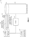
- FIG. 1 is a diagram to illustrate a particular embodiment of a system 100 of reducing power consumption of volatile memory by disabling the volatile memory, or a portion thereof, after processor-independent data transfer from the volatile memory to non-volatile memory.
- the system 100 may include a processor 102 that is coupled to a first volatile memory device 104 and the system 100 may include, or be coupled to, a non-volatile memory device 108.
- the system 100 of FIG. 1 may be included within an electronic device, such as a mobile phone, a tablet computing device, a laptop computing device, etc.
- the first volatile memory device 104 includes random access memory (RAM).
- the first volatile memory device 104 may be a dynamic random access memory (DRAM) device, such as a single-rank or dual-rank double data rate (DDR) synchronous DRAM device (also referred to herein as a "DDR").
- DRAM dynamic random access memory
- DDR dual-rank double data rate
- the first volatile memory device 104 may consume power (e.g., battery power) to refresh and maintain the data stored in the DRAM, even when the system 100 is in an inactive or sleep mode.
- power consumption of the first volatile memory device 104 may be reduced via techniques that involve disabling the first volatile memory device 104, or a portion thereof, after transferring data from the first volatile memory device 104 to the non-volatile memory device 108.
- the non-volatile memory device 108 may include a disk-based memory, a flash memory, a solid state memory, or some other type of non-volatile memory.
- the non-volatile memory device 108 may include NOR flash memory, NAND flash memory, an embedded MultiMediaCard (eMMC), or any combination thereof.
- eMMC embedded MultiMediaCard
- a portion 110 of the non-volatile memory device 108 may be reserved or allocated for data transfers from volatile memory in the system 100, such as from the first volatile memory device 104.
- less than the entire capacity of the non-volatile memory device 108 is available for general storage (e.g., storage of application/user data).
- the non-volatile memory device 108 may be substantially larger than the volatile memory device 104, reserving the portion 110 for data transfer may not have a noticeable impact on performance or user experience.
- a size of the reserved portion 110 is equal to a capacity of the first volatile memory device 104 or a fraction of the capacity of the first volatile memory device 104.
- the non-volatile memory device 108 may be a 16 gigabyte (GB) eMMC and the first volatile memory device 104 may be a 512 megabyte (MB) DDR.
- GB gigabyte
- MB 512 megabyte
- 512 MB or 256 MB, as an example, of the eMMC may be reserved for transfer of data from the DDR.
- the size of the reserved portion 110 may be equal to the capacity or a fraction of the capacity of one of the DDRs, a sum of the capacities or fractions of the capacities of more than one but not all of the DDRs, or a sum of the capacities or fractions of the capacities of all of the DDRs.
- data transfer between the first volatile memory device 104 and the non-volatile memory device 108 may be performed independent of the processor 102 (e.g., without sending the transferred data to the processor 102).
- a data transfer module 106 may be coupled to the first volatile memory device 104 and to the non-volatile memory device 108.
- the data transfer module 106 may include hardware such as a direct memory access (DMA) engine or controller, a direct data bus connection, etc. that is configured to copy data from the first volatile memory device 104 to the non-volatile memory device 108, and vice versa.
- DMA direct memory access
- the data transfer module 106 may transfer the entire contents of a 512 MB DDR (or a fraction of the contents of a 512 MB DDR) in less than a second while the processor 102 is power-collapsed (e.g., in sleep mode). Once the entire contents or a portion of the contents of the first volatile memory device 104 are copied to the non-volatile memory device 108, the first volatile memory device 104 or a portion of the first volatile memory device 104 may be disabled during sleep mode.
- disabling the first volatile memory device 104 or a portion of the first volatile memory device 104 may include turning off the first volatile memory device 104 or turning off the corresponding portion of the first volatile memory device 104, disabling refreshing of the first volatile memory device 104 or disabling refreshing of the corresponding portion of the first volatile memory device 104, or any combination thereof.
- the data transfer module 106 may be used to copy the data from the non-volatile memory device 108 back to the first volatile memory device 104.
- data is copied between the first volatile memory device 104 and the non-volatile memory device 108 in order by address.
- copying data "in order by address” means that each element of data that is copied from a volatile memory device is written back to the volatile memory device in the same location it was copied from prior to disabling the volatile memory device.
- a data image e.g., snapshot
- the entire first volatile memory device 104 e.g., a 512 MB data image
- active data e.g., data that is in use by a hardware component and/or software application at the system 100.
- Generating and copying a data image of the entire first volatile memory device 104 may be faster than compressing data or locating and copying only the active data to the non-volatile memory device 108. Moreover, because the size of the non-volatile memory device 108 may be significantly larger than the size of the first volatile memory device 104, the storage cost of copying a snapshot of the entire first volatile memory device 104 may be relatively small and acceptable to a user. In addition, because the data is transferred to and from the first volatile memory device 104 in order by address, memory mappings (e.g., virtual address to physical address mappings) in use prior to sleep mode may remain valid after exiting sleep mode. Further, unlike partial array self refresh (PASR) systems, data loss may be avoided when the first volatile memory device 104 is more than 50% full.
- PASR partial array self refresh
- a transition from a normal or active operating mode to a sleep mode may be initiated.
- the processor 102 or some other component (e.g., a power controller), may initiate the transition to sleep mode based on user input (e.g., a user depressing a power or standby button of an electronic device) or based on an event or interrupt (e.g., a timeout).
- the data transfer module 106 may copy data from the first volatile memory device 104 to the non-volatile memory device 108, as shown at 120.
- the processor 102 sends a message to the data transfer module 106 to trigger the copying.
- the first volatile memory device 104 may be disabled. For example, power to the first volatile memory device 104 may be turned off (e.g., by de-asserting an enable signal or power signal) and/or refreshing of the first volatile memory device 104 may be stopped (e.g., by de-asserting a refresh signal or setting a configuration value in a register or other memory associated with the first volatile memory device 104).
- the processor 102 or some other component (e.g., a power controller), may disable the first volatile memory device 104.
- the first volatile memory device 104 may consume less power in sleep mode as compared to existing systems that refresh DRAM devices during sleep mode.
- Other components of the system 100 may also be disabled during the sleep mode.
- the first volatile memory device 104 is enabled and the data stored in the non-volatile memory device 108 is copied back to the first volatile memory device 104 from the non-volatile memory device 108, as shown at 130.
- additional volatile memory devices may also be present in the system 100.
- a second volatile memory device 112 may be coupled to the processor 102.
- the volatile memory devices 104, 112 may be different ranks of a multi-rank DDR.
- the first volatile memory device 104 may be a 512 MB lower rank of a 1 GB DDR and the second volatile memory device 112 may be a 512 MB upper rank of the 1 GB DDR.
- Additional non-volatile memory devices and/or processors may also be present in the system 100.
- the number, configuration, capacity, and type of the various devices described herein should be considered merely illustrative, and not limiting.
- data from any number of the volatile memory devices (or ranks) may be transferred to the non-volatile memory device 108 in response to initiation of sleep mode.
- a mobile phone includes two DDRs (or a dual-rank DDR)
- one DDR (or rank) may be dedicated to multimedia applications/data and the other DDR (or rank) may be dedicated to modem applications/data and other "critical" data.
- data from the multimedia DDR (or rank) may be copied to non-volatile memory and the multimedia DDR (or rank) may be disabled during sleep mode to conserve power.
- modem applications/data may remain in the modem DDR (or rank), and the modem DDR (or rank) may continue to perform self-refreshes during sleep mode.
- Maintaining modem data and other critical data in the modem DDR (or rank) during the sleep mode may enable the mobile phone to more quickly respond to wireless cycles, such as paging cycles.
- certain application or user interface (UI) data such as a mobile phone unlock screen, may be maintained in the modem DDR (or rank) so that the mobile phone is responsive to user input when exiting the sleep mode, which may improve user experience.
- a multimedia memory and a non-critical portion (e.g., a lower rank) of a modem memory may be transferred to disk while a critical portion (e.g., an upper rank) of the modem memory may continue to be refreshed in sleep mode.
- the system 100 of FIG. 1 may support selective prioritization of certain data stored in volatile memory.
- application developers e.g., via an application programming interface (API), a compiler, a linker, etc.
- GUI graphical user interface
- application developers e.g., via an application programming interface (API), a compiler, a linker, etc.
- users e.g., via graphical user interface (GUI) options
- GUI graphical user interface
- the system 100 of FIG. 1 may thus reduce sleep floor current by copying data from volatile memory to non-volatile memory and disabling the volatile memory, or a portion thereof, during sleep mode, thereby avoiding power-consuming self-refresh operations on the volatile memory.
- the data transfer operation may be less computation and power intensive than page migrations associated with PASR.
- the data transfer operation may be performed using dedicated hardware (e.g., the data transfer module 106).
- the system 100 of FIG. 1 may enable dynamic memory management to balance power reduction with performance.
- less critical data from one DDR (or rank) may be copied to non-volatile memory so that the DDR (or rank) can be disabled during sleep mode, but more critical data may be maintained in another DDR (or rank) during the sleep mode to improve responsiveness and performance during/after sleep mode.
- FIG. 2 is a diagram to illustrate a particular embodiment of a system 200 of reducing power consumption of volatile memory by disabling the volatile memory, or a portion thereof, after processor-dependent data transfer from the volatile memory to non-volatile memory.
- the system 200 may include the processor 102, the first volatile memory device 104, and the non-volatile memory device 108 including the portion 110 reserved for data transfers from the first volatile memory device 104.
- FIG. 2 illustrates a data transfer module 206 within the processor 102.
- the data transfer module 206 may be implemented using hardware integrated into the processor 102 and/or instructions executable by the processor 102.
- the data transfer module 206 may be configured to transfer data between the first volatile memory device 104 and the non-volatile memory device 108 via the processor 102.
- the data transfer module 206 may perform processor-assisted (e.g., software-based) copying of a data image (e.g., snapshot) from the first volatile memory device 104 to the reserved portion 110 of the non-volatile memory device 108, as shown at 220.
- processor-assisted e.g., software-based
- the data transfer module 206 may perform processor-assisted (e.g., software-based) copying of the data image (e.g., snapshot) from the reserved portion of the non-volatile memory device 108 to the first volatile memory device 104, as shown at 230.
- FIG. 2 thus illustrates an alternative data transfer mechanism to that illustrated in FIG. 1 .
- the hardware-based processor-independent mechanism of FIG. 1 may perform data transfer faster
- the processor-assisted (e.g., software-based) mechanism of FIG. 2 may be implemented in existing electronic devices without introducing additional hardware elements that may increase a cost of manufacturing.
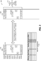
- FIG. 3 illustrates a particular embodiment of the data transfer operations of FIGs. 1-2 , and is generally designated 300.
- FIG. 3 illustrates a RAM 310 and a disk 320.
- the RAM 310 may be the first volatile memory device 104 of FIGs. 1-2 or the second volatile memory device 112 of FIG. 1 .
- the disk 320 may be the non-volatile memory device 108 of FIGs. 1-2 .
- data transfer between the RAM 310 and the disk 320 may be performed in order by address.
- memory mappings 330 may be in use and the RAM 310 may store six files (e.g., data files or code files), labeled A-F.
- Each of the files may include one or more portions (e.g., pages), as shown.
- the file A may include eight portions and the file B-F may each include two portions.
- the memory mappings 330 may indicate a starting address of each of the files.
- the starting address of the file A may be 0x0000 and the starting address of the file D may be 0x001F, as shown.
- a data image (e.g., snapshot) of the RAM 310 may be copied to a reserved portion 322 of the disk 320. As illustrated in FIG. 3 , each portion of each file may be copied to a corresponding location on the disk, and the relative ordering and placement of the portions of the files is maintained. In response to a transition out of the sleep mode, the data image may be copied back to the RAM 310. Thus, the memory mappings 330 that were in use prior to sleep mode may remain valid after exiting the sleep mode. For example, the eighth portion 312 of the file A may continue to be located at the address 0x0007, as shown.
- copying data in order by address e.g., without compression and/or relocation
- preserving memory mappings may simplify memory management and reduce preparation/clean-up operations associated with the systems of FIGs. 1-2 .
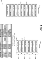
- FIG. 4 is a diagram to illustrate a particular aspect of a system 400 that is operable to reduce power consumption of volatile memory with respect to read-only data.
- FIGs. 1-3 illustrate techniques related to the invention to reduce sleep floor current while an electronic device is in sleep mode
- FIG. 4 illustrates a technique that may be applied during a "normal" (e.g., active) operating mode.
- the system 400 includes a volatile memory device (e.g., a synchronous DRAM (SDRAM) 402) and a non-volatile memory device (e.g., a NOR flash memory 404).
- the SDRAM 402 has four banks (banks 0-3). Power control for each bank may be independent, as further described herein.
- a copy of one or more segments of data stored in the NOR flash memory 404 may be loaded into the SDRAM 402.
- data associated with the application may be loaded into the SDRAM 402 for quicker access.
- data associated with an electronic device may be divided into two categories-read-only (“RO") data and read-write (“RW”) data.
- Read-only data is not modifiable (e.g., subject to read requests but not write requests), whereas read-write data is modifiable (e.g., subject to both read requests and write requests).
- Each application and subsystem (e.g., subsystem of an operating system) at the electronic device may include or be associated with read-only data and read-write data. For example, as shown in FIG.
- the NOR flash memory 404 may store read-only data and read-write data associated with Subsystem 0, Subsystem 1, Subsystem 2, Subsystem 3, and Subsystem 4.
- the NOR flash memory 404 may also store "critical" read-only data (e.g., read-only data for a modem in the case of a wireless phone).
- copies of various read-only and read-write data may be loaded in the SDRAM 402.
- a first copy 410 of the Subsystem 1 read-only data and a first copy 412 of the Subsystem 2 read-only data may be stored in the SDRAM 402.
- a second copy 420 of the Subsystem 1 read-only data and a second copy 422 of the Subsystem 2 read-only data may be stored in the NOR flash memory 404.
- a memory mapping for the data may identify the SDRAM 402.
- the memory mappings 440 e.g., a memory management unit (MMU) table
- "critical" read-only data 430 may be accessed from a physical address located in bank 3 of the SDRAM.
- MMU memory management unit
- the electronic device may monitor battery life. When the battery life falls below a threshold (e.g., 10%), the electronic device may enter a low performance mode (LPM). Alternately, or in addition, the LPM may be entered in response to a user command or user input requesting a transition to the LPM.
- the LPM may differ from sleep mode in that the LPM may provide continuous system operation, albeit at reduced performance.
- a memory mapping of read-only data may be updated from the SDRAM 402 to the NOR flash memory 404.
- mappings for the Subsystem 1 read-only data and the Subsystem 2 read-only data may be updated to point to physical addresses in the NOR flash memory 404 instead of bank 2 of the SDRAM 402.
- a portion of the SDRAM 402 that stores the read-only data may be disabled, and access requests (e.g., read requests) for the read-only data during the LPM may be directed to the NOR flash memory 404 instead of to the SDRAM 402.
- bank 2 of the SDRAM 402 may be disabled, and during the LPM access requests to read Subsystem 1 read-only data and Subsystem 2 read-only data may be directed to the NOR flash memory 404, in accordance with the updated memory mappings 440.
- disabling bank 2 of the SDRAM 402 during the LPM may include turning off bank 2 during the LPM (e.g., by de-asserting an enable signal or power signal) or disabling refreshing of bank 2 during the LPM (e.g., by de-asserting a refresh signal or setting a configuration value in a register). It will be appreciated that disabling a portion of the SDRAM 402 (or the entire SDRAM 402) during the LPM may reduce power consumption. Copies of read-write data and other read-only data (e.g., the "critical" read-only data 430) may continue to be accessed from the SDRAM 402 during the LPM.
- bank 2 of the SDRAM 402 may be enabled and the memory mappings 440 for the read-only data stored in bank 2 of the SDRAM 402 may be updated to point to bank 2 of the SDRAM 402 instead of to the NOR flash memory 404. Because the copy of the read-only data in the SDRAM 402 may have degraded during the LPM, a new copy of the read-only data may be loaded to the SDRAM 402 prior to updating the memory mappings 440.
- non-volatile memory in the system 400 may include NOR flash memory 404.
- the NOR flash memory 404 may enable execute-in-place (XIP) operation for executing stored code.
- XIP execute-in-place
- instructions corresponding to read-only code may be executed from the NOR flash memory 404 during the LPM without use of the SDRAM 402.
- additional operations may be performed (e.g., by an operating system or a controller) when transitioning into the LPM (e.g., prior to updating the memory mappings 440 to point to the NOR flash memory 404). For example, interrupts may be disabled, thread scheduling at a processor may be suspended, the processor may be switched from multi-threaded mode to single-threaded mode, and/or translation lookaside buffer (TLB) entries may be invalidated. Additional operations may also be performed (e.g., by an operating system or a controller) when transitioning out of the LPM (e.g., after updating the memory mappings 440 to point to the SDRAM 402). For example, interrupts may be enabled, thread scheduling may be resumed at the processor, and the processor may be switched from single-threaded mode to multi-threaded mode.
- TLB translation lookaside buffer
- subsystems e.g., a modem subsystem, a graphics subsystem, an audio subsystem, etc.
- subsystems may separate read-only data from read-write data.
- a linker used to create images corresponding to the subsystems may group read-only data separately from read-write data.
- certain read-only data may continue to reside in and be accessed from the SDRAM 402 during the LPM.
- the "critical" read-only data 430 may continue to be accessed from the SDRAM 402 during the LPM. Maintaining the "critical" read-only data 430 in an accessible state in the SDRAM 402 during the LPM may enable the system 400 to perform operations associated with the "critical" read-only data 430 in a shorter amount of time.
- the system 400 of FIG. 4 may be able to quickly respond to paging cycles while in the LPM.
- the system 400 of FIG. 4 may thus support selective prioritization of certain read-only data.
- GUI graphical user interface
- the system 400 of FIG. 4 may thus reduce power consumption in non-sleep (e.g., active) operating modes by accessing certain read-only data from non-volatile memory instead of volatile memory during low-power conditions. At least a portion of the volatile memory that stored the read-only data may be disabled, thereby avoiding power-consuming self-refresh operations on the portion of the volatile memory.
- non-sleep e.g., active
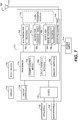
- FIG. 5 is a flowchart to illustrate a particular aspect of a method 500 of operation that may be performed at the systems of FIGs. 1-2 .
- the method 500 includes initiating a transition from an operating mode to a sleep mode at an electronic device, at 502.
- the electronic device may include a volatile memory device having a first size and a non-volatile memory device having a second size that is greater than or equal to the first size.
- the processor 102 may initiate a transition to sleep mode at an electronic device that includes the first volatile memory device 104 and the non-volatile memory device 108.
- the method 500 also includes, in response to the initiating, copying data from the volatile memory device to the non-volatile memory device, at 504.
- the data transfer module 106 may perform processor-independent copying of data from the first volatile memory device 104 to the non-volatile memory device 108.
- the data transfer module 206 may perform processor-assisted copying of data from the first volatile memory device 104 to the non-volatile memory device 108.
- the data may be copied in order by address, as described with reference to FIG. 3 .
- the method 500 further includes disabling the volatile memory device during the sleep mode, at 506.
- the processor 102 may disable the first volatile memory device 104.
- the method 500 also includes, in response to a transition from the sleep mode to the operating mode, enabling the volatile memory device and copying the data from the non-volatile memory device to the volatile memory device, at 508.
- the data transfer module 106 may perform processor-independent copying of the data from the non-volatile memory device 108 to the first volatile memory device 104.
- the data transfer module 206 may perform processor-assisted copying of the data from the non-volatile memory device 108 to the first volatile memory device 104.
- the method 500 of FIG. 5 may thus be used to reduce sleep floor current by copying data from volatile memory to non-volatile memory and disabling all or a portion of the volatile memory during sleep mode, thereby avoiding or reducing power-consuming self-refresh operations on the volatile memory, respectively.
- FIG. 6 is a flowchart to illustrate a particular aspect of a method 600 of operation that may be performed at the system of FIG. 4 .
- the method 600 includes operating an electronic device in normal mode, at 602.
- the electronic device may include a volatile memory device that stores a first copy of read-only data and a non-volatile memory device that stores a second copy of the read-only data.
- the SDRAM 402 stores the first copy 410 of the Subsystem 1 read-only data
- the NOR flash memory 404 stores the second copy 420 of the subsystem 1 read-only data.
- the method 600 also includes determining whether a LPM condition is satisfied, at 604. For example, the LPM condition may be satisfied in response to user input and/or when the remaining battery life of the electronic device is below a threshold (e.g., 10%). While the LPM condition is not satisfied, the method 600 returns to 602 and the electronic device continues operating in the normal mode while monitoring battery life.
- a threshold e.g. 10%
- the method 600 may optionally include disabling interrupts, suspending thread scheduling, switching from multi-threaded to single-threaded mode, and/or invalidating TLB entries, at 606.
- the method 600 also includes updating a memory mapping of read-only data from the volatile memory device to the non-volatile memory device, at 608.
- the mapping for the Subsystem 1 read-only data may be updated from 0x4000 (i.e., an address in bank 2 of the SDRAM 402) to 0xBBBB (i.e., an address in the NOR flash memory 404).
- the method 600 further includes disabling (e.g., turning off or disabling refreshing of) a portion of the volatile memory device that stores the first copy of the read-only data, at 610, and operating the electronic device in the LPM, at 612.
- Operating the electronic device in the LPM may include directing an access request for the read-only data to the non-volatile memory device instead of to the volatile memory device.
- the non-volatile memory device includes NOR flash memory and XIP execution of instructions may be performed from the NOR flash memory.
- the NOR flash memory may support XIP execution by providing a processor-like memory interface and addressing of individual words stored in the NOR flash memory.
- bank 2 of the SDRAM 402 may be disabled and the second copy 420 of the Subsystem 1 read-only data may be accessed during the LPM in accordance with the updated memory mappings 440.
- the method 600 includes determining whether the LPM condition continues to be satisfied, at 614. When the LPM condition is satisfied, the method 600 returns to 612 and the electronic device continues to operate in the LPM. When the LPM condition is no longer satisfied (e.g., battery life is greater than 10% or a user requests to exit the LPM), the method 600 includes enabling the portion of the volatile memory device, at 616, and copying the read-only data from the non-volatile memory device to the volatile memory device, at 618. For example, in FIG. 4 , bank 2 of the SDRAM 402 may be enabled and the Subsystem 1 read-only data may be copied to the SDRAM 402.
- the method 600 may optionally include enabling interrupts, resuming thread scheduling, and/or switching from single-threaded to multi-threaded mode, at 620.
- the method 600 further includes updating the memory mapping of the read-only data from the non-volatile memory device to the volatile memory device, at 622.
- the memory mapping of the Subsystem 1 read-only data may be updated from 0xBBBB back to 0x4000.
- the method 600 of FIG. 6 may thus be used to reduce power consumption by accessing read-only data from non-volatile memory instead of from volatile memory during low-power conditions. At least a portion of the volatile memory that stored the read-only data may be disabled, thereby avoiding power-consuming self-refresh operations on the portion of the volatile memory.
- an electronic device may implement all or a portion of either or both of the described techniques.
- a block diagram of an electronic device 700 including components operable to implement both techniques is shown.
- the electronic device 700, or components thereof may be included in a mobile phone, a set-top box, a music player, a video player, an entertainment unit, a navigation device, a communications device, a personal digital assistant (PDA), a fixed location data unit, a computing device, or any combination thereof.
- PDA personal digital assistant
- the electronic device 700 includes a processor 710 coupled to volatile memory device(s) and to non-volatile memory device(s).
- the volatile memory device(s) may include a multimedia DDR 762 (e.g., the first volatile memory device 104 of FIGs. 1-2 , the RAM 310 of FIG. 3 , and/or the SDRAM 402 of FIG. 4 ) and a modem DDR 764 (e.g., the second volatile memory device 112 of FIG. 1 , the RAM 310 of FIG. 3 , and/or the SDRAM 402 of FIG. 4 ).
- the non-volatile memory device(s) may include a NOR flash memory 766 (e.g., the non-volatile memory device 108 of FIGs.
- the multimedia DDR 762 may include a first copy 782 of read-only data and the NOR flash memory 766 may include a second copy 786 of the read-only data, as shown.
- the NOR flash memory 766 may also include a portion 784 that is reserved for data transfers from the multimedia DDR 762 and/or the modem DDR 764. Although two volatile memory devices and one non-volatile memory device are shown in FIG. 7 , it should be noted that other configurations having a different number of volatile and/or non-volatile memory device(s) may also be used.
- the processor 710 may include a power control module 792 and memory mappings 796 (e.g., the memory mappings 330 of FIG. 3 and/or the memory mappings 440 of FIG. 4 ).
- the processor 710 may include or implement a data transfer module 794 (e.g., the data transfer module 206 of FIG. 2 configured to perform processor-assisted data transfer).
- a data transfer module 770 e.g., the data transfer module 106 of FIG. 1 configured to perform processor-independent data transfer
- the electronic device 700 may perform various functions and methods described herein, such as the methods of FIGs. 5-6 .
- such functionality may be implemented using hardware.
- such functionality may be implemented using instructions that are stored in a tangible non-transitory medium (e.g., the multimedia DDR 762, the modem DDR 764, and/or the NOR flash memory 766) and that are executable by the processor 710.
- a tangible non-transitory medium e.g., the multimedia DDR 762, the modem DDR 764, and/or the NOR flash memory 766
- such functionality may be implemented using instructions 799, illustrated in FIG. 7 as being stored in the modem DDR 764.
- the power control module 792 may initiate a transition to sleep mode at the electronic device 700.
- the data transfer module 770 or the data transfer module 794 may copy data from the multimedia DDR 762 to the reserved portion 784 of the NOR flash memory 766. Data in the modem DDR 764 (e.g., "critical" data) may not be copied.
- the power control module 792 may disable the multimedia DDR 762 while leaving the modem DDR 764 enabled. Subsequently, the power control module 792 may initiate a transition out of the sleep mode.
- the data may be copied from the reserved portion 784 of the NOR flash memory 766 to the multimedia DDR 762.
- the data may be copied to and from the NOR flash memory 766 in order by address, so that the memory mappings 796 remain valid.
- the power control module 792 may detect a LPM condition.
- the memory mappings 796 may be updated such that access requests for certain read-only data during the LPM are directed to the second copy 786 stored in the NOR flash memory 766 instead of to the first copy 782 stored in the multimedia DDR 762.
- the multimedia DDR 762 may be disabled during the LPM.
- the power control module 792 detects that the LPM condition is no longer satisfied, the read-only data may be copied to the multimedia DDR 762 and the memory mappings 796 may be updated.
- FIG. 7 includes a display controller 726 that is coupled to the processor 710 and to a display 728.
- a coder/decoder (CODEC) 734 may be coupled to the processor 710.
- One or more speakers 736 and microphones 738 can be coupled to the CODEC 734.
- FIG. 7 also indicates that a wireless controller 740 can be coupled to the processor 710 and to an antenna 742 (e.g., via a radio frequency (RF) interface).
- RF radio frequency
- the processor 710, the display controller 726, the multimedia DDR 762, the modem DDR 764, the NOR flash memory 766, the CODEC 734, and the wireless controller 740 are included in a system-in-package or system-on-chip device 722.
- an input device 730 and a power supply 744 are coupled to the system-on-chip device 722.
- the display 728, the input device 730, the speaker(s) 736, the microphone(s) 738, the antenna 742, and the power supply 744 are external to the system-on-chip device 722.
- each of the display 728, the input device 730, the speaker 736, the microphone 738, the antenna 742, and the power supply 744 can be coupled to a component of the system-on-chip device 722, such as an interface or a controller.
- an apparatus may include a volatile memory device having a first size, a non-volatile memory device having a second size, and a processor.
- the processor may be configured to initiate a transition from an operating mode to a sleep mode and to disable the volatile memory device during the sleep mode.
- the apparatus may also include means for copying data from the volatile memory device to the non-volatile memory device in response to the initiating and prior to the disabling of the volatile memory device during the sleep mode.
- the means for copying may include the data transfer module 106 of FIG. 1 , the data transfer module 206 of FIG. 2 , the data transfer module 770 of FIG. 7 , the data transfer module 794 of FIG. 7 , one or more other devices or modules configured to copy data, or any combination thereof.
- Another apparatus may include a volatile memory device storing a first copy of read-only data and a non-volatile memory device storing a second copy of the read-only data.
- the apparatus may include means for updating, in response to a LPM condition being satisfied, a memory mapping of the read-only data from the volatile memory device to the non-volatile memory device.
- the means for updating may include the processor 102 of FIGs. 1-2 , the processor 710 of FIG. 7 , one or more other devices or modules (e.g., a memory controller, a memory management unit (MMU), etc.) configured to update memory mappings, or any combination thereof.
- MMU memory management unit
- the apparatus may further include means for disabling a portion of the volatile memory device that stores the first copy of the read-only data.
- the means for disabling may include the power control module 792 of FIG. 7 , one or more other devices or modules configured to disable a portion of a volatile memory device, or any combination thereof.
- the apparatus may include means for directing an access request for the read-only data to the non-volatile memory device instead of to the volatile memory device.
- the means for directing may include the processor 102 of FIGs. 1-2 , the processor 710 of FIG. 7 , one or more other devices or modules (e.g., a memory controller, a MMU, etc.) configured to direct memory accesses, or any combination thereof.
- the apparatus may also include means for determining that the LPM condition is satisfied.
- the means for determining may include the power control module 792 of FIG. 7 , one or more other devices or modules configured to determine whether a LPM condition is satisfied, or any combination thereof.
- a software module may reside in random access memory (RAM), flash memory, read-only memory (ROM), programmable read-only memory (PROM), erasable programmable read-only memory (EPROM), electrically erasable programmable read-only memory (EEPROM), registers, hard disk, a removable disk, a compact disc read-only memory (CD-ROM), or any other form of non-transient storage medium known in the art.
- An exemplary storage medium is coupled to the processor such that the processor can read information from, and write information to, the storage medium.
- the storage medium may be integral to the processor.
- the processor and the storage medium may reside in an application-specific integrated circuit (ASIC).
- ASIC application-specific integrated circuit
- the ASIC may reside in a computing device or a user terminal.
- the processor and the storage medium may reside as discrete components in a computing device or user terminal.
Landscapes
- Engineering & Computer Science (AREA)
- Theoretical Computer Science (AREA)
- Physics & Mathematics (AREA)
- General Engineering & Computer Science (AREA)
- General Physics & Mathematics (AREA)
- Memory System (AREA)
- Techniques For Improving Reliability Of Storages (AREA)
- Power Sources (AREA)
- Telephone Function (AREA)
Description
- The present disclosure is generally related to systems and methods of reducing power consumption of volatile memory via use of non-volatile memory.
- As portable computing devices such as mobile phones become smaller, the adverse effect of semiconductor leakage current on battery life may increase. For example, semiconductor leakage current may increase a sleep floor current of a mobile phone, where the sleep floor current represents a minimum amount of current that flows in the mobile phone while the mobile phone is in sleep mode and/or some other power-saving state such as idle mode, standby mode, etc. It is estimated that mobile phones may be in sleep mode over 95% of the time when the mobile phones are in idle standby mode. Thus, reducing the sleep floor current by even a small amount may result in a large increase in idle standby battery life.
- In mobile phones that utilize dynamic random access memory (DRAM), a large portion of the sleep floor current may be due to periodic refreshing of the DRAM. One way of reducing the contribution of memory refreshes to sleep floor current is to use partial array self refresh (PASR). In PASR, data in pages of an "upper" (or "lower") half of the DRAM is migrated to the pages of a "lower" (or "upper") half of the DRAM. After page migration is completed, the "lower" (or "upper") half of the memory may be refreshed during sleep mode but the "upper" (or "lower") half of the memory may not be refreshed, which may reduce an overall amount of memory refresh current being used. However, PASR may be inconvenient if more than 50% of the DRAM was originally being utilized. When more than 50% of the DRAM is being utilized, it may not be possible to consolidate all data into one half of the DRAM without compressing the data, which may be time consuming. The excess data may be deleted or may be left to deteriorate in the un-refreshed half of the DRAM during sleep mode.
- The page migration involved in PASR may also be time consuming and battery intensive (e.g., the page migration may take 10 to 40 seconds at 250 milliamps (mA)). Moreover, a reverse page migration may be performed when transitioning out of sleep mode depending on the memory allocation management in use (e.g., memory allocation management software of an operating system). Page migration may also be difficult to implement, because the location of empty pages in the DRAM may not be known until after the page migration has begun.
- Attention is drawn
US 2012/284475 A1 describing a memory controller for managing data and power in a memory. The memory controller is configured to identify a first area of the memory to be operated at a first power level, identify a second area of the memory to be operated at a second power level, transfer data in a region in the second area to a region in the first area, maintain a mapping of an address associated with the region in the second area to an address associated with the region in the first area, operate the first area at the first power level, and operate the second area at the second power level. - Attention is further drawn to
US 2011/231595 A1 describing systems and methods for storing hibernation data in a non-volatile memory ("NVM"). Hibernation data is data stored in volatile memory that is lost during a reduced power event, but is needed to restore the device to the operational state it was in prior to entering into the reduced power event. When a reduced power event occurs, the hibernation data is stored in the NVM. When the device "wakes up" the hibernation data is retrieved and used to restore the device to its prior operational state. - Further attention is drawn to
US 2012/102347 A1 describing a computing machine to power a memory to retain a process state of the computing machine if the computing machine is in a sleep state and transfer the process state from the memory to a non-volatile storage device, where the computing machine remains in the sleep state as the process state is transferred from the memory to the non-volatile storage device. - The present invention is set forth in the independent claims, respectively. Preferred embodiments of the invention are described in the dependent claims.
- Systems and methods of dynamic memory management to reduce power consumption are disclosed. The described techniques, or portions thereof, may be used during a sleep mode of an electronic device, during a normal operating mode of the electronic device, or any combination thereof.
- For example, a first technique may involve utilizing non-volatile memory at an electronic device to reduce sleep floor current. To illustrate, in addition to volatile memory (e.g., RAM), a mobile phone or other electronic device may include non-volatile memory, such as NOR Flash, NAND Flash, an embedded MultiMediaCard (eMMC), etc. A portion of the non-volatile memory may be reserved or allocated for data transfer from the volatile memory. When the mobile phone transitions into sleep mode, data from the volatile memory may be transferred, in order by address, to the reserved portion of the non-volatile memory. During sleep mode, the volatile memory may be turned off, which reduces the sleep floor current by avoiding DRAM self-refreshes. When exiting sleep mode, the data may be copied back to the volatile memory in order by address from the non-volatile memory. Because the data is transferred to and from the volatile memory in order by address, memory mappings in use prior to sleep mode remain valid after exiting sleep mode. The transfer mechanism between the volatile memory and the non-volatile memory may be processor-independent (e.g., using a direct memory access (DMA) engine, a direct bus connection, etc.) or may involve a processor (e.g., each data element may pass through the processor during copying).
- As another example, a second technique may involve monitoring battery life during normal (e.g., non-sleep) mode. When the battery life falls below a threshold, an electronic device may enter a low performance mode (LPM). The LPM may also be entered in response to a user command. The LPM may differ from sleep mode in that the LPM may provide continuous system operation, albeit at reduced performance. During the LPM, read-only data may be accessed from non-volatile memory instead of from the volatile memory. Upon entering the LPM, a memory mapping for the read-only data may be modified to point to a physical address in the non-volatile memory instead of a physical address in the volatile memory. To illustrate, the non-volatile memory may be a NOR Flash memory that enables execute-in-place (XIP) operation for executing stored code. During the LPM, self-refreshes of volatile memory portions that store the read-only data may be disabled, because the read-only data is being accessed from the non-volatile memory instead. Alternately, the volatile memory portions thereof may be turned off altogether during the LPM.
- In a particular aspect, a method includes initiating a transition from an operating mode to a sleep mode at an electronic device. The electronic device includes a volatile memory device having a first size and a non-volatile memory device having a second size that is greater than or equal to the first size. The method also includes, in response to the initiating, copying data from the volatile memory device to the non-volatile memory device. The method further includes disabling the volatile memory device during the sleep mode.
- In another particular aspect, an apparatus includes a volatile memory device having a first size and a non-volatile memory device having a second size that is greater than or equal to the first size. The apparatus also includes a processor configured to initiate a transition from an operating mode to a sleep mode and to disable the volatile memory device during the sleep mode. The apparatus further includes a data transfer module configured to copy data from the volatile memory device to the non-volatile memory device in response to the initiating and prior to the disabling of the volatile memory device during the sleep mode.
- In another particular aspect, a computer-readable storage device includes instructions that, when executed by a processor, cause the processor to initiate a transition from an operating mode to a sleep mode at an electronic device. The electronic device includes a volatile memory device having a first size and a non-volatile memory device having a second size that is greater than or equal to the first size. The instructions, when executed by the processor, also cause the processor to, in response to the initiating, cause copying of data from the volatile memory device to the non-volatile memory device. The instructions, when executed by the processor, further cause the processor to disable the volatile memory device during the sleep mode.
- In another particular aspect, an apparatus includes a volatile memory device having a first size and a non-volatile memory device having a second size that is greater than or equal to the first size. The apparatus also includes a processor configured to initiate a transition from an operating mode to a sleep mode and to disable the volatile memory device during the sleep mode. The apparatus further includes means for copying data from the volatile memory device to the non-volatile memory device in response to the initiating and prior to the disabling of the volatile memory device during the sleep mode.
- In another particular aspect, a method includes determining that a low performance mode (LPM) condition is satisfied at an electronic device. The electronic device includes a volatile memory device that stores a first copy of read-only data and a non-volatile memory device that stores a second copy of the read-only data. The method also includes, in response to the LPM condition being satisfied, updating a memory mapping of the read-only data from the volatile memory device to the non-volatile memory device. The method further includes disabling a portion of the volatile memory device that stores the first copy of the read-only data and directing an access request for the read-only data to the non-volatile memory device instead of to the volatile memory device.
- In another particular aspect, an apparatus includes a volatile memory device storing a first copy of read-only data and a non-volatile memory device storing a second copy of the read-only data. The apparatus also includes a processor configured to, in response to a LPM condition being satisfied, update a memory mapping of the read-only data from the volatile memory device to the non-volatile memory device. The processor is further configured to disable a portion of the volatile memory device that stores the first copy of the read-only data and to direct an access request for the read-only data to the non-volatile memory device instead of to the volatile memory device.
- In another particular aspect, a computer-readable storage device includes instructions that, when executed by a processor, cause the processor to, in response to a LPM condition being satisfied, update a memory mapping of read-only data from a volatile memory device to a non-volatile memory device. The LPM condition is satisfied at an electronic device that includes the volatile memory device storing a first copy of the read-only data and the non-volatile memory device storing a second copy of the read-only data. The instructions, when executed by the processor, further cause the processor to disable a portion of the volatile memory device that stores the first copy of the read-only data and to direct an access request for the read-only data to the non-volatile memory device instead of to the volatile memory device.
- In another particular aspect, an apparatus includes a volatile memory device storing a first copy of read-only data and a non-volatile memory device storing a second copy of the read-only data. The apparatus also includes means for updating, in response to a LPM condition being satisfied, a memory mapping of the read-only data from the volatile memory device to the non-volatile memory device. The apparatus further includes means for disabling a portion of the volatile memory device that stores the first copy of the read-only data and means for directing an access request for the read-only data to the non-volatile memory device instead of to the volatile memory device.
- One particular advantage provided by at least one of the disclosed aspects is an ability to decrease sleep floor current by disabling volatile memory, or a portion thereof; after copying data from the volatile memory to non-volatile memory in response to a transition to sleep mode. Another particular advantage is an ability to decrease memory refresh current by accessing read-only data from non-volatile memory instead of from volatile memory. Other aspects, advantages, and features of the present disclosure will become apparent after review of the entire application, including the following sections: Brief Description of the Drawings, Detailed Description, and the Claims.
-
-
FIG. 1 is a diagram to illustrate a particular embodiment of a system that is operable to reduce power consumption of volatile memory by disabling the volatile memory, or a portion thereof, after processor-independent data transfer from the volatile memory to non-volatile memory; -
FIG. 2 is a diagram to illustrate a particular embodiment of a system that is operable to reduce power consumption of volatile memory by disabling the volatile memory, or a portion thereof, after processor-dependent data transfer from the volatile memory to non-volatile memory; -
FIG. 3 is a diagram to illustrate a particular embodiment of the data transfer operations ofFIGs. 1-2 ; -
FIG. 4 is a diagram to illustrate a particular embodiment of a system that is operable to reduce power consumption of volatile memory with respect to read-only data; -
FIG. 5 is a flowchart to illustrate a particular embodiment of a method of operation at the systems ofFIGs. 1-2 ; -
FIG. 6 is a flowchart to illustrate a particular embodiment of a method of operation at the system ofFIG. 4 ; and -
FIG. 7 is a block diagram of a communication device including components operable to reduce power consumption of volatile memory via use of non-volatile memory. -
FIG. 1 is a diagram to illustrate a particular embodiment of asystem 100 of reducing power consumption of volatile memory by disabling the volatile memory, or a portion thereof, after processor-independent data transfer from the volatile memory to non-volatile memory. Thesystem 100 may include aprocessor 102 that is coupled to a firstvolatile memory device 104 and thesystem 100 may include, or be coupled to, anon-volatile memory device 108. In a particular embodiment, thesystem 100 ofFIG. 1 may be included within an electronic device, such as a mobile phone, a tablet computing device, a laptop computing device, etc. - In a particular embodiment, the first
volatile memory device 104 includes random access memory (RAM). For example, the firstvolatile memory device 104 may be a dynamic random access memory (DRAM) device, such as a single-rank or dual-rank double data rate (DDR) synchronous DRAM device (also referred to herein as a "DDR"). When the firstvolatile memory device 104 includes DRAM, the firstvolatile memory device 104 may consume power (e.g., battery power) to refresh and maintain the data stored in the DRAM, even when thesystem 100 is in an inactive or sleep mode. However, as further described herein, power consumption of the firstvolatile memory device 104 may be reduced via techniques that involve disabling the firstvolatile memory device 104, or a portion thereof, after transferring data from the firstvolatile memory device 104 to thenon-volatile memory device 108. - The
non-volatile memory device 108 may include a disk-based memory, a flash memory, a solid state memory, or some other type of non-volatile memory. For example, thenon-volatile memory device 108 may include NOR flash memory, NAND flash memory, an embedded MultiMediaCard (eMMC), or any combination thereof. In a particular embodiment, aportion 110 of thenon-volatile memory device 108 may be reserved or allocated for data transfers from volatile memory in thesystem 100, such as from the firstvolatile memory device 104. Thus, less than the entire capacity of thenon-volatile memory device 108 is available for general storage (e.g., storage of application/user data). However, because thenon-volatile memory device 108 may be substantially larger than thevolatile memory device 104, reserving theportion 110 for data transfer may not have a noticeable impact on performance or user experience. - In a particular aspect, a size of the reserved
portion 110 is equal to a capacity of the firstvolatile memory device 104 or a fraction of the capacity of the firstvolatile memory device 104. For example, thenon-volatile memory device 108 may be a 16 gigabyte (GB) eMMC and the firstvolatile memory device 104 may be a 512 megabyte (MB) DDR. Thus, 512 MB or 256 MB, as an example, of the eMMC may be reserved for transfer of data from the DDR. When multiple DDRs are present, the size of the reservedportion 110 may be equal to the capacity or a fraction of the capacity of one of the DDRs, a sum of the capacities or fractions of the capacities of more than one but not all of the DDRs, or a sum of the capacities or fractions of the capacities of all of the DDRs. - As shown in
FIG. 1 , data transfer between the firstvolatile memory device 104 and thenon-volatile memory device 108 may be performed independent of the processor 102 (e.g., without sending the transferred data to the processor 102). For example, adata transfer module 106 may be coupled to the firstvolatile memory device 104 and to thenon-volatile memory device 108. To illustrate, thedata transfer module 106 may include hardware such as a direct memory access (DMA) engine or controller, a direct data bus connection, etc. that is configured to copy data from the firstvolatile memory device 104 to thenon-volatile memory device 108, and vice versa. - In a particular embodiment, using the
data transfer module 106 to transfer data without sending the data to theprocessor 102 enables low-power high-speed transfer of the data. For example, thedata transfer module 106 may transfer the entire contents of a 512 MB DDR (or a fraction of the contents of a 512 MB DDR) in less than a second while theprocessor 102 is power-collapsed (e.g., in sleep mode). Once the entire contents or a portion of the contents of the firstvolatile memory device 104 are copied to thenon-volatile memory device 108, the firstvolatile memory device 104 or a portion of the firstvolatile memory device 104 may be disabled during sleep mode. For example, disabling the firstvolatile memory device 104 or a portion of the firstvolatile memory device 104 may include turning off the firstvolatile memory device 104 or turning off the corresponding portion of the firstvolatile memory device 104, disabling refreshing of the firstvolatile memory device 104 or disabling refreshing of the corresponding portion of the firstvolatile memory device 104, or any combination thereof. When thesystem 100 exits from sleep mode, thedata transfer module 106 may be used to copy the data from thenon-volatile memory device 108 back to the firstvolatile memory device 104. - In a particular aspect, data is copied between the first
volatile memory device 104 and thenon-volatile memory device 108 in order by address. As used herein, copying data "in order by address" means that each element of data that is copied from a volatile memory device is written back to the volatile memory device in the same location it was copied from prior to disabling the volatile memory device. For example, a data image (e.g., snapshot) of the entire first volatile memory device 104 (e.g., a 512 MB data image) may be copied to thenon-volatile memory device 108, regardless of whether or not the entire DDR firstvolatile memory device 104 was storing active data (e.g., data that is in use by a hardware component and/or software application at the system 100). Generating and copying a data image of the entire firstvolatile memory device 104 may be faster than compressing data or locating and copying only the active data to thenon-volatile memory device 108. Moreover, because the size of thenon-volatile memory device 108 may be significantly larger than the size of the firstvolatile memory device 104, the storage cost of copying a snapshot of the entire firstvolatile memory device 104 may be relatively small and acceptable to a user. In addition, because the data is transferred to and from the firstvolatile memory device 104 in order by address, memory mappings (e.g., virtual address to physical address mappings) in use prior to sleep mode may remain valid after exiting sleep mode. Further, unlike partial array self refresh (PASR) systems, data loss may be avoided when the firstvolatile memory device 104 is more than 50% full. - During operation, a transition from a normal or active operating mode to a sleep mode may be initiated. For example, the
processor 102, or some other component (e.g., a power controller), may initiate the transition to sleep mode based on user input (e.g., a user depressing a power or standby button of an electronic device) or based on an event or interrupt (e.g., a timeout). In response to the initiation of the transition to the sleep mode, thedata transfer module 106 may copy data from the firstvolatile memory device 104 to thenon-volatile memory device 108, as shown at 120. In a particular embodiment, theprocessor 102 sends a message to thedata transfer module 106 to trigger the copying. - After the data has been copied, the first
volatile memory device 104 may be disabled. For example, power to the firstvolatile memory device 104 may be turned off (e.g., by de-asserting an enable signal or power signal) and/or refreshing of the firstvolatile memory device 104 may be stopped (e.g., by de-asserting a refresh signal or setting a configuration value in a register or other memory associated with the first volatile memory device 104). In a particular embodiment, theprocessor 102, or some other component (e.g., a power controller), may disable the firstvolatile memory device 104. Thus, the firstvolatile memory device 104 may consume less power in sleep mode as compared to existing systems that refresh DRAM devices during sleep mode. Other components of thesystem 100, such as theprocessor 102 and/or thenon-volatile memory device 108, may also be disabled during the sleep mode. In response to a transition from the sleep mode back to the normal or active operating mode, the firstvolatile memory device 104 is enabled and the data stored in thenon-volatile memory device 108 is copied back to the firstvolatile memory device 104 from thenon-volatile memory device 108, as shown at 130. - In a particular aspect, additional volatile memory devices may also be present in the
system 100. For example, a secondvolatile memory device 112 may be coupled to theprocessor 102. Alternately, thevolatile memory devices volatile memory device 104 may be a 512 MB lower rank of a 1 GB DDR and the secondvolatile memory device 112 may be a 512 MB upper rank of the 1 GB DDR. Additional non-volatile memory devices and/or processors may also be present in thesystem 100. Thus, the number, configuration, capacity, and type of the various devices described herein should be considered merely illustrative, and not limiting. When multiple volatile memory devices are present (or a multi-rank volatile memory device is present), data from any number of the volatile memory devices (or ranks) may be transferred to thenon-volatile memory device 108 in response to initiation of sleep mode. - For example, if a mobile phone includes two DDRs (or a dual-rank DDR), one DDR (or rank) may be dedicated to multimedia applications/data and the other DDR (or rank) may be dedicated to modem applications/data and other "critical" data. In that case, data from the multimedia DDR (or rank) may be copied to non-volatile memory and the multimedia DDR (or rank) may be disabled during sleep mode to conserve power. However, modem applications/data may remain in the modem DDR (or rank), and the modem DDR (or rank) may continue to perform self-refreshes during sleep mode. Maintaining modem data and other critical data in the modem DDR (or rank) during the sleep mode may enable the mobile phone to more quickly respond to wireless cycles, such as paging cycles. In some aspects, certain application or user interface (UI) data, such as a mobile phone unlock screen, may be maintained in the modem DDR (or rank) so that the mobile phone is responsive to user input when exiting the sleep mode, which may improve user experience.
- It will be appreciated that other memory configurations may benefit from the
system 100 ofFIG. 1 . For example, the entire contents of a multimedia memory and a non-critical portion (e.g., a lower rank) of a modem memory may be transferred to disk while a critical portion (e.g., an upper rank) of the modem memory may continue to be refreshed in sleep mode. - In a particular embodiment, the
system 100 ofFIG. 1 may support selective prioritization of certain data stored in volatile memory. For example, application developers (e.g., via an application programming interface (API), a compiler, a linker, etc.) or users (e.g., via graphical user interface (GUI) options) may be able to specify whether an allocation of dynamic memory (e.g., requested by an application or an operating system) or loading of data (e.g., requested by an application or an operating system) should take place in higher-priority volatile memory that will remain enabled during sleep mode or in lower-priority volatile memory that will be disabled during sleep mode after data is transferred to a non-volatile memory. - The
system 100 ofFIG. 1 may thus reduce sleep floor current by copying data from volatile memory to non-volatile memory and disabling the volatile memory, or a portion thereof, during sleep mode, thereby avoiding power-consuming self-refresh operations on the volatile memory. Advantageously, the data transfer operation may be less computation and power intensive than page migrations associated with PASR. For example, the data transfer operation may be performed using dedicated hardware (e.g., the data transfer module 106). Further, thesystem 100 ofFIG. 1 may enable dynamic memory management to balance power reduction with performance. For example, less critical data from one DDR (or rank) may be copied to non-volatile memory so that the DDR (or rank) can be disabled during sleep mode, but more critical data may be maintained in another DDR (or rank) during the sleep mode to improve responsiveness and performance during/after sleep mode. -
FIG. 2 is a diagram to illustrate a particular embodiment of asystem 200 of reducing power consumption of volatile memory by disabling the volatile memory, or a portion thereof, after processor-dependent data transfer from the volatile memory to non-volatile memory. Thesystem 200 may include theprocessor 102, the firstvolatile memory device 104, and thenon-volatile memory device 108 including theportion 110 reserved for data transfers from the firstvolatile memory device 104. -
FIG. 2 illustrates adata transfer module 206 within theprocessor 102. For example, thedata transfer module 206 may be implemented using hardware integrated into theprocessor 102 and/or instructions executable by theprocessor 102. Thedata transfer module 206 may be configured to transfer data between the firstvolatile memory device 104 and thenon-volatile memory device 108 via theprocessor 102. - For example, in response to initiation of a transition to sleep mode, the
data transfer module 206 may perform processor-assisted (e.g., software-based) copying of a data image (e.g., snapshot) from the firstvolatile memory device 104 to the reservedportion 110 of thenon-volatile memory device 108, as shown at 220. As another example, in response to a transition out of the sleep mode, thedata transfer module 206 may perform processor-assisted (e.g., software-based) copying of the data image (e.g., snapshot) from the reserved portion of thenon-volatile memory device 108 to the firstvolatile memory device 104, as shown at 230. -
FIG. 2 thus illustrates an alternative data transfer mechanism to that illustrated inFIG. 1 . Whereas the hardware-based processor-independent mechanism ofFIG. 1 may perform data transfer faster, the processor-assisted (e.g., software-based) mechanism ofFIG. 2 may be implemented in existing electronic devices without introducing additional hardware elements that may increase a cost of manufacturing. -
FIG. 3 illustrates a particular embodiment of the data transfer operations ofFIGs. 1-2 , and is generally designated 300.FIG. 3 illustrates aRAM 310 and adisk 320. For example, theRAM 310 may be the firstvolatile memory device 104 ofFIGs. 1-2 or the secondvolatile memory device 112 ofFIG. 1 . Thedisk 320 may be thenon-volatile memory device 108 ofFIGs. 1-2 . - As described with reference to
FIGs. 1-2 , data transfer between theRAM 310 and thedisk 320 may be performed in order by address. Prior to the data transfer,memory mappings 330 may be in use and theRAM 310 may store six files (e.g., data files or code files), labeled A-F. Each of the files may include one or more portions (e.g., pages), as shown. For example, the file A may include eight portions and the file B-F may each include two portions. Thememory mappings 330 may indicate a starting address of each of the files. For example, the starting address of the file A may be 0x0000 and the starting address of the file D may be 0x001F, as shown. - In response to initiation of a transition to sleep mode, a data image (e.g., snapshot) of the
RAM 310 may be copied to areserved portion 322 of thedisk 320. As illustrated inFIG. 3 , each portion of each file may be copied to a corresponding location on the disk, and the relative ordering and placement of the portions of the files is maintained. In response to a transition out of the sleep mode, the data image may be copied back to theRAM 310. Thus, thememory mappings 330 that were in use prior to sleep mode may remain valid after exiting the sleep mode. For example, theeighth portion 312 of the file A may continue to be located at the address 0x0007, as shown. - It will be appreciated that copying data in order by address (e.g., without compression and/or relocation) and preserving memory mappings, as shown in
FIG. 3 , may simplify memory management and reduce preparation/clean-up operations associated with the systems ofFIGs. 1-2 . -
FIG. 4 is a diagram to illustrate a particular aspect of asystem 400 that is operable to reduce power consumption of volatile memory with respect to read-only data. WhereasFIGs. 1-3 illustrate techniques related to the invention to reduce sleep floor current while an electronic device is in sleep mode,FIG. 4 illustrates a technique that may be applied during a "normal" (e.g., active) operating mode. Thesystem 400 includes a volatile memory device (e.g., a synchronous DRAM (SDRAM) 402) and a non-volatile memory device (e.g., a NOR flash memory 404). In the aspect ofFIG. 4 , theSDRAM 402 has four banks (banks 0-3). Power control for each bank may be independent, as further described herein. - During operation, a copy of one or more segments of data stored in the NOR
flash memory 404 may be loaded into theSDRAM 402. For example, when a particular application is executing, data associated with the application may be loaded into theSDRAM 402 for quicker access. Generally, data associated with an electronic device may be divided into two categories-read-only ("RO") data and read-write ("RW") data. Read-only data is not modifiable (e.g., subject to read requests but not write requests), whereas read-write data is modifiable (e.g., subject to both read requests and write requests). Each application and subsystem (e.g., subsystem of an operating system) at the electronic device may include or be associated with read-only data and read-write data. For example, as shown inFIG. 4 , the NORflash memory 404 may store read-only data and read-write data associated withSubsystem 0,Subsystem 1,Subsystem 2,Subsystem 3, andSubsystem 4. The NORflash memory 404 may also store "critical" read-only data (e.g., read-only data for a modem in the case of a wireless phone). - As shown in
FIG. 4 , copies of various read-only and read-write data may be loaded in theSDRAM 402. For example, afirst copy 410 of theSubsystem 1 read-only data and afirst copy 412 of theSubsystem 2 read-only data may be stored in theSDRAM 402. Asecond copy 420 of theSubsystem 1 read-only data and asecond copy 422 of theSubsystem 2 read-only data may be stored in the NORflash memory 404. When data is being accessed from theSDRAM 402, a memory mapping for the data may identify theSDRAM 402. For example, as shown in the memory mappings 440 (e.g., a memory management unit (MMU) table), "critical" read-only data 430 may be accessed from a physical address located inbank 3 of the SDRAM. - During operation, the electronic device may monitor battery life. When the battery life falls below a threshold (e.g., 10%), the electronic device may enter a low performance mode (LPM). Alternately, or in addition, the LPM may be entered in response to a user command or user input requesting a transition to the LPM. The LPM may differ from sleep mode in that the LPM may provide continuous system operation, albeit at reduced performance.
- In response to an LPM condition (e.g., battery life being less than or equal to 10%) being satisfied, a memory mapping of read-only data may be updated from the
SDRAM 402 to the NORflash memory 404. For example, as shown in thememory mappings 440, mappings for theSubsystem 1 read-only data and theSubsystem 2 read-only data may be updated to point to physical addresses in the NORflash memory 404 instead ofbank 2 of theSDRAM 402. A portion of theSDRAM 402 that stores the read-only data may be disabled, and access requests (e.g., read requests) for the read-only data during the LPM may be directed to the NORflash memory 404 instead of to theSDRAM 402. For example,bank 2 of theSDRAM 402 may be disabled, and during the LPM access requests to readSubsystem 1 read-only data andSubsystem 2 read-only data may be directed to the NORflash memory 404, in accordance with the updatedmemory mappings 440. - In a particular aspect, disabling
bank 2 of theSDRAM 402 during the LPM may include turning offbank 2 during the LPM (e.g., by de-asserting an enable signal or power signal) or disabling refreshing ofbank 2 during the LPM (e.g., by de-asserting a refresh signal or setting a configuration value in a register). It will be appreciated that disabling a portion of the SDRAM 402 (or the entire SDRAM 402) during the LPM may reduce power consumption. Copies of read-write data and other read-only data (e.g., the "critical" read-only data 430) may continue to be accessed from theSDRAM 402 during the LPM. - In response to a determination that the LPM condition is no longer satisfied (e.g., battery life exceeds 10%),
bank 2 of theSDRAM 402 may be enabled and thememory mappings 440 for the read-only data stored inbank 2 of theSDRAM 402 may be updated to point tobank 2 of theSDRAM 402 instead of to the NORflash memory 404. Because the copy of the read-only data in theSDRAM 402 may have degraded during the LPM, a new copy of the read-only data may be loaded to theSDRAM 402 prior to updating thememory mappings 440. - In a particular aspect, as shown in
FIG. 4 , non-volatile memory in thesystem 400 may include NORflash memory 404. The NORflash memory 404 may enable execute-in-place (XIP) operation for executing stored code. Thus, instructions corresponding to read-only code may be executed from the NORflash memory 404 during the LPM without use of theSDRAM 402. - In a particular aspect, additional operations may be performed (e.g., by an operating system or a controller) when transitioning into the LPM (e.g., prior to updating the
memory mappings 440 to point to the NOR flash memory 404). For example, interrupts may be disabled, thread scheduling at a processor may be suspended, the processor may be switched from multi-threaded mode to single-threaded mode, and/or translation lookaside buffer (TLB) entries may be invalidated. Additional operations may also be performed (e.g., by an operating system or a controller) when transitioning out of the LPM (e.g., after updating thememory mappings 440 to point to the SDRAM 402). For example, interrupts may be enabled, thread scheduling may be resumed at the processor, and the processor may be switched from single-threaded mode to multi-threaded mode. - In a particular aspect, to support implementation of the LPM, subsystems (e.g., a modem subsystem, a graphics subsystem, an audio subsystem, etc.) of an electronic device may separate read-only data from read-write data. For example, a linker used to create images corresponding to the subsystems may group read-only data separately from read-write data.
- In a particular aspect, certain read-only data may continue to reside in and be accessed from the
SDRAM 402 during the LPM. For example, the "critical" read-only data 430 may continue to be accessed from theSDRAM 402 during the LPM. Maintaining the "critical" read-only data 430 in an accessible state in theSDRAM 402 during the LPM may enable thesystem 400 to perform operations associated with the "critical" read-only data 430 in a shorter amount of time. For example, when the "critical" read-only data 430 includes modem data, thesystem 400 ofFIG. 4 may be able to quickly respond to paging cycles while in the LPM. Thesystem 400 ofFIG. 4 may thus support selective prioritization of certain read-only data. For example, application developers (e.g., via an application programming interface (API), a compiler, a linker, etc.) or users (e.g., via graphical user interface (GUI) options) may be able to specify whether particular read-only data should continue to be accessed from volatile memory (e.g., the SDRAM 402) during the LPM. - The
system 400 ofFIG. 4 may thus reduce power consumption in non-sleep (e.g., active) operating modes by accessing certain read-only data from non-volatile memory instead of volatile memory during low-power conditions. At least a portion of the volatile memory that stored the read-only data may be disabled, thereby avoiding power-consuming self-refresh operations on the portion of the volatile memory. -
FIG. 5 is a flowchart to illustrate a particular aspect of amethod 500 of operation that may be performed at the systems ofFIGs. 1-2 . - The
method 500 includes initiating a transition from an operating mode to a sleep mode at an electronic device, at 502. The electronic device may include a volatile memory device having a first size and a non-volatile memory device having a second size that is greater than or equal to the first size. For example, referring toFIG. 1 orFIG. 2 , theprocessor 102 may initiate a transition to sleep mode at an electronic device that includes the firstvolatile memory device 104 and thenon-volatile memory device 108. - The
method 500 also includes, in response to the initiating, copying data from the volatile memory device to the non-volatile memory device, at 504. For example, referring toFIG. 1 , thedata transfer module 106 may perform processor-independent copying of data from the firstvolatile memory device 104 to thenon-volatile memory device 108. As another example, referring toFIG. 2 , thedata transfer module 206 may perform processor-assisted copying of data from the firstvolatile memory device 104 to thenon-volatile memory device 108. In a particular embodiment, the data may be copied in order by address, as described with reference toFIG. 3 . - The
method 500 further includes disabling the volatile memory device during the sleep mode, at 506. For example, referring toFIG. 1 orFIG. 2 , theprocessor 102 may disable the firstvolatile memory device 104. Themethod 500 also includes, in response to a transition from the sleep mode to the operating mode, enabling the volatile memory device and copying the data from the non-volatile memory device to the volatile memory device, at 508. For example, referring toFIG. 1 , thedata transfer module 106 may perform processor-independent copying of the data from thenon-volatile memory device 108 to the firstvolatile memory device 104. As another example, referring toFIG. 2 , thedata transfer module 206 may perform processor-assisted copying of the data from thenon-volatile memory device 108 to the firstvolatile memory device 104. - The
method 500 ofFIG. 5 may thus be used to reduce sleep floor current by copying data from volatile memory to non-volatile memory and disabling all or a portion of the volatile memory during sleep mode, thereby avoiding or reducing power-consuming self-refresh operations on the volatile memory, respectively. -
FIG. 6 is a flowchart to illustrate a particular aspect of amethod 600 of operation that may be performed at the system ofFIG. 4 . - The
method 600 includes operating an electronic device in normal mode, at 602. The electronic device may include a volatile memory device that stores a first copy of read-only data and a non-volatile memory device that stores a second copy of the read-only data. For example, inFIG. 4 , theSDRAM 402 stores thefirst copy 410 of theSubsystem 1 read-only data and the NORflash memory 404 stores thesecond copy 420 of thesubsystem 1 read-only data. - The
method 600 also includes determining whether a LPM condition is satisfied, at 604. For example, the LPM condition may be satisfied in response to user input and/or when the remaining battery life of the electronic device is below a threshold (e.g., 10%). While the LPM condition is not satisfied, themethod 600 returns to 602 and the electronic device continues operating in the normal mode while monitoring battery life. - When the LPM condition is satisfied, the
method 600 may optionally include disabling interrupts, suspending thread scheduling, switching from multi-threaded to single-threaded mode, and/or invalidating TLB entries, at 606. Themethod 600 also includes updating a memory mapping of read-only data from the volatile memory device to the non-volatile memory device, at 608. For example, in thememory mappings 440 ofFIG. 4 , the mapping for theSubsystem 1 read-only data may be updated from 0x4000 (i.e., an address inbank 2 of the SDRAM 402) to 0xBBBB (i.e., an address in the NOR flash memory 404). - The
method 600 further includes disabling (e.g., turning off or disabling refreshing of) a portion of the volatile memory device that stores the first copy of the read-only data, at 610, and operating the electronic device in the LPM, at 612. Operating the electronic device in the LPM may include directing an access request for the read-only data to the non-volatile memory device instead of to the volatile memory device. In a particular embodiment, the non-volatile memory device includes NOR flash memory and XIP execution of instructions may be performed from the NOR flash memory. To illustrate, the NOR flash memory may support XIP execution by providing a processor-like memory interface and addressing of individual words stored in the NOR flash memory. For example, referring toFIG. 4 ,bank 2 of theSDRAM 402 may be disabled and thesecond copy 420 of theSubsystem 1 read-only data may be accessed during the LPM in accordance with the updatedmemory mappings 440. - During the LPM, the
method 600 includes determining whether the LPM condition continues to be satisfied, at 614. When the LPM condition is satisfied, themethod 600 returns to 612 and the electronic device continues to operate in the LPM. When the LPM condition is no longer satisfied (e.g., battery life is greater than 10% or a user requests to exit the LPM), themethod 600 includes enabling the portion of the volatile memory device, at 616, and copying the read-only data from the non-volatile memory device to the volatile memory device, at 618. For example, inFIG. 4 ,bank 2 of theSDRAM 402 may be enabled and theSubsystem 1 read-only data may be copied to theSDRAM 402. - The
method 600 may optionally include enabling interrupts, resuming thread scheduling, and/or switching from single-threaded to multi-threaded mode, at 620. Themethod 600 further includes updating the memory mapping of the read-only data from the non-volatile memory device to the volatile memory device, at 622. For example, inFIG. 4 , the memory mapping of theSubsystem 1 read-only data may be updated from 0xBBBB back to 0x4000. - The
method 600 ofFIG. 6 may thus be used to reduce power consumption by accessing read-only data from non-volatile memory instead of from volatile memory during low-power conditions. At least a portion of the volatile memory that stored the read-only data may be disabled, thereby avoiding power-consuming self-refresh operations on the portion of the volatile memory. - It should be noted that although
FIGs. 1-3 and5 describe a sleep mode technique andFIGs. 4 and6 describe a normal mode technique, this organization is for ease of explanation only. In accordance with the disclosure, an electronic device (e.g., a mobile phone) may implement all or a portion of either or both of the described techniques. For example, referring toFIG. 7 , a block diagram of anelectronic device 700 including components operable to implement both techniques is shown. In a particular embodiment, theelectronic device 700, or components thereof, may be included in a mobile phone, a set-top box, a music player, a video player, an entertainment unit, a navigation device, a communications device, a personal digital assistant (PDA), a fixed location data unit, a computing device, or any combination thereof. - The
electronic device 700 includes aprocessor 710 coupled to volatile memory device(s) and to non-volatile memory device(s). For example, the volatile memory device(s) may include a multimedia DDR 762 (e.g., the firstvolatile memory device 104 ofFIGs. 1-2 , theRAM 310 ofFIG. 3 , and/or theSDRAM 402 ofFIG. 4 ) and a modem DDR 764 (e.g., the secondvolatile memory device 112 ofFIG. 1 , theRAM 310 ofFIG. 3 , and/or theSDRAM 402 ofFIG. 4 ). The non-volatile memory device(s) may include a NOR flash memory 766 (e.g., thenon-volatile memory device 108 of FIGs. 102, thedisk 320 ofFIG. 3 , and/or the NORflash memory 404 ofFIG. 4 ). Themultimedia DDR 762 may include afirst copy 782 of read-only data and the NORflash memory 766 may include asecond copy 786 of the read-only data, as shown. The NORflash memory 766 may also include aportion 784 that is reserved for data transfers from themultimedia DDR 762 and/or themodem DDR 764. Although two volatile memory devices and one non-volatile memory device are shown inFIG. 7 , it should be noted that other configurations having a different number of volatile and/or non-volatile memory device(s) may also be used. - The
processor 710 may include apower control module 792 and memory mappings 796 (e.g., thememory mappings 330 ofFIG. 3 and/or thememory mappings 440 ofFIG. 4 ). In a particular embodiment, theprocessor 710 may include or implement a data transfer module 794 (e.g., thedata transfer module 206 ofFIG. 2 configured to perform processor-assisted data transfer). Alternately, or in addition, a data transfer module 770 (e.g., thedata transfer module 106 ofFIG. 1 configured to perform processor-independent data transfer) may be coupled to themultimedia DDR 762, themodem DDR 764, and/or the NORflash memory 766, as shown. - During operation, the
electronic device 700 may perform various functions and methods described herein, such as the methods ofFIGs. 5-6 . In a particular embodiment, such functionality may be implemented using hardware. Alternately, or in addition, such functionality may be implemented using instructions that are stored in a tangible non-transitory medium (e.g., themultimedia DDR 762, themodem DDR 764, and/or the NOR flash memory 766) and that are executable by theprocessor 710. For example, such functionality may be implemented usinginstructions 799, illustrated inFIG. 7 as being stored in themodem DDR 764. - For example, the
power control module 792 may initiate a transition to sleep mode at theelectronic device 700. In response to initiating the sleep mode, thedata transfer module 770 or thedata transfer module 794 may copy data from themultimedia DDR 762 to the reservedportion 784 of the NORflash memory 766. Data in the modem DDR 764 (e.g., "critical" data) may not be copied. Thepower control module 792 may disable themultimedia DDR 762 while leaving themodem DDR 764 enabled. Subsequently, thepower control module 792 may initiate a transition out of the sleep mode. The data may be copied from the reservedportion 784 of the NORflash memory 766 to themultimedia DDR 762. The data may be copied to and from the NORflash memory 766 in order by address, so that thememory mappings 796 remain valid. - As another example, the
power control module 792 may detect a LPM condition. In response, thememory mappings 796 may be updated such that access requests for certain read-only data during the LPM are directed to thesecond copy 786 stored in the NORflash memory 766 instead of to thefirst copy 782 stored in themultimedia DDR 762. Themultimedia DDR 762 may be disabled during the LPM. When thepower control module 792 detects that the LPM condition is no longer satisfied, the read-only data may be copied to themultimedia DDR 762 and thememory mappings 796 may be updated. -
FIG. 7 includes adisplay controller 726 that is coupled to theprocessor 710 and to adisplay 728. A coder/decoder (CODEC) 734 may be coupled to theprocessor 710. One ormore speakers 736 andmicrophones 738 can be coupled to theCODEC 734.FIG. 7 also indicates that awireless controller 740 can be coupled to theprocessor 710 and to an antenna 742 (e.g., via a radio frequency (RF) interface). - In a particular embodiment, the
processor 710, thedisplay controller 726, themultimedia DDR 762, themodem DDR 764, the NORflash memory 766, theCODEC 734, and thewireless controller 740 are included in a system-in-package or system-on-chip device 722. In a particular embodiment, aninput device 730 and apower supply 744 are coupled to the system-on-chip device 722. Moreover, in a particular embodiment, as illustrated inFIG. 7 , thedisplay 728, theinput device 730, the speaker(s) 736, the microphone(s) 738, theantenna 742, and thepower supply 744 are external to the system-on-chip device 722. However, each of thedisplay 728, theinput device 730, thespeaker 736, themicrophone 738, theantenna 742, and thepower supply 744 can be coupled to a component of the system-on-chip device 722, such as an interface or a controller. - In conjunction with the described aspects, an apparatus may include a volatile memory device having a first size, a non-volatile memory device having a second size, and a processor. The processor may be configured to initiate a transition from an operating mode to a sleep mode and to disable the volatile memory device during the sleep mode. The apparatus may also include means for copying data from the volatile memory device to the non-volatile memory device in response to the initiating and prior to the disabling of the volatile memory device during the sleep mode. For example, the means for copying may include the
data transfer module 106 ofFIG. 1 , thedata transfer module 206 ofFIG. 2 , thedata transfer module 770 ofFIG. 7 , thedata transfer module 794 ofFIG. 7 , one or more other devices or modules configured to copy data, or any combination thereof. - Another apparatus may include a volatile memory device storing a first copy of read-only data and a non-volatile memory device storing a second copy of the read-only data. The apparatus may include means for updating, in response to a LPM condition being satisfied, a memory mapping of the read-only data from the volatile memory device to the non-volatile memory device. For example, the means for updating may include the
processor 102 ofFIGs. 1-2 , theprocessor 710 ofFIG. 7 , one or more other devices or modules (e.g., a memory controller, a memory management unit (MMU), etc.) configured to update memory mappings, or any combination thereof. - The apparatus may further include means for disabling a portion of the volatile memory device that stores the first copy of the read-only data. For example, the means for disabling may include the
power control module 792 ofFIG. 7 , one or more other devices or modules configured to disable a portion of a volatile memory device, or any combination thereof. - The apparatus may include means for directing an access request for the read-only data to the non-volatile memory device instead of to the volatile memory device. For example, the means for directing may include the
processor 102 ofFIGs. 1-2 , theprocessor 710 ofFIG. 7 , one or more other devices or modules (e.g., a memory controller, a MMU, etc.) configured to direct memory accesses, or any combination thereof. - The apparatus may also include means for determining that the LPM condition is satisfied. For example, the means for determining may include the
power control module 792 ofFIG. 7 , one or more other devices or modules configured to determine whether a LPM condition is satisfied, or any combination thereof. - Those of skill would further appreciate that the various illustrative logical blocks, configurations, modules, circuits, and algorithm steps described in connection with the embodiments disclosed herein may be implemented as electronic hardware, computer software executed by a processor, or combinations of both. Various illustrative components, blocks, configurations, modules, circuits, and steps have been described above generally in terms of their functionality. Whether such functionality is implemented as hardware or processor executable instructions depends upon the particular application and design constraints imposed on the overall system. Skilled artisans may implement the described functionality in varying ways for each particular application, but such implementation decisions should not be interpreted as causing a departure from the scope of the present disclosure.
- The steps of a method or algorithm described in connection with the embodiments disclosed herein may be embodied directly in hardware, in a software module executed by a processor, or in a combination of the two. A software module may reside in random access memory (RAM), flash memory, read-only memory (ROM), programmable read-only memory (PROM), erasable programmable read-only memory (EPROM), electrically erasable programmable read-only memory (EEPROM), registers, hard disk, a removable disk, a compact disc read-only memory (CD-ROM), or any other form of non-transient storage medium known in the art. An exemplary storage medium is coupled to the processor such that the processor can read information from, and write information to, the storage medium. In the alternative, the storage medium may be integral to the processor. The processor and the storage medium may reside in an application-specific integrated circuit (ASIC). The ASIC may reside in a computing device or a user terminal. In the alternative, the processor and the storage medium may reside as discrete components in a computing device or user terminal.
- The previous description of the disclosed embodiments is provided to enable a person skilled in the art to make or use the disclosed embodiments. Various modifications to these embodiments will be readily apparent to those skilled in the art, and the principles defined herein may be applied to other embodiments without departing from the scope of the disclosure. Thus, the present invention is not intended to be limited to the embodiments shown herein but is to be accorded the widest scope possible consistent with the features as defined by the following claims.
Claims (8)
- A method comprising:initiating at an electronic device (100) a transition from an operating mode to a sleep mode, wherein the electronic device comprises a volatile memory device (104) having a first size and a non-volatile memory device (108) having a second size that is greater than or equal to the first size, the volatile memory device including higher-priority volatile memory associated with critical data and lower-priority volatile memory associated with multimedia data, wherein the higher-priority volatile memory is configured to remain enabled during the sleep mode and the lower-priority volatile memory is configured to be disabled during the sleep mode;in response to the initiating, copying the entire data from the lower-priority volatile memory of the volatile memory device to the non-volatile memory device (504); anddisabling the lower-priority volatile memory of the volatile memory device during the sleep mode;maintaining the critical data in the higher-priority volatile memory so that the electronic device is responsive to user input when initiating another transition from the sleep mode to the operating mode.
- The method of claim 1, wherein the data copied from the volatile memory device to the non-volatile memory device comprises a data image, and/orwherein the data is copied to a portion of the non-volatile memory device (110) that is reserved for data transfers from the volatile memory device, and/orwherein disabling the lower-priority volatile memory of the volatile memory device comprises turning off power to the lower-priority volatile memory of the volatile memory device.
- The method of claim 1, wherein the volatile memory device comprises a dynamic random access memory (DRAM).
- The method of claim 3, wherein disabling the lower-priority volatile memory of the volatile memory device comprises disabling refreshing of the lower-priority volatile memory of the volatile memory device during the sleep mode, and/orwherein the DRAM comprises a double data rate (DDR) synchronous DRAM (SDRAM), and/orwherein the non-volatile memory device comprises NOR Flash memory, NAND Flash memory, an embedded MultiMediaCard (eMMC), or any combination thereof.
- The method of claim 1, further comprising, in response to the another transition from the sleep mode to the operating mode:enabling the lower-priority volatile memory of the volatile memory device; andcopying the data from the non-volatile memory device to the lower-priority volatile memory of the volatile memory device.
- The method of claim 5, wherein a memory mapping associated with the data prior to copying the data to the non-volatile memory device remains valid after the data is copied from the non-volatile memory device to the volatile memory device, and/orwherein a data element copied from a particular location of the volatile memory device is copied from the non-volatile memory device to the particular location of the volatile memory device after enabling the volatile memory device., and/orwherein the electronic device comprises a mobile phone, wherein the volatile memory device is associated with multimedia data, wherein the mobile phone comprises a second volatile memory device associated with modem data, and wherein the second volatile memory device remains enabled during the sleep mode.
- An apparatus comprising:a volatile memory device (104) having a first size, the volatile memory device including higher-priority volatile memory associated with critical data and lower-priority volatile memory associated with multimedia data, wherein the higher-priority volatile memory is configured to remain enabled during a sleep mode and the lower-priority volatile memory is configured to be disabled during the sleep mode;a non-volatile memory device (108) having a second size that is greater than or equal to the first size;a processor (102) configured to initiate a transition from an operating mode to the sleep mode and to disable lower-priority volatile memory of the volatile memory device during the sleep mode; and to maintain the critical data in the higher-priority volatile memory so that the apparatus is responsive to user input when initiating another transition from the sleep mode to the operating mode; andmeans for copying the entire data from the lower-priority volatile memory of the volatile memory device to the non-volatile memory device in response to the initiating of the transition and prior to the disabling of the lower-priority volatile memory of the volatile memory device during the sleep mode.
- A computer-readable storage device comprising instructions that, when executed by a processor, cause the processor to carry out methods of any of claims 1-6.
Applications Claiming Priority (2)
| Application Number | Priority Date | Filing Date | Title |
|---|---|---|---|
| US13/726,066 US9891694B2 (en) | 2012-12-22 | 2012-12-22 | Reducing power consumption of volatile memory via use of non-volatile memory |
| PCT/US2013/076827 WO2014100546A1 (en) | 2012-12-22 | 2013-12-20 | Reducing power consumption of volatile memory via use of non-volatile memory |
Publications (2)
| Publication Number | Publication Date |
|---|---|
| EP2936272A1 EP2936272A1 (en) | 2015-10-28 |
| EP2936272B1 true EP2936272B1 (en) | 2021-09-22 |
Family
ID=49998676
Family Applications (1)
| Application Number | Title | Priority Date | Filing Date |
|---|---|---|---|
| EP13822030.6A Active EP2936272B1 (en) | 2012-12-22 | 2013-12-20 | Reducing power consumption of volatile memory via use of non-volatile memory |
Country Status (6)
| Country | Link |
|---|---|
| US (1) | US9891694B2 (en) |
| EP (1) | EP2936272B1 (en) |
| JP (1) | JP6250700B2 (en) |
| KR (1) | KR20150098649A (en) |
| CN (1) | CN104885034A (en) |
| WO (1) | WO2014100546A1 (en) |
Families Citing this family (55)
| Publication number | Priority date | Publication date | Assignee | Title |
|---|---|---|---|---|
| KR20140082181A (en) * | 2012-12-24 | 2014-07-02 | 에스케이하이닉스 주식회사 | Memory apparatus |
| US9454214B2 (en) * | 2013-03-12 | 2016-09-27 | Intel Corporation | Memory state management for electronic device |
| WO2014143776A2 (en) | 2013-03-15 | 2014-09-18 | Bodhi Technology Ventures Llc | Providing remote interactions with host device using a wireless device |
| JP6165008B2 (en) * | 2013-09-25 | 2017-07-19 | キヤノン株式会社 | MEMORY CONTROL DEVICE, MEMORY CONTROL METHOD, INFORMATION DEVICE, AND PROGRAM |
| WO2015130314A1 (en) | 2014-02-28 | 2015-09-03 | Hewlett-Packard Development Company, L.P. | Mapping mode shift |
| US10313506B2 (en) | 2014-05-30 | 2019-06-04 | Apple Inc. | Wellness aggregator |
| TWI525428B (en) * | 2014-06-04 | 2016-03-11 | 仁寶電腦工業股份有限公司 | Management method of hybrid storage unit and electronic apparatus thereof |
| US10747449B2 (en) * | 2014-07-31 | 2020-08-18 | Toshiba Memory Corporation | Reduction of power use during address translation via selective refresh operations |
| KR20160025292A (en) * | 2014-08-27 | 2016-03-08 | 에스케이하이닉스 주식회사 | Data storage device, data processing system including the same and operating method thereof |
| US10416750B2 (en) * | 2014-09-26 | 2019-09-17 | Qualcomm Incorporated | Algorithm engine for ultra low-power processing of sensor data |
| KR20160060968A (en) * | 2014-11-21 | 2016-05-31 | 삼성전자주식회사 | User terminal for controlling display apparatus and control method thereof |
| KR102246120B1 (en) * | 2014-11-21 | 2021-04-29 | 삼성전자주식회사 | User terminal for controlling display apparatus and control method thereof |
| EP3998762B1 (en) * | 2015-02-02 | 2024-08-07 | Apple Inc. | Device, method, and graphical user interface for establishing a relationship and connection between two devices |
| US10042575B2 (en) * | 2015-03-06 | 2018-08-07 | Toshiba Memory Corporation | Memory system including a battery powered buffer with a storage capacity of that buffer dependent on the voltage level of the battery |
| WO2016144385A1 (en) | 2015-03-08 | 2016-09-15 | Apple Inc. | Sharing user-configurable graphical constructs |
| US10824362B2 (en) | 2015-03-27 | 2020-11-03 | Hewlett Packard Enterprise Development Lp | File migration to persistent memory |
| CN107209720B (en) * | 2015-04-02 | 2020-10-13 | 慧与发展有限责任合伙企业 | System and method for page caching and storage medium |
| US9547361B2 (en) * | 2015-04-29 | 2017-01-17 | Qualcomm Incorporated | Methods and apparatuses for memory power reduction |
| CN106406492B (en) * | 2015-07-30 | 2019-10-25 | 华为技术有限公司 | Mixing storage equipment, computer, control equipment and the method for reducing power consumption |
| CN106406493B (en) * | 2015-07-30 | 2020-04-28 | 华为技术有限公司 | Electronic device capable of reducing power consumption and method for reducing power consumption of electronic device |
| KR102443069B1 (en) * | 2015-08-12 | 2022-09-14 | 삼성전자주식회사 | Deveice and method for executing application |
| US10452594B2 (en) | 2015-10-20 | 2019-10-22 | Texas Instruments Incorporated | Nonvolatile logic memory for computing module reconfiguration |
| WO2017078681A1 (en) * | 2015-11-03 | 2017-05-11 | Hewlett-Packard Development Company, L.P. | Operating mode memory migration |
| KR102373544B1 (en) | 2015-11-06 | 2022-03-11 | 삼성전자주식회사 | Memory Device and Memory System Performing Request-based Refresh and Operating Method of Memory Device |
| US10331203B2 (en) * | 2015-12-29 | 2019-06-25 | Texas Instruments Incorporated | Compute through power loss hardware approach for processing device having nonvolatile logic memory |
| CN105549723A (en) * | 2015-12-30 | 2016-05-04 | 联想(北京)有限公司 | Electricity saving control method and device of server, and energy-saving control device of electronic equipment |
| JP6590718B2 (en) * | 2016-02-03 | 2019-10-16 | キヤノン株式会社 | Information processing apparatus and control method thereof |
| US10346044B2 (en) * | 2016-04-14 | 2019-07-09 | Western Digital Technologies, Inc. | Preloading of directory data in data storage devices |
| US20170322740A1 (en) * | 2016-05-09 | 2017-11-09 | Microsoft Technology Licensing, Llc | Selective data persistence in computing systems |
| AU2017100667A4 (en) | 2016-06-11 | 2017-07-06 | Apple Inc. | Activity and workout updates |
| US10873786B2 (en) | 2016-06-12 | 2020-12-22 | Apple Inc. | Recording and broadcasting application visual output |
| US11816325B2 (en) | 2016-06-12 | 2023-11-14 | Apple Inc. | Application shortcuts for carplay |
| DE102016210661A1 (en) * | 2016-06-15 | 2017-12-21 | Continental Automotive Gmbh | Energy-saving storage concept for electronic modules in a motor vehicle |
| US10359933B2 (en) * | 2016-09-19 | 2019-07-23 | Micron Technology, Inc. | Memory devices and electronic systems having a hybrid cache including static and dynamic caches with single and multiple bits per cell, and related methods |
| KR20180094386A (en) | 2017-02-15 | 2018-08-23 | 삼성전자주식회사 | Memory system and operation method thereof |
| US10474224B2 (en) * | 2017-03-14 | 2019-11-12 | Qualcomm Incorporated | Quick energy efficient reboot from ultra-low power mode for a system on a chip |
| CN108958639B (en) * | 2017-05-19 | 2021-07-06 | 华邦电子股份有限公司 | Flash memory storage device |
| US11262921B2 (en) * | 2017-12-21 | 2022-03-01 | Qualcomm Incorporated | Partial area self refresh mode |
| CN108536271B (en) * | 2018-03-30 | 2021-07-06 | 海信视像科技股份有限公司 | Method and device for reducing power consumption and storage medium |
| JP6793316B2 (en) * | 2018-03-30 | 2020-12-02 | パナソニックIpマネジメント株式会社 | Electronic devices, control methods, and programs |
| DK180171B1 (en) | 2018-05-07 | 2020-07-14 | Apple Inc | USER INTERFACES FOR SHARING CONTEXTUALLY RELEVANT MEDIA CONTENT |
| US10977198B2 (en) * | 2018-09-12 | 2021-04-13 | Micron Technology, Inc. | Hybrid memory system interface |
| US10817423B2 (en) | 2018-10-10 | 2020-10-27 | Micron Technology, Inc. | Memory mapping for hibernation |
| CN111510996B (en) * | 2019-01-30 | 2024-01-09 | 瑞昱半导体股份有限公司 | Wireless communication circuit and method for controlling the same |
| US11863700B2 (en) | 2019-05-06 | 2024-01-02 | Apple Inc. | Providing user interfaces based on use contexts and managing playback of media |
| CN112231716A (en) * | 2019-07-15 | 2021-01-15 | 珠海艾派克微电子有限公司 | Data anti-theft device and anti-theft method |
| TWI727509B (en) * | 2019-11-20 | 2021-05-11 | 瑞昱半導體股份有限公司 | Communication apparatus having power saving mode and capable of saving more power in power saving mode |
| CN112867105B (en) * | 2019-11-27 | 2024-03-12 | 瑞昱半导体股份有限公司 | Communication device having power saving mode and capable of saving power as much as possible in power saving mode |
| US20240078024A1 (en) * | 2021-04-28 | 2024-03-07 | Micron Technoloty, Inc. | Light hibernation mode for memory |
| WO2022245669A1 (en) | 2021-05-15 | 2022-11-24 | Apple Inc. | User interfaces for group workouts |
| US20230031518A1 (en) * | 2021-07-30 | 2023-02-02 | Hewlett-Packard Development Company, L.P. | Device operational mode blocking |
| WO2023039899A1 (en) * | 2021-09-18 | 2023-03-23 | 华为技术有限公司 | Method for storing data in storage device and storage device |
| US20230086149A1 (en) * | 2021-09-23 | 2023-03-23 | Intel Corporation | Reducing memory power usage in far memory |
| WO2023130443A1 (en) * | 2022-01-10 | 2023-07-13 | 华为技术有限公司 | Data processing method and electronic device |
| US11966341B1 (en) * | 2022-11-10 | 2024-04-23 | Qualcomm Incorporated | Host performance booster L2P handoff |
Family Cites Families (32)
| Publication number | Priority date | Publication date | Assignee | Title |
|---|---|---|---|---|
| US5909488A (en) | 1995-08-22 | 1999-06-01 | Canon Kabushiki Kaisha | Communication apparatus having a non-ringing call receiving mode and an energy-saving stand-by mode |
| US6571333B1 (en) | 1999-11-05 | 2003-05-27 | Intel Corporation | Initializing a memory controller by executing software in second memory to wakeup a system |
| EP1164460A4 (en) | 2000-01-13 | 2008-12-10 | Access Co Ltd | Computer system and power saving control method therefor |
| JP2002033933A (en) | 2000-07-18 | 2002-01-31 | Matsushita Electric Ind Co Ltd | Apparatus and method for image processing |
| JP4216457B2 (en) | 2000-11-30 | 2009-01-28 | 富士通マイクロエレクトロニクス株式会社 | Semiconductor memory device and semiconductor device |
| JP2002333933A (en) * | 2001-05-09 | 2002-11-22 | Casio Comput Co Ltd | Electronic equipment with power source part built in, program and power source control method |
| EP1326160A1 (en) | 2002-01-04 | 2003-07-09 | Hewlett-Packard Company, A Delaware Corporation | Data processing system and method |
| DE60336461D1 (en) | 2002-04-30 | 2011-05-05 | Dsp Group Switzerland Ag | LICENSED MEMORY IN AN INTEGRATED CIRCUIT AND INTEGRATED CIRCUIT FOR THIS |
| EP1388864A3 (en) * | 2002-08-08 | 2005-02-09 | Fujitsu Limited | Semiconductor memory device and method for controlling semiconductor memory device |
| KR100505638B1 (en) | 2002-08-28 | 2005-08-03 | 삼성전자주식회사 | Apparatus and method for saving and restoring of working context |
| US7549066B2 (en) | 2002-11-15 | 2009-06-16 | Intel Corporation | Automatic power savings stand-by control for non-volatile memory |
| CN1799028A (en) | 2003-06-03 | 2006-07-05 | 皇家飞利浦电子股份有限公司 | Booting from non-volatile memory |
| US7882299B2 (en) | 2004-12-21 | 2011-02-01 | Sandisk Corporation | System and method for use of on-chip non-volatile memory write cache |
| EP1703383A1 (en) | 2005-03-18 | 2006-09-20 | Research In Motion Limited | Electronic device having an alterable configuration and methods of manufacturing and configuring the device |
| US7206230B2 (en) | 2005-04-01 | 2007-04-17 | Sandisk Corporation | Use of data latches in cache operations of non-volatile memories |
| US7602222B2 (en) | 2005-09-30 | 2009-10-13 | Mosaid Technologies Incorporated | Power up circuit with low power sleep mode operation |
| EP2041665A4 (en) | 2006-07-05 | 2012-08-08 | Agere Systems Inc | Systems and methods for mobile data storage and acquisition |
| US7757060B2 (en) | 2006-09-11 | 2010-07-13 | Dell Products L.P. | Reducing wake latency time for power conserving state transition |
| KR20090044872A (en) * | 2007-11-01 | 2009-05-07 | 엘지전자 주식회사 | Portable computer and method for controlling power saving mode thereof |
| EP2223301A4 (en) | 2007-12-21 | 2012-04-04 | Mosaid Technologies Inc | Non-volatile semiconductor memory device with power saving feature |
| US8281169B2 (en) | 2008-08-27 | 2012-10-02 | Wireless Silicon Group, Inc. | Method and system for power management for a handheld mobile electronic device executing-in-place an application kernel from execute-in-place non-volatile memory (XIP NVM) |
| JP2010124243A (en) | 2008-11-19 | 2010-06-03 | Nec Saitama Ltd | Cellular phone and method of storing/reproducing transmission/reception data of the same |
| US8954977B2 (en) | 2008-12-09 | 2015-02-10 | Intel Corporation | Software-based thread remapping for power savings |
| US8321703B2 (en) * | 2009-12-12 | 2012-11-27 | Microsoft Corporation | Power aware memory allocation |
| US20110185208A1 (en) | 2010-01-28 | 2011-07-28 | Apple Inc. | Memory power reduction in a sleep state |
| JP5610566B2 (en) | 2010-02-22 | 2014-10-22 | ルネサスエレクトロニクス株式会社 | Semiconductor device and data processing system |
| US9063728B2 (en) | 2010-03-17 | 2015-06-23 | Apple Inc. | Systems and methods for handling hibernation data |
| US20120060023A1 (en) | 2010-09-06 | 2012-03-08 | Samsung Electronics Co., Ltd. | Methods for booting an operating system using non-volatile memory |
| US9483103B2 (en) | 2010-10-22 | 2016-11-01 | Hewlett-Packard Development Company, L.P. | Process state of a computing machine |
| JP5742362B2 (en) | 2011-03-28 | 2015-07-01 | 富士通株式会社 | Evacuation processing device |
| US9009407B2 (en) | 2011-03-29 | 2015-04-14 | Dell Products L.P. | System and method for performing system memory save in tiered/cached storage |
| WO2012154611A1 (en) | 2011-05-06 | 2012-11-15 | Marvell World Trade Ltd. | Memory on-demand, managing power in memory |
-
2012
- 2012-12-20 KR KR1020157019293A patent/KR20150098649A/en not_active Application Discontinuation
- 2012-12-22 US US13/726,066 patent/US9891694B2/en active Active
-
2013
- 2013-12-20 JP JP2015549764A patent/JP6250700B2/en not_active Expired - Fee Related
- 2013-12-20 EP EP13822030.6A patent/EP2936272B1/en active Active
- 2013-12-20 WO PCT/US2013/076827 patent/WO2014100546A1/en active Application Filing
- 2013-12-20 CN CN201380066944.2A patent/CN104885034A/en active Pending
Also Published As
| Publication number | Publication date |
|---|---|
| KR20150098649A (en) | 2015-08-28 |
| US9891694B2 (en) | 2018-02-13 |
| JP2016509283A (en) | 2016-03-24 |
| CN104885034A (en) | 2015-09-02 |
| WO2014100546A1 (en) | 2014-06-26 |
| EP2936272A1 (en) | 2015-10-28 |
| JP6250700B2 (en) | 2017-12-20 |
| US20140181558A1 (en) | 2014-06-26 |
Similar Documents
| Publication | Publication Date | Title |
|---|---|---|
| EP2936272B1 (en) | Reducing power consumption of volatile memory via use of non-volatile memory | |
| US11200176B2 (en) | Dynamic partial power down of memory-side cache in a 2-level memory hierarchy | |
| US10521003B2 (en) | Method and apparatus to shutdown a memory channel | |
| US20190065087A1 (en) | Systems and methods for memory power saving via kernel steering to memory balloons | |
| US9928168B2 (en) | Non-volatile random access system memory with DRAM program caching | |
| KR102458334B1 (en) | Apparatus and method to provide cache move with nonvolatile mass memory system | |
| US9032139B2 (en) | Memory allocation for fast platform hibernation and resumption of computing systems | |
| US10353454B2 (en) | Information processing apparatus and computer program product for changing swap spaces based on a performance threshold | |
| US9471131B2 (en) | Apparatus and machine for reducing power consumption of memory including a plurality of segment areas, method therefore and non-transitory computer readable medium | |
| US9389673B2 (en) | Systems and methods of performing a data save operation | |
| US10878880B2 (en) | Selective volatile memory refresh via memory-side data valid indication | |
| US8914594B2 (en) | Systems and methods of loading data from a non-volatile memory to a volatile memory | |
| US20110252180A1 (en) | Memory controller mapping on-the-fly | |
| TW201717027A (en) | System and method for flash read cache with adaptive pre-fetch | |
| US20040148481A1 (en) | Method and apparatus for memory management | |
| JP6276470B2 (en) | System and method for reducing standby power of volatile memory in portable computing devices | |
| WO2019041903A1 (en) | Nonvolatile memory based computing device and use method therefor | |
| JP2009258925A (en) | Computer system and memory management method of computer system | |
| TW201401046A (en) | Memory managing method |
Legal Events
| Date | Code | Title | Description |
|---|---|---|---|
| PUAI | Public reference made under article 153(3) epc to a published international application that has entered the european phase |
Free format text: ORIGINAL CODE: 0009012 |
|
| 17P | Request for examination filed |
Effective date: 20150717 |
|
| AK | Designated contracting states |
Kind code of ref document: A1 Designated state(s): AL AT BE BG CH CY CZ DE DK EE ES FI FR GB GR HR HU IE IS IT LI LT LU LV MC MK MT NL NO PL PT RO RS SE SI SK SM TR |
|
| AX | Request for extension of the european patent |
Extension state: BA ME |
|
| DAX | Request for extension of the european patent (deleted) | ||
| STAA | Information on the status of an ep patent application or granted ep patent |
Free format text: STATUS: EXAMINATION IS IN PROGRESS |
|
| 17Q | First examination report despatched |
Effective date: 20180118 |
|
| STAA | Information on the status of an ep patent application or granted ep patent |
Free format text: STATUS: EXAMINATION IS IN PROGRESS |
|
| REG | Reference to a national code |
Ref country code: DE Ref legal event code: R079 Ref document number: 602013079384 Country of ref document: DE Free format text: PREVIOUS MAIN CLASS: G06F0001320000 Ipc: G06F0001323400 |
|
| RIC1 | Information provided on ipc code assigned before grant |
Ipc: G06F 1/3234 20190101AFI20210226BHEP Ipc: G06F 1/3212 20190101ALI20210226BHEP Ipc: G06F 1/3206 20190101ALI20210226BHEP |
|
| GRAP | Despatch of communication of intention to grant a patent |
Free format text: ORIGINAL CODE: EPIDOSNIGR1 |
|
| STAA | Information on the status of an ep patent application or granted ep patent |
Free format text: STATUS: GRANT OF PATENT IS INTENDED |
|
| INTG | Intention to grant announced |
Effective date: 20210413 |
|
| GRAS | Grant fee paid |
Free format text: ORIGINAL CODE: EPIDOSNIGR3 |
|
| GRAA | (expected) grant |
Free format text: ORIGINAL CODE: 0009210 |
|
| STAA | Information on the status of an ep patent application or granted ep patent |
Free format text: STATUS: THE PATENT HAS BEEN GRANTED |
|
| AK | Designated contracting states |
Kind code of ref document: B1 Designated state(s): AL AT BE BG CH CY CZ DE DK EE ES FI FR GB GR HR HU IE IS IT LI LT LU LV MC MK MT NL NO PL PT RO RS SE SI SK SM TR |
|
| REG | Reference to a national code |
Ref country code: GB Ref legal event code: FG4D |
|
| REG | Reference to a national code |
Ref country code: DE Ref legal event code: R096 Ref document number: 602013079384 Country of ref document: DE |
|
| REG | Reference to a national code |
Ref country code: IE Ref legal event code: FG4D |
|
| REG | Reference to a national code |
Ref country code: CH Ref legal event code: EP Ref country code: AT Ref legal event code: REF Ref document number: 1432829 Country of ref document: AT Kind code of ref document: T Effective date: 20211015 |
|
| REG | Reference to a national code |
Ref country code: LT Ref legal event code: MG9D |
|
| REG | Reference to a national code |
Ref country code: NL Ref legal event code: MP Effective date: 20210922 |
|
| PG25 | Lapsed in a contracting state [announced via postgrant information from national office to epo] |
Ref country code: HR Free format text: LAPSE BECAUSE OF FAILURE TO SUBMIT A TRANSLATION OF THE DESCRIPTION OR TO PAY THE FEE WITHIN THE PRESCRIBED TIME-LIMIT Effective date: 20210922 Ref country code: SE Free format text: LAPSE BECAUSE OF FAILURE TO SUBMIT A TRANSLATION OF THE DESCRIPTION OR TO PAY THE FEE WITHIN THE PRESCRIBED TIME-LIMIT Effective date: 20210922 Ref country code: RS Free format text: LAPSE BECAUSE OF FAILURE TO SUBMIT A TRANSLATION OF THE DESCRIPTION OR TO PAY THE FEE WITHIN THE PRESCRIBED TIME-LIMIT Effective date: 20210922 Ref country code: BG Free format text: LAPSE BECAUSE OF FAILURE TO SUBMIT A TRANSLATION OF THE DESCRIPTION OR TO PAY THE FEE WITHIN THE PRESCRIBED TIME-LIMIT Effective date: 20211222 Ref country code: LT Free format text: LAPSE BECAUSE OF FAILURE TO SUBMIT A TRANSLATION OF THE DESCRIPTION OR TO PAY THE FEE WITHIN THE PRESCRIBED TIME-LIMIT Effective date: 20210922 Ref country code: NO Free format text: LAPSE BECAUSE OF FAILURE TO SUBMIT A TRANSLATION OF THE DESCRIPTION OR TO PAY THE FEE WITHIN THE PRESCRIBED TIME-LIMIT Effective date: 20211222 Ref country code: FI Free format text: LAPSE BECAUSE OF FAILURE TO SUBMIT A TRANSLATION OF THE DESCRIPTION OR TO PAY THE FEE WITHIN THE PRESCRIBED TIME-LIMIT Effective date: 20210922 |
|
| REG | Reference to a national code |
Ref country code: AT Ref legal event code: MK05 Ref document number: 1432829 Country of ref document: AT Kind code of ref document: T Effective date: 20210922 |
|
| PG25 | Lapsed in a contracting state [announced via postgrant information from national office to epo] |
Ref country code: LV Free format text: LAPSE BECAUSE OF FAILURE TO SUBMIT A TRANSLATION OF THE DESCRIPTION OR TO PAY THE FEE WITHIN THE PRESCRIBED TIME-LIMIT Effective date: 20210922 Ref country code: GR Free format text: LAPSE BECAUSE OF FAILURE TO SUBMIT A TRANSLATION OF THE DESCRIPTION OR TO PAY THE FEE WITHIN THE PRESCRIBED TIME-LIMIT Effective date: 20211223 |
|
| PG25 | Lapsed in a contracting state [announced via postgrant information from national office to epo] |
Ref country code: AT Free format text: LAPSE BECAUSE OF FAILURE TO SUBMIT A TRANSLATION OF THE DESCRIPTION OR TO PAY THE FEE WITHIN THE PRESCRIBED TIME-LIMIT Effective date: 20210922 |
|
| PG25 | Lapsed in a contracting state [announced via postgrant information from national office to epo] |
Ref country code: IS Free format text: LAPSE BECAUSE OF FAILURE TO SUBMIT A TRANSLATION OF THE DESCRIPTION OR TO PAY THE FEE WITHIN THE PRESCRIBED TIME-LIMIT Effective date: 20220122 Ref country code: SK Free format text: LAPSE BECAUSE OF FAILURE TO SUBMIT A TRANSLATION OF THE DESCRIPTION OR TO PAY THE FEE WITHIN THE PRESCRIBED TIME-LIMIT Effective date: 20210922 Ref country code: RO Free format text: LAPSE BECAUSE OF FAILURE TO SUBMIT A TRANSLATION OF THE DESCRIPTION OR TO PAY THE FEE WITHIN THE PRESCRIBED TIME-LIMIT Effective date: 20210922 Ref country code: PT Free format text: LAPSE BECAUSE OF FAILURE TO SUBMIT A TRANSLATION OF THE DESCRIPTION OR TO PAY THE FEE WITHIN THE PRESCRIBED TIME-LIMIT Effective date: 20220124 Ref country code: PL Free format text: LAPSE BECAUSE OF FAILURE TO SUBMIT A TRANSLATION OF THE DESCRIPTION OR TO PAY THE FEE WITHIN THE PRESCRIBED TIME-LIMIT Effective date: 20210922 Ref country code: NL Free format text: LAPSE BECAUSE OF FAILURE TO SUBMIT A TRANSLATION OF THE DESCRIPTION OR TO PAY THE FEE WITHIN THE PRESCRIBED TIME-LIMIT Effective date: 20210922 Ref country code: ES Free format text: LAPSE BECAUSE OF FAILURE TO SUBMIT A TRANSLATION OF THE DESCRIPTION OR TO PAY THE FEE WITHIN THE PRESCRIBED TIME-LIMIT Effective date: 20210922 Ref country code: EE Free format text: LAPSE BECAUSE OF FAILURE TO SUBMIT A TRANSLATION OF THE DESCRIPTION OR TO PAY THE FEE WITHIN THE PRESCRIBED TIME-LIMIT Effective date: 20210922 Ref country code: CZ Free format text: LAPSE BECAUSE OF FAILURE TO SUBMIT A TRANSLATION OF THE DESCRIPTION OR TO PAY THE FEE WITHIN THE PRESCRIBED TIME-LIMIT Effective date: 20210922 Ref country code: AL Free format text: LAPSE BECAUSE OF FAILURE TO SUBMIT A TRANSLATION OF THE DESCRIPTION OR TO PAY THE FEE WITHIN THE PRESCRIBED TIME-LIMIT Effective date: 20210922 |
|
| REG | Reference to a national code |
Ref country code: DE Ref legal event code: R097 Ref document number: 602013079384 Country of ref document: DE |
|
| PG25 | Lapsed in a contracting state [announced via postgrant information from national office to epo] |
Ref country code: MC Free format text: LAPSE BECAUSE OF FAILURE TO SUBMIT A TRANSLATION OF THE DESCRIPTION OR TO PAY THE FEE WITHIN THE PRESCRIBED TIME-LIMIT Effective date: 20210922 Ref country code: DK Free format text: LAPSE BECAUSE OF FAILURE TO SUBMIT A TRANSLATION OF THE DESCRIPTION OR TO PAY THE FEE WITHIN THE PRESCRIBED TIME-LIMIT Effective date: 20210922 |
|
| PLBE | No opposition filed within time limit |
Free format text: ORIGINAL CODE: 0009261 |
|
| REG | Reference to a national code |
Ref country code: CH Ref legal event code: PL |
|
| STAA | Information on the status of an ep patent application or granted ep patent |
Free format text: STATUS: NO OPPOSITION FILED WITHIN TIME LIMIT |
|
| 26N | No opposition filed |
Effective date: 20220623 |
|
| REG | Reference to a national code |
Ref country code: BE Ref legal event code: MM Effective date: 20211231 |
|
| PG25 | Lapsed in a contracting state [announced via postgrant information from national office to epo] |
Ref country code: LU Free format text: LAPSE BECAUSE OF NON-PAYMENT OF DUE FEES Effective date: 20211220 Ref country code: IE Free format text: LAPSE BECAUSE OF NON-PAYMENT OF DUE FEES Effective date: 20211220 |
|
| PG25 | Lapsed in a contracting state [announced via postgrant information from national office to epo] |
Ref country code: SI Free format text: LAPSE BECAUSE OF FAILURE TO SUBMIT A TRANSLATION OF THE DESCRIPTION OR TO PAY THE FEE WITHIN THE PRESCRIBED TIME-LIMIT Effective date: 20210922 Ref country code: BE Free format text: LAPSE BECAUSE OF NON-PAYMENT OF DUE FEES Effective date: 20211231 |
|
| PG25 | Lapsed in a contracting state [announced via postgrant information from national office to epo] |
Ref country code: LI Free format text: LAPSE BECAUSE OF NON-PAYMENT OF DUE FEES Effective date: 20211231 Ref country code: CH Free format text: LAPSE BECAUSE OF NON-PAYMENT OF DUE FEES Effective date: 20211231 |
|
| PG25 | Lapsed in a contracting state [announced via postgrant information from national office to epo] |
Ref country code: IT Free format text: LAPSE BECAUSE OF FAILURE TO SUBMIT A TRANSLATION OF THE DESCRIPTION OR TO PAY THE FEE WITHIN THE PRESCRIBED TIME-LIMIT Effective date: 20210922 |
|
| PGFP | Annual fee paid to national office [announced via postgrant information from national office to epo] |
Ref country code: GB Payment date: 20221109 Year of fee payment: 10 Ref country code: FR Payment date: 20221110 Year of fee payment: 10 Ref country code: DE Payment date: 20221109 Year of fee payment: 10 |
|
| PG25 | Lapsed in a contracting state [announced via postgrant information from national office to epo] |
Ref country code: HU Free format text: LAPSE BECAUSE OF FAILURE TO SUBMIT A TRANSLATION OF THE DESCRIPTION OR TO PAY THE FEE WITHIN THE PRESCRIBED TIME-LIMIT; INVALID AB INITIO Effective date: 20131220 |
|
| PG25 | Lapsed in a contracting state [announced via postgrant information from national office to epo] |
Ref country code: CY Free format text: LAPSE BECAUSE OF FAILURE TO SUBMIT A TRANSLATION OF THE DESCRIPTION OR TO PAY THE FEE WITHIN THE PRESCRIBED TIME-LIMIT Effective date: 20210922 |
|
| PG25 | Lapsed in a contracting state [announced via postgrant information from national office to epo] |
Ref country code: SM Free format text: LAPSE BECAUSE OF FAILURE TO SUBMIT A TRANSLATION OF THE DESCRIPTION OR TO PAY THE FEE WITHIN THE PRESCRIBED TIME-LIMIT Effective date: 20210922 |
|
| PG25 | Lapsed in a contracting state [announced via postgrant information from national office to epo] |
Ref country code: MK Free format text: LAPSE BECAUSE OF FAILURE TO SUBMIT A TRANSLATION OF THE DESCRIPTION OR TO PAY THE FEE WITHIN THE PRESCRIBED TIME-LIMIT Effective date: 20210922 |
|
| PG25 | Lapsed in a contracting state [announced via postgrant information from national office to epo] |
Ref country code: TR Free format text: LAPSE BECAUSE OF FAILURE TO SUBMIT A TRANSLATION OF THE DESCRIPTION OR TO PAY THE FEE WITHIN THE PRESCRIBED TIME-LIMIT Effective date: 20210922 |
|
| REG | Reference to a national code |
Ref country code: DE Ref legal event code: R119 Ref document number: 602013079384 Country of ref document: DE |
|
| GBPC | Gb: european patent ceased through non-payment of renewal fee |
Effective date: 20231220 |
|
| PG25 | Lapsed in a contracting state [announced via postgrant information from national office to epo] |
Ref country code: MT Free format text: LAPSE BECAUSE OF FAILURE TO SUBMIT A TRANSLATION OF THE DESCRIPTION OR TO PAY THE FEE WITHIN THE PRESCRIBED TIME-LIMIT Effective date: 20210922 |