JP6165008B2 - MEMORY CONTROL DEVICE, MEMORY CONTROL METHOD, INFORMATION DEVICE, AND PROGRAM - Google Patents
MEMORY CONTROL DEVICE, MEMORY CONTROL METHOD, INFORMATION DEVICE, AND PROGRAM Download PDFInfo
- Publication number
- JP6165008B2 JP6165008B2 JP2013198330A JP2013198330A JP6165008B2 JP 6165008 B2 JP6165008 B2 JP 6165008B2 JP 2013198330 A JP2013198330 A JP 2013198330A JP 2013198330 A JP2013198330 A JP 2013198330A JP 6165008 B2 JP6165008 B2 JP 6165008B2
- Authority
- JP
- Japan
- Prior art keywords
- memory
- ram
- cpu
- data
- semiconductor memory
- Prior art date
- Legal status (The legal status is an assumption and is not a legal conclusion. Google has not performed a legal analysis and makes no representation as to the accuracy of the status listed.)
- Active
Links
Images


Classifications
-
- G—PHYSICS
- G06—COMPUTING; CALCULATING OR COUNTING
- G06F—ELECTRIC DIGITAL DATA PROCESSING
- G06F12/00—Accessing, addressing or allocating within memory systems or architectures
-
- G—PHYSICS
- G06—COMPUTING; CALCULATING OR COUNTING
- G06F—ELECTRIC DIGITAL DATA PROCESSING
- G06F13/00—Interconnection of, or transfer of information or other signals between, memories, input/output devices or central processing units
- G06F13/14—Handling requests for interconnection or transfer
- G06F13/16—Handling requests for interconnection or transfer for access to memory bus
- G06F13/1668—Details of memory controller
- G06F13/1694—Configuration of memory controller to different memory types
-
- G—PHYSICS
- G06—COMPUTING; CALCULATING OR COUNTING
- G06F—ELECTRIC DIGITAL DATA PROCESSING
- G06F1/00—Details not covered by groups G06F3/00 - G06F13/00 and G06F21/00
- G06F1/26—Power supply means, e.g. regulation thereof
- G06F1/30—Means for acting in the event of power-supply failure or interruption, e.g. power-supply fluctuations
-
- G—PHYSICS
- G06—COMPUTING; CALCULATING OR COUNTING
- G06F—ELECTRIC DIGITAL DATA PROCESSING
- G06F1/00—Details not covered by groups G06F3/00 - G06F13/00 and G06F21/00
- G06F1/26—Power supply means, e.g. regulation thereof
- G06F1/32—Means for saving power
- G06F1/3203—Power management, i.e. event-based initiation of a power-saving mode
- G06F1/3234—Power saving characterised by the action undertaken
- G06F1/3287—Power saving characterised by the action undertaken by switching off individual functional units in the computer system
-
- G—PHYSICS
- G06—COMPUTING; CALCULATING OR COUNTING
- G06F—ELECTRIC DIGITAL DATA PROCESSING
- G06F11/00—Error detection; Error correction; Monitoring
- G06F11/30—Monitoring
- G06F11/3051—Monitoring arrangements for monitoring the configuration of the computing system or of the computing system component, e.g. monitoring the presence of processing resources, peripherals, I/O links, software programs
-
- G—PHYSICS
- G06—COMPUTING; CALCULATING OR COUNTING
- G06F—ELECTRIC DIGITAL DATA PROCESSING
- G06F12/00—Accessing, addressing or allocating within memory systems or architectures
- G06F12/02—Addressing or allocation; Relocation
- G06F12/0223—User address space allocation, e.g. contiguous or non contiguous base addressing
-
- G—PHYSICS
- G06—COMPUTING; CALCULATING OR COUNTING
- G06F—ELECTRIC DIGITAL DATA PROCESSING
- G06F2201/00—Indexing scheme relating to error detection, to error correction, and to monitoring
- G06F2201/875—Monitoring of systems including the internet
-
- Y—GENERAL TAGGING OF NEW TECHNOLOGICAL DEVELOPMENTS; GENERAL TAGGING OF CROSS-SECTIONAL TECHNOLOGIES SPANNING OVER SEVERAL SECTIONS OF THE IPC; TECHNICAL SUBJECTS COVERED BY FORMER USPC CROSS-REFERENCE ART COLLECTIONS [XRACs] AND DIGESTS
- Y02—TECHNOLOGIES OR APPLICATIONS FOR MITIGATION OR ADAPTATION AGAINST CLIMATE CHANGE
- Y02D—CLIMATE CHANGE MITIGATION TECHNOLOGIES IN INFORMATION AND COMMUNICATION TECHNOLOGIES [ICT], I.E. INFORMATION AND COMMUNICATION TECHNOLOGIES AIMING AT THE REDUCTION OF THEIR OWN ENERGY USE
- Y02D10/00—Energy efficient computing, e.g. low power processors, power management or thermal management
Description
本発明は、半導体メモリに対して種々の制御を行うメモリ制御装置及びメモリ制御方法、このメモリ制御装置を備える情報機器、このメモリ制御方法をコンピュータに実行させるためのプログラムに関する。 The present invention relates to a memory control device and a memory control method for performing various controls on a semiconductor memory, an information device including the memory control device, and a program for causing a computer to execute the memory control method.
近年、CPUや周辺回路用LSIの処理速度の高速化に伴い、半導体メモリのデータ転送速度にも高速化が要求されている。種々の半導体メモリのうちの1つに同期型半導体メモリであるSDRAMがある。SDRAMは、LSIのシステムクロックに同期した制御とデータの入出力を行う。SDRAMでは、RASやCAS、WE等の制御信号がシステムクロックであるCLKの立ち上りエッジに同期して入力され、これらの入力信号のHighレベルとLowレベルの組み合わせによって制御命令(コマンド)が決まる。また、SDRAMでは、アドレスとデータもCLKの立ち上りエッジに同期して入力される。このような同期型半導体メモリを実現することにより、メモリに対するデータの入出力転送速度を大幅に向上させることができる。 In recent years, as the processing speed of CPUs and peripheral circuit LSIs has increased, the data transfer speed of semiconductor memories has also been required to increase. One of various semiconductor memories is an SDRAM which is a synchronous semiconductor memory. The SDRAM performs control and data input / output in synchronization with the system clock of the LSI. In the SDRAM, control signals such as RAS, CAS, and WE are input in synchronization with the rising edge of CLK, which is a system clock, and a control command (command) is determined by a combination of a high level and a low level of these input signals. In the SDRAM, an address and data are also input in synchronization with the rising edge of CLK. By realizing such a synchronous semiconductor memory, the data input / output transfer rate for the memory can be greatly improved.
しかしながら、半導体メモリのデータ転送速度の高速化に伴い、CLKとの同期化に対して、各種の入力信号のセットアップタイム及びホールドタイムが短くなるという問題が生じる。同期型半導体メモリにおいて必要なセットアップタイム及びホールドタイムを実現するためには、制御命令にかかわらず、常にアドレスやデータ入力の初段回路を活性化状態にしておく必要がある。そこで、高速データ通信を実現するために、データストローブ信号(DQS)を採用した半導体メモリに関する技術が知られている。データストローブ信号を採用した半導体メモリとして、例えば、DDR2 SDRAMやDDR3 SDRAM等がある。 However, as the data transfer speed of the semiconductor memory increases, there arises a problem that the setup time and hold time of various input signals are shortened with respect to synchronization with CLK. In order to realize the setup time and hold time required in the synchronous semiconductor memory, it is necessary to always activate the first stage circuit for address and data input regardless of the control command. Therefore, a technique related to a semiconductor memory that employs a data strobe signal (DQS) to realize high-speed data communication is known. As a semiconductor memory employing the data strobe signal, for example, there are a DDR2 SDRAM and a DDR3 SDRAM.
ところで、複合機(MFP)をはじめとした各種の情報機器では、内部のLSIや半導体メモリの消費電力の増大が深刻化しており、低電力化が求められている。低電力化の方法としては、LSI等を局所的に省電力モード(スリープモード)へ移行させる方法や供給する電源を遮断する方法等がある。しかし、揮発性メモリに記憶されたデータは電源遮断により消失するため、電源遮断前に揮発性メモリに記憶されたデータを不揮発性メモリへ退避させる必要が生じる。また、次に電源を投入したときには、退避したデータの移行を行う必要が生じるため、データ移行に時間を要してしまうことで起動時間が長くなってしまうという新たな問題が生じる。 By the way, in various information devices such as a multifunction peripheral (MFP), an increase in power consumption of internal LSIs and semiconductor memories has become serious, and a reduction in power is required. As a method for reducing power consumption, there are a method of locally shifting an LSI or the like to a power saving mode (sleep mode), a method of shutting off a power supply to be supplied, and the like. However, since the data stored in the volatile memory is lost when the power is turned off, it is necessary to save the data stored in the volatile memory to the nonvolatile memory before the power is turned off. In addition, when the power is turned on next time, it is necessary to transfer the saved data, so that it takes a long time to transfer the data, which causes a new problem that the startup time becomes long.
この問題に対して、DDR3 SDRAM等の揮発性メモリの代替として、磁気抵抗メモリ(以下「MRAM」と記す)等の不揮発性メモリを用いる技術が提案されている(例えば、特許文献1参照)。MRAMは、装置電源を遮断しても磁気によってデータを保持することができ、高速アクセスも可能であるため、装置電源を遮断するに際して、前述のデータを退避する必要が無くなる。また、MRAMを用いた情報機器では、最初の電源投入時に起動プログラムをMRAMに格納し、その後に電源が遮断され、再度電源が投入されたときには、MRAMから起動プログラムを実行することができ、これにより高速起動が可能になる。 In order to solve this problem, a technique using a nonvolatile memory such as a magnetoresistive memory (hereinafter referred to as “MRAM”) has been proposed as an alternative to a volatile memory such as a DDR3 SDRAM (see, for example, Patent Document 1). The MRAM can retain data by magnetism even when the apparatus power is shut off, and can be accessed at high speed, so that it is not necessary to save the data when the apparatus power is shut off. Also, in an information device using MRAM, a startup program is stored in the MRAM when the power is first turned on, and when the power is turned off and then turned on again, the startup program can be executed from the MRAM. Enables fast startup.
しかしながら、MRAMは、揮発性メモリであるDDR3 SDRAMと互換性を持つ構成となっている。そのため、複数のメモリデバイスを搭載することができるように複数のメモリスロットを備える情報機器では、ユーザがメモリデバイスを追加、交換することができるため、1台の情報機器内にDDR3 SDRAMとMRAMとが混在する可能性がある。この場合、起動プログラムをMRAMに格納すべきところをDDR3 SDRAMに格納してしまう可能性があり、MRAMの特性を有効に活用することができない。 However, the MRAM has a configuration compatible with DDR3 SDRAM which is a volatile memory. For this reason, in an information device having a plurality of memory slots so that a plurality of memory devices can be mounted, a user can add or replace a memory device. Therefore, DDR3 SDRAM and MRAM are included in one information device. May be mixed. In this case, there is a possibility that the start program should be stored in the MRAM and stored in the DDR3 SDRAM, and the characteristics of the MRAM cannot be used effectively.
本発明は、情報機器が備える不揮発性メモリの特性を確実に発揮させることができるメモリ制御装置を提供することを目的とする。 An object of this invention is to provide the memory control apparatus which can make the characteristic of the non-volatile memory with which information equipment is provided be exhibited reliably.
本発明に係るメモリ制御装置は、データの書き込みと読み出しが可能な半導体メモリが不揮発性メモリであるか揮発性メモリであるかを検出する検出手段と、所定のデータが、前記検出手段が不揮発性メモリと検出した半導体メモリの中へ格納されるよう前記半導体メモリの設定を行う設定手段とを備えることを特徴とする。 The memory control device according to the present invention includes a detection unit that detects whether a semiconductor memory capable of writing and reading data is a nonvolatile memory or a volatile memory, and predetermined data is stored in the nonvolatile memory . And setting means for setting the semiconductor memory so as to be stored in the detected semiconductor memory .
本発明では、情報機器の起動時にメモリ情報を検出し、不揮発性メモリを特定する。これにより、検出結果に応じてメモリマッピングや電源制御を設定、変更することができるため、不揮発性メモリの特性を確実に発揮させることができる。 In the present invention, the memory information is detected when the information device is activated, and the nonvolatile memory is specified. Thereby, since memory mapping and power supply control can be set and changed according to a detection result, the characteristic of a non-volatile memory can be exhibited reliably.
以下、本発明の実施形態について、添付図面を参照して詳細に説明する。ここでは、メモリ制御装置を備える情報機器としてMFP(Multifunction Peripheral)を取り上げることとするが、本発明はこれに限定されるものではない。 Hereinafter, embodiments of the present invention will be described in detail with reference to the accompanying drawings. Here, an MFP (Multifunction Peripheral) is taken up as an information device provided with a memory control device, but the present invention is not limited to this.
<第1実施形態>
図1は、本発明の実施形態に係るMFPを含むネットワークシステムの概略構成と、MFPのハードウェアの概略構成とを示す図である。このネットワークシステムは、ホストコンピュータ150とMFP100とが外部ネットワーク190を介して接続されることによって構成されている。例えば、ホストコンピュータ150は描画コマンド(印刷データ)をMFP100へ送り、描画コマンドを受け取ったMFP100は出力(印刷)可能な画像データに変換して紙面に印刷する処理を行う。
<First Embodiment>
FIG. 1 is a diagram showing a schematic configuration of a network system including an MFP and a schematic configuration of hardware of the MFP according to an embodiment of the present invention. This network system is configured by connecting a
ホストコンピュータ150は、アプリケーション151、プリンタドライバ152及びネットワークI/F153を備える。アプリケーション151は、ホストコンピュータ150上で動作するアプリケーション(ソフトウェア)であり、所定のアプリケーションを実行することで、ページレイアウト文書やワードプロセッサ文書、グラフィック文書等の作成が可能となる。アプリケーション151で作成されたデジタル文書データは、プリンタドライバ152に送信され、デジタル文書に基づいた描画コマンドが生成される。プリンタドライバ152で生成される描画コマンドには、例えば、PDL(Page Description Language)と呼ばれるページ画像データを作成するためのプリンタ記述言語が用いられる。描画コマンドには、通常、文字やグラフィックス、イメージ等のデータの描画命令が含まれており、プリンタドライバ152で生成された描画コマンドは、ネットワークI/F153と外部ネットワーク190とを介してMFP100に送信される。
The
MFP100は、コントローラ部101、プリンタ部102、不図示のスキャナ部及びモデムを備える。コントローラ部101は、ネットワークI/F110、CPU112、ROM113、メモリコントローラ114、操作部115、表示部116、インタプリタ117、レンダラ118、画像処理部119、第1のRAM120及び第2のRAM121を含む。コントローラ部101に含まれるこれらのモジュールは、システムバス111を介して接続されている。
The MFP 100 includes a
ネットワークI/F110は、MFP100を外部ネットワーク190に接続するためのインタフェースである。ネットワークI/F110は、イーサネット(登録商標)等の通信プロトコルに基づき、外部ネットワーク190を介してホストコンピュータ150をはじめとして外部ネットワーク190に接続された不図示の外部機器から描画コマンドを受信する。また、ネットワークI/F110を介して、MFP100のデバイス情報(例えば、ジャム情報や紙サイズ情報等)や画像データが、外部ネットワーク190に接続されたホストコンピュータ150や不図示の外部機器へ送信される。
Network I / F 110 is an interface for connecting
ROM113には、MFP100の動作を制御するための、後述する初期化シーケンスや電源制御シーケンス等を含む各種のプログラムが格納されている。CPU112は、ROM113に格納されている各種のプログラムやデータを第1のRAM120又は第2のRAM121のワークエリアに展開、実行して、MFP100を構成する各種モジュールの動作を制御する。これにより、MFP100の全体的な動作が制御される。
The
半導体メモリである第1のRAM120及び第2のRAM121について、ここでは一般的な使用方法について説明することとし、本実施形態における具体的な使用方法については後述する。第1のRAM120及び第2のRAM121は、前述の通り、一時的な記憶デバイスとしてCPU112のワークエリアとして用いられる他、CPU112が各種プログラムを実行する際に生成する各種のデータを一時的に記憶する。また、第1のRAM120及び第2のRAM121は、プリンタ部102での処理時には、後述する中間言語データやラスター画像データ等のデータを一時的に記憶する。なお、MFP100が備えるRAMは、第1のRAM120及び第2のRAM121に制限されるものではなく、より多くのメモリデバイス(RAMに限る)を備えていてもよい。
Regarding the
メモリコントローラ114は、第1のRAM120及び第2のRAM121と、コントローラ部101に含まれる他のモジュールとの間のデータ送受信制御を行う。操作部115は、ユーザからの入力を受け付けるためのインタフェースであり、各種のハードボタンやタッチパネルからなる。表示部116は、ユーザへの指示やMFP100の状態を表示するUI(User Interface)画面を表示するものであり、具体的には、液晶ディスプレイ等であり、液晶ディスプレイは操作部115のタッチパネルであってもよい。
The
インタプリタ117は、ネットワークI/F110を介して受信した描画コマンドを解釈して、中間言語データを生成する。レンダラ118は、インタプリタ117で生成された中間言語データからラスター画像を生成する。画像処理部119は、レンダラ118で生成されたラスター画像に対して、色変換処理やルックアップテーブルによるγ補正処理、擬似中間調処理等の画像処理を行い、プリンタ部102に供給する画像データを生成する。プリンタ部102は、画像処理部119で生成された画像データに基づき、トナー等を用いて紙面上への画像形成を行う。
The
MFP100において、第1のRAM120及び第2のRAM121に不揮発性メモリであるMRAMと揮発性メモリであるDRAM又はSDRAMとが混在する場合がある。本実施形態では、CPU112は、不揮発性メモリを検出し、検出した不揮発性メモリにファームウェア(以下「F/W」と記す)を格納するメモリマッピングを行う。以下、その詳細について説明する。
In the
図2は、MFP100のコントローラ部101におけるCPU112とメモリコントローラ114との関係を示すブロック図である。CPU112は、ROM113に格納された起動プログラムを実行することにより、第1のRAM120及び第2のRAM121を始めとして、システムバス111に接続される各モジュールの初期化シーケンスを実行する。また、CPU112は、ROM113又は不図示のハードディスク(HDD)からF/Wを第1のRAM120及び第2のRAM121に展開したプログラムによって様々な数値計算(情報処理)を行い、MFP100の動作を制御する。CPU112は更に、コントローラ部101を構成する各種モジュールの情報を第1のRAM120若しくは第2のRAM121又は不図示のHDDに格納して保持する。
FIG. 2 is a block diagram illustrating a relationship between the
第1のRAM120及び第2のRAM121の制御を行うメモリコントローラ114は、メモリバス201を介して、第1のRAM120及び第2のRAM121に対してコマンドを発行し、メモリアクセスを行う。また、メモリコントローラ114は、第1のRAM120及び第2のRAM121と高速通信を行うためのライトアクセスやリードアクセスのタイミングを調整するキャリブレーションを実行する。このキャリブレーションには、周知の技術を用いることができ、以下に簡単に説明する。
The
RAMに対して高速でデータの読み書きを行うためには、一般的に、遅延調整の設計を適切に行うことが求められる。例えば、RAMから出力されたリードデータを内部のフリップフロップによりキャプチャーする部分や、そのフリップフロップからシステムクロックに同期化させる部分の設計を行う必要がある。 In order to read / write data from / to the RAM at high speed, it is generally required to appropriately design the delay adjustment. For example, it is necessary to design a part that captures read data output from the RAM by an internal flip-flop and a part that synchronizes the read data from the flip-flop to the system clock.
同期化したデータの有効範囲を決定するために、メモリコントローラから出力したクロックがRAMを経由してデータストローブ信号DQSとしてメモリコントローラに戻ってくるまでの遅延量を算出する技術が知られている。遅延値は、ラウンドトリップディレイ(Round Trip Delay)と呼ばれている。例えば、DDR3 SDRAMには、半導体技術協会(JEDEC)の仕様において、リード/ライト(read/write)のアクセスタイミングを調整するためのライトレベリング(Write Leveling)やリードレベリング(Read Leveling)の機能が盛り込まれている。ライトレベリングは、RAMのMR1レジスタのライトレベリングエナブル(Write Leveling Enable)に「1」を設定すると、clk−dqs間のSkew情報を出力する。具体的には、メモリコントローラが発行するdqsの立ち上がりエッジに対してclkをサンプリングし、dq信号にHighレベルを返す。メモリコントローラは、clkとdqsを少しずつ位相をずらして、dqの結果から最もタイミングに余裕が生じるようにタイミング調整を行う。 In order to determine the effective range of the synchronized data, a technique for calculating a delay amount until the clock output from the memory controller returns to the memory controller as the data strobe signal DQS via the RAM is known. The delay value is called a round trip delay. For example, DDR3 SDRAM incorporates write leveling and read leveling functions for adjusting the read / write access timing in the specifications of the Semiconductor Technology Association (JEDEC). It is. In the write leveling, when “1” is set in the write leveling enable of the MR1 register of the RAM, skew information between clk and dqs is output. Specifically, clk is sampled with respect to the rising edge of dqs issued by the memory controller, and a high level is returned to the dq signal. The memory controller shifts the phases of clk and dqs little by little, and adjusts the timing so that there is a margin in the timing based on the result of dq.
図3は、ライトレベリング中のメモリバス201上でのメモリコントローラ114と第1のRAM120のclk,dqsのタイミングチャートである。なお、図3の説明では、第1のRAM120は、DDR3 SDRAMであるとする。
FIG. 3 is a timing chart of clk and dqs of the
メモリコントローラ114からclk信号とdqs信号が同時に出力されても、第1のRAM120では、配線長、配線負荷等の影響によりclkとdqsの立ち上がりタイミングが異なる。図3(a)では、clk,dqsが同時に到達していないため、第1のRAM120はdqに「0」を返す。メモリコントローラ114は、clk,dqsの出力タイミングをずらしていき、dqの変化ポイントを探す。これに対して、図3(b)では、dq=1となっているため、dqsの立ち上がりエッジでclkサンプリングが行われている。
Even if the clk signal and the dqs signal are simultaneously output from the
一方、リードレベリングにおいてMPR(Multi Purpose Register)を有効にすると、第1のRAM120から予め決められたデータパターンが出力される。メモリコントローラ114は、このデータパターンを受信可能なタイミングを知ることができ、リードコマンドを発行してからの、リードデータを受信するレイテンシ(Latency)を調整する。リードアクセス時には、第1のRAM120がdqsを出力する。
On the other hand, when MPR (Multi Purpose Register) is enabled in read leveling, a predetermined data pattern is output from the
先ず、メモリコントローラ114は、リードコマンドを発行してからデータを受信するまでのサイクル数を検出する。メモリコントローラ114は、リードコマンドを発行してからの第1のRAM120のリードレイテンシ(Read Latency)時間に、コマンド及びデータ転送遅延時間を加味したサイクル数を1サイクルずつ加算し、MPRの値を読むことができるタイミングを検出する。メモリコントローラ114は、サイクル数を検出すると、clkとdqsスキューを調整するために、内部のdqsを検出してからリードデータを読み込むタイミングを少しずつずらして、最も良い変化ポイントを検出する。
First, the
第1のRAM120及び第2のRAM121に対しては、所定のプロトコルに則ってデータの書き込みと読み出しを行うことができる。本実施形態では、第1のRAM120及び第2のRAM121はそれぞれ、複数のメモリデバイスとSPD(Serial Presence Detect)から成るメモリモジュールであるものとする。また、本実施形態では、第1のRAM120は揮発性メモリであり、揮発性メモリはDDR3 SDRAMであるとする。但し、揮発性メモリは、これに限定されず、SDRAM、DDR SDRAM、DDR2 SDRAM、DDR4 SDRAM、SRAM等であってもよい。また、本実施形態では、第2のRAM121は不揮発性メモリであり、不揮発性メモリはDDR3 MRAMであるとするが、これに限定されず、その他の不揮発性メモリであってもよい。
Data can be written to and read from the
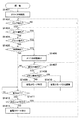
図2の説明に戻る。メモリバス201は、メモリコントローラ114と第1のRAM120及び第2のRAM121とを接続するための高速通信バスである。CPU112は、MFP100に電源が投入されると、システムバス111を介してROM113に格納されている起動プログラムを読み出し、MFP100を初期化するための初期化シーケンスを実行する。以下、起動プログラムによる第1のRAM120及び第2のRAM121の初期化シーケンスについて、図4のフローチャートを参照して説明する。
Returning to the description of FIG. The
図4は、MFP100に実装された第1のRAM120及び第2のRAM121の初期化シーケンスのフローチャートである。図4のフローチャートの各処理は、CPU112がROM113に格納されている起動プログラムを読み出し、第1のRAM120又は第2のRAM121に展開し、実行することによって実現される。なお、本実施形態では、第1のRAM120及び第2のRAM121以外のモジュールの初期化シーケンス及び制御シーケンスについての説明は省略する。また、ここでは、第1のRAM120及び第2のRAM121に限定されず、メモリデバイス(RAMに限る)としての説明を行い、適宜、第1のRAM120及び第2のRAM121に対する処理結果について説明することとする。
FIG. 4 is a flowchart of an initialization sequence of the
先ず、ステップS401において、CPU112は、シリアルバスを介して制御信号0,1(図2参照)により、メモリデバイスのメモリ情報を取得する。例えば、メモリモジュールに実装されているSPDからスペック情報を取得し、これにより、各メモリデバイスの電源制御が可能になる。なお、スペック情報とは、例えば、揮発性メモリか又は不揮発性メモリかに関する情報、最大クロック周波数、容量、信号タイミング等である。
First, in step S401, the
図5は、メモリモジュールのSPDから読み取ることができるメモリ情報の一例を示す図である。なお、図5に示したアドレスや値は一例であり、タイミングパラメータについても全ては記載されていない。CPU112は、SPDから読みとったメモリ情報の中から必要な情報を、例えば、不図示のHDDに記憶する。
FIG. 5 is a diagram illustrating an example of memory information that can be read from the SPD of the memory module. Note that the addresses and values shown in FIG. 5 are examples, and all timing parameters are not described. The
図5(a)は、第1のRAM120について取得したメモリ情報を示しており、読み取ったアドレスと値から、第1のRAM120は、DDR3 SDRAM、1066MHz、1Gbit、8bank、揮発性であることがわかる。図5(b)は、第2のRAM121について取得したメモリ情報を示しており、第2のRAM121は、DDR3 MRAM、1066MHz、1Gbit、8bank、不揮発性であることがわかる。
FIG. 5A shows the memory information acquired for the
次に、CPU112は、メモリコントローラ114に対してメモリ初期化のキャリブレーションの実行命令を発行する。これにより、ステップS402において、メモリコントローラ114は、メモリデバイスを初期化するキャリブレーションを実行する。具体的には、CPU112は、ステップS401での取得情報に基づき、メモリコントローラ114により、メモリ初期化時に実装されているメモリデバイスに対して、順次、アドレスをマッピングする。そして、CPU112は、メモリコントローラ114により、各メモリデバイスに対して、ライトレベリングとリードレベリングの両方のタイミング調整を行う。CPU112は、各メモリデバイスの各バンクのライトアクセス及びリードアクセス時のclk−dqs間のSkew情報とリードレイテンシを記憶する。
Next, the
図6は、第1のRAM120及び第2のRAM121の初期化キャリブレーションの結果の一例を示す図である。メモリコントローラ114による第1のRAM120及び第2のRAM121の初期化キャリブレーションが完了すると、CPU112は第1のRAM120及び第2のRAM121へアクセス可能となる。
FIG. 6 is a diagram illustrating an example of a result of initialization calibration of the
ステップS402の終了後、CPU112は、チップセレクト(以下「CS」と記す)毎にメモリマッピング処理を開始し、ステップS403において、メモリマッピング処理がなされていない残りのCSが有るか否かを判断する。CPU112は、残りCSが有る場合(S403でYES)、処理をステップS404へ進め、残りCSが無い場合(S403でNO)、処理をステップS410へ進める。
After the end of step S402, the
ステップS404において、CPU112は、ステップS403において選択したCSのメモリデバイスがDDR3 MRAM(不揮発性メモリ)であるか否かを、ステップS401で取得したメモリ情報に基づいて判断する。CPU112は、DDR3 MRAMである(不揮発性メモリである(S404でYES))場合、処理をステップS405へ進め、DDR3 MRAMではない(揮発性メモリである(S404でNO))場合、処理をステップS409へ進める。
In step S404, the
ステップS405において、CPU112は、選択したCSにF/W格納フラグが有るか否かを判断する。例えば、この判断は、メモリデバイスの先頭番地0x0に予め定めたフラグ値が格納されているか否かにより行われる。CPU112は、F/W格納フラグが有る場合(S405でYES)、処理をステップS406へ進め、F/W格納フラグが無い場合(S405でNO)、処理をステップS407へ進める。
In step S405, the
ステップS406において、CPU112は、F/W格納リスト及びF/W格納可能リストにCS情報を追加、格納する。その後、処理はステップS403へ戻される。
In step S406, the
ステップS407において、CPU112は、F/W格納容量が有るか否かを判断する。具体的には、CPU112は、ステップS401で取得したメモリ容量情報とROM113に予め格納されているF/W容量情報とを比較する。CPU112は、F/W格納容量が有る場合(S407でYES)、処理をステップS408へ進め、F/W格納容量が無い場合(S407でYES)、処理をステップS409へ進める。
In step S407, the
ステップS408において、CPU112は、F/W格納可能リストにCS情報を追加、格納する。ステップS409において、CPU112は、ワークメモリリストにCS情報を追加、格納する。ステップS408,S409の終了後、処理はステップS403へ戻される。
In step S408, the
図7は、MFP100のワークメモリリストの一例を示す図である。ステップS403〜S409の処理が全てのCSに対して終了すると、図7に示すワークメモリリストが得られる。本実施形態では、CS0及びCS1はそれぞれ、第1のRAM120及び第2のRAM121に該当するものとし、第2のRAM121にF/W格納フラグが書き込まれているものとする。第1のRAM120は揮発性メモリであるため、F/W格納リスト及びF/W格納可能リストのCS0に「No」が、ワークメモリリストのCS0に「Yes」がそれぞれ書き込まれる。一方、第2のRAM121は不揮発性メモリであり、F/W格納フラグが有るため、F/W格納リスト及びF/W格納可能リストのCS1に「Yes」が、ワークメモリリストのCS1に「No」がそれぞれ書き込まれる。
FIG. 7 is a diagram illustrating an example of a work memory list of the
ステップS403の判断がNoとなった後のステップS410において、CPU112は、図7のワークメモリリストからF/W格納リストに追加されたメモリが有る否かを判断する。CPU112は、追加されたメモリが有る場合(S410でYES)、処理をステップS411へ進め、追加されたメモリが無い場合(S410でNO)、処理をステップS415へ進める。
In step S410 after the determination in step S403 is No, the
ステップS411において、CPU112は、図7のワークメモリリストからF/W格納可能リストに追加されたメモリが有る否かを判断する。CPU112は、追加されたメモリが有る場合(S411でYES)、処理をステップS412へ進め、追加されたメモリが無い場合(S411でNO)、処理をステップS414へ進める。
In step S411, the
ステップS412において、CPU112は、F/W格納可能リストで「Yes」になっているCSを1つ選択し、F/W格納リストにそのCSのメモリデバイスを追加する。続くステップS413において、CPU112は、ステップS412で選択したCSのメモリデバイスの先頭番地0x0に予め定めたフラグ値を格納する。これにより、ステップS412においてF/W格納リストに追加されたメモリデバイスは、MFP100の次回の起動時には、ステップS405においてF/W格納フラグ有りとして検出されることとなる。
In step S412, the
ステップS414において、CPU112は、F/W格納フラグの有るメモリデバイスにF/Wを格納する。なお、F/Wは、ROM113又は不図示のHDD等の記憶媒体や、外部ネットワーク190のストレージに外部ネットワーク190経由で格納してもよい。ステップS414の後、処理はステップS415へ進められる。
In step S414, the
ステップS415において、CPU112は、図7のワークメモリリストにあるように、アドレスマッピングを実施する。具体的には、ステップS415では、F/Wが格納されているメモリデバイス(CS)に対して、起動プログラムがF/Wを実行する際に指定されているアドレス領域を割り当てる。本実施形態では、F/W実行アドレスが0x0000_0000であるとし、図7に示すように、CS1のDDR3 MRAM(第2のRAM121)に0x0000_0000が割り当てられる。F/W実行アドレスが割り当てられたメモリデバイス以外のメモリデバイスに対しては、ワークメモリとして使用されるアドレス領域が割り当てられる。本実施形態では、図7に示すように、CS0のDDR3 SDRAM(第1のRAM120)に0x8000_0000が割り当てられる。
In step S415, the
続くステップS416において、CPU112は、ステップS415で指定したアドレスからF/Wを実行し、その後、本処理は終了となる。
In the subsequent step S416, the
なお、本実施形態では、F/Wを不揮発性メモリ(DDR3 MRAM(第2のRAM121))に格納されるようにメモリマッピングを実施した。これに対して、例えば、MFP100において保持していなければならないファクシミリ画像データやページカウントデータ、トナー残量等のデータについても、同様の手法により不揮発性メモリに格納するようにしてもよい。また、揮発性メモリ(DDR3 SDRAM(第1のRAM120))には、一時的に使用される中間画像データ(例えば、MFP100が備える不図示のスキャナ部により読み取られたスキャンデータ)が格納されるようにしてもよい。
In the present embodiment, the memory mapping is performed so that the F / W is stored in the nonvolatile memory (DDR3 MRAM (second RAM 121)). On the other hand, for example, facsimile image data, page count data, and remaining toner amount data that must be held in the
ところで、不揮発性メモリである第2のRAM121の容量がF/Wを格納するのに十分でない場合が想定される。この場合、F/Wやその他の保持しておかなければならないプログラムやデータは、その他の不揮発性メモリ(例えば、フラッシュメモリ)やHDDがある場合には、これらにマッピングするようにする。また、第1のRAM120及び第2のRAM121の双方が揮発性メモリである場合、つまり、不揮発性メモリを備えない場合も想定される。この場合も、前述の不揮発性メモリの容量が足りない場合と同様の対処法が採られる。
By the way, the case where the capacity | capacitance of 2nd RAM121 which is a non-volatile memory is not enough to store F / W is assumed. In this case, F / W and other programs and data that must be retained are mapped to other nonvolatile memories (for example, flash memories) and HDDs, if any. In addition, it is assumed that both the
以上の説明の通り、本実施形態によれば、MFP100に不揮発性メモリと揮発性メモリとが混在して実装されていても、どのメモリデバイスが不揮発性メモリであるかを知ることができる。これにより、F/Wを不揮発性メモリにマッピングすることができるため、例えば、MFP100の省電力モード(スリープモード)への移行と省電力モードからの復帰に要する時間を短縮することができる。
As described above, according to the present embodiment, even if a non-volatile memory and a volatile memory are mixedly mounted on the
<第2実施形態>
上記第1実施形態では、初期化シーケンスのステップS401において、CPU112は、メモリモジュールに実装されているSPDからメモリデバイスのメモリ情報を入手し、そのメモリデバイスが不揮発性メモリであるか揮発性メモリであるかを判断している。これに対して、本実施形態では、SPDからのメモリ情報が無い場合に、リフレッシュコマンド間隔を変更することによりメモリデバイスが不揮発性メモリであるか揮発性メモリであるかを判断する。より具体的には、CPU112は、メモリデバイスに対して、一定時間以上、リフレッシュコマンドを発行しないことで、メモリデバイスが揮発性メモリであるか不揮発性メモリであるかを検出する。
Second Embodiment
In the first embodiment, in step S401 of the initialization sequence, the
図8は、リフレッシュコマンド間隔の変更を利用した不揮発性/揮発性メモリ検出シーケンスのフローチャートである。ここでも、第1のRAM120及び第2のRAM121に限定されず、メモリデバイス(RAMに限る)としての説明を行い、適宜、第1のRAM120及び第2のRAM121についての処理結果について説明することとする。
FIG. 8 is a flowchart of a non-volatile / volatile memory detection sequence using the change of the refresh command interval. Here, the description is not limited to the
ステップS801に先立って、図4のステップS402の処理が実行されるが、ステップS402の処理内容についてのここでの説明は省略する。ステップS402の後のステップS801において、CPU112は、CS毎にメモリタイプの判断(ステップS806)を実施していない残りのCSが有るか否かを判断する。CPU112は、残りCSが有る場合(S801でYES)、処理をステップS802へ進め、残りCSがない場合(S801でNO)、処理を終了させる。
Prior to step S801, the process of step S402 of FIG. 4 is executed, but the description of the process content of step S402 is omitted here. In step S801 after step S402, the
ステップS802において、CPU112は、ステップS801で残りCSとして選択したCSのメモリデバイスに対してテストデータを書き込む。例えば、複数のアドレスに特定パターンを書き込む。続くステップS803において、CPU112は、メモリコントローラ114に対してリフレッシュコマンドの発行間隔を変更する処理を実行する。例えば、揮発性メモリであるDDR3 SDRAMにおいては、放電で失った電荷を定期的に再充電する必要がある。そのために、JEDECのAverage Periodic Refresh Interval tREFI(0℃≦Tcase≦85℃)によれば、平均7.8μs以内にリフレッシュコマンドを発行しなければならない。この規定外ではデータを保持することは保証されないため、メモリコントローラ114は、平均で7.8μsに1度、リフレッシュコマンドを発行する。しかしながら、不揮発性メモリでは、リフレッシュコマンドを発行しなくてもデータを保持することができる。したがって、CPU112は、リフレッシュコマンドの発行を停止し又は発行間隔を10msのように十分大きい値に設定する。
In step S802, the
次に、ステップS804において、CPU112は、ステップS803で設定した時間以上の一定時間経過したか否かを判断する。CPU112は、一定時間が経過するまで待機し(S804でNO)、一定時間が経過すると(S804でYES)、処理をステップS805へ進める。ステップS805において、CPU112は、選択したCSのメモリデバイスから、ステップS802で書き込みを行ったアドレスの値を読み出して、書き込みデータと比較する。
Next, in step S804, the
次いで、ステップS806において、CPU112は、選択したCSのメモリタイプ判断、つまり、メモリデバイスが不揮発性メモリであるか否かの判断を行う。CPU112は、ステップS805での比較の結果、選択したCSのメモリデバイスは、全ての書き込みデータと読み出しデータとが一致している場合には不揮発性メモリであると判断し、一致しない場合は揮発性メモリであると判断する。その後、処理はステップS801へ戻される。
Next, in step S806, the
このような処理により、DDR3 SDRAMである第1のRAM120については、揮発性メモリであるとの判断がなされ、DDR3 MRAMである第2のRAM121については、不揮発性メモリであるとの判断がなされる。
By such processing, the
以上のリフレッシュコマンド間隔の変更を利用した不揮発性/揮発性メモリ検出シーケンスによれば、メモリデバイスが不揮発性か否かを判断することが可能となる。よって、MFP100に実装されたメモリデバイスに不揮発性メモリと揮発性メモリとが混在して実装されていても、F/Wを不揮発性メモリに確実にマッピングすることができる。これにより、第1実施形態と同じ効果が得られる。
According to the nonvolatile / volatile memory detection sequence using the change in the refresh command interval described above, it is possible to determine whether or not the memory device is nonvolatile. Therefore, even if the nonvolatile memory and the volatile memory are mixedly mounted on the memory device mounted on the
<第3実施形態>
本実施形態では、CPU112が、MFP100に実装されたメモリデバイス(第1のRAM120及び第2のRAM121)を検出した後に、省電力モード(スリープモード)に移行する際に、各メモリデバイスに対して行う電源制御処理について説明する。
<Third Embodiment>
In the present embodiment, the
図9は、MFP100のコントローラ部101において第1のRAM120及び第2のRAM121の電源制御を行う構成を示すブロック図である。図9に示す構成は、図2に示した構成に対して第1の電源スイッチ901及び第2の電源スイッチ902を付加した構成となっており、よって、図2と重複する部分の説明は省略する。
FIG. 9 is a block diagram illustrating a configuration in which the
第1の電源スイッチ901及び第2の電源スイッチ902はそれぞれ、設定によって第1のRAM120及び第2のRAM121に対する電源のON/OFFを切り替えることができる。CPU112は、第1実施形態での処理に加えて、制御信号2及び制御信号3により第1の電源スイッチ901及び第2の電源スイッチ902の設定を行うことで、第1のRAM120及び第2のRAM121の電源制御を行う。
The
図9に示した構成において、CPU112が、不揮発性メモリを検出して電源制御を行う方法について、図10及び図11を参照して説明する。図10は、電源制御メモリリストの初期化シーケンスのフローチャートである。また、図11は、図10のフローチャートの処理により作成される電源制御メモリリストの一例を示す図である。図10のフローチャートの各処理は、CPU112がROM113に格納されている起動プログラムを読み出し、第1のRAM120又は第2のRAM121に展開し、実行することによって実現される。
In the configuration shown in FIG. 9, a method in which the
なお、ここでも、第1のRAM120及び第2のRAM121に限定されず、メモリデバイス(RAMに限る)としての説明を行い、適宜、第1のRAM120及び第2のRAM121についての処理結果について説明することとする。また、ここでは、メモリデバイス以外の制御シーケンスについての説明は省略する。
In this case as well, the present invention is not limited to the
ステップS1001,S1002の処理は、先に図4を参照して説明したステップS401,402の処理と同じである。即ち、CPU112は、MFP100に電源が投入されると、第1実施形態で説明したように、システムバス111を介してROM113にある起動プログラムを実行する。これにより、CPU112は、メモリ情報を取得し、初期化シーケンスを実行する。このとき、第1の電源スイッチ901及び第2の電源スイッチ902は、常に電源ONの状態になっているものとする。
The processing in steps S1001 and S1002 is the same as the processing in steps S401 and 402 described above with reference to FIG. That is, when the
ステップS1003において、CPU112は、電源制御設定が行われていない残りのCSがあるか否かを判断する。CPU112は、残りCSが有る場合(S1003でYES)、処理をステップS1004へ進め、残りCSがない場合(S1003でNO)、処理を終了させる。ステップS1004において、CPU112は、ステップS1003において選択したCSにメモリモジュールが実装されているか否かを判断する。CPU112は、メモリモジュールが実装されている場合(S1004でYES)、処理をステップS1005へ進め、メモリモジュールが実装されていない場合(S1004でNO)、処理をステップS1009へ進める。
In step S1003, the
ステップS1005において、CPU112は、選択したCSのメモリデバイスがDDR3 MRAM(不揮発性メモリ)であるか否かを、ステップS1001で取得したメモリ情報に基づいて判断する。CPU112は、DDR3 MRAMである(不揮発性メモリである(S1005でYES))場合、処理をステップS1006へ進め、DDR3 MRAMではない(揮発性メモリである(S1005でNO))場合、処理をステップS1007へ進める。ステップS1007において、CPU112は、選択したCSのメモリデバイスにデータを格納するか否か(保持させるデータが有るか否か)を判断する。CPU112は、保持させるデータが有る場合(S1007でYES)、処理をステップS1008へ処理を進め、保持させるデータが無い場合(S1007でNO)、処理をステップS1006へ進める。
In step S1005, the
ステップS1006において、CPU112は、電源制御メモリリストの電源OFFメモリリスト欄に選択したCSのCS情報を追加(格納)する。ステップS1008において、CPU112は、電源制御メモリリストのセルフリフレッシュメモリリストに選択したCSのCS情報を追加する。ステップS1009において、CPU112は、選択したCSにメモリデバイスは実装されていないため、電源制御メモリリストの電源制御なしメモリリストにCS情報を追加する。CPU112は、ステップS1006,S1008,S1009の後、処理をステップS1003へ戻す。
In step S1006, the
本実施形態では、CS0及びCS1はそれぞれ第1のRAM120及び第2のRAM121に該当し、それ以外のCSにはメモリデバイスはなく、第1のRAM120がDDR3 SDRAMであって、第2のRAM121はDDR3 MRAMである。よって、図10の電源制御メモリリストの作成シーケンスによれば、図11に示す電源制御メモリリストが得られる。なお、電源制御メモリリストは、例えば、不図示のHDDに格納される。ここでは、ステップS1007の保持させるデータが有るか否かを起動時に判断したが、F/W起動後に同判断を行って、電源制御メモリリストを変更するようにしてもよい。
In the present embodiment, CS0 and CS1 correspond to the
上述の電源制御シーケンスは、MFP100に電源が投入されたときに、CPU112がメモリデバイスに対して実行するものであり、MFP100が省電力モードに入るときの電源制御シーケンスについて図12を参照して説明する。図12は、MFP100が省電力モードに入るときの電源制御シーケンスのフローチャートである。
The above-described power control sequence is executed by the
先ず、ステップS1201において、CPU112は、図10のフローチャートに従う初期化シーケンスで作成した電源制御メモリリストを参照して、メモリ情報を取得する。続くステップS1202において、CPU112は、CS毎に電源制御設定(ステップS1204,S1206,S1207のいずれか)が行われていない残りのCSが有るか否かを判断する。CPU112は、残りCSが有る場合(S1202でYES)、処理をステップS1203へ進め、残りCSが無い場合(S1202でNO)、本処理を終了させる。
First, in step S1201, the
ステップS1203において、CPU112は、選択したCSのメモリデバイスに対する電源OFFが可能か否かを、ステップS1201で取得したメモリ情報に基づき判断する。CPU112は、不揮発性メモリであるために電源OFFが可能な場合(S1203でYES)、処理をステップS1204へ進め、揮発性メモリであるために電源OFFが不可能な場合(S1203でNO)、処理をステップS1205へ進める。
In step S1203, the
ステップS1205において、CPU112は、選択したCSのメモリデバイスにセルフリフレッシュ設定が必要か否かを判断する。CPU112は、セルフリフレッシュ設定が必要な場合(S1205でYES)、処理をステップS1206へ進め、セルフリフレッシュ設定が不要な場合(S1205でNO)、処理をステップS1207へ進める。
In step S1205, the
ステップS1204において、CPU112は、選択したCSのメモリデバイスの電源をOFFにするために、電源スイッチ(第1の電源スイッチ901又は第2の電源スイッチ902)の設定を行う。これにより、MFP100が省電力モードに入るときには、選択したCSのメモリデバイスの電源はOFFにされる。
In step S1204, the
ステップS1206において、CPU112は、選択したCSのメモリデバイスをセルフリフレッシュモードに移行させるための設定をメモリコントローラ114に対して行う。これによりMFP100が省電力モードに入るときには、選択したCSのメモリデバイスは、セルフリフレッシュモードに移行される。なお、セルフリフレッシュを行わずに、メモリデバイスに保持されていたデータを不図示のHDD等に退避させて、電源をOFFにしてもよい。
In step S <b> 1206, the
ステップS1207において、CPU112は、選択したCSにはメモリデバイスが実装されておらず、電力消費が無いため、電源制御は行わない。ステップS1204,S1206,S1207の後、CPU112は、処理をステップS1202に戻す。
In step S1207, the
なお、MFP100が省電力モードから通常の動作モードに復帰するときには、CPU112は、電源OFFのメモリデバイスの電源スイッチに対して、電源をONにする設定を行う。よって、図11の電源制御メモリリストの場合、不揮発性メモリ(DDR3 MRAM)である第2のRAM121の第2の電源スイッチ902の電源がONされる。また、MFP100が省電力モードから通常の動作モードに復帰するときには、CPU112は、メモリコントローラ114を介して、セルフリフレッシュのメモリデバイス(図11の電源制御メモリリストではなし)を通常動作に復帰させる。
When the
本実施形態では、上述の通りに電源制御を行うことにより、MFP100が省電力モードにあるときの消費電力を小さく抑えることができる。
In the present embodiment, by performing power supply control as described above, power consumption when the
<第4実施形態>
第3実施形態では、第1実施形態と同様に、初期化シーケンスのステップS1001において、CPU112は、メモリモジュールに実装されているSPDからメモリ情報を入手し、メモリモジュールが不揮発性メモリであるか揮発性メモリであるかを判断している。これに対して、本実施形態では、実装されているメモリデバイスに対して電源を遮断し、一定時間経過後に再度、電源を通電したときにデータが保持されているかを確認することで、メモリデバイスが不揮発性メモリであるか揮発性メモリであるかを判断する。
<Fourth embodiment>
In the third embodiment, as in the first embodiment, in step S1001 of the initialization sequence, the
図13は、電源の遮断を利用した不揮発性/揮発性メモリ検出シーケンスのフローチャートである。図13の不揮発性/揮発性メモリ検出シーケンスは、初期化シーケンスのステップS1002(図10参照)の実行後に、起動プログラムによって実行される。なお、ここでも、第1のRAM120及び第2のRAM121に限定されず、メモリデバイス(但し、RAMに限る)としての説明を行い、適宜、第1のRAM120及び第2のRAM121についての処理結果について説明することとする。
FIG. 13 is a flowchart of a non-volatile / volatile memory detection sequence using power-off. The nonvolatile / volatile memory detection sequence in FIG. 13 is executed by the startup program after the execution of step S1002 (see FIG. 10) of the initialization sequence. Note that here, the description is not limited to the
先ず、ステップS1301において、CPU112は、メモリタイプの判断(ステップS1307)を行っていない残りのCSが有るか否かを判断する。CPU112は、残りCSが有る場合(S1301でYES)、処理をステップS1302へ進め、残りCSが無い場合(S1301でNO)、本処理を終了させる。ステップS1302において、CPU112は、ステップS1301で選択した残りCSのメモリデバイスに対してテストデータを書き込む。例えば、残りCSのメモリデバイスの複数のアドレスに特定パターンを書き込む。
First, in step S1301, the
続くステップS1303において、CPU112は、選択したCSのメモリデバイスの電源スイッチに電源OFFの設定を実行し、その結果、選択したCSのメモリデバイスに対する通電は停止される。その後、ステップS1304において、CPU112は、ステップS1303で設定した時間以上の一定時間が経過したかを判断し、一定時間が経過するまで待機する(S1304でNO)。CPU112は、一定時間が経過すると(S1304でYES)、処理をステップS1305へ進める。ステップS1305において、CPU112は、選択したCSのメモリデバイスの電源スイッチに電源ONの設定を実行し、これにより、選択したCSのメモリデバイスに対する通電が再開される。
In subsequent step S1303,
次に、ステップS1306において、CPU112は、選択したCSのメモリデバイスからステップS1302で書き込みを行ったアドレスの値を読み出し、書き込みデータと比較する。そして、ステップS1307において、CPU112は、選択したCSのメモリデバイスのメモリタイプを判断する。具体的には、CPU112は、ステップS1306での比較の結果に基づき、全ての書き込みデータと読み込みデータとが一致している場合には、選択したCSのメモリデバイスは不揮発性メモリであると判断する。一方、CPU112は、全ての書き込みデータと読み込みデータとが一致しない場合には、選択したCSのメモリデバイスは揮発性メモリデバイスであると判断する。ステップS1307の後、処理はステップS1301へ戻される。
Next, in step S1306, the
このような処理により、DDR3 SDRAMである第1のRAM120については、揮発性メモリであるとの判断がなされ、DDR3 MRAMである第2のRAM121については、不揮発性メモリであるとの判断がなされる。
By such processing, the
以上の電源の遮断を利用した不揮発性/揮発性メモリ検出シーケンスによれば、メモリデバイスが不揮発性か否かを判断することが可能となる。よって、MFP100に実装されたメモリデバイスに不揮発性メモリと揮発性メモリとが混在して実装されていても、省電力モードにあるときの消費電力を小さく抑えることができる。
According to the nonvolatile / volatile memory detection sequence using the above-described power-off, it is possible to determine whether or not the memory device is nonvolatile. Therefore, even when a non-volatile memory and a volatile memory are mixedly mounted on the memory device mounted on
<第5実施形態>
上記第1及び第2実施形態では、MFP100の起動時におけるメモリデバイスに対するマッピングについて、また、上記第3及び第4実施形態では、MFP100の起動時及び省電力モードへの移行時の電源制御処理について説明した。これに対して、本実施形態では、MFP100が備える各種機能(コピー機能、プリント機能、送信機能)の実行時における電源制御について、図14を参照して説明する。
<Fifth Embodiment>
In the first and second embodiments, the mapping to the memory device when the
図14は、MFP100の動作時における電源制御シーケンスのフローチャートである。図14のフローチャートの各処理は、CPU112がROM113に格納されている起動プログラムを読み出し、第1のRAM120又は第2のRAM121に展開し、実行することによって実現される。
FIG. 14 is a flowchart of a power supply control sequence during the operation of
MFP100が実行可能なコピー動作やプリント動作、送信動作等の各動作では、中間画像データ等を格納するためのワークメモリとして必要なメモリ容量が異なる。したがって、本実施形態では、各動作に必要なメモリ容量に応じて、メモリデバイスに対する電源の切り替え動作を実施することとし、図14のフローチャートは、そのキャリブレーション方法を示している。
In each operation such as a copy operation, a print operation, and a transmission operation that can be executed by the
MFP100に電源が投入されると、先ず、ステップS1401において、CPU112は、第1実施形態及び第3実施形態で説明した初期化シーケンスを実施する。これにより、F/Wが所定のメモリデバイスに格納され、また、電源制御メモリリストが作成(更新)されて、MFP100はスタンバイ状態となる。本実施形態では、第1のRAM120が揮発性メモリであるため、第1のRAM120に一時的に使用される中間画像データ等が保持されるものとする。また、第2のRAM121は不揮発性メモリであるため、第2のRAM121にF/Wが格納されるものとする。
When the
続くステップS1402において、CPU112は、ジョブが投入されたか否かを判定し、ジョブが投入されるまで待機し(S1402でNO)、ジョブが投入されると(S1402でYES)、処理をステップS1403へ進める。ステップS1403において、CPU112は、ジョブがコピー動作か否かを判断する。CPU112は、コピー動作である場合(S1403でYES)、処理をステップS1406へ進め、コピー動作ではない場合(S1403でNO)、処理をステップS1404へ進める。なお、コピー動作とは、MFP100のフィーダにセットされた原稿の画像をスキャナ部で取り込み、色変換や濃度変換、エッジ強調処理、スクリーン処理等の画像処理を施して、プリンタ部102で紙(シート)面上に画像形成し、出力する動作である。
In subsequent step S1402,
ステップS1404において、CPU112は、ジョブがプリント動作か否かを判断する。CPU112は、プリント動作である場合(S1404でYES)、処理をステップS1406へ進め、プリント動作ではない場合(S1404でNO)、処理をステップS1405へ進める。なお、プリント動作とは、ホストコンピュータ150や不図示のUSB等の外部装置から受信したPDLやJPEG等の画像データに対して、レンダリング処理や色変換、濃度変換、エッジ強調処理、スクリーン処理等の画像処理を実行し、プリンタ部102で紙(シート)面上に画像形成し、出力する動作である。
In step S1404, the
ステップS1405において、CPU112は、ジョブが送信動作か否かを判断する。CPU112は、送信動作である場合(S1405でYES)、処理をステップS1406へ進め、送信動作ではない場合(S1405でNO)、処理をステップS1411へ進める。なお、送信動作では、先ず、MFP100のフィーダにセットされた原稿の画像がスキャナ部で読み取られ、色変換や濃度変換、エッジ強調処理、圧縮処理等の画像処理が施されて、JPEG形式等のファイルが作成される。その後、作成されたファイルは、指定された電子メールアドレスにネットワークを介して送信され、或いは、モデムに接続された電話回線を通じて外部のファクシミリ装置へ送信される。なお、ステップS1403〜1405の各処理(判断)は、順序を問わず、どの判断が先に行われてもよい。
In step S1405, the
ステップS1406において、CPU112は、ステップS1403〜S1405のいずれかの処理に対して必要なワークメモリ領域(メモリ使用量)を計算する。CPU112は、コピー動作及び送信動作の場合には、中間画像データであるスキャンデータを一時保持するために、用紙サイズ等に基づきワークメモリ領域を計算する。プリント動作の場合、CPU112は、中間言語データやラスター画像データ等を一時保持するためのワークメモリ領域とプリント時に必要なワークメモリ領域とを、用紙サイズ等に基づいて計算する。その結果として、CPU112は、ステップS1401の初期化シーケンスで実行したメモリマッピングの結果に従って使用すべきメモリデバイスを選択する。
In step S1406, the
続くステップS1407において、CPU112は、第3実施形態に従って全てのCSのメモリデバイスに対して電源制御の設定を更新する処理を行い、処理が行われていない残りのCSが有るか否かを判断する。CPU112は、残りCSが有る場合(S1407でYES)、処理をステップS1408へ進め、残りCSが無い場合(S1407でNO)、処理をステップS1411へ進める。
In the following step S1407, the
ステップS1408において、CPU112は、ステップS1407で選択したCSのメモリデバイスが、ステップS1406において使用するメモリデバイスとして選択されているか否かを判断する。CPU112は、使用するメモリデバイスとして選択されていない場合(S1408でNO)、処理をステップS1409へ進め、使用するメモリデバイスとして選択されている場合(S1408でYES)、処理をステップS1410へ進める。
In step S1408, the
ステップS1409において、CPU112は、選択したCSのメモリデバイスは使用されないと判断し、第3実施形態のステップS1203〜S1207で実行した省電力モードへの移行処理を実施する。なお、このとき、各CSのメモリデバイスに対して電源がOFFされたとしても、他のメモリデバイスが動作することができるように、例えば、信号タイミングの調整等が行われる。ステップS1410において、CPU112は、選択したCSのメモリデバイスが省電力モードに入っていて電源がOFFとなっている場合には、省電力モードから通常の動作モードへ復帰させる。なお、ステップS1410では、選択したCSのメモリデバイスが通常の動作モードにあるときには、特に処理がおこなわれることはない。ステップS1409,S1410の後、CPU112は、処理をステップS1407へ戻す。
In step S1409, the
ステップS1411において、CPU112は、実行したジョブが終了したか否かを判断する。CPU112は、ジョブが終了するまで待機し(S1411でNO)、ジョブが終了すると(S1411でYES)、処理をステップS1412へ進める。ステップS1412において、CPU112は、次のジョブが有るか否かを判断する。CPU112は、次のジョブが有る場合(S1412でYES)、処理をステップS1403へ戻し、次のジョブが無い場合(S1412でNO)、処理をステップS1413へ進める。
In step S1411, the
ステップS1413において、CPU112は、全てのメモリデバイスに対して第3実施形態のステップS1203〜S1207で実行した省電力モードへの移行処理を実施する。その後、処理はステップS1402へ戻される。
In step S1413, the
以上の電源制御方法を用いて、ジョブが投入されたときでも不要なメモリデバイスを省電力モードに移行するようにすることで、MFP100の消費電力を低く抑えることができる。
By using the power supply control method described above to shift unnecessary memory devices to the power saving mode even when a job is submitted, the power consumption of the
<その他の実施形態>
以上、本発明をその好適な実施形態に基づいて詳述してきたが、本発明はこれら特定の実施形態に限られるものではなく、この発明の要旨を逸脱しない範囲の様々な形態も本発明に含まれる。更に、上述した各実施形態は本発明の一実施形態を示すものにすぎず、各実施形態を適宜組み合わせることも可能である。
<Other embodiments>
Although the present invention has been described in detail based on preferred embodiments thereof, the present invention is not limited to these specific embodiments, and various forms within the scope of the present invention are also included in the present invention. included. Furthermore, each embodiment mentioned above shows only one embodiment of this invention, and it is also possible to combine each embodiment suitably.
なお、第1実施形態では、MFP100を構成するモジュールをハードウェアとしてサポートした(図1参照)。これに対して、画像処理部119等の所定のモジュールについては、ROM113に格納されたプログラムをCPU112が実行することで、その機能が実現されるようにしてもよい。その場合、例えば、インタプリタ117、レンダラ118及び画像処理部119の機能を実現する各プログラムは、揮発性メモリへの各種データの読み込み/書き込み機能をサポートするものとする。
In the first embodiment, the modules constituting the
本発明は以下の処理を実行することによっても実現される。即ち、上述した実施形態の機能を実現するソフトウェア(プログラム)をネットワーク又は各種記憶媒体を介してシステム或いは装置に供給し、そのシステム或いは装置のコンピュータ(又はCPUやMPU等)がプログラムコードを読み出して実行する処理である。この場合、そのプログラム、及び該プログラムを記憶した記憶媒体は本発明を構成することになる。 The present invention can also be realized by executing the following processing. That is, software (program) that realizes the functions of the above-described embodiments is supplied to a system or apparatus via a network or various storage media, and a computer (or CPU, MPU, etc.) of the system or apparatus reads the program code. It is a process to be executed. In this case, the program and the storage medium storing the program constitute the present invention.
100 MFP
112 CPU
113 ROM
114 メモリコントローラ
120 第1のRAM
121 第2のRAM
901 第1の電源スイッチ
902 第2の電源スイッチ
100 MFP
112 CPU
113 ROM
114
121 Second RAM
901
Claims (8)
所定のデータが、前記検出手段が不揮発性メモリと検出した半導体メモリの中へ格納されるよう前記半導体メモリの設定を行う設定手段とを備えることを特徴とするメモリ制御装置。 Detecting means for detecting whether a semiconductor memory capable of writing and reading data is a nonvolatile memory or a volatile memory;
A memory control device comprising: a setting unit configured to set the semiconductor memory so that predetermined data is stored in the nonvolatile memory and the semiconductor memory detected by the detection unit.
データの書き込みと読み出しが可能な半導体メモリが不揮発性メモリであるか揮発性メモリであるかを検出する検出ステップと、
所定のデータが、前記検出ステップで不揮発性メモリと検出された半導体メモリの中へ格納されるよう前記半導体メモリの設定を行う設定ステップとを有することを特徴とするメモリ制御方法。 A memory control method executed by a computer,
A detection step of detecting whether the semiconductor memory capable of writing and reading data is a nonvolatile memory or a volatile memory;
A memory control method comprising: a setting step for setting the semiconductor memory so that predetermined data is stored in the nonvolatile memory and the semiconductor memory detected in the detection step .
データの書き込みと読み出しが可能な半導体メモリが不揮発性メモリであるか揮発性メモリであるかを検出する検出手段と、Detecting means for detecting whether a semiconductor memory capable of writing and reading data is a nonvolatile memory or a volatile memory;
所定のデータが、前記検出手段が不揮発性メモリと検出した半導体メモリの中へ格納されるよう前記半導体メモリの設定を行う設定手段と、して機能させることを特徴とするプログラム。A program for causing predetermined data to function as setting means for setting the semiconductor memory so that the detection means is stored in the non-volatile memory and the detected semiconductor memory.
Priority Applications (5)
| Application Number | Priority Date | Filing Date | Title |
|---|---|---|---|
| JP2013198330A JP6165008B2 (en) | 2013-09-25 | 2013-09-25 | MEMORY CONTROL DEVICE, MEMORY CONTROL METHOD, INFORMATION DEVICE, AND PROGRAM |
| KR1020140125697A KR101762242B1 (en) | 2013-09-25 | 2014-09-22 | Information processing apparatus, control method of information processing apparatus and non-transitory computer redable storage medium storing control program |
| CN201410491575.8A CN104464813A (en) | 2013-09-25 | 2014-09-23 | Memory control device, memory control method and information device |
| US14/494,943 US10268257B2 (en) | 2013-09-25 | 2014-09-24 | Memory control device that control semiconductor memory, memory control method, information device equipped with memory control device, and storage medium storing memory control program |
| EP14186091.6A EP2857979B1 (en) | 2013-09-25 | 2014-09-24 | Memory control device that controls semiconductory memory, memory control method, information device equipped with memory control device, and storage medium storing memory control program |
Applications Claiming Priority (1)
| Application Number | Priority Date | Filing Date | Title |
|---|---|---|---|
| JP2013198330A JP6165008B2 (en) | 2013-09-25 | 2013-09-25 | MEMORY CONTROL DEVICE, MEMORY CONTROL METHOD, INFORMATION DEVICE, AND PROGRAM |
Publications (3)
| Publication Number | Publication Date |
|---|---|
| JP2015064758A JP2015064758A (en) | 2015-04-09 |
| JP2015064758A5 JP2015064758A5 (en) | 2016-11-10 |
| JP6165008B2 true JP6165008B2 (en) | 2017-07-19 |
Family
ID=51655549
Family Applications (1)
| Application Number | Title | Priority Date | Filing Date |
|---|---|---|---|
| JP2013198330A Active JP6165008B2 (en) | 2013-09-25 | 2013-09-25 | MEMORY CONTROL DEVICE, MEMORY CONTROL METHOD, INFORMATION DEVICE, AND PROGRAM |
Country Status (5)
| Country | Link |
|---|---|
| US (1) | US10268257B2 (en) |
| EP (1) | EP2857979B1 (en) |
| JP (1) | JP6165008B2 (en) |
| KR (1) | KR101762242B1 (en) |
| CN (1) | CN104464813A (en) |
Families Citing this family (6)
| Publication number | Priority date | Publication date | Assignee | Title |
|---|---|---|---|---|
| WO2017107164A1 (en) * | 2015-12-25 | 2017-06-29 | 研祥智能科技股份有限公司 | Computer system of heterogeneous hybrid memory architecture and control method therefor, and memory detection system |
| US9830086B2 (en) * | 2016-03-03 | 2017-11-28 | Samsung Electronics Co., Ltd. | Hybrid memory controller for arbitrating access to volatile and non-volatile memories in a hybrid memory group |
| US11003381B2 (en) * | 2017-03-07 | 2021-05-11 | Samsung Electronics Co., Ltd. | Non-volatile memory storage device capable of self-reporting performance capabilities |
| US10650899B2 (en) * | 2017-04-27 | 2020-05-12 | Everspin Technologies, Inc. | Delayed write-back in memory with calibration support |
| JP7406895B2 (en) * | 2019-10-23 | 2023-12-28 | キヤノン株式会社 | Information processing device and method of controlling the information processing device |
| CN111190540B (en) * | 2019-12-25 | 2021-06-04 | 晶晨半导体(上海)股份有限公司 | Control method and device for write balance of memory interface |
Family Cites Families (40)
| Publication number | Priority date | Publication date | Assignee | Title |
|---|---|---|---|---|
| JPS58125125A (en) * | 1982-01-21 | 1983-07-26 | Toshiba Corp | Starting method of program |
| JPH04248641A (en) * | 1991-02-05 | 1992-09-04 | Sanyo Electric Co Ltd | Memory controller |
| US5918242A (en) * | 1994-03-14 | 1999-06-29 | International Business Machines Corporation | General-purpose customizable memory controller |
| KR0158489B1 (en) * | 1995-12-20 | 1998-12-15 | 김광호 | Discrimination method of semiconductor memory device |
| US6681286B2 (en) * | 2000-01-25 | 2004-01-20 | Via Technologies, Inc. | Control chipset having dual-definition pins for reducing circuit layout of memory slot |
| TW493119B (en) | 2001-03-28 | 2002-07-01 | Via Tech Inc | Method for automatically identifying the type of memory and motherboard using the same |
| US6989861B2 (en) * | 2001-09-14 | 2006-01-24 | Hewlett-Packard Development Company, L.P. | User selection of power-on configuration |
| US7627464B2 (en) * | 2002-04-18 | 2009-12-01 | Standard Microsystems Corporation | Bootable solid state floppy disk drive |
| EP1408510A3 (en) * | 2002-05-17 | 2005-05-18 | Matsushita Electric Industrial Co., Ltd. | Memory control apparatus, method and program |
| US7296171B2 (en) * | 2004-11-10 | 2007-11-13 | Microsoft Corporation | Selecting a power state based on predefined parameters |
| US20060245230A1 (en) * | 2005-04-29 | 2006-11-02 | Ambroggi Luca D | Memory module and method for operating a memory module |
| GB2426360A (en) * | 2005-05-18 | 2006-11-22 | Symbian Software Ltd | Reorganisation of memory for conserving power in a computing device |
| US7321524B2 (en) * | 2005-10-17 | 2008-01-22 | Rambus Inc. | Memory controller with staggered request signal output |
| WO2008040028A2 (en) * | 2006-09-28 | 2008-04-03 | Virident Systems, Inc. | Systems, methods, and apparatus with programmable memory control for heterogeneous main memory |
| US7594073B2 (en) * | 2006-09-29 | 2009-09-22 | Intel Corporation | Method and apparatus for caching memory content on a computing system to facilitate instant-on resuming from a hibernation state |
| JP2008129351A (en) * | 2006-11-21 | 2008-06-05 | Toshiba Corp | Image display device and image display method |
| US8396515B2 (en) * | 2007-11-30 | 2013-03-12 | Symbol Technologies, Inc. | Dynamic battery capacity allocation for data retention among mobile computers and electronic devices |
| US8738840B2 (en) * | 2008-03-31 | 2014-05-27 | Spansion Llc | Operating system based DRAM/FLASH management scheme |
| TWI375888B (en) | 2008-05-16 | 2012-11-01 | Phison Electronics Corp | Method, apparatus and controller for managing memories |
| US8169839B2 (en) * | 2009-02-11 | 2012-05-01 | Stec, Inc. | Flash backed DRAM module including logic for isolating the DRAM |
| US8977831B2 (en) * | 2009-02-11 | 2015-03-10 | Stec, Inc. | Flash backed DRAM module storing parameter information of the DRAM module in the flash |
| US8255620B2 (en) * | 2009-08-11 | 2012-08-28 | Texas Memory Systems, Inc. | Secure Flash-based memory system with fast wipe feature |
| US9110568B2 (en) * | 2009-10-13 | 2015-08-18 | Google Inc. | Browser tab management |
| JP5623090B2 (en) | 2010-01-29 | 2014-11-12 | キヤノン株式会社 | Information processing apparatus, control method for information processing apparatus, and control program |
| US8694812B2 (en) * | 2010-03-29 | 2014-04-08 | Dot Hill Systems Corporation | Memory calibration method and apparatus for power reduction during flash operation |
| JP2012033002A (en) * | 2010-07-30 | 2012-02-16 | Toshiba Corp | Memory management device and memory management method |
| JP5857549B2 (en) * | 2010-10-29 | 2016-02-10 | 株式会社リコー | Image processing apparatus, power saving return control method, power saving return control program, and recording medium |
| CN103562880A (en) * | 2011-05-26 | 2014-02-05 | 索尼爱立信移动通讯有限公司 | Optimized hibernate mode for wireless device |
| JP2013004043A (en) | 2011-06-22 | 2013-01-07 | Fuji Xerox Co Ltd | Information processing device, image forming apparatus, and program |
| US20130046934A1 (en) * | 2011-08-15 | 2013-02-21 | Robert Nychka | System caching using heterogenous memories |
| US9069551B2 (en) * | 2011-12-22 | 2015-06-30 | Sandisk Technologies Inc. | Systems and methods of exiting hibernation in response to a triggering event |
| EP2620838B1 (en) * | 2012-01-26 | 2015-04-22 | ST-Ericsson SA | Automatic partial array self-refresh |
| KR20140026889A (en) * | 2012-08-23 | 2014-03-06 | 삼성전자주식회사 | Resistive memory device performing selective refresh and method of refreshing the resistive memeory device |
| JP5787852B2 (en) * | 2012-09-07 | 2015-09-30 | 株式会社東芝 | Control device, information processing device, control method, and program |
| KR20150098649A (en) * | 2012-12-22 | 2015-08-28 | 퀄컴 인코포레이티드 | Reducing power consumption of volatile memory via use of non-volatile memory |
| US9032139B2 (en) * | 2012-12-28 | 2015-05-12 | Intel Corporation | Memory allocation for fast platform hibernation and resumption of computing systems |
| KR20140093505A (en) * | 2013-01-18 | 2014-07-28 | 삼성전자주식회사 | Method and apparatus for extending memory in terminal |
| US9286985B2 (en) * | 2013-02-12 | 2016-03-15 | Kabushiki Kaisha Toshiba | Semiconductor device with power mode transitioning operation |
| JP6087662B2 (en) * | 2013-02-28 | 2017-03-01 | 株式会社東芝 | Control device, control program, and information processing system |
| US20140281148A1 (en) * | 2013-03-15 | 2014-09-18 | Kabushiki Kaisha Toshiba | Memory system |
-
2013
- 2013-09-25 JP JP2013198330A patent/JP6165008B2/en active Active
-
2014
- 2014-09-22 KR KR1020140125697A patent/KR101762242B1/en active IP Right Grant
- 2014-09-23 CN CN201410491575.8A patent/CN104464813A/en active Pending
- 2014-09-24 US US14/494,943 patent/US10268257B2/en active Active
- 2014-09-24 EP EP14186091.6A patent/EP2857979B1/en active Active
Also Published As
| Publication number | Publication date |
|---|---|
| KR20150034096A (en) | 2015-04-02 |
| EP2857979B1 (en) | 2016-08-31 |
| US20150089267A1 (en) | 2015-03-26 |
| KR101762242B1 (en) | 2017-07-27 |
| CN104464813A (en) | 2015-03-25 |
| EP2857979A1 (en) | 2015-04-08 |
| US10268257B2 (en) | 2019-04-23 |
| JP2015064758A (en) | 2015-04-09 |
Similar Documents
| Publication | Publication Date | Title |
|---|---|---|
| JP6165008B2 (en) | MEMORY CONTROL DEVICE, MEMORY CONTROL METHOD, INFORMATION DEVICE, AND PROGRAM | |
| US10109328B2 (en) | Memory controller for adjusting timing based on memory power states | |
| JP2011040041A (en) | Control method of memory device for performing write leveling operation, write leveling method of memory device, memory controller performing write leveling operation, memory device and memory system | |
| JP2010218142A (en) | Data storage device and control method for data storage device | |
| JP2010194811A (en) | Printing device controller and printing device | |
| JP4298610B2 (en) | Data storage device | |
| US20130235419A1 (en) | Image forming apparatus and information processing apparatus | |
| TWI317519B (en) | Semiconductor memory, memory controller and control method for semiconductor memory | |
| JP2016051925A (en) | Information processing apparatus or the like including main system and sub system | |
| TW581966B (en) | Data processor | |
| SG186531A1 (en) | Data processing apparatus and image forming apparatus | |
| US10754415B2 (en) | Control apparatus that controls memory and control method thereof | |
| JP2007010970A (en) | Image display device and program for making computer execute image display method | |
| US20110292448A1 (en) | Program execution control method | |
| JP4882807B2 (en) | SDRAM control circuit and information processing apparatus | |
| JP6274774B2 (en) | Memory interface device and control method thereof | |
| JP5895640B2 (en) | Data processing device and memory control device | |
| US8631214B2 (en) | Memory control circuit, control method therefor, and image processing apparatus | |
| JP6700739B2 (en) | Controller and control method | |
| JP2008152315A (en) | Signal processing circuit | |
| KR102441459B1 (en) | Signal processing circuit | |
| JP2008117242A (en) | Data transfer control device and data transfer control method | |
| JP5919973B2 (en) | Electronic device and memory control method | |
| JP2008302583A (en) | Printing controlling circuit and image forming apparatus | |
| JP2010181998A (en) | Data processor |
Legal Events
| Date | Code | Title | Description |
|---|---|---|---|
| A521 | Request for written amendment filed |
Free format text: JAPANESE INTERMEDIATE CODE: A523 Effective date: 20160923 |
|
| A621 | Written request for application examination |
Free format text: JAPANESE INTERMEDIATE CODE: A621 Effective date: 20160923 |
|
| A977 | Report on retrieval |
Free format text: JAPANESE INTERMEDIATE CODE: A971007 Effective date: 20170516 |
|
| TRDD | Decision of grant or rejection written | ||
| A01 | Written decision to grant a patent or to grant a registration (utility model) |
Free format text: JAPANESE INTERMEDIATE CODE: A01 Effective date: 20170523 |
|
| A61 | First payment of annual fees (during grant procedure) |
Free format text: JAPANESE INTERMEDIATE CODE: A61 Effective date: 20170620 |
|
| R151 | Written notification of patent or utility model registration |
Ref document number: 6165008 Country of ref document: JP Free format text: JAPANESE INTERMEDIATE CODE: R151 |