EP2933893A1 - Active filter control device - Google Patents
Active filter control device Download PDFInfo
- Publication number
- EP2933893A1 EP2933893A1 EP13862658.5A EP13862658A EP2933893A1 EP 2933893 A1 EP2933893 A1 EP 2933893A1 EP 13862658 A EP13862658 A EP 13862658A EP 2933893 A1 EP2933893 A1 EP 2933893A1
- Authority
- EP
- European Patent Office
- Prior art keywords
- current
- phase
- command value
- active filter
- coordinate system
- Prior art date
- Legal status (The legal status is an assumption and is not a legal conclusion. Google has not performed a legal analysis and makes no representation as to the accuracy of the status listed.)
- Granted
Links
Images


Classifications
-
- F—MECHANICAL ENGINEERING; LIGHTING; HEATING; WEAPONS; BLASTING
- F25—REFRIGERATION OR COOLING; COMBINED HEATING AND REFRIGERATION SYSTEMS; HEAT PUMP SYSTEMS; MANUFACTURE OR STORAGE OF ICE; LIQUEFACTION SOLIDIFICATION OF GASES
- F25B—REFRIGERATION MACHINES, PLANTS OR SYSTEMS; COMBINED HEATING AND REFRIGERATION SYSTEMS; HEAT PUMP SYSTEMS
- F25B43/00—Arrangements for separating or purifying gases or liquids; Arrangements for vaporising the residuum of liquid refrigerant, e.g. by heat
- F25B43/003—Filters
-
- H—ELECTRICITY
- H02—GENERATION; CONVERSION OR DISTRIBUTION OF ELECTRIC POWER
- H02J—ELECTRIC POWER NETWORKS; CIRCUIT ARRANGEMENTS OR SYSTEMS FOR SUPPLYING OR DISTRIBUTING ELECTRIC POWER; SYSTEMS FOR STORING ELECTRIC ENERGY
- H02J3/00—Circuit arrangements for AC mains or AC distribution networks
- H02J3/01—Arrangements for reducing harmonics or ripples
-
- H—ELECTRICITY
- H02—GENERATION; CONVERSION OR DISTRIBUTION OF ELECTRIC POWER
- H02M—APPARATUS FOR CONVERSION BETWEEN AC AND AC, BETWEEN AC AND DC, OR BETWEEN DC AND DC, AND FOR USE WITH MAINS OR SIMILAR POWER SUPPLY SYSTEMS; CONVERSION OF DC OR AC INPUT POWER INTO SURGE OUTPUT POWER; CONTROL OR REGULATION THEREOF
- H02M1/00—Details of apparatus for conversion
- H02M1/14—Arrangements for reducing ripples from DC input or output
-
- H—ELECTRICITY
- H02—GENERATION; CONVERSION OR DISTRIBUTION OF ELECTRIC POWER
- H02M—APPARATUS FOR CONVERSION BETWEEN AC AND AC, BETWEEN AC AND DC, OR BETWEEN DC AND DC, AND FOR USE WITH MAINS OR SIMILAR POWER SUPPLY SYSTEMS; CONVERSION OF DC OR AC INPUT POWER INTO SURGE OUTPUT POWER; CONTROL OR REGULATION THEREOF
- H02M1/00—Details of apparatus for conversion
- H02M1/12—Arrangements for reducing harmonics from AC input or output
-
- Y—GENERAL TAGGING OF NEW TECHNOLOGICAL DEVELOPMENTS; GENERAL TAGGING OF CROSS-SECTIONAL TECHNOLOGIES SPANNING OVER SEVERAL SECTIONS OF THE IPC; TECHNICAL SUBJECTS COVERED BY FORMER USPC CROSS-REFERENCE ART COLLECTIONS [XRACs] AND DIGESTS
- Y02—TECHNOLOGIES OR APPLICATIONS FOR MITIGATION OR ADAPTATION AGAINST CLIMATE CHANGE
- Y02E—REDUCTION OF GREENHOUSE GAS [GHG] EMISSIONS, RELATED TO ENERGY GENERATION, TRANSMISSION OR DISTRIBUTION
- Y02E40/00—Technologies for an efficient electrical power generation, transmission or distribution
- Y02E40/40—Arrangements for reducing harmonics
Definitions
- the present invention relates to technology for controlling an active filter and, in particular, to technology for controlling a parallel active filter.
- harmonic component When load current flows from an AC power supply to a load, a so-called harmonic component is typically generated in the load current.
- the harmonic component is a well-known problem as it causes so-called harmonic interference, and is thus to be reduced.
- An active filter is proposed as one approach to solving the problem.
- a parallel active filter is connected to the AC power supply through an interconnection reactor and passing compensating current to reduce a harmonic component of power current flowing through the AC power supply.
- processing of passing compensating current of an opposite phase to this through the parallel active filter is performed.
- the harmonic component of the load current is adopted as a command value of the compensating current, and, based on a deviation of the compensating current therefrom, a current controller operates to control operation of the parallel active filter.
- the parallel active filter is introduced, for example, in Non-patent Document 1 and FIG. 10 of Patent Document 1.
- Patent Documents 2 and 3 are listed as prior art documents disclosing technology related to the present application.
- Patent Document 2 discloses technology for suppressing overcurrent in the event of accidents
- Patent Document 3 discloses technology for suppressing a time delay of operation of performing rotating coordinate conversion and a delay occurring when current is detected.
- Non-patent Document 1 Katsuhiro Izumi and four others, "Influence of the Compensation Current Detection Characteristic on the Active Filter Performance", Reports of the Faculty of Engineering, Nagasaki University, Vol. 30, No. 55, pp. 165-169, July 2000
- the parallel active filter is controlled by the operation of the current controller based on the deviation of current as described above.
- the current controller is typically configured as a proportional integral controller, and, due to arithmetic processing performed thereby, the compensating current tends to be delayed from the command value thereof. The divergence between the command value and the compensating current is likely to be more noticeable especially when the command value varies more significantly.
- Patent Documents 1 and 2 as well as Non-patent Document 1 are silent about such an impediment.
- the present invention has been conceived in view of the above-mentioned standpoint, and aims to provide technology for improving, in the active filter, the impediment to suppression of the harmonic component of the power current caused by the arithmetic processing performed by the current controller.
- An active filter control device is a device that controls a parallel active filter (6) connected, through an interconnection reactor (4), to an AC power supply (1) that supplies load current (Io) to a load (2), and outputting compensating current (Ic; Id, Iq).
- the first aspect thereof includes a harmonic component extraction unit (7A; 7B) obtaining a command value (Ic*; Id*, Iq*) of the compensating current from a harmonic component of the load current; a difference current generation unit (3A; 3B) obtaining a deviation (Ie) between the compensating current and a value (Ic* ⁇ ; Id* ⁇ , Iq* ⁇ ) obtained by leading a phase of the command value by a predetermined phase difference (360° ⁇ ta/Tr); a current controller (5; 10dd, 10qq) generating a control signal (V*; Vid, Viq) based on output of the difference current generation unit; and a driving signal generation circuit (8) generating, based on the control signal, a driving signal (G) driving the parallel active filter.
- a harmonic component extraction unit (7A; 7B) obtaining a command value (Ic*; Id*, Iq*) of the compensating current from a harmonic component of the load current
- the second aspect of the active filter control device is the first aspect, wherein the difference current generation unit (3A; 3B) includes: a delay unit (31) performing processing of delaying the command value (Ic*; Id*, Iq*) by a phase obtained by subtracting the predetermined phase difference (360° ⁇ ta/Tr) from a phase for one cycle of the AC power supply (1); and a subtracter (32) obtaining a difference between output (Ic* ⁇ ; Id* ⁇ , Iq* ⁇ ) of the delay unit and the compensating current (Ic; Id, Iq).
- the difference current generation unit (3A; 3B) includes: a delay unit (31) performing processing of delaying the command value (Ic*; Id*, Iq*) by a phase obtained by subtracting the predetermined phase difference (360° ⁇ ta/Tr) from a phase for one cycle of the AC power supply (1); and a subtracter (32) obtaining a difference between output (Ic* ⁇ ; Id* ⁇ , Iq* ⁇ ) of the delay
- the third aspect of the active filter control device is any one of the first aspect to the second aspect, wherein the command value (Ic*) is obtained by removing a DC component from the load current (Io) grasped in a rotating coordinate system synchronizing with a phase of the AC power supply (1), and further performing coordinate conversion so as to be grasped in a fixed coordinate system, the compensating current (Ic) is grasped in the fixed coordinate system, and the deviation (Ie) is obtained in the fixed coordinate system.
- the fourth aspect of the active filter control device is any one of the first aspect to the second aspect, wherein the command value (Id*, Iq*) is obtained by removing a DC component from the load current (Io) grasped in a rotating coordinate system synchronizing with a phase of the AC power supply (1), the compensating current (Id, Iq) is grasped in the rotating coordinate system, and the deviation (Ied, Ieq) is obtained in the rotating coordinate system.
- the fifth aspect of the active filter control device is the second aspect, wherein the load (2) is an air conditioner including: an inverter (23); and a compressor (24) controlled by the inverter to compress a refrigerant.
- the load (2) is an air conditioner including: an inverter (23); and a compressor (24) controlled by the inverter to compress a refrigerant.
- the phase of the command value of the compensating current is led by the predetermined phase difference to eliminate a delay time in the current controller.
- the phase difference can be set appropriately in accordance with the delay time.
- the phase of the command value can substantially be led by the delay unit as the command value varies with approximately the same waveform for each cycle of the AC power supply.
- a component, of the load current grasped in the rotating coordinate system, synchronizing with the phase of the AC power supply appears as a DC component. Therefore, by removing the DC component from the load current grasped in the rotating coordinate system, the harmonic component of the load current is obtained as the command value of the compensating current.
- the rotating coordinate system can be grasped as a two-phase coordinate system even when the AC power supply is a multi-phase power supply having three or more phases, and thus the configuration of the delay unit can easily be simplified.
- the cycles of the command value and the compensating current in the rotating coordinate system are shorter than those in the fixed coordinate system, and thus the configuration of the delay unit can easily be simplified when the delay unit is adopted.
- the variation of the load is small, and thus the delay unit substantially leads the phase of the command value with high accuracy.
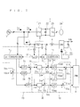
- FIG. 1 is a block diagram showing the aspect in which the active filter control device is adopted in the present embodiment. Description is made below by taking a case of adopting three-phase alternating current as an example. However, this number of phases is an example, and there is no need to limit the number of phases to three.
- a three-phase AC power supply 1 supplies three-phase load current Io to a load 2.
- a parallel active filter 6 is connected to the AC power supply 1 through a three-phase interconnection reactor 4.
- the parallel active filter 6 outputs three-phase compensating current Ic. Description is made herein on the assumption that a direction in which the compensating current Ic flows from the parallel active filter 6 to the AC power supply 1 is taken as being positive, and the sum of power current Is flowing from the AC power supply 1 and the compensating current Ic is equal to the load current Io.
- the parallel active filter 6 includes an inverter 61 and a capacitor 62, for example.
- the inverter 61 inputs and outputs the compensating current Ic to charge and discharge the capacitor 62 at a DC voltage Vdc.
- the inverter 61 is a voltage source inverter, three current paths are connected in parallel to the capacitor 62, and two switching elements are provided for each of the current paths.
- the active filter control device includes a harmonic component extraction unit 7A, a difference current generation unit 3A, a current controller 5, and a driving signal generation circuit 8.
- the harmonic component extraction unit 7A obtains a command value Ic* of the compensating current Ic from the harmonic component of the load current Io. Specific configuration is known from Patent Document 3 and other(s), so that description thereof is made only briefly.
- the harmonic component extraction unit 7A includes a transformer 71, a phase detector 72, a dq converter 73, high-pass filters 74 and 75, and an inverse dq converter 76.
- the transformer 71 detects one phase of a three-phase voltage Vs of the AC power supply 1, and provides it to the phase detector 72.
- the phase detector 72 transfers the detected phase to the dq converter 73 and the inverse dq converter 76.
- the dq converter 73 performs three-phase/two-phase conversion on the load current Io as detected to obtain d-axis current and q-axis current.
- the d-axis current and the q-axis current are provided to the inverse dq converter 76, after being removed low-frequency components, particularly DC components, by the high-pass filters 74 and 75.
- the inverse dq converter 76 performs two-phase/three-phase conversion to generate the command value Ic* of the compensating current Ic.
- the d axis and the q axis are herein axes in the rotating coordinate system rotating in synchronization with the phase detected by the phase detector 72.
- Components, of the load current Io, synchronizing with the phase of the AC power supply 1 appear as DC components in the d-axis current and the q-axis current. That is to say, the d-axis current and the q-axis current include only DC components in the absence of the harmonic component in the load current Io.
- the above-mentioned high-pass filters 74 and 75 thus output only the harmonic components of the load current Io, which appear as the d-axis current and the q-axis current.
- the command value Ic* represents the harmonic component of the load current Io. Therefore, when the compensating current Ic matches the command value Ic* with no phase shift, the compensating current Ic absorbs the harmonic component of the load current Io, and the harmonic component is not generated in the power current Is.
- the difference current generation unit 3A obtains a deviation Ie between the compensating current Ic and a value Ic* ⁇ obtained by leading a phase of the command value Ic* by a predetermined phase difference, which is described later.
- the command value Ic* is obtained by removing the DC component from the load current Io grasped in the rotating coordinate system (dq coordinate system) synchronizing with the phase of the AC power supply 1, and further performing coordinate conversion so as to be grasped in the fixed coordinate system.
- the compensating current Ic and the deviation Ie are also obtained in the fixed coordinate system.
- the current controller 5 performs processing of generating a three-phase voltage command value V* based on the output of the difference current generation unit 3A.
- the current controller 5 achieves the above-mentioned processing, for example, by performing PI (proportional integral) control.
- the driving signal generation circuit 8 generates, based on the voltage command value V*, a driving signal G driving the parallel active filter 6.
- the driving signal generation circuit 8 generates the driving signal G, for example, by performing logical operation on results of comparison between the voltage command value V* and a carrier. Therefore, it can be said that the voltage command value V* is a control signal indirectly controlling the parallel active filter 6 through the driving signal G.
- a delay time (hereinafter, this delay time is expressed as a time ta) occurs. If the deviation Ie is obtained from the command value Ic* and the compensating current Ic, the time ta causes a difference between the compensating current Ic and the harmonic component, and becomes an impediment to suppression of the harmonic component of the power current Is.
- the difference current generation unit 3A obtains the deviation Ie from the compensating current Ic and the value Ic* ⁇ obtained by leading the phase of the command value Ic* by a phase corresponding to the time ta to eliminate or reduce the above-mentioned impediment.
- the time ta is considered to take a constant value in a steady state. Therefore, the time ta can be estimated in advance through measurement or presumption, and the phase amount ⁇ can also be set in advance appropriately.
- the difference current generation unit 3A includes, for example, a delay unit 31 and a subtracter 32.
- the delay unit 31 performs processing of providing a delay by a phase obtained by subtracting the phase amount ⁇ from 360 degrees (i.e., a phase for one cycle unit of the voltage Vs). Since the harmonic component cyclically varies at the same cycle as the voltage Vs in the steady state, the delay becomes substantially equivalent to the phase leading by the phase amount ⁇ .
- the subtracter 32 obtains the deviation Ie as a difference between the output Ic* ⁇ of the delay unit 31 and the compensating current Ic.
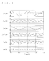
- FIGs. 2 to 4 and 6 are graphs showing the effects of the present embodiment.
- FIG. 5 is a graph showing the technology to be compared with the present embodiment.
- various amounts are shown for only one phase. This is because, in a case of adopting a balanced load as the load 2, three phases of the load current Io are balanced, three phases of each of the power current Is and the compensating current Ic are balanced, and three phases of each of these amounts only differ from one another by 120 degrees.
- FIG. 2 shows, downwards from an upper row, waveforms of the load current Io, a value (-Ic) obtained by reversing the polarity of the compensating current Ic, the power current Is, the phase-led command value Ic* ⁇ , the compensating current Ic, and the deviation Ie, respectively.
- FIG. 3 shows waveforms of the voltage Vs and its phase 0 in an upper row, a waveform of the command value Ic* in a middle row, and a waveform of the phase-led command value Ic* ⁇ in a lower row, respectively.
- the time ta and the cycle Tr are also shown. It is visually recognized that the command value Ic* ⁇ is led from the command value Ic* by the time ta.
- FIG. 4 shows waveforms of the command value Ic* and the phase-led command value Ic* ⁇ in an upper row and waveforms of the command value Ic* and the compensating current Ic in a lower row.
- the waveforms are shown in FIG. 4 in an extended time axis, compared to the waveforms shown in FIG. 3 . It is visually recognized from the waveforms in the upper row of FIG. 4 that the phase-led command value Ic* ⁇ is led from the command value Ic*, as visually recognized from the middle and lower rows of FIG. 3 . It is visually recognized from the waveforms in the lower row of FIG. 4 that the command value Ic* and the compensating current Ic have approximately the same waveform.
- FIG. 5 is a graph showing various amounts obtained when the delay amount in the delay unit 31 is set to 0 (i.e., the phase amount ⁇ is also set to 0). Waveforms of the (not phase-led) command value Ic* and the compensating current Ic are shown in an upper row, a waveform of the deviation Ie is shown in a middle row, and a waveform of the power current Is is shown in a lower row.
- FIG. 6 is a graph showing various amounts obtained when the delay unit 31 provides a delay substantially corresponding to the phase leading by the phase amount ⁇ . Waveforms of the phase-led command value Ic* ⁇ and the compensating current Ic are shown in an upper row, a waveform of the deviation Ie is shown in a middle row, and a waveform of the power current Is is shown in a lower row.
- FIG. 9 shows configuration obtained by omitting the delay unit 31 from FIG. 1 and substantially corresponding to configuration shown in FIG. 1 when the phase amount ⁇ is set to 0.
- FIG. 10 is a graph showing waveforms of various amounts obtained with the configuration so as to correspond to FIG. 2 .
- the impediment to suppression of the harmonic component of the power current Is caused by the arithmetic processing performed by the current controller can also be improved when the command value of the compensating current is grasped in the rotating coordinate system by performing phase leading in a similar manner to the first embodiment.
- FIG. 7 is a block diagram showing the aspect in which the active filter control device is adopted in the present embodiment.
- the harmonic component extraction unit 7A has been replaced by a harmonic component extraction unit 7B
- the difference current generation unit 3A has been replaced by a difference current generation unit 3B
- the current controller 5 has been replaced by a phase voltage command generation unit 10
- a dq converter 11 has been added in the configuration in the present embodiment.
- more detailed configuration of the load 2 is shown.
- the load 2 is an air conditioner including an inverter 23 and a compressor 24 controlled by the inverter 23 to compress a refrigerant (not shown).
- the load 2 further includes a converter 21 for supplying DC power to the inverter 23, and a capacitor 22 interposed in parallel between the converter 21 and the inverter 23.
- Such a load 2 is desirable as the variation of the load is small, and thus the phase of the command value is substantially led with high accuracy.
- the dq converter 11 performs dq conversion on the compensating current Ic, and outputs d-axis current Id and q-axis current Iq.
- the harmonic component extraction unit 7B has such configuration that the inverse dq conversion unit 76 has been omitted from the harmonic component extraction unit 7A, and a subtracter 77, a voltage controller 78, and an adder 79 have been added. Functions of and mutual connection relationships among the transformer 71, the phase detector 72, the dq converter 73, and the high-pass filters 74 and 75 of the harmonic component extraction unit 7B are the same as those of the harmonic component extraction unit 7A.
- the subtracter 77 obtains a deviation of the DC voltage Vdc supported by the capacitor 62 from the command value Vdc* thereof.
- the voltage controller 78 performs the PI control on the deviation obtained from the subtracter 77 to obtain a correction value of the d-axis current.
- the correction value is added to the output of the high-pass filter 74 (for the d-axis current) by the adder 79.
- a d-axis current command value Id* is obtained from the adder 79.
- a q-axis current command value Iq* is obtained from the high-pass filter 75 for the q-axis current. It can be said that the d-axis current command value Id* and the q-axis current command value Iq* are the harmonic components of the load current Io considering pulsation of the DC voltage Vdc as grasped in the rotating coordinate system. These can thus be grasped as command values of the d-axis current Id and the q-axis current Iq that are the compensating current Ic grasped in the rotating coordinate system.
- the difference current generation unit 3B includes delay units 31d and 31q, and subtracters 32d and 32q. Like the delay unit 31 shown in the first embodiment, each of the delay units 31 d and 31 q performs processing of providing a delay by a phase obtained by subtracting each of the phase amounts ⁇ d and ⁇ q from 360 degrees. These phase amounts ⁇ d and ⁇ q are described later.
- a phase-led d-axis current command value Id* ⁇ and a phase-led q-axis current command value Iq* ⁇ are respectively obtained from the d-axis current command value Id* and the q-axis current command value Iq* through the delay processing.
- the subtracters 32d and 32q respectively output deviations Ied and Ieq. That is to say, the deviation Ied between the phase-led d-axis current command value Id* ⁇ and the d-axis current Id as well as the deviation Ieq between the phase-led q-axis current command value Iq* ⁇ and the q-axis current Iq are respectively obtained from the subtracters 32d and 32q.
- the phase voltage command generation unit 10 includes current controllers 10dd and 10qq.
- the current controllers 10dd and 10qq respectively performs the PI control on the deviations Ied and Ieq to output voltage command values Vid and Viq.
- FIG. 7 shows the aspect in which configuration (hereinafter, referred to as "non-interference configuration") to avoid so-called interference between current control in the d-axis and current control in the q-axis is adopted, and the voltage command values Vid and Viq are corrected.
- the non-interference configuration is known technology as disclosed, for example, in Patent Document 2, so that description thereof is made only briefly.
- multipliers 10dq and 10qd have been additionally provided.
- the multiplier 10qd multiplies the product ⁇ L of the angular frequency ⁇ and the inductance L by the q-axis current command value Iq*, and provides it to the subtracter 10d.
- the subtracter 10d corrects the voltage command value Vid obtained from the current controller 10dd by subtracting the output of the multiplier 10qd.
- the adder 10q corrects the voltage command value Viq obtained from the current controller 10qq by adding the output of the multiplier 10dq.
- the (not phase-led) d-axis current command value Id* and q-axis current command value Iq* are respectively provided to the multipliers 10dq and 10qd. This is based on such a standpoint that a delay as in the processing performed by the current controllers 10dd and 10qq does not occur in the processing performed by the multipliers 10dq and 10qd.
- phase-led d-axis current command value Id* ⁇ and the phase-led q-axis current command value Iq* ⁇ may respectively be provided to the multipliers 10dq and 10qd.
- multipliers 10dq and 10qd, the subtracter 10d, and the adder 10q can naturally be omitted when interference between the d-axis and the q-axis is not considered.
- the driving signal generation circuit 8 generates, based on the voltage command values Vid and Viq for two phases, the driving signal G driving the parallel active filter 6, in contrast to the first embodiment. Therefore, it can also be said that the voltage command values Vid and Viq are control signals indirectly controlling the parallel active filter 6 through the driving signal G as with the voltage command value V* for three phases. Since the configuration of the driving signal generation circuit 8 having this function is well known, description thereof is omitted herein.
- FIG. 8 is a graph showing the effects of the second embodiment, and shows, downwards from an upper row, respective waveforms of the d-axis current Id, the deviation Ied, the q-axis current Iq, the deviation Ieq, and the power current Is in the stated order.
- the d-axis current Id cyclically varies at a cycle Tr/6, which is 1/6 of the cycle Tr of the power current Is, reflecting that the power current Is actually has three phases.
- the d-axis current Id is approximately sinusoidal.
- the q-axis current Iq also cyclically varies at the cycle Tr/6.
- the compensating current Ic is grasped as the d-axis current Id and the q-axis current Iq in the rotating coordinate system and the deviations Ied and Ieq are obtained in this rotating coordinate system. Since the rotating coordinate system can be grasped as a two-phase coordinate system even when the AC power supply 1 is a multi-phase power supply having three or more phases, the delay units 31 d and 31 q as well as the current controllers 10dd and 10qq for two phases are sufficient. In the first embodiment, the delay unit 31 and the current controller 5 are actually required for each of three phases.
- the d-axis current Id and the q-axis current Iq cyclically vary at a cycle that is 1/6 of the cycle Tr of the AC voltage Vs brings about other effects. That is to say, the cycles of the command values Id* and Iq* as well as the cycles of the d-axis current Id and the q-axis current Iq as the compensating current in the rotating coordinate system are shorter than the cycles Tr of them (the command value Ic* and the compensating current Ic in the first embodiment) in the fixed coordinate system. This easily simplifies the configuration in which the delay units 31 d and 31 q are adopted.
- FIFO memory used as the delay unit 31 shown in the first embodiment
- parts for the cycle Tr are sequentially stored, and sequentially output with the predetermined delay amount to substantially perform the phase-leading processing. Since the command value Ic* is stored for each of three phases in the example of the first embodiment, memory capacity that is three times larger than the cycle Tr is substantially required.
- the delay unit 31d in a case where the FIFO memory is used as the delay unit 31d, it suffices that the d-axis current command values Id* for the cycle Tr/6 are sequentially stored, and sequentially output with the predetermined delay amount. The same applies to the delay unit 31q.
- the required memory capacity is thus 1/3 of the cycle Tr, and can be reduced to 1/9 of that in the first embodiment.
- N the number of storage locations of the command value Ic* for one phase in the memory adopted as the delay unit 31 .
- the control cycle Tr when the number of storage locations for the cycle Tr is N, it is desirable that the control cycle be longer than N/Tr. It is also desirable to approximate the phase amount ⁇ by which the phase is led, which should originally be the time ta when converted into time, by k/(N ⁇ Tr) by introducing a non-negative integer k. This is because the phase-leading of the command value Ic* can be performed by delaying values for (N-k) data. The same applies to the delay units 31d and 31 q.
- integers k1 and k2 may be determined as shown below by expressing the fractional part of ta/Tr as F[ta/Tr], and a substantially phase-led command value may be obtained through interpolation using the (N-k1)th command value and the (N-k2)th command value.
Landscapes
- Engineering & Computer Science (AREA)
- Power Engineering (AREA)
- Chemical & Material Sciences (AREA)
- Analytical Chemistry (AREA)
- Physics & Mathematics (AREA)
- Mechanical Engineering (AREA)
- Thermal Sciences (AREA)
- General Engineering & Computer Science (AREA)
- Supply And Distribution Of Alternating Current (AREA)
- Inverter Devices (AREA)
- Rectifiers (AREA)
Abstract
Description
- The present invention relates to technology for controlling an active filter and, in particular, to technology for controlling a parallel active filter.
- When load current flows from an AC power supply to a load, a so-called harmonic component is typically generated in the load current. The harmonic component is a well-known problem as it causes so-called harmonic interference, and is thus to be reduced.
- An active filter is proposed as one approach to solving the problem. Particularly a parallel active filter is connected to the AC power supply through an interconnection reactor and passing compensating current to reduce a harmonic component of power current flowing through the AC power supply.
- Specifically, in order to reduce the harmonic component of the power current, processing of passing compensating current of an opposite phase to this through the parallel active filter (or supplying compensating current of the same phase as this from the parallel active filter) is performed.
- The harmonic component of the load current is adopted as a command value of the compensating current, and, based on a deviation of the compensating current therefrom, a current controller operates to control operation of the parallel active filter.
- The parallel active filter is introduced, for example, in
Non-patent Document 1 andFIG. 10 ofPatent Document 1. - Further,
Patent Documents Patent Document 2 discloses technology for suppressing overcurrent in the event of accidents, andPatent Document 3 discloses technology for suppressing a time delay of operation of performing rotating coordinate conversion and a delay occurring when current is detected. -
- Patent Document 1: Japanese Patent No.
3755220 - Patent Document 2: Japanese Patent Application Laid-open No.
5-252751 - Patent Document 3: Japanese Patent Application Laid-open No.
2008-234298 - Non-patent Document 1: Katsuhiro Izumi and four others, "Influence of the Compensation Current Detection Characteristic on the Active Filter Performance", Reports of the Faculty of Engineering, Nagasaki University, Vol. 30, No. 55, pp. 165-169, July 2000
- The parallel active filter is controlled by the operation of the current controller based on the deviation of current as described above. The current controller, however, is typically configured as a proportional integral controller, and, due to arithmetic processing performed thereby, the compensating current tends to be delayed from the command value thereof. The divergence between the command value and the compensating current is likely to be more noticeable especially when the command value varies more significantly.
- Such a delay caused by the arithmetic processing becomes an impediment to suppression of the harmonic component of the power current. However,
Patent Documents Document 1 are silent about such an impediment. - The present invention has been conceived in view of the above-mentioned standpoint, and aims to provide technology for improving, in the active filter, the impediment to suppression of the harmonic component of the power current caused by the arithmetic processing performed by the current controller.
- An active filter control device according to the present invention is a device that controls a parallel active filter (6) connected, through an interconnection reactor (4), to an AC power supply (1) that supplies load current (Io) to a load (2), and outputting compensating current (Ic; Id, Iq).
- The first aspect thereof includes a harmonic component extraction unit (7A; 7B) obtaining a command value (Ic*; Id*, Iq*) of the compensating current from a harmonic component of the load current; a difference current generation unit (3A; 3B) obtaining a deviation (Ie) between the compensating current and a value (Ic*^; Id*^, Iq*^) obtained by leading a phase of the command value by a predetermined phase difference (360° ×ta/Tr); a current controller (5; 10dd, 10qq) generating a control signal (V*; Vid, Viq) based on output of the difference current generation unit; and a driving signal generation circuit (8) generating, based on the control signal, a driving signal (G) driving the parallel active filter.
- The second aspect of the active filter control device according to the present invention is the first aspect, wherein the difference current generation unit (3A; 3B) includes: a delay unit (31) performing processing of delaying the command value (Ic*; Id*, Iq*) by a phase obtained by subtracting the predetermined phase difference (360°×ta/Tr) from a phase for one cycle of the AC power supply (1); and a subtracter (32) obtaining a difference between output (Ic*^; Id*^, Iq*^) of the delay unit and the compensating current (Ic; Id, Iq).
- The third aspect of the active filter control device according to the present invention is any one of the first aspect to the second aspect, wherein the command value (Ic*) is obtained by removing a DC component from the load current (Io) grasped in a rotating coordinate system synchronizing with a phase of the AC power supply (1), and further performing coordinate conversion so as to be grasped in a fixed coordinate system, the compensating current (Ic) is grasped in the fixed coordinate system, and the deviation (Ie) is obtained in the fixed coordinate system.
- The fourth aspect of the active filter control device according to the present invention is any one of the first aspect to the second aspect, wherein the command value (Id*, Iq*) is obtained by removing a DC component from the load current (Io) grasped in a rotating coordinate system synchronizing with a phase of the AC power supply (1), the compensating current (Id, Iq) is grasped in the rotating coordinate system, and the deviation (Ied, Ieq) is obtained in the rotating coordinate system.
- The fifth aspect of the active filter control device according to the present invention is the second aspect, wherein the load (2) is an air conditioner including: an inverter (23); and a compressor (24) controlled by the inverter to compress a refrigerant.
- According to the first aspect of the active filter control device according to the present invention, the phase of the command value of the compensating current is led by the predetermined phase difference to eliminate a delay time in the current controller. The phase difference can be set appropriately in accordance with the delay time.
- According to the second aspect of the active filter control device according to the present invention, the phase of the command value can substantially be led by the delay unit as the command value varies with approximately the same waveform for each cycle of the AC power supply.
- According to the third aspect of the active filter control device according to the present invention, a component, of the load current grasped in the rotating coordinate system, synchronizing with the phase of the AC power supply appears as a DC component. Therefore, by removing the DC component from the load current grasped in the rotating coordinate system, the harmonic component of the load current is obtained as the command value of the compensating current.
- According to the fourth aspect of the active filter control device according to the present invention, the rotating coordinate system can be grasped as a two-phase coordinate system even when the AC power supply is a multi-phase power supply having three or more phases, and thus the configuration of the delay unit can easily be simplified. The cycles of the command value and the compensating current in the rotating coordinate system are shorter than those in the fixed coordinate system, and thus the configuration of the delay unit can easily be simplified when the delay unit is adopted.
- According to the fifth aspect of the active filter control device according to the present invention, the variation of the load is small, and thus the delay unit substantially leads the phase of the command value with high accuracy.
- Objects, features, aspects and advantages of the present invention will become more apparent from the following detailed description and the accompanying drawings.
-
- [
FIG. 1 ] A block diagram showing the aspect in which the active filter control device is adopted in a first embodiment. - [
FIG. 2 ] A graph showing the effects of the first embodiment. - [
FIG. 3 ] A graph showing the effects of the first embodiment. - [
FIG. 4 ] A graph showing the effects of the first embodiment. - [
FIG. 5 ] A graph showing technology to be compared with the first embodiment. - [
FIG. 6 ] A graph showing the effects of the first embodiment. - [
FIG. 7 ] A block diagram showing the aspect in which the active filter control device is adopted in a second embodiment. - [
FIG. 8 ] A graph showing the effects of the second embodiment. - [
FIG. 9 ] A block diagram showing the technology to be compared with the first embodiment. - [
FIG. 10 ] A graph showing the technology to be compared with the first embodiment. -
FIG. 1 is a block diagram showing the aspect in which the active filter control device is adopted in the present embodiment. Description is made below by taking a case of adopting three-phase alternating current as an example. However, this number of phases is an example, and there is no need to limit the number of phases to three. - A three-phase
AC power supply 1 supplies three-phase load current Io to aload 2. A parallelactive filter 6 is connected to theAC power supply 1 through a three-phase interconnection reactor 4. The parallelactive filter 6 outputs three-phase compensating current Ic. Description is made herein on the assumption that a direction in which the compensating current Ic flows from the parallelactive filter 6 to theAC power supply 1 is taken as being positive, and the sum of power current Is flowing from theAC power supply 1 and the compensating current Ic is equal to the load current Io. - Of course, if the direction of the compensating current Ic is taken as being opposite to the direction in the description of the present embodiment, only the polarity sign (positive/negative) of the compensating current Ic changes.
- The parallel
active filter 6 includes aninverter 61 and acapacitor 62, for example. The inverter 61 inputs and outputs the compensating current Ic to charge and discharge thecapacitor 62 at a DC voltage Vdc. For example, theinverter 61 is a voltage source inverter, three current paths are connected in parallel to thecapacitor 62, and two switching elements are provided for each of the current paths. - The active filter control device includes a harmonic component extraction unit 7A, a difference
current generation unit 3A, acurrent controller 5, and a drivingsignal generation circuit 8. - The harmonic component extraction unit 7A obtains a command value Ic* of the compensating current Ic from the harmonic component of the load current Io. Specific configuration is known from
Patent Document 3 and other(s), so that description thereof is made only briefly. The harmonic component extraction unit 7A includes atransformer 71, aphase detector 72, adq converter 73, high-pass filters inverse dq converter 76. - The
transformer 71 detects one phase of a three-phase voltage Vs of theAC power supply 1, and provides it to thephase detector 72. Thephase detector 72 transfers the detected phase to thedq converter 73 and theinverse dq converter 76. - The
dq converter 73 performs three-phase/two-phase conversion on the load current Io as detected to obtain d-axis current and q-axis current. The d-axis current and the q-axis current are provided to theinverse dq converter 76, after being removed low-frequency components, particularly DC components, by the high-pass filters inverse dq converter 76 performs two-phase/three-phase conversion to generate the command value Ic* of the compensating current Ic. The d axis and the q axis are herein axes in the rotating coordinate system rotating in synchronization with the phase detected by thephase detector 72. - Components, of the load current Io, synchronizing with the phase of the
AC power supply 1 appear as DC components in the d-axis current and the q-axis current. That is to say, the d-axis current and the q-axis current include only DC components in the absence of the harmonic component in the load current Io. The above-mentioned high-pass filters - The difference
current generation unit 3A obtains a deviation Ie between the compensating current Ic and a value Ic*^ obtained by leading a phase of the command value Ic* by a predetermined phase difference, which is described later. The command value Ic* is obtained by removing the DC component from the load current Io grasped in the rotating coordinate system (dq coordinate system) synchronizing with the phase of theAC power supply 1, and further performing coordinate conversion so as to be grasped in the fixed coordinate system. The compensating current Ic and the deviation Ie are also obtained in the fixed coordinate system. - The
current controller 5 performs processing of generating a three-phase voltage command value V* based on the output of the differencecurrent generation unit 3A. Thecurrent controller 5 achieves the above-mentioned processing, for example, by performing PI (proportional integral) control. - The driving
signal generation circuit 8 generates, based on the voltage command value V*, a driving signal G driving the parallelactive filter 6. The drivingsignal generation circuit 8 generates the driving signal G, for example, by performing logical operation on results of comparison between the voltage command value V* and a carrier. Therefore, it can be said that the voltage command value V* is a control signal indirectly controlling the parallelactive filter 6 through the driving signal G. - It is desirable to provide a low-
pass filter 9 in terms of removing ripples of the compensating current Ic. Only the low-pass filter 9 for one phase is shown herein, but is actually provided for each of three phases. - Since the
current controller 5 generates the voltage command value V* by performing the PI control as described above, a delay time (hereinafter, this delay time is expressed as a time ta) occurs. If the deviation Ie is obtained from the command value Ic* and the compensating current Ic, the time ta causes a difference between the compensating current Ic and the harmonic component, and becomes an impediment to suppression of the harmonic component of the power current Is. - In the present embodiment, however, the difference
current generation unit 3A obtains the deviation Ie from the compensating current Ic and the value Ic*^ obtained by leading the phase of the command value Ic* by a phase corresponding to the time ta to eliminate or reduce the above-mentioned impediment. - The phase amount ϕ for the phase leading can be expressed as ϕ = 360°×ta/Tr by introducing a cycle Tr of the voltage Vs output from the
AC power supply 1. The time ta is considered to take a constant value in a steady state. Therefore, the time ta can be estimated in advance through measurement or presumption, and the phase amount ϕ can also be set in advance appropriately. - The difference
current generation unit 3A includes, for example, adelay unit 31 and asubtracter 32. Thedelay unit 31 performs processing of providing a delay by a phase obtained by subtracting the phase amount ϕ from 360 degrees (i.e., a phase for one cycle unit of the voltage Vs). Since the harmonic component cyclically varies at the same cycle as the voltage Vs in the steady state, the delay becomes substantially equivalent to the phase leading by the phase amount ϕ. Thesubtracter 32 obtains the deviation Ie as a difference between the output Ic*^ of thedelay unit 31 and the compensating current Ic. -
FIGs. 2 to 4 and6 are graphs showing the effects of the present embodiment.FIG. 5 is a graph showing the technology to be compared with the present embodiment. InFIGs. 2 to 6 , various amounts are shown for only one phase. This is because, in a case of adopting a balanced load as theload 2, three phases of the load current Io are balanced, three phases of each of the power current Is and the compensating current Ic are balanced, and three phases of each of these amounts only differ from one another by 120 degrees. -
FIG. 2 shows, downwards from an upper row, waveforms of the load current Io, a value (-Ic) obtained by reversing the polarity of the compensating current Ic, the power current Is, the phase-led command value Ic*^, the compensating current Ic, and the deviation Ie, respectively. -
FIG. 3 shows waveforms of the voltage Vs and itsphase 0 in an upper row, a waveform of the command value Ic* in a middle row, and a waveform of the phase-led command value Ic*^ in a lower row, respectively. The time ta and the cycle Tr are also shown. It is visually recognized that the command value Ic*^ is led from the command value Ic* by the time ta. -
FIG. 4 shows waveforms of the command value Ic* and the phase-led command value Ic*^ in an upper row and waveforms of the command value Ic* and the compensating current Ic in a lower row. The waveforms are shown inFIG. 4 in an extended time axis, compared to the waveforms shown inFIG. 3 . It is visually recognized from the waveforms in the upper row ofFIG. 4 that the phase-led command value Ic*^ is led from the command value Ic*, as visually recognized from the middle and lower rows ofFIG. 3 . It is visually recognized from the waveforms in the lower row ofFIG. 4 that the command value Ic* and the compensating current Ic have approximately the same waveform. -
FIG. 5 is a graph showing various amounts obtained when the delay amount in thedelay unit 31 is set to 0 (i.e., the phase amount ϕ is also set to 0). Waveforms of the (not phase-led) command value Ic* and the compensating current Ic are shown in an upper row, a waveform of the deviation Ie is shown in a middle row, and a waveform of the power current Is is shown in a lower row. -
FIG. 6 is a graph showing various amounts obtained when thedelay unit 31 provides a delay substantially corresponding to the phase leading by the phase amount ϕ. Waveforms of the phase-led command value Ic*^ and the compensating current Ic are shown in an upper row, a waveform of the deviation Ie is shown in a middle row, and a waveform of the power current Is is shown in a lower row. -
FIG. 9 shows configuration obtained by omitting thedelay unit 31 fromFIG. 1 and substantially corresponding to configuration shown inFIG. 1 when the phase amount ϕ is set to 0.FIG. 10 is a graph showing waveforms of various amounts obtained with the configuration so as to correspond toFIG. 2 . - It is visually recognized from comparison between
FIGs. 5 and 6 and comparison betweenFIGs. 2 and10 that the deviation Ie is reduced, and the harmonic component of the power current Is is thereby significantly reduced by obtaining the compensating current Ic through control using not the command value Ic but the phase-led command value Ic*^. - That is to say, it is known that the impediment to suppression of the harmonic component of the power current Is caused by the arithmetic processing performed by the
current controller 5 has been improved in the present embodiment. - The impediment to suppression of the harmonic component of the power current Is caused by the arithmetic processing performed by the current controller can also be improved when the command value of the compensating current is grasped in the rotating coordinate system by performing phase leading in a similar manner to the first embodiment.
-
FIG. 7 is a block diagram showing the aspect in which the active filter control device is adopted in the present embodiment. In contrast to the configuration shown in the block diagram ofFIG. 1 in the first embodiment, the harmonic component extraction unit 7A has been replaced by a harmoniccomponent extraction unit 7B, the differencecurrent generation unit 3A has been replaced by a differencecurrent generation unit 3B, and thecurrent controller 5 has been replaced by a phase voltagecommand generation unit 10, and adq converter 11 has been added in the configuration in the present embodiment. Furthermore, more detailed configuration of theload 2 is shown. - In the example of the present embodiment, the
load 2 is an air conditioner including aninverter 23 and acompressor 24 controlled by theinverter 23 to compress a refrigerant (not shown). Theload 2 further includes aconverter 21 for supplying DC power to theinverter 23, and acapacitor 22 interposed in parallel between theconverter 21 and theinverter 23. - Such a
load 2 is desirable as the variation of the load is small, and thus the phase of the command value is substantially led with high accuracy. - The
dq converter 11 performs dq conversion on the compensating current Ic, and outputs d-axis current Id and q-axis current Iq. - The harmonic
component extraction unit 7B has such configuration that the inversedq conversion unit 76 has been omitted from the harmonic component extraction unit 7A, and asubtracter 77, avoltage controller 78, and anadder 79 have been added. Functions of and mutual connection relationships among thetransformer 71, thephase detector 72, thedq converter 73, and the high-pass filters component extraction unit 7B are the same as those of the harmonic component extraction unit 7A. - The
subtracter 77 obtains a deviation of the DC voltage Vdc supported by thecapacitor 62 from the command value Vdc* thereof. Thevoltage controller 78 performs the PI control on the deviation obtained from thesubtracter 77 to obtain a correction value of the d-axis current. The correction value is added to the output of the high-pass filter 74 (for the d-axis current) by theadder 79. As a result, a d-axis current command value Id* is obtained from theadder 79. - A q-axis current command value Iq* is obtained from the high-
pass filter 75 for the q-axis current. It can be said that the d-axis current command value Id* and the q-axis current command value Iq* are the harmonic components of the load current Io considering pulsation of the DC voltage Vdc as grasped in the rotating coordinate system. These can thus be grasped as command values of the d-axis current Id and the q-axis current Iq that are the compensating current Ic grasped in the rotating coordinate system. - The difference
current generation unit 3B includesdelay units subtracters delay unit 31 shown in the first embodiment, each of thedelay units - Like the
subtracter 32 shown in the first embodiment, thesubtracters subtracters - The phase voltage
command generation unit 10 includes current controllers 10dd and 10qq. The current controllers 10dd and 10qq respectively performs the PI control on the deviations Ied and Ieq to output voltage command values Vid and Viq. Assuming that delay times td and tq respectively occur through the PI control performed by the current controllers 10dd and 10qq, effects similar to those obtained in the first embodiment can be obtained by setting the above-mentioned phase amounts ϕd and ϕq as follows:
- Further,
FIG. 7 shows the aspect in which configuration (hereinafter, referred to as "non-interference configuration") to avoid so-called interference between current control in the d-axis and current control in the q-axis is adopted, and the voltage command values Vid and Viq are corrected. The non-interference configuration is known technology as disclosed, for example, inPatent Document 2, so that description thereof is made only briefly. - Specifically, multipliers 10dq and 10qd, a
subtracter 10d, and anadder 10q have been additionally provided. The multiplier 10dq multiplies the product ωL of an angular frequency ω (= 2π/Tr) of the AC voltage Vs and inductance L of the interconnection reactor by the d-axis current command value Id*, and provides it to theadder 10q. The multiplier 10qd multiplies the product ωL of the angular frequency ω and the inductance L by the q-axis current command value Iq*, and provides it to thesubtracter 10d. Thesubtracter 10d corrects the voltage command value Vid obtained from the current controller 10dd by subtracting the output of the multiplier 10qd. Theadder 10q corrects the voltage command value Viq obtained from the current controller 10qq by adding the output of the multiplier 10dq. - Note that the (not phase-led) d-axis current command value Id* and q-axis current command value Iq* are respectively provided to the multipliers 10dq and 10qd. This is based on such a standpoint that a delay as in the processing performed by the current controllers 10dd and 10qq does not occur in the processing performed by the multipliers 10dq and 10qd.
- However, the influence of the non-interference configuration is small in the steady state, and the delay occurring in the
delay units - Note that the multipliers 10dq and 10qd, the
subtracter 10d, and theadder 10q can naturally be omitted when interference between the d-axis and the q-axis is not considered. - In the present embodiment, the driving
signal generation circuit 8 generates, based on the voltage command values Vid and Viq for two phases, the driving signal G driving the parallelactive filter 6, in contrast to the first embodiment. Therefore, it can also be said that the voltage command values Vid and Viq are control signals indirectly controlling the parallelactive filter 6 through the driving signal G as with the voltage command value V* for three phases. Since the configuration of the drivingsignal generation circuit 8 having this function is well known, description thereof is omitted herein. -
FIG. 8 is a graph showing the effects of the second embodiment, and shows, downwards from an upper row, respective waveforms of the d-axis current Id, the deviation Ied, the q-axis current Iq, the deviation Ieq, and the power current Is in the stated order. - The d-axis current Id cyclically varies at a cycle Tr/6, which is 1/6 of the cycle Tr of the power current Is, reflecting that the power current Is actually has three phases. The d-axis current Id is approximately sinusoidal. Similarly, the q-axis current Iq also cyclically varies at the cycle Tr/6.
- It is known that the harmonic component is suppressed as the deviations Ied and Ieq are small, and the power current Is is approximately sinusoidal.
- As described so far, it is known that the impediment to suppression of the harmonic component of the power current Is caused by the arithmetic processing performed by the current controllers 10dd and 10qq has been improved in the present embodiment as in the first embodiment.
- As described above, in the present embodiment, the compensating current Ic is grasped as the d-axis current Id and the q-axis current Iq in the rotating coordinate system and the deviations Ied and Ieq are obtained in this rotating coordinate system. Since the rotating coordinate system can be grasped as a two-phase coordinate system even when the
AC power supply 1 is a multi-phase power supply having three or more phases, thedelay units delay unit 31 and thecurrent controller 5 are actually required for each of three phases. - Further, in the present embodiment, particularly the fact that the d-axis current Id and the q-axis current Iq cyclically vary at a cycle that is 1/6 of the cycle Tr of the AC voltage Vs brings about other effects. That is to say, the cycles of the command values Id* and Iq* as well as the cycles of the d-axis current Id and the q-axis current Iq as the compensating current in the rotating coordinate system are shorter than the cycles Tr of them (the command value Ic* and the compensating current Ic in the first embodiment) in the fixed coordinate system. This easily simplifies the configuration in which the
delay units - Specifically, in a case where FIFO memory is used as the
delay unit 31 shown in the first embodiment, for example, parts for the cycle Tr are sequentially stored, and sequentially output with the predetermined delay amount to substantially perform the phase-leading processing. Since the command value Ic* is stored for each of three phases in the example of the first embodiment, memory capacity that is three times larger than the cycle Tr is substantially required. - On the other hand, in a case where the FIFO memory is used as the
delay unit 31d, it suffices that the d-axis current command values Id* for the cycle Tr/6 are sequentially stored, and sequentially output with the predetermined delay amount. The same applies to thedelay unit 31q. The required memory capacity is thus 1/3 of the cycle Tr, and can be reduced to 1/9 of that in the first embodiment. - Assume that the number of storage locations of the command value Ic* for one phase in the memory adopted as the
delay unit 31 is N. For example, if a control cycle of the current control is 50 µs when Tr = 20 ms (corresponding to a power supply frequency of 50 Hz) is satisfied, it is desirable to satisfy N ≥ 20ms/50µs = 400. - In contrast, when the number of storage locations for the cycle Tr is N, it is desirable that the control cycle be longer than N/Tr. It is also desirable to approximate the phase amount ϕ by which the phase is led, which should originally be the time ta when converted into time, by k/(N·Tr) by introducing a non-negative integer k. This is because the phase-leading of the command value Ic* can be performed by delaying values for (N-k) data. The same applies to the
delay units - Alternatively, when the above-mentioned integer k for the time ta corresponding to the led phase does not exist, integers k1 and k2 may be determined as shown below by expressing the fractional part of ta/Tr as F[ta/Tr], and a substantially phase-led command value may be obtained through interpolation using the (N-k1)th command value and the (N-k2)th command value. The same applies to the
delay units 
- While the present invention has been described in detail, the foregoing description is in all aspects illustrative and not restrictive. It is therefore understood that numerous modifications that have not been described can be devised without departing from the scope of the present invention.
Claims (5)
- An active filter control device that controls a parallel active filter (6) connected to an AC power supply (1) through an interconnection reactor (4) and outputting compensating current (Ic; Id, Iq), said AC power supply supplying load current (Io) to a load (2), said active filter control device comprising:a harmonic component extraction unit (7A; 7B) obtaining a command value (Ic*; Id*, Iq*) of said compensating current from a harmonic component of said load current;a difference current generation unit (3A; 3B) obtaining a deviation (Ie) between said compensating current and a value (Ic^; Id*^, Iq*^) obtained by leading a phase of said command value by a predetermined phase difference (360°×ta/Tr);a current controller (5; 10dd, 10qq) generating a control signal (V*; Vid, Viq) based on output of said difference current generation unit; anda driving signal generation circuit (8) generating, based on said control signal, a driving signal (G) driving said parallel active filter.
- The active filter control device according to claim 1, wherein
said difference current generation unit (3A; 3B) includes:a delay unit (31) performing processing of delaying said command value (Ic*; Id*, Iq*) by a phase obtained by subtracting said predetermined phase difference (360°×ta/Tr) from a phase for one cycle of said AC power supply (1); anda subtracter (32) obtaining a difference between output (Ic*^; Id*^, Iq*^) of said delay unit and said compensating current (Ic; Id, Iq). - The active filter control device according to any one of claims 1 to 2, wherein
said command value (Ic*) is obtained by removing a DC component from said load current (Io) grasped in a rotating coordinate system synchronizing with a phase of said AC power supply (1), and further performing coordinate conversion so as to be grasped in a fixed coordinate system,
said compensating current (Ic) is grasped in said fixed coordinate system, and
said deviation (Ie) is obtained in said fixed coordinate system. - The active filter control device according to any one of claims 1 to 2, wherein
said command value (Id*, Iq*) is obtained by removing a DC component from said load current (Io) grasped in a rotating coordinate system synchronizing with a phase of said AC power supply (1),
said compensating current (Id, Iq) is grasped in said rotating coordinate system, and
said deviation (Ied, Ieq) is obtained in said rotating coordinate system. - The active filter control device according to claim 2, wherein
said load (2) is an air conditioner including:an inverter (23); anda compressor (24) controlled by said inverter to compress a refrigerant.
Applications Claiming Priority (2)
| Application Number | Priority Date | Filing Date | Title |
|---|---|---|---|
| JP2012273744A JP5585643B2 (en) | 2012-12-14 | 2012-12-14 | Active filter control device |
| PCT/JP2013/081662 WO2014091915A1 (en) | 2012-12-14 | 2013-11-25 | Active filter control device |
Publications (3)
| Publication Number | Publication Date |
|---|---|
| EP2933893A1 true EP2933893A1 (en) | 2015-10-21 |
| EP2933893A4 EP2933893A4 (en) | 2016-07-27 |
| EP2933893B1 EP2933893B1 (en) | 2018-09-19 |
Family
ID=50934209
Family Applications (1)
| Application Number | Title | Priority Date | Filing Date |
|---|---|---|---|
| EP13862658.5A Active EP2933893B1 (en) | 2012-12-14 | 2013-11-25 | Active filter control device |
Country Status (6)
| Country | Link |
|---|---|
| US (1) | US9835364B2 (en) |
| EP (1) | EP2933893B1 (en) |
| JP (1) | JP5585643B2 (en) |
| CN (1) | CN104823346B (en) |
| ES (1) | ES2702601T3 (en) |
| WO (1) | WO2014091915A1 (en) |
Cited By (1)
| Publication number | Priority date | Publication date | Assignee | Title |
|---|---|---|---|---|
| EP3514931A4 (en) * | 2016-09-30 | 2020-05-27 | Daikin Industries, Ltd. | Control device for active filter |
Families Citing this family (14)
| Publication number | Priority date | Publication date | Assignee | Title |
|---|---|---|---|---|
| WO2014174667A1 (en) | 2013-04-26 | 2014-10-30 | 富士電機株式会社 | Resonance suppression device |
| CN104505837B (en) * | 2015-01-15 | 2016-06-29 | 信元瑞电气有限公司 | A kind of fast current tracking and controlling method controlling active filter based on PI |
| JP6443169B2 (en) * | 2015-03-26 | 2018-12-26 | ダイキン工業株式会社 | Control device |
| JP6461874B2 (en) * | 2015-09-14 | 2019-01-30 | ダイキン工業株式会社 | Judgment method of connection order, judgment method of phase loss |
| KR102499262B1 (en) * | 2015-10-14 | 2023-02-13 | 삼성전자주식회사 | Active filter and control method for the same, power monitoring system including the active filter |
| CN105633963B (en) * | 2016-02-29 | 2018-02-16 | 南京工业职业技术学院 | Parallel connection type active electric filter harmonic compensation current DC level suppression circuit |
| CN105846432B (en) * | 2016-06-08 | 2018-07-17 | 珠海万力达电气自动化有限公司 | A kind of control system of APF parallel runnings |
| JP6299831B1 (en) * | 2016-09-30 | 2018-03-28 | ダイキン工業株式会社 | Active filter device, air conditioning device, and air conditioning system |
| DE102017112958A1 (en) * | 2017-06-13 | 2018-12-13 | Wobben Properties Gmbh | Wind turbine with gearless generator and generator filter |
| CN107592096B (en) * | 2017-09-29 | 2020-06-16 | 苏州大学 | A Robust Bias Compensation Adaptive Filter Filtering Method |
| EP3883115A4 (en) * | 2018-11-14 | 2022-06-22 | Toshiba Mitsubishi-Electric Industrial Systems Corporation | CURRENT CONVERSION DEVICE |
| JP7078869B2 (en) * | 2020-10-19 | 2022-06-01 | ダイキン工業株式会社 | Power conversion system |
| CN112583381B (en) * | 2020-12-15 | 2022-07-15 | 北京理工大学 | An Adaptive Filtering Method Based on Bias Compensation Auxiliary Variables |
| US12015353B1 (en) * | 2021-07-12 | 2024-06-18 | Smart Wires Inc. | Attenuating harmonic current in power transmission lines |
Family Cites Families (30)
| Publication number | Priority date | Publication date | Assignee | Title |
|---|---|---|---|---|
| JPH0834669B2 (en) * | 1986-06-26 | 1996-03-29 | 三菱電機株式会社 | Harmonic suppressor |
| JPH0746917B2 (en) * | 1987-07-28 | 1995-05-17 | 三菱電機株式会社 | Control device for three-phase converter |
| JPH02118362A (en) * | 1988-10-26 | 1990-05-02 | Hitachi Ltd | Capacity control air conditioner |
| JP3312178B2 (en) | 1992-03-02 | 2002-08-05 | 株式会社日立製作所 | Control device for self-excited inverter |
| US5321598A (en) * | 1992-09-18 | 1994-06-14 | Westinghouse Electric Corp. | Three-phase active filter utilizing rotating axis transformation |
| US5355295A (en) * | 1993-08-19 | 1994-10-11 | Westinghouse Electric Corporation | Series-parallel active power line conditioner utilizing temporary link energy boosting for enhanced peak voltage regulation capability |
| JP2784134B2 (en) * | 1993-09-07 | 1998-08-06 | 三菱電機株式会社 | Active filter device |
| US5548165A (en) * | 1994-07-18 | 1996-08-20 | Regents Of The University Of Minnesota | Hybrid filter for reducing distortion in a power system |
| JPH09233701A (en) * | 1996-02-29 | 1997-09-05 | Hitachi Ltd | Active filter control device |
| JP3755220B2 (en) | 1996-08-09 | 2006-03-15 | ダイキン工業株式会社 | Active filter device and control method thereof |
| JP3798894B2 (en) * | 1997-09-29 | 2006-07-19 | 東京電力株式会社 | Harmonic compensation method |
| JP3887944B2 (en) * | 1998-05-01 | 2007-02-28 | 株式会社明電舎 | Active filter |
| US6882549B2 (en) * | 2001-03-21 | 2005-04-19 | Honeywell International Inc. | Active filter for power distribution system with selectable harmonic elimination |
| US6657322B2 (en) * | 2001-10-01 | 2003-12-02 | Rockwell Automation Technologies, Inc. | Control system for active power filters |
| JP3722048B2 (en) * | 2001-11-15 | 2005-11-30 | 日産自動車株式会社 | Motor control device |
| JP2003169481A (en) * | 2001-11-30 | 2003-06-13 | Daikin Ind Ltd | Power supply and air conditioner |
| JP3783695B2 (en) * | 2003-03-20 | 2006-06-07 | 日産自動車株式会社 | Motor control device |
| JP3928575B2 (en) * | 2003-04-07 | 2007-06-13 | 日産自動車株式会社 | Motor control device |
| JP4359546B2 (en) * | 2004-09-06 | 2009-11-04 | 株式会社豊田中央研究所 | AC motor control device |
| CN100364199C (en) * | 2005-07-06 | 2008-01-23 | 香港理工大学 | Single-phase active power filter using analog cascade controller |
| JP4079178B2 (en) * | 2006-04-19 | 2008-04-23 | ダイキン工業株式会社 | Power converter, control method therefor, and air conditioner |
| JP5025295B2 (en) | 2007-03-20 | 2012-09-12 | 東芝三菱電機産業システム株式会社 | Semiconductor power converter |
| JP4487008B2 (en) * | 2008-12-03 | 2010-06-23 | シャープ株式会社 | Power supply |
| JP4487009B2 (en) * | 2008-12-03 | 2010-06-23 | シャープ株式会社 | Power supply |
| CN101963787B (en) * | 2009-07-22 | 2012-08-08 | 河南森源电气股份有限公司 | Dual feedback loop control method of power active filter |
| US8363433B2 (en) * | 2009-09-09 | 2013-01-29 | Ge Energy Power Conversion Technology Limited | Hybrid conditioner for a power system |
| JP5128568B2 (en) * | 2009-09-30 | 2013-01-23 | 株式会社日立製作所 | Wind power generation system and control method |
| JP2011211815A (en) * | 2010-03-30 | 2011-10-20 | Kokusan Denki Co Ltd | Controller of permanent magnet motor |
| JP5644396B2 (en) * | 2010-08-06 | 2014-12-24 | 株式会社明電舎 | Harmonic current suppression device and harmonic current suppression method for power converter |
| CN202111474U (en) * | 2011-06-07 | 2012-01-11 | 浙江容大电力设备制造有限公司 | Closed-loop control system with rapid prediction response for active filter |
-
2012
- 2012-12-14 JP JP2012273744A patent/JP5585643B2/en active Active
-
2013
- 2013-11-25 US US14/651,718 patent/US9835364B2/en active Active
- 2013-11-25 EP EP13862658.5A patent/EP2933893B1/en active Active
- 2013-11-25 CN CN201380062979.9A patent/CN104823346B/en active Active
- 2013-11-25 WO PCT/JP2013/081662 patent/WO2014091915A1/en not_active Ceased
- 2013-11-25 ES ES13862658T patent/ES2702601T3/en active Active
Cited By (1)
| Publication number | Priority date | Publication date | Assignee | Title |
|---|---|---|---|---|
| EP3514931A4 (en) * | 2016-09-30 | 2020-05-27 | Daikin Industries, Ltd. | Control device for active filter |
Also Published As
| Publication number | Publication date |
|---|---|
| US9835364B2 (en) | 2017-12-05 |
| ES2702601T3 (en) | 2019-03-04 |
| EP2933893B1 (en) | 2018-09-19 |
| AU2013358270B2 (en) | 2016-01-07 |
| AU2013358270A1 (en) | 2015-06-11 |
| CN104823346B (en) | 2017-09-22 |
| EP2933893A4 (en) | 2016-07-27 |
| WO2014091915A1 (en) | 2014-06-19 |
| CN104823346A (en) | 2015-08-05 |
| JP5585643B2 (en) | 2014-09-10 |
| JP2014121145A (en) | 2014-06-30 |
| US20150323232A1 (en) | 2015-11-12 |
Similar Documents
| Publication | Publication Date | Title |
|---|---|---|
| EP2933893B1 (en) | Active filter control device | |
| EP2903147B1 (en) | Method for controlling power conversion apparatus | |
| EP2988414B1 (en) | Control device | |
| EP1921740B1 (en) | Power converter control | |
| EP2611019B1 (en) | Control apparatus for regenerative medium voltage inverter | |
| EP2922192A1 (en) | Power converter, power generating system, apparatus for controlling power converter, and method for controlling power converter | |
| CN109874373B (en) | Control device for active filter | |
| EP2706652B1 (en) | Regenerative inverter device and inverter device using power cell unit | |
| EP3522363A1 (en) | Control device for power converter | |
| EP3691105B1 (en) | Power conversion device | |
| EP3771086A1 (en) | Power conversion device and rotary machine driving system | |
| KR101929519B1 (en) | Three level neutral point clamped inverter system having imbalance capacitor voltages and its control method | |
| US9285410B2 (en) | Control circuit, and power generation device having the same | |
| EP4318917A1 (en) | Power conversion device and control device | |
| AU2013358270B9 (en) | Active filter control device | |
| JP2015027231A (en) | Active filter | |
| JP2014217206A (en) | Storage device | |
| JP6201386B2 (en) | Current estimation device | |
| JP2014128119A (en) | Inverter controller |
Legal Events
| Date | Code | Title | Description |
|---|---|---|---|
| PUAI | Public reference made under article 153(3) epc to a published international application that has entered the european phase |
Free format text: ORIGINAL CODE: 0009012 |
|
| 17P | Request for examination filed |
Effective date: 20150608 |
|
| AK | Designated contracting states |
Kind code of ref document: A1 Designated state(s): AL AT BE BG CH CY CZ DE DK EE ES FI FR GB GR HR HU IE IS IT LI LT LU LV MC MK MT NL NO PL PT RO RS SE SI SK SM TR |
|
| AX | Request for extension of the european patent |
Extension state: BA ME |
|
| DAX | Request for extension of the european patent (deleted) | ||
| A4 | Supplementary search report drawn up and despatched |
Effective date: 20160627 |
|
| RIC1 | Information provided on ipc code assigned before grant |
Ipc: H02M 1/12 20060101ALI20160621BHEP Ipc: F25B 43/00 20060101ALI20160621BHEP Ipc: H02M 7/12 20060101ALI20160621BHEP Ipc: H02J 3/01 20060101AFI20160621BHEP |
|
| GRAP | Despatch of communication of intention to grant a patent |
Free format text: ORIGINAL CODE: EPIDOSNIGR1 |
|
| STAA | Information on the status of an ep patent application or granted ep patent |
Free format text: STATUS: GRANT OF PATENT IS INTENDED |
|
| INTG | Intention to grant announced |
Effective date: 20180529 |
|
| GRAS | Grant fee paid |
Free format text: ORIGINAL CODE: EPIDOSNIGR3 |
|
| GRAA | (expected) grant |
Free format text: ORIGINAL CODE: 0009210 |
|
| STAA | Information on the status of an ep patent application or granted ep patent |
Free format text: STATUS: THE PATENT HAS BEEN GRANTED |
|
| AK | Designated contracting states |
Kind code of ref document: B1 Designated state(s): AL AT BE BG CH CY CZ DE DK EE ES FI FR GB GR HR HU IE IS IT LI LT LU LV MC MK MT NL NO PL PT RO RS SE SI SK SM TR |
|
| REG | Reference to a national code |
Ref country code: GB Ref legal event code: FG4D |
|
| REG | Reference to a national code |
Ref country code: CH Ref legal event code: EP |
|
| REG | Reference to a national code |
Ref country code: AT Ref legal event code: REF Ref document number: 1044368 Country of ref document: AT Kind code of ref document: T Effective date: 20181015 |
|
| REG | Reference to a national code |
Ref country code: IE Ref legal event code: FG4D |
|
| REG | Reference to a national code |
Ref country code: DE Ref legal event code: R096 Ref document number: 602013044037 Country of ref document: DE |
|
| REG | Reference to a national code |
Ref country code: SE Ref legal event code: TRGR |
|
| REG | Reference to a national code |
Ref country code: NL Ref legal event code: MP Effective date: 20180919 |
|
| PG25 | Lapsed in a contracting state [announced via postgrant information from national office to epo] |
Ref country code: FI Free format text: LAPSE BECAUSE OF FAILURE TO SUBMIT A TRANSLATION OF THE DESCRIPTION OR TO PAY THE FEE WITHIN THE PRESCRIBED TIME-LIMIT Effective date: 20180919 Ref country code: GR Free format text: LAPSE BECAUSE OF FAILURE TO SUBMIT A TRANSLATION OF THE DESCRIPTION OR TO PAY THE FEE WITHIN THE PRESCRIBED TIME-LIMIT Effective date: 20181220 Ref country code: LT Free format text: LAPSE BECAUSE OF FAILURE TO SUBMIT A TRANSLATION OF THE DESCRIPTION OR TO PAY THE FEE WITHIN THE PRESCRIBED TIME-LIMIT Effective date: 20180919 Ref country code: NO Free format text: LAPSE BECAUSE OF FAILURE TO SUBMIT A TRANSLATION OF THE DESCRIPTION OR TO PAY THE FEE WITHIN THE PRESCRIBED TIME-LIMIT Effective date: 20181219 Ref country code: BG Free format text: LAPSE BECAUSE OF FAILURE TO SUBMIT A TRANSLATION OF THE DESCRIPTION OR TO PAY THE FEE WITHIN THE PRESCRIBED TIME-LIMIT Effective date: 20181219 Ref country code: RS Free format text: LAPSE BECAUSE OF FAILURE TO SUBMIT A TRANSLATION OF THE DESCRIPTION OR TO PAY THE FEE WITHIN THE PRESCRIBED TIME-LIMIT Effective date: 20180919 |
|
| REG | Reference to a national code |
Ref country code: LT Ref legal event code: MG4D |
|
| PG25 | Lapsed in a contracting state [announced via postgrant information from national office to epo] |
Ref country code: HR Free format text: LAPSE BECAUSE OF FAILURE TO SUBMIT A TRANSLATION OF THE DESCRIPTION OR TO PAY THE FEE WITHIN THE PRESCRIBED TIME-LIMIT Effective date: 20180919 Ref country code: AL Free format text: LAPSE BECAUSE OF FAILURE TO SUBMIT A TRANSLATION OF THE DESCRIPTION OR TO PAY THE FEE WITHIN THE PRESCRIBED TIME-LIMIT Effective date: 20180919 Ref country code: LV Free format text: LAPSE BECAUSE OF FAILURE TO SUBMIT A TRANSLATION OF THE DESCRIPTION OR TO PAY THE FEE WITHIN THE PRESCRIBED TIME-LIMIT Effective date: 20180919 |
|
| REG | Reference to a national code |
Ref country code: ES Ref legal event code: FG2A Ref document number: 2702601 Country of ref document: ES Kind code of ref document: T3 Effective date: 20190304 |
|
| REG | Reference to a national code |
Ref country code: AT Ref legal event code: MK05 Ref document number: 1044368 Country of ref document: AT Kind code of ref document: T Effective date: 20180919 |
|
| PG25 | Lapsed in a contracting state [announced via postgrant information from national office to epo] |
Ref country code: AT Free format text: LAPSE BECAUSE OF FAILURE TO SUBMIT A TRANSLATION OF THE DESCRIPTION OR TO PAY THE FEE WITHIN THE PRESCRIBED TIME-LIMIT Effective date: 20180919 Ref country code: NL Free format text: LAPSE BECAUSE OF FAILURE TO SUBMIT A TRANSLATION OF THE DESCRIPTION OR TO PAY THE FEE WITHIN THE PRESCRIBED TIME-LIMIT Effective date: 20180919 Ref country code: CZ Free format text: LAPSE BECAUSE OF FAILURE TO SUBMIT A TRANSLATION OF THE DESCRIPTION OR TO PAY THE FEE WITHIN THE PRESCRIBED TIME-LIMIT Effective date: 20180919 Ref country code: RO Free format text: LAPSE BECAUSE OF FAILURE TO SUBMIT A TRANSLATION OF THE DESCRIPTION OR TO PAY THE FEE WITHIN THE PRESCRIBED TIME-LIMIT Effective date: 20180919 Ref country code: EE Free format text: LAPSE BECAUSE OF FAILURE TO SUBMIT A TRANSLATION OF THE DESCRIPTION OR TO PAY THE FEE WITHIN THE PRESCRIBED TIME-LIMIT Effective date: 20180919 Ref country code: PL Free format text: LAPSE BECAUSE OF FAILURE TO SUBMIT A TRANSLATION OF THE DESCRIPTION OR TO PAY THE FEE WITHIN THE PRESCRIBED TIME-LIMIT Effective date: 20180919 Ref country code: IS Free format text: LAPSE BECAUSE OF FAILURE TO SUBMIT A TRANSLATION OF THE DESCRIPTION OR TO PAY THE FEE WITHIN THE PRESCRIBED TIME-LIMIT Effective date: 20190119 |
|
| PG25 | Lapsed in a contracting state [announced via postgrant information from national office to epo] |
Ref country code: PT Free format text: LAPSE BECAUSE OF FAILURE TO SUBMIT A TRANSLATION OF THE DESCRIPTION OR TO PAY THE FEE WITHIN THE PRESCRIBED TIME-LIMIT Effective date: 20190119 Ref country code: SK Free format text: LAPSE BECAUSE OF FAILURE TO SUBMIT A TRANSLATION OF THE DESCRIPTION OR TO PAY THE FEE WITHIN THE PRESCRIBED TIME-LIMIT Effective date: 20180919 Ref country code: SM Free format text: LAPSE BECAUSE OF FAILURE TO SUBMIT A TRANSLATION OF THE DESCRIPTION OR TO PAY THE FEE WITHIN THE PRESCRIBED TIME-LIMIT Effective date: 20180919 |
|
| REG | Reference to a national code |
Ref country code: DE Ref legal event code: R097 Ref document number: 602013044037 Country of ref document: DE |
|
| REG | Reference to a national code |
Ref country code: CH Ref legal event code: PL |
|
| PLBE | No opposition filed within time limit |
Free format text: ORIGINAL CODE: 0009261 |
|
| STAA | Information on the status of an ep patent application or granted ep patent |
Free format text: STATUS: NO OPPOSITION FILED WITHIN TIME LIMIT |
|
| PG25 | Lapsed in a contracting state [announced via postgrant information from national office to epo] |
Ref country code: LU Free format text: LAPSE BECAUSE OF NON-PAYMENT OF DUE FEES Effective date: 20181125 Ref country code: MC Free format text: LAPSE BECAUSE OF FAILURE TO SUBMIT A TRANSLATION OF THE DESCRIPTION OR TO PAY THE FEE WITHIN THE PRESCRIBED TIME-LIMIT Effective date: 20180919 Ref country code: DK Free format text: LAPSE BECAUSE OF FAILURE TO SUBMIT A TRANSLATION OF THE DESCRIPTION OR TO PAY THE FEE WITHIN THE PRESCRIBED TIME-LIMIT Effective date: 20180919 |
|
| REG | Reference to a national code |
Ref country code: BE Ref legal event code: MM Effective date: 20181130 |
|
| REG | Reference to a national code |
Ref country code: IE Ref legal event code: MM4A |
|
| 26N | No opposition filed |
Effective date: 20190620 |
|
| PG25 | Lapsed in a contracting state [announced via postgrant information from national office to epo] |
Ref country code: LI Free format text: LAPSE BECAUSE OF NON-PAYMENT OF DUE FEES Effective date: 20181130 Ref country code: CH Free format text: LAPSE BECAUSE OF NON-PAYMENT OF DUE FEES Effective date: 20181130 |
|
| PG25 | Lapsed in a contracting state [announced via postgrant information from national office to epo] |
Ref country code: IE Free format text: LAPSE BECAUSE OF NON-PAYMENT OF DUE FEES Effective date: 20181125 Ref country code: SI Free format text: LAPSE BECAUSE OF FAILURE TO SUBMIT A TRANSLATION OF THE DESCRIPTION OR TO PAY THE FEE WITHIN THE PRESCRIBED TIME-LIMIT Effective date: 20180919 |
|
| PG25 | Lapsed in a contracting state [announced via postgrant information from national office to epo] |
Ref country code: BE Free format text: LAPSE BECAUSE OF NON-PAYMENT OF DUE FEES Effective date: 20181130 |
|
| PG25 | Lapsed in a contracting state [announced via postgrant information from national office to epo] |
Ref country code: MT Free format text: LAPSE BECAUSE OF NON-PAYMENT OF DUE FEES Effective date: 20181125 |
|
| PG25 | Lapsed in a contracting state [announced via postgrant information from national office to epo] |
Ref country code: HU Free format text: LAPSE BECAUSE OF FAILURE TO SUBMIT A TRANSLATION OF THE DESCRIPTION OR TO PAY THE FEE WITHIN THE PRESCRIBED TIME-LIMIT; INVALID AB INITIO Effective date: 20131125 Ref country code: MK Free format text: LAPSE BECAUSE OF NON-PAYMENT OF DUE FEES Effective date: 20180919 Ref country code: CY Free format text: LAPSE BECAUSE OF FAILURE TO SUBMIT A TRANSLATION OF THE DESCRIPTION OR TO PAY THE FEE WITHIN THE PRESCRIBED TIME-LIMIT Effective date: 20180919 |
|
| P01 | Opt-out of the competence of the unified patent court (upc) registered |
Effective date: 20230525 |
|
| PGFP | Annual fee paid to national office [announced via postgrant information from national office to epo] |
Ref country code: FR Payment date: 20250930 Year of fee payment: 13 |
|
| PGFP | Annual fee paid to national office [announced via postgrant information from national office to epo] |
Ref country code: DE Payment date: 20250930 Year of fee payment: 13 |
|
| PGFP | Annual fee paid to national office [announced via postgrant information from national office to epo] |
Ref country code: GB Payment date: 20251001 Year of fee payment: 13 |
|
| PGFP | Annual fee paid to national office [announced via postgrant information from national office to epo] |
Ref country code: IT Payment date: 20251022 Year of fee payment: 13 |
|
| PGFP | Annual fee paid to national office [announced via postgrant information from national office to epo] |
Ref country code: TR Payment date: 20251121 Year of fee payment: 13 |
|
| PGFP | Annual fee paid to national office [announced via postgrant information from national office to epo] |
Ref country code: SE Payment date: 20251001 Year of fee payment: 13 |
|
| PGFP | Annual fee paid to national office [announced via postgrant information from national office to epo] |
Ref country code: ES Payment date: 20251209 Year of fee payment: 13 |