EP2932594B1 - Tunable wide band driver amplifier - Google Patents
Tunable wide band driver amplifier Download PDFInfo
- Publication number
- EP2932594B1 EP2932594B1 EP13818898.2A EP13818898A EP2932594B1 EP 2932594 B1 EP2932594 B1 EP 2932594B1 EP 13818898 A EP13818898 A EP 13818898A EP 2932594 B1 EP2932594 B1 EP 2932594B1
- Authority
- EP
- European Patent Office
- Prior art keywords
- band
- frequency band
- amplification
- low
- circuit
- Prior art date
- Legal status (The legal status is an assumption and is not a legal conclusion. Google has not performed a legal analysis and makes no representation as to the accuracy of the status listed.)
- Active
Links
- 230000003321 amplification Effects 0.000 claims description 42
- 238000003199 nucleic acid amplification method Methods 0.000 claims description 42
- 239000003990 capacitor Substances 0.000 claims description 41
- 238000000034 method Methods 0.000 claims description 17
- 230000009467 reduction Effects 0.000 claims description 6
- 238000005516 engineering process Methods 0.000 description 7
- 238000004891 communication Methods 0.000 description 4
- 238000013461 design Methods 0.000 description 4
- 230000006870 function Effects 0.000 description 4
- 230000003287 optical effect Effects 0.000 description 3
- 230000002238 attenuated effect Effects 0.000 description 2
- 230000005540 biological transmission Effects 0.000 description 2
- 238000010168 coupling process Methods 0.000 description 2
- 238000005859 coupling reaction Methods 0.000 description 2
- 239000000835 fiber Substances 0.000 description 2
- 239000002245 particle Substances 0.000 description 2
- 229910001218 Gallium arsenide Inorganic materials 0.000 description 1
- 230000008901 benefit Effects 0.000 description 1
- 238000004590 computer program Methods 0.000 description 1
- 230000008878 coupling Effects 0.000 description 1
- 230000001419 dependent effect Effects 0.000 description 1
- 230000000694 effects Effects 0.000 description 1
- 238000009434 installation Methods 0.000 description 1
- 238000004519 manufacturing process Methods 0.000 description 1
- 238000012986 modification Methods 0.000 description 1
- 230000004048 modification Effects 0.000 description 1
- 230000002441 reversible effect Effects 0.000 description 1
- 230000001629 suppression Effects 0.000 description 1
- 238000012546 transfer Methods 0.000 description 1
Images
Classifications
-
- H—ELECTRICITY
- H03—ELECTRONIC CIRCUITRY
- H03G—CONTROL OF AMPLIFICATION
- H03G9/00—Combinations of two or more types of control, e.g. gain control and tone control
- H03G9/20—Combinations of two or more types of control, e.g. gain control and tone control in frequency-selective amplifiers
- H03G9/24—Combinations of two or more types of control, e.g. gain control and tone control in frequency-selective amplifiers having semiconductor devices
-
- H—ELECTRICITY
- H03—ELECTRONIC CIRCUITRY
- H03F—AMPLIFIERS
- H03F1/00—Details of amplifiers with only discharge tubes, only semiconductor devices or only unspecified devices as amplifying elements
- H03F1/08—Modifications of amplifiers to reduce detrimental influences of internal impedances of amplifying elements
- H03F1/22—Modifications of amplifiers to reduce detrimental influences of internal impedances of amplifying elements by use of cascode coupling, i.e. earthed cathode or emitter stage followed by earthed grid or base stage respectively
- H03F1/223—Modifications of amplifiers to reduce detrimental influences of internal impedances of amplifying elements by use of cascode coupling, i.e. earthed cathode or emitter stage followed by earthed grid or base stage respectively with MOSFET's
-
- H—ELECTRICITY
- H03—ELECTRONIC CIRCUITRY
- H03F—AMPLIFIERS
- H03F1/00—Details of amplifiers with only discharge tubes, only semiconductor devices or only unspecified devices as amplifying elements
- H03F1/42—Modifications of amplifiers to extend the bandwidth
-
- H—ELECTRICITY
- H03—ELECTRONIC CIRCUITRY
- H03F—AMPLIFIERS
- H03F1/00—Details of amplifiers with only discharge tubes, only semiconductor devices or only unspecified devices as amplifying elements
- H03F1/56—Modifications of input or output impedances, not otherwise provided for
- H03F1/565—Modifications of input or output impedances, not otherwise provided for using inductive elements
-
- H—ELECTRICITY
- H03—ELECTRONIC CIRCUITRY
- H03F—AMPLIFIERS
- H03F3/00—Amplifiers with only discharge tubes or only semiconductor devices as amplifying elements
- H03F3/189—High-frequency amplifiers, e.g. radio frequency amplifiers
- H03F3/19—High-frequency amplifiers, e.g. radio frequency amplifiers with semiconductor devices only
- H03F3/193—High-frequency amplifiers, e.g. radio frequency amplifiers with semiconductor devices only with field-effect devices
-
- H—ELECTRICITY
- H03—ELECTRONIC CIRCUITRY
- H03F—AMPLIFIERS
- H03F3/00—Amplifiers with only discharge tubes or only semiconductor devices as amplifying elements
- H03F3/20—Power amplifiers, e.g. Class B amplifiers, Class C amplifiers
- H03F3/24—Power amplifiers, e.g. Class B amplifiers, Class C amplifiers of transmitter output stages
- H03F3/245—Power amplifiers, e.g. Class B amplifiers, Class C amplifiers of transmitter output stages with semiconductor devices only
-
- H—ELECTRICITY
- H03—ELECTRONIC CIRCUITRY
- H03F—AMPLIFIERS
- H03F2200/00—Indexing scheme relating to amplifiers
- H03F2200/06—A balun, i.e. balanced to or from unbalanced converter, being present at the input of an amplifier
-
- H—ELECTRICITY
- H03—ELECTRONIC CIRCUITRY
- H03F—AMPLIFIERS
- H03F2200/00—Indexing scheme relating to amplifiers
- H03F2200/111—Indexing scheme relating to amplifiers the amplifier being a dual or triple band amplifier, e.g. 900 and 1800 MHz, e.g. switched or not switched, simultaneously or not
-
- H—ELECTRICITY
- H03—ELECTRONIC CIRCUITRY
- H03F—AMPLIFIERS
- H03F2200/00—Indexing scheme relating to amplifiers
- H03F2200/36—Indexing scheme relating to amplifiers the amplifier comprising means for increasing the bandwidth
-
- H—ELECTRICITY
- H03—ELECTRONIC CIRCUITRY
- H03F—AMPLIFIERS
- H03F2200/00—Indexing scheme relating to amplifiers
- H03F2200/378—A variable capacitor being added in the output circuit, e.g. collector, drain, of an amplifier stage
-
- H—ELECTRICITY
- H03—ELECTRONIC CIRCUITRY
- H03F—AMPLIFIERS
- H03F2200/00—Indexing scheme relating to amplifiers
- H03F2200/387—A circuit being added at the output of an amplifier to adapt the output impedance of the amplifier
-
- H—ELECTRICITY
- H03—ELECTRONIC CIRCUITRY
- H03F—AMPLIFIERS
- H03F2200/00—Indexing scheme relating to amplifiers
- H03F2200/39—Different band amplifiers are coupled in parallel to broadband the whole amplifying circuit
-
- H—ELECTRICITY
- H03—ELECTRONIC CIRCUITRY
- H03F—AMPLIFIERS
- H03F2200/00—Indexing scheme relating to amplifiers
- H03F2200/391—Indexing scheme relating to amplifiers the output circuit of an amplifying stage comprising an LC-network
-
- H—ELECTRICITY
- H03—ELECTRONIC CIRCUITRY
- H03F—AMPLIFIERS
- H03F2200/00—Indexing scheme relating to amplifiers
- H03F2200/534—Transformer coupled at the input of an amplifier
Definitions
- the present application relates generally to the operation and design of analog front ends, and more particularly, to the operation and design of driver amplifiers for use in analog front ends.
- a conventional transmitter used in a wireless device may include multiple driver amplifiers (DA) to amplify signals in both low frequency and high frequency bands, respectively.
- DA driver amplifiers
- Having a dedicated DA for a specified frequency band may achieve the desired amplification goals; however such an implementation also may have several disadvantages.
- utilizing multiple DAs may result in increased costs in terms of die area requirements.
- other circuitry in the transmitter such as an up-converter, may need to be modified to support multiple DA configurations, thereby increasing the complexity of the transmitter.
- the power amplifier device comprises a power amplifier and an impedance matching circuit, switchable by means of a PIN-diode, which provides a load impedance adapted to each individual basic frequency band.
- the power amplifier device comprises a filter device comprising a fixed low-pass filter and a switchable filter acting as an engageable and disengageable notch filter, which comprises at least one reversible PIN-diode.
- This switchable filter allows to pass, in a first mode, signals in the first basic frequency band and suppresses at the same time at least one order of harmonics corresponding to this basic frequency band.
- a second mode the second basic frequency band is transmitted, and harmonics are suppressed by the fixed low-pass filter.
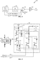
- FIG. 1 shows a transmitter 100 for use in a device that includes an exemplary embodiment of a novel tunable wide band DA 106.
- the transmitter 100 comprises a baseband processor 102 that outputs baseband data to be transmitted to an up-converter 104.
- the up-converter 104 up-converts the baseband data to a radio frequency (RF) signal and inputs this RF signal to the tunable wide band DA 106.
- the tunable DA 106 is configured to provide amplification over a wide frequency range (i.e., 800Mhz to 2.4GHz) that is divided into two selectable frequency bands.
- the tunable DA 106 receives a band select signal 110 from the baseband processor 102.
- the band select signal 110 selects one of the two selectable bands over which amplification will be provided.
- the tunable DA 106 also receives a trap enable signal 112 from the baseband processor 102.
- the trap enable signal 112 enables or disables a trap circuit that provides attenuation of 2 nd harmonic and higher frequencies for the amplified output.
- the amplified output of the tunable DA 106 is then input to a power amplifier (PA) 108 where the RF signal is further amplified for transmission.
- PA power amplifier
- the tunable DA 106 provides amplification over a wide frequency range and is configured to reduce die area by half when compared to conventional DA configurations that utilize multiple amplifiers.
- FIG. 2 shows a detailed exemplary embodiment of the tunable wide band driver amplifier 106 illustrated in FIG. 1 .
- the upconverter 104 outputs a differential signal to a balun 202 that converts the differential signal to a single-ended signal.
- the single-ended signal is input to transistor 204 of the DA 106.
- the transistor 204 operates with transistor 206 to amplify the single-ended signal to generate an amplified output signal (DA output) at the drain terminal 208 of transistor 206.
- DA output amplified output signal
- a first band selection circuit 238 operates to set the amplification band of the amplifier to a first frequency band.
- the first frequency band (also referred to herein as the low frequency band) has a center frequency designated as ( f LB ) .
- the first band selection circuit 238 comprises an inductor L LOW 210 and variable capacitor 212.
- the inductor L LOW 210 is connected between the drain terminal 208 and a supply voltage (VDD).
- VDD supply voltage
- the variable capacitor 212 is connected between the drain terminal 208 and a circuit ground.
- the inductor L LOW 210 has a large inductance value (i.e., 4nH) and the variable capacitor 212 has a tunable capacitance range (i.e., 1-10pf).
- the inductor L LOW 210 and the variable capacitor 212 combine to set the first frequency band of operation for the DA 106.
- the inductor L LOW 210 and the variable capacitor 212 are configured to tune the center frequency ( f LB ) of the first frequency band from 800MHz to 1.4GHz.
- a low band trap circuit 230 operates to provide 2 nd harmonic frequency reduction for the amplified DA output signal when operating in the first frequency band of operation.
- the low band trap circuit 230 comprises a variable capacitor 232 connected between an inductor L HIGH 222 and a drain terminal of transistor 234.
- the inductor L HIGH 222 also is connected to the drain terminal 208.
- the capacitor 232 has a tunable capacitance value in the range of 1-6pf and the inductor L HIGH 222 has an inductance value of 2nH.
- the transistor 234 has a source terminal connected to the circuit ground and a gate terminal that is controlled by a low band (LB) trap enable signal 236.
- LB low band
- the trap enable signal 112 illustrated in FIG. 1 comprises the LB trap enable signal 236 and is generated by the baseband processor 102 or some other entity at the device.
- the LB trap enable signal 236 When the LB trap enable signal 236 enables (or turns on) the transistor 234 so that the capacitor 232 is coupled to the circuit ground, the combination of the inductor L HIGH 222 and the capacitor 232 operate to form a low band trap circuit to provide 2 nd harmonic frequency reduction for the amplified DA output signal when in the low frequency band of operation.
- the low band trap circuit 230 when the low band trap circuit 230 is enabled, DA output frequencies at and above the 2 nd harmonic frequency (2 f LB ) of the low band center frequency ( f LB ) are reduced or attenuated.
- a second band selection circuit 220 operates to set the amplification band of the DA 106 to a second frequency band.
- the second frequency band (also is referred to herein as the high frequency band) has a center frequency designated as ( f HB ) .
- the second band selection circuit 220 includes the low band trap circuit 230.
- the second band selection circuit 220 also comprises the inductor L HIGH 222 connected in series with a capacitor 224.
- the capacitor 224 has a fixed capacitance value of 10pf.
- the capacitor 224 is further connected to a drain terminal of transistor 226, which also has a source terminal connected to the circuit ground.
- the transistor 226 has a gate terminal that is connected to and controlled by a high band (HB) enable signal 228.
- HB band
- the HB enable signal 228 when the HB enable signal 228 is in a "high voltage” or “enable” state, the transistor 226 is turned on so that the capacitor 224 is coupled to the circuit ground.
- the HB enable signal 228 is in a "low voltage” or “disable” state, the transistor 226 is turned off so that the capacitor 224 is de-coupled from the circuit ground.
- the band select signal 110 illustrated in FIG. 1 comprises the HB enable signal 228 and is generated by the baseband processor 102 or some other entity at the device.
- the transistors 226 and 234 are enabled (i.e., turned on) so that the capacitors 224 and 232 are coupled to the circuit ground.
- This configuration combines the capacitance values of the capacitors 224 and 232 to create a combined capacitance value of 10-16pf depending on the tuning of the capacitor 232.
- This combined capacitance in combination with the inductor L HIGH 222, the inductor L LOW 210, and the capacitor 212 operate to adjust the amplification band of the DA 106 to the second (or high) frequency band.
- the second band selection circuit 220 is configured to tune the center frequency ( f HB ) of the second frequency band from 1.4GHz to 2.4GHz.
- a tank circuit 214 comprising tunable capacitor 216 and inductor 218 is connected between a source terminal 240 of the transistor 204 and the circuit ground.
- the tank circuit 214 operates to provide 2 nd harmonic reduction when the amplification band of the DA 106 is set to the second (or high) frequency band.
- the inductor 218 has an inductance value of .25nH and the tunable capacitor 216 has a capacitance value in the range of .5-4pf.
- the tank circuit 214 operates so that DA output frequencies at and above a 2 nd harmonic (2 f HB ) of the high band center frequency ( f HB ) are reduced or attenuated.
- the tank circuit 214 presents a high impedance at high order harmonic frequencies of the high band (i.e., 2 nd harmonic (2 f HB ) and higher frequencies) to suppress the generation of such frequencies.
- the tank 214 will show considerably lower impedance and have minor impact to the gain of the common source stage.
- the inductor 218 will have little effect and the tunable capacitor 216 can be disabled or turned off.
- the values of the inductors L LOW 210, L HIGH 222 and variable capacitors 212, 216, and 232 may be set during manufacturer, during installation, or during operation.
- the values of the inductors L LOW 210 and L HIGH 222 are determined at manufacture and the values of the variable capacitors 212, 216, and 232 are determined during operation by the base band processor 102.
- the band select signal 110 that is output from the base band processor 102 comprises control signals (not shown in FIG. 2 ) that enable, disable and select the capacitance values of the variable capacitors 212, 216, and 232.
- the enable signals 228 and 236 are used to set the amplification band of the DA 106 to either the first (low) or second (high) frequency bands.
- 2 nd harmonic reduction is automatically enabled or can be selectively enabled to reduce or attenuate output frequencies at and above the 2 nd harmonic frequency of the selected band's center frequency.
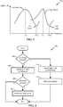
- FIG. 3 shows a frequency plot 300 that illustrates amplification over the wide frequency range (i.e., 800MHz-2.4GHz) of the DA output of the driver amplifier 106.
- the plot 300 shows amplification over the low frequency band having a tunable fundamental frequency ( f LB ). Operation in the low frequency band is determined from operation of the first (or low) band selection circuit 238.
- the plot 300 also shows the 2 nd harmonic attenuation (LB notch) at the 2 nd harmonic of the low band frequency (2 f LB ) provided by the LB trap circuit 230.
- LB notch 2 nd harmonic attenuation
- the plot 300 also shows amplification over the high frequency band having a tunable fundamental frequency ( f HB ). Operation in the high frequency band is determined from operation of the second (or high) band selection circuit 220.
- the plot 300 shows the 2 nd harmonic attenuation (HB notch) at the 2 nd harmonic of the high band frequency (2 f HB ) provided by the high band 2 nd harmonic trap circuit 214.
- FIG. 4 shows an exemplary embodiment of a method 400 for wide band amplification in a wireless device.
- the method 400 is suitable for use with the driver amplifier 106 shown in FIG. 2 .
- the HB enable signal 228 is set to the disabled state so that the transistor 226 is disabled thereby de-coupling the capacitor 224 from the circuit ground.
- the low band selection circuit 238 comprising the inductor L LOW 210 and capacitor 212 sets the tunable center frequency ( f LB ) for amplification in the low band.
- the inductor L LOW 210 and the variable capacitor 212 are configured to tune the center frequency ( f LB ) of the first (low) frequency band from 800MHz to 1.4GHz.
- the base band processor 102 outputs the LB trap enable signal 236 that is used to determine if the low band notch filter is to be enabled. If the LB trap enable signal 236 is disabled, then the low band notch filter is disabled and the method ends. If the LB trap enable signal 236 is enabled, then the low band notch filter is to be enabled and the method proceeds to block 408.
- the low band notch is enabled.
- the LB trap enable signal 236 operates to enable the low band trap circuit 230 so that the transistor 234 couples the capacitor 232 to the circuit ground.
- the combination of the inductor L HIGH 222 and the capacitor 232 operate to provide a low band trap to reduce or attenuate frequencies at and above the low band 2 nd harmonic frequency (2 f LB ) .
- high band amplification is enabled.
- the HB enable signal 228 is set to the enabled state so that the transistor 226 is enabled thereby coupling the capacitor 224 to the circuit ground.
- the second band selection circuit 220 is enabled.
- the LB trap circuit 230 is enabled by the LB trap enable signal 236.
- the combination of the inductor L HIGH 222, capacitor 224 and capacitor 232 operates to push or adjust the amplification band of the amplifier 106 to the high band.
- the center frequency is tuned to ( f HB ) to provide amplification in the high band.
- the high band notch filter is enabled.
- the tank circuit 214 comprising the combination of the inductor 218 and the capacitor 216 operate to provide a high band trap to reduce or attenuate frequencies at and above the high band 2 nd harmonic frequency (2 f HB ) .
- the method 400 provides for wide band amplification in a wireless device that reduces the required die area over conventional amplifiers. It should be noted that the operations of the method 400 can be rearranged, modified or changed by one with skill in the art such that other equivalent methods are possible.
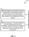
- FIG. 5 shows an exemplary embodiment of a wide band driver amplifier apparatus 500.
- the apparatus 500 is suitable for use with the driver amplifier 106 shown in FIG. 2 .
- the apparatus 500 is implemented by one or more modules configured to provide the functions as described herein.
- each module comprises hardware and/or hardware executing software.
- the apparatus 500 comprises a first module comprising means ( 502 ) for adjusting an amplification band of an amplifier from a first frequency band to a second frequency band, the means for adjusting selectively connected between an output terminal of the amplifier and a circuit ground, which in an aspect comprises the second band selection circuit 220.
- the apparatus 500 comprises a second module comprising means ( 504 ) for reducing 2 nd harmonic frequencies in the first frequency band when the amplification band is set to the first frequency band, the means for reducing connected between the means for adjusting and the circuit ground, which in an aspect comprises the first harmonic reduction circuit 230.
- transistor types and technologies may be substituted, rearranged or otherwise modified to achieve the same results.
- circuits shown utilizing PMOS transistors may be modified to use NMOS transistors and vice versa.
- the amplifiers disclosed herein may be realized using a variety of transistor types and technologies and are not limited to those transistor types and technologies illustrated in the Drawings.
- transistors types such as BJT, GaAs, MOSFET or any other transistor technology may be used.
- DSP Digital Signal Processor
- ASIC Application Specific Integrated Circuit
- FPGA Field Programmable Gate Array
- a general purpose processor may be a microprocessor, but in the alternative, the processor may be any conventional processor, controller, microcontroller, or state machine.
- a processor may also be implemented as a combination of computing devices, e.g., a combination of a DSP and a microprocessor, a plurality of microprocessors, one or more microprocessors in conjunction with a DSP core, or any other such configuration.
- a software module may reside in Random Access Memory (RAM), flash memory, Read Only Memory (ROM), Electrically Programmable ROM (EPROM), Electrically Erasable Programmable ROM (EEPROM), registers, hard disk, a removable disk, a CD-ROM, or any other form of storage medium known in the art.
- An exemplary storage medium is coupled to the processor such that the processor can read information from, and write information to, the storage medium.
- the storage medium may be integral to the processor.
- the processor and the storage medium may reside in an ASIC.
- the ASIC may reside in a user terminal.
- the processor and the storage medium may reside as discrete components in a user terminal.
- the functions described may be implemented in hardware, software, firmware, or any combination thereof. If implemented in software, the functions may be stored on or transmitted over as one or more instructions or code on a computer-readable medium.
- Computer-readable media includes both non-transitory computer storage media and communication media including any medium that facilitates transfer of a computer program from one place to another.
- a non-transitory storage media may be any available media that can be accessed by a computer.
- such computer-readable media can comprise RAM, ROM, EEPROM, CD-ROM or other optical disk storage, magnetic disk storage or other magnetic storage devices, or any other medium that can be used to carry or store desired program code in the form of instructions or data structures and that can be accessed by a computer.
- any connection is properly termed a computer-readable medium.
- the software is transmitted from a website, server, or other remote source using a coaxial cable, fiber optic cable, twisted pair, digital subscriber line (DSL), or wireless technologies such as infrared, radio, and microwave
- the coaxial cable, fiber optic cable, twisted pair, DSL, or wireless technologies such as infrared, radio, and microwave are included in the definition of medium.
- Disk and disc includes compact disc (CD), laser disc, optical disc, digital versatile disc (DVD), floppy disk and blu-ray disc where disks usually reproduce data magnetically, while discs reproduce data optically with lasers. Combinations of the above should also be included within the scope of computer-readable media.
Landscapes
- Engineering & Computer Science (AREA)
- Power Engineering (AREA)
- Amplifiers (AREA)
Description
- This patent application claims the benefit of priority from
U.S. Provisional Patent Application No. 61/738,251 - The present application relates generally to the operation and design of analog front ends, and more particularly, to the operation and design of driver amplifiers for use in analog front ends.
- Wireless devices have become increasingly more complex resulting in more circuitry being incorporated onto smaller chips and circuit boards. For example, a conventional transmitter used in a wireless device may include multiple driver amplifiers (DA) to amplify signals in both low frequency and high frequency bands, respectively. Having a dedicated DA for a specified frequency band may achieve the desired amplification goals; however such an implementation also may have several disadvantages. For example, utilizing multiple DAs may result in increased costs in terms of die area requirements. Furthermore, other circuitry in the transmitter, such as an up-converter, may need to be modified to support multiple DA configurations, thereby increasing the complexity of the transmitter.
- Accordingly, what is needed is a highly efficient wide band driver amplifier that is configured to reduce die area and transmitter design complexity in wireless devices.
Attention is drawn toUS2008/0290947 describing a multi-band, multi-standard programmable power amplifier having tunable impedance matching input and output networks and programmable device characteristics. The impedance of either or both of the impedance matching input and output networks is tunable responsive to one or more control signals. In one example, the programmable power amplifier incorporates a feedback control loop and the control signals are varied responsive to the feedback loop. - Further attention is drawn to
US 2012/087282 A1 describing a wireless communication high-frequency circuit in which a broadband amplifier is shared between multiple communication frequency bands and multiple duplexers are used in order to support the multiple communication frequency bands including a first impedance matching circuit between an output port of an amplifier and a relay switch. A first signal path extends from the output port of the amplifier to the ground in the first impedance matching circuit. An inductor and a variable capacitance element are provided on the first signal path. Second impedance matching circuits are provided between output ports and the input port of the relay switch and transmission signal input ports of duplexers, respectively. - Further attention is drawn to
US 6 023 611 A describing a power amplifier device, switchable for at least two separate basic frequency bands, for radio frequency signals with suppression of harmonics, where harmonics, corresponding to a first basic frequency band, can be permitted to overlap the frequency range of at least one second basic frequency band. The power amplifier device comprises a power amplifier and an impedance matching circuit, switchable by means of a PIN-diode, which provides a load impedance adapted to each individual basic frequency band. Furthermore, the power amplifier device comprises a filter device comprising a fixed low-pass filter and a switchable filter acting as an engageable and disengageable notch filter, which comprises at least one reversible PIN-diode. This switchable filter allows to pass, in a first mode, signals in the first basic frequency band and suppresses at the same time at least one order of harmonics corresponding to this basic frequency band. In a second mode, the second basic frequency band is transmitted, and harmonics are suppressed by the fixed low-pass filter.
In accordance with the present invention an apparatus and a method, as set forth in the independent claims, is provided. Embodiments of the invention are claimed in the dependent claims. - The foregoing aspects described herein will become more readily apparent by reference to the following description when taken in conjunction with the accompanying drawings wherein:
-
FIG. 1 shows a transmitter for use in a device that includes an exemplary embodiment of a tunable wide band driver amplifier; -
FIG. 2 shows a detailed exemplary embodiment of the tunable wide band driver amplifier illustrated inFIG. 1 ; -
FIG. 3 shows a frequency plot that illustrates the wide band frequency range of the output of the driver amplifier shown inFIG. 2 ; -
FIG. 4 shows an exemplary embodiment of a method for wide band amplification in a wireless device; and -
FIG. 5 shows an exemplary embodiment of a tunable wide band driver amplifier apparatus. -
FIG. 1 shows atransmitter 100 for use in a device that includes an exemplary embodiment of a novel tunable wide band DA 106. Thetransmitter 100 comprises abaseband processor 102 that outputs baseband data to be transmitted to an up-converter 104. The up-converter 104 up-converts the baseband data to a radio frequency (RF) signal and inputs this RF signal to the tunablewide band DA 106. Thetunable DA 106 is configured to provide amplification over a wide frequency range (i.e., 800Mhz to 2.4GHz) that is divided into two selectable frequency bands. Thetunable DA 106 receives a bandselect signal 110 from thebaseband processor 102. The band selectsignal 110 selects one of the two selectable bands over which amplification will be provided. Thetunable DA 106 also receives a trap enablesignal 112 from thebaseband processor 102. The trap enablesignal 112 enables or disables a trap circuit that provides attenuation of 2nd harmonic and higher frequencies for the amplified output. The amplified output of thetunable DA 106 is then input to a power amplifier (PA) 108 where the RF signal is further amplified for transmission. In various exemplary embodiments, thetunable DA 106 provides amplification over a wide frequency range and is configured to reduce die area by half when compared to conventional DA configurations that utilize multiple amplifiers. -
FIG. 2 shows a detailed exemplary embodiment of the tunable wideband driver amplifier 106 illustrated inFIG. 1 . Theupconverter 104 outputs a differential signal to abalun 202 that converts the differential signal to a single-ended signal. The single-ended signal is input totransistor 204 of theDA 106. Thetransistor 204 operates withtransistor 206 to amplify the single-ended signal to generate an amplified output signal (DA output) at thedrain terminal 208 oftransistor 206. It should be noted that although thetransistors amplifier 106 may utilize any suitable transistor configuration. - In an exemplary embodiment, a first
band selection circuit 238 operates to set the amplification band of the amplifier to a first frequency band. The first frequency band (also referred to herein as the low frequency band) has a center frequency designated as (fLB ). The firstband selection circuit 238 comprises aninductor L LOW 210 andvariable capacitor 212. Theinductor L LOW 210 is connected between thedrain terminal 208 and a supply voltage (VDD). Thevariable capacitor 212 is connected between thedrain terminal 208 and a circuit ground. In an exemplary embodiment, theinductor L LOW 210 has a large inductance value (i.e., 4nH) and thevariable capacitor 212 has a tunable capacitance range (i.e., 1-10pf). Theinductor L LOW 210 and thevariable capacitor 212 combine to set the first frequency band of operation for theDA 106. In an exemplary embodiment, theinductor L LOW 210 and thevariable capacitor 212 are configured to tune the center frequency (fLB ) of the first frequency band from 800MHz to 1.4GHz. - A low
band trap circuit 230 operates to provide 2nd harmonic frequency reduction for the amplified DA output signal when operating in the first frequency band of operation. The lowband trap circuit 230 comprises avariable capacitor 232 connected between aninductor L HIGH 222 and a drain terminal oftransistor 234. Theinductor L HIGH 222 also is connected to thedrain terminal 208. In an exemplary embodiment, thecapacitor 232 has a tunable capacitance value in the range of 1-6pf and theinductor L HIGH 222 has an inductance value of 2nH. Thetransistor 234 has a source terminal connected to the circuit ground and a gate terminal that is controlled by a low band (LB) trap enablesignal 236. For example, when the LB trap enablesignal 236 is in a "high voltage" or "enable" state, thetransistor 234 is turned on so that thecapacitor 232 is coupled to the circuit ground. When the LB trap enablesignal 236 is in a "low voltage" or "disable" state, thetransistor 234 is turned off so that thecapacitor 232 is de-coupled from the circuit ground. In an exemplary embodiment, the trap enablesignal 112 illustrated inFIG. 1 comprises the LB trap enablesignal 236 and is generated by thebaseband processor 102 or some other entity at the device. - When the LB trap enable
signal 236 enables (or turns on) thetransistor 234 so that thecapacitor 232 is coupled to the circuit ground, the combination of theinductor L HIGH 222 and thecapacitor 232 operate to form a low band trap circuit to provide 2nd harmonic frequency reduction for the amplified DA output signal when in the low frequency band of operation. For example, when the lowband trap circuit 230 is enabled, DA output frequencies at and above the 2nd harmonic frequency (2fLB ) of the low band center frequency (fLB ) are reduced or attenuated. - In an exemplary embodiment, a second
band selection circuit 220 operates to set the amplification band of theDA 106 to a second frequency band. The second frequency band (also is referred to herein as the high frequency band) has a center frequency designated as (fHB ). The secondband selection circuit 220 includes the lowband trap circuit 230. In an exemplary embodiment, the secondband selection circuit 220 also comprises theinductor L HIGH 222 connected in series with acapacitor 224. For example, in an exemplary embodiment, thecapacitor 224 has a fixed capacitance value of 10pf. Thecapacitor 224 is further connected to a drain terminal oftransistor 226, which also has a source terminal connected to the circuit ground. Thetransistor 226 has a gate terminal that is connected to and controlled by a high band (HB) enablesignal 228. For example, when the HB enablesignal 228 is in a "high voltage" or "enable" state, thetransistor 226 is turned on so that thecapacitor 224 is coupled to the circuit ground. When the HB enablesignal 228 is in a "low voltage" or "disable" state, thetransistor 226 is turned off so that thecapacitor 224 is de-coupled from the circuit ground. In an exemplary embodiment, the bandselect signal 110 illustrated inFIG. 1 comprises the HB enablesignal 228 and is generated by thebaseband processor 102 or some other entity at the device. - In an exemplary embodiment, when both the HB enable
signal 228 and the LB trap enablesignal 236 are set to the enabled state, thetransistors capacitors capacitors capacitor 232. This combined capacitance in combination with theinductor L HIGH 222, theinductor L LOW 210, and thecapacitor 212 operate to adjust the amplification band of theDA 106 to the second (or high) frequency band. In an exemplary embodiment, the secondband selection circuit 220 is configured to tune the center frequency (fHB ) of the second frequency band from 1.4GHz to 2.4GHz. - A
tank circuit 214 comprisingtunable capacitor 216 andinductor 218 is connected between asource terminal 240 of thetransistor 204 and the circuit ground. Thetank circuit 214 operates to provide 2nd harmonic reduction when the amplification band of theDA 106 is set to the second (or high) frequency band. In an exemplary embodiment, theinductor 218 has an inductance value of .25nH and thetunable capacitor 216 has a capacitance value in the range of .5-4pf. For example, thetank circuit 214 operates so that DA output frequencies at and above a 2nd harmonic (2fHB ) of the high band center frequency (fHB ) are reduced or attenuated. For example, thetank circuit 214 presents a high impedance at high order harmonic frequencies of the high band (i.e., 2nd harmonic (2fHB ) and higher frequencies) to suppress the generation of such frequencies. At the fundamental frequency (fHB ), thetank 214 will show considerably lower impedance and have minor impact to the gain of the common source stage. Furthermore, at the low frequency band, theinductor 218 will have little effect and thetunable capacitor 216 can be disabled or turned off. - In various exemplary embodiments, the values of the
inductors L LOW 210,L HIGH 222 andvariable capacitors inductors L LOW 210 andL HIGH 222 are determined at manufacture and the values of thevariable capacitors base band processor 102. For example, in an exemplary embodiment, the bandselect signal 110 that is output from thebase band processor 102 comprises control signals (not shown inFIG. 2 ) that enable, disable and select the capacitance values of thevariable capacitors - During operation of the
wide band DA 106, the enable signals 228 and 236 are used to set the amplification band of theDA 106 to either the first (low) or second (high) frequency bands. For each frequency band, 2nd harmonic reduction is automatically enabled or can be selectively enabled to reduce or attenuate output frequencies at and above the 2nd harmonic frequency of the selected band's center frequency. A more detailed description of the operation of the wideband driver amplifier 106 is provided below. -
FIG. 3 shows afrequency plot 300 that illustrates amplification over the wide frequency range (i.e., 800MHz-2.4GHz) of the DA output of thedriver amplifier 106. Theplot 300 shows amplification over the low frequency band having a tunable fundamental frequency (fLB ). Operation in the low frequency band is determined from operation of the first (or low)band selection circuit 238. Theplot 300 also shows the 2nd harmonic attenuation (LB notch) at the 2nd harmonic of the low band frequency (2fLB ) provided by theLB trap circuit 230. - The
plot 300 also shows amplification over the high frequency band having a tunable fundamental frequency (fHB ). Operation in the high frequency band is determined from operation of the second (or high)band selection circuit 220. Theplot 300 shows the 2nd harmonic attenuation (HB notch) at the 2nd harmonic of the high band frequency (2fHB ) provided by the high band 2ndharmonic trap circuit 214. -
FIG. 4 shows an exemplary embodiment of amethod 400 for wide band amplification in a wireless device. For example, themethod 400 is suitable for use with thedriver amplifier 106 shown inFIG. 2 . - At
block 402, a determination is made to determine whether amplification in a low frequency band is selected. For example, thebase band processor 102 outputs the HB enablesignal 228 to set the amplification band. If the HB enablesignal 228 is disabled, then amplification in the low frequency band is selected. If the HB enablesignal 228 is enabled, then amplification in the high frequency band is selected. If amplification in the low frequency band is selected, the method proceeds to block 404. If amplification in the high frequency band is selected, the method proceeds to block 410. - At
block 404, amplification in the low band is enabled. In an exemplary embodiment, the HB enablesignal 228 is set to the disabled state so that thetransistor 226 is disabled thereby de-coupling thecapacitor 224 from the circuit ground. As a result, the lowband selection circuit 238 comprising theinductor L LOW 210 andcapacitor 212 sets the tunable center frequency (fLB ) for amplification in the low band. In an exemplary embodiment, theinductor L LOW 210 and thevariable capacitor 212 are configured to tune the center frequency (fLB ) of the first (low) frequency band from 800MHz to 1.4GHz. - At
block 406, a determination is made as to whether a low band notch filter is to be enabled. For example, thebase band processor 102 outputs the LB trap enablesignal 236 that is used to determine if the low band notch filter is to be enabled. If the LB trap enablesignal 236 is disabled, then the low band notch filter is disabled and the method ends. If the LB trap enablesignal 236 is enabled, then the low band notch filter is to be enabled and the method proceeds to block 408. - At
block 408, the low band notch is enabled. In an exemplary embodiment, the LB trap enablesignal 236 operates to enable the lowband trap circuit 230 so that thetransistor 234 couples thecapacitor 232 to the circuit ground. The combination of theinductor L HIGH 222 and thecapacitor 232 operate to provide a low band trap to reduce or attenuate frequencies at and above the low band 2nd harmonic frequency (2fLB ). - At
block 410, high band amplification is enabled. In an exemplary embodiment, the HB enablesignal 228 is set to the enabled state so that thetransistor 226 is enabled thereby coupling thecapacitor 224 to the circuit ground. As a result, the secondband selection circuit 220 is enabled. Additionally, theLB trap circuit 230 is enabled by the LB trap enablesignal 236. The combination of theinductor L HIGH 222,capacitor 224 andcapacitor 232 operates to push or adjust the amplification band of theamplifier 106 to the high band. For example, the center frequency is tuned to (fHB ) to provide amplification in the high band. - At
block 412, the high band notch filter is enabled. In an exemplary embodiment, thetank circuit 214 comprising the combination of theinductor 218 and thecapacitor 216 operate to provide a high band trap to reduce or attenuate frequencies at and above the high band 2nd harmonic frequency (2fHB ). - Accordingly, the
method 400 provides for wide band amplification in a wireless device that reduces the required die area over conventional amplifiers. It should be noted that the operations of themethod 400 can be rearranged, modified or changed by one with skill in the art such that other equivalent methods are possible. -
FIG. 5 shows an exemplary embodiment of a wide banddriver amplifier apparatus 500. For example, theapparatus 500 is suitable for use with thedriver amplifier 106 shown inFIG. 2 . In an aspect, theapparatus 500 is implemented by one or more modules configured to provide the functions as described herein. For example, in an aspect, each module comprises hardware and/or hardware executing software. - The
apparatus 500 comprises a first module comprising means (502) for adjusting an amplification band of an amplifier from a first frequency band to a second frequency band, the means for adjusting selectively connected between an output terminal of the amplifier and a circuit ground, which in an aspect comprises the secondband selection circuit 220. - The
apparatus 500 comprises a second module comprising means (504) for reducing 2nd harmonic frequencies in the first frequency band when the amplification band is set to the first frequency band, the means for reducing connected between the means for adjusting and the circuit ground, which in an aspect comprises the firstharmonic reduction circuit 230. - Those of skill in the art would understand that information and signals may be represented or processed using any of a variety of different technologies and techniques. For example, data, instructions, commands, information, signals, bits, symbols, and chips that may be referenced throughout the above description may be represented by voltages, currents, electromagnetic waves, magnetic fields or particles, optical fields or particles, or any combination thereof. It is further noted that transistor types and technologies may be substituted, rearranged or otherwise modified to achieve the same results. For example, circuits shown utilizing PMOS transistors may be modified to use NMOS transistors and vice versa. Thus, the amplifiers disclosed herein may be realized using a variety of transistor types and technologies and are not limited to those transistor types and technologies illustrated in the Drawings. For example, transistors types such as BJT, GaAs, MOSFET or any other transistor technology may be used.
- Those of skill would further appreciate that the various illustrative logical blocks, modules, circuits, and algorithm steps described in connection with the embodiments disclosed herein may be implemented as electronic hardware, computer software, or combinations of both. To clearly illustrate this interchangeability of hardware and software, various illustrative components, blocks, modules, circuits, and steps have been described above generally in terms of their functionality. Whether such functionality is implemented as hardware or software depends upon the particular application and design constraints imposed on the overall system. Skilled artisans may implement the described functionality in varying ways for each particular application, but such implementation decisions should not be interpreted as causing a departure from the scope of the exemplary embodiments of the invention.
- The various illustrative logical blocks, modules, and circuits described in connection with the embodiments disclosed herein may be implemented or performed with a general purpose processor, a Digital Signal Processor (DSP), an Application Specific Integrated Circuit (ASIC), a Field Programmable Gate Array (FPGA) or other programmable logic device, discrete gate or transistor logic, discrete hardware components, or any combination thereof designed to perform the functions described herein. A general purpose processor may be a microprocessor, but in the alternative, the processor may be any conventional processor, controller, microcontroller, or state machine. A processor may also be implemented as a combination of computing devices, e.g., a combination of a DSP and a microprocessor, a plurality of microprocessors, one or more microprocessors in conjunction with a DSP core, or any other such configuration.
- The steps of a method or algorithm described in connection with the embodiments disclosed herein may be embodied directly in hardware, in a software module executed by a processor, or in a combination of the two. A software module may reside in Random Access Memory (RAM), flash memory, Read Only Memory (ROM), Electrically Programmable ROM (EPROM), Electrically Erasable Programmable ROM (EEPROM), registers, hard disk, a removable disk, a CD-ROM, or any other form of storage medium known in the art. An exemplary storage medium is coupled to the processor such that the processor can read information from, and write information to, the storage medium. In the alternative, the storage medium may be integral to the processor. The processor and the storage medium may reside in an ASIC. The ASIC may reside in a user terminal. In the alternative, the processor and the storage medium may reside as discrete components in a user terminal.
- In one or more exemplary embodiments, the functions described may be implemented in hardware, software, firmware, or any combination thereof. If implemented in software, the functions may be stored on or transmitted over as one or more instructions or code on a computer-readable medium. Computer-readable media includes both non-transitory computer storage media and communication media including any medium that facilitates transfer of a computer program from one place to another. A non-transitory storage media may be any available media that can be accessed by a computer. By way of example, and not limitation, such computer-readable media can comprise RAM, ROM, EEPROM, CD-ROM or other optical disk storage, magnetic disk storage or other magnetic storage devices, or any other medium that can be used to carry or store desired program code in the form of instructions or data structures and that can be accessed by a computer. Also, any connection is properly termed a computer-readable medium. For example, if the software is transmitted from a website, server, or other remote source using a coaxial cable, fiber optic cable, twisted pair, digital subscriber line (DSL), or wireless technologies such as infrared, radio, and microwave, then the coaxial cable, fiber optic cable, twisted pair, DSL, or wireless technologies such as infrared, radio, and microwave are included in the definition of medium. Disk and disc, as used herein, includes compact disc (CD), laser disc, optical disc, digital versatile disc (DVD), floppy disk and blu-ray disc where disks usually reproduce data magnetically, while discs reproduce data optically with lasers. Combinations of the above should also be included within the scope of computer-readable media.
- The description of the disclosed exemplary embodiments is provided to enable any person skilled in the art to make or use the invention. Various modifications to these exemplary embodiments will be readily apparent to those skilled in the art, and the generic principles defined herein may be applied to other embodiments without departing from the scope of the invention. Thus, the invention is not intended to be limited to the exemplary embodiments shown herein but is to be accorded the widest scope consistent with the principles and novel features disclosed herein.
Claims (12)
- An apparatus (106), comprising:means (220) configured to adjust an amplification band of an amplifier from a first low frequency band to a second high frequency band, the means (220) configured to adjust selectively connected between an output terminal (208) of the amplifier and a circuit ground;means (238) configured to set the amplification band of the amplifier to the first low frequency band, the means (238) configured to set includes means configured to provide a variable capacitance (212) connected directly between the output terminal (208) and the circuit ground, wherein the means (220) configured to adjust and the means (238) configured to set are connected in parallel; andwherein the means (220) configured to adjust comprises means (230) configured to reduce 2nd harmonic frequencies in the first low frequency band when the amplification band is set to the first low frequency band, the means configured to adjust and the means configured to reduce share a common inductor (222).
- The apparatus (106) of claim 1, wherein said means (238) configured to set the amplification band of the amplifier to the first low frequency band comprises:
a first inductor (210) connected between the output terminal (208) and a supply voltage. - The apparatus (106) of claim 1, the means configured to adjust (220) comprising:said common inductor being a first inductor (222) connected to the output terminal (208);a first capacitor (224) connect to the first inductor (222); anda switch (226) configured to selectively connect the first capacitor (224) to the circuit ground to set the amplification band to the second high frequency band.
- The apparatus (106) of claim 3, the means (230) configured to reduce comprising:a second capacitor (232) connected to the first inductor (222); anda switch (234) configured to selectively connect the second capacitor (232) to the circuit ground to enable reduction of the 2nd harmonic frequencies in the first low frequency band when the amplification band is set to the first low frequency band and to tune the center frequency of the second high frequency band when the amplification band is set to the second high frequency band.
- The apparatus (106) of claim 1, the amplifier comprising first and second transistors (206, 204) and the output terminal (208) connected to a drain terminal of the first transistor (206).
- The apparatus (106) of claim 5, further comprising means (214) configured to trap connected to a source terminal of the second transistor (204) and configured to reduce 2nd harmonic frequencies when the amplification band is set to the second high frequency band.
- The apparatus of claim 6, the means (214) configured to trap comprising:an inductor (218) connected between the source terminal of the second transistor (204) and the circuit ground; anda capacitor (216) connected between the source terminal of the second transistor (204) and the circuit ground.
- The apparatus of claim 1, the first low frequency band having a first center frequency that is lower in frequency than a second center frequency of the second high frequency band.
- A method (400) comprising:determining (402) whether an amplification band of an amplifier is to be set to a low frequency band or a high frequency band;enabling (404) a first band selection circuit (238) having a variable capacitor (212) connected directly between an output terminal (208) of the amplifier and a circuit ground and disabling a second band selection circuit (220) selectively connected between the output terminal of the amplifier and the circuit ground if the amplification band is to be set to the low frequency band, wherein first band selection circuit (238) and the second band selection circuit (220) are connected in parallel;enabling (410) the first band selection circuit (238) and enabling the second band selection circuit (220) if the amplification band is to be set to the high frequency band; and enabling a low band trap circuit (230), if the amplification band is to be set to the low frequency band, the second band selection circuit (220) and the low band trap circuit (230) share a common inductor (222).
- The method (400) of claim 9, further comprising:determining (406) whether the low band trap circuit (230) is to be enabled if the amplification band is to be set to the low frequency band;enabling (408) the low band trap circuit (230) to reduce 2nd harmonic frequencies associated with the low frequency band if the low band trap circuit (230) is to be enabled.
- The method (400) of claim 9, further comprising enabling (412) a high band trap circuit (214) to reduce 2nd harmonic frequencies associated with the high frequency band if the amplification band is to be set to the high frequency band.
- The method (400) of claim 9, the low frequency band having a first center frequency that is lower in frequency than a second center frequency of the high frequency band.
Applications Claiming Priority (3)
| Application Number | Priority Date | Filing Date | Title |
|---|---|---|---|
| US201261738251P | 2012-12-17 | 2012-12-17 | |
| US13/775,026 US9035703B2 (en) | 2012-12-17 | 2013-02-22 | Tunable wide band driver amplifier |
| PCT/US2013/075880 WO2014100046A1 (en) | 2012-12-17 | 2013-12-17 | Tunable wide band driver amplifier |
Publications (2)
| Publication Number | Publication Date |
|---|---|
| EP2932594A1 EP2932594A1 (en) | 2015-10-21 |
| EP2932594B1 true EP2932594B1 (en) | 2019-07-03 |
Family
ID=50930200
Family Applications (1)
| Application Number | Title | Priority Date | Filing Date |
|---|---|---|---|
| EP13818898.2A Active EP2932594B1 (en) | 2012-12-17 | 2013-12-17 | Tunable wide band driver amplifier |
Country Status (5)
| Country | Link |
|---|---|
| US (1) | US9035703B2 (en) |
| EP (1) | EP2932594B1 (en) |
| JP (1) | JP6030248B2 (en) |
| CN (1) | CN104871429B (en) |
| WO (1) | WO2014100046A1 (en) |
Families Citing this family (10)
| Publication number | Priority date | Publication date | Assignee | Title |
|---|---|---|---|---|
| US8949455B2 (en) | 2005-11-21 | 2015-02-03 | Oracle International Corporation | Path-caching mechanism to improve performance of path-related operations in a repository |
| US9673853B2 (en) * | 2014-08-21 | 2017-06-06 | Skyworks Solutions, Inc. | Cascode power amplifier with voltage limiter |
| US9589916B2 (en) * | 2015-02-10 | 2017-03-07 | Infineon Technologies Ag | Inductively coupled transformer with tunable impedance match network |
| US10187023B2 (en) * | 2015-02-15 | 2019-01-22 | Skyworks Solutions, Inc. | Power amplifier with cascode switching or splitting functionality |
| US20160301369A1 (en) * | 2015-04-10 | 2016-10-13 | Ferfics Limited | Band optimised rf switch low noise amplifier |
| US9941849B1 (en) * | 2017-02-10 | 2018-04-10 | Psemi Corporation | Programmable optimized band switching LNA for operation in multiple narrow-band frequency ranges |
| US11881828B2 (en) | 2017-04-04 | 2024-01-23 | Psemi Corporation | Tunable effective inductance for multi-gain LNA with inductive source degeneration |
| US10038418B1 (en) | 2017-04-04 | 2018-07-31 | Psemi Corporation | Optimized multi gain LNA enabling low current and high linearity including highly linear active bypass |
| US10601376B2 (en) * | 2018-03-19 | 2020-03-24 | Psemi Corporation | Input third order intercept point in low noise amplifier with degeneration tank circuit |
| KR20240107462A (en) * | 2022-12-30 | 2024-07-09 | 충남대학교산학협력단 | Amplifier |
Family Cites Families (20)
| Publication number | Priority date | Publication date | Assignee | Title |
|---|---|---|---|---|
| JPH07263980A (en) * | 1994-03-18 | 1995-10-13 | Matsushita Electric Ind Co Ltd | Semiconductor device |
| JP3039749B2 (en) * | 1994-03-18 | 2000-05-08 | 株式会社富士通ゼネラル | Parabolic antenna device |
| JP3160525B2 (en) * | 1996-03-26 | 2001-04-25 | 株式会社ヨコオ | Transistor amplifier circuit |
| SE508506C2 (en) | 1997-02-25 | 1998-10-12 | Ericsson Telefon Ab L M | Device and method of telecommunication |
| JP3811557B2 (en) | 1997-10-21 | 2006-08-23 | 松下電器産業株式会社 | Multiple frequency band high efficiency linear power amplifier |
| US7202734B1 (en) * | 1999-07-06 | 2007-04-10 | Frederick Herbert Raab | Electronically tuned power amplifier |
| US6650185B1 (en) | 2002-04-26 | 2003-11-18 | Motorola, Inc | Frequency selective distributed amplifier |
| US6806767B2 (en) * | 2002-07-09 | 2004-10-19 | Anadigics, Inc. | Power amplifier with load switching circuit |
| US7173505B2 (en) | 2003-10-23 | 2007-02-06 | Broadcom Corporation | Tuning RF circuits using switched inductors provided in a monolithic integrated circuit |
| JP2007110685A (en) * | 2005-09-16 | 2007-04-26 | Oki Electric Ind Co Ltd | Receiver and method of attenuating disturbance signal |
| JPWO2007099622A1 (en) * | 2006-03-01 | 2009-07-16 | 富士通株式会社 | Amplifier circuit |
| JP4485487B2 (en) | 2006-05-11 | 2010-06-23 | シャープ株式会社 | Power amplifier |
| KR20080007861A (en) * | 2006-07-18 | 2008-01-23 | (주)네오팜 | Novel microorganisms having biodegradation ability for oil and bioremediation method for oil-contaminated sites |
| US7949322B2 (en) | 2007-03-09 | 2011-05-24 | Qualcomm, Incorporated | Frequency selective amplifier with wide-band impedance and noise matching |
| WO2008136080A1 (en) * | 2007-04-20 | 2008-11-13 | Fujitsu Limited | Amplifier apparatus |
| WO2008147932A2 (en) | 2007-05-24 | 2008-12-04 | Bitwave Semiconductor, Incorporated | Reconfigurable tunable rf power amplifier |
| US8228123B2 (en) | 2007-08-29 | 2012-07-24 | Nxp B.V. | Integrated Doherty amplifier |
| US9143172B2 (en) * | 2009-06-03 | 2015-09-22 | Qualcomm Incorporated | Tunable matching circuits for power amplifiers |
| WO2011001769A1 (en) | 2009-07-02 | 2011-01-06 | 株式会社村田製作所 | High-frequency circuit for radio communication, and radio communication device |
| US8629725B2 (en) * | 2010-12-05 | 2014-01-14 | Rf Micro Devices (Cayman Islands), Ltd. | Power amplifier having a nonlinear output capacitance equalization |
-
2013
- 2013-02-22 US US13/775,026 patent/US9035703B2/en active Active
- 2013-12-17 WO PCT/US2013/075880 patent/WO2014100046A1/en active Application Filing
- 2013-12-17 EP EP13818898.2A patent/EP2932594B1/en active Active
- 2013-12-17 JP JP2015548059A patent/JP6030248B2/en active Active
- 2013-12-17 CN CN201380065858.XA patent/CN104871429B/en active Active
Non-Patent Citations (1)
| Title |
|---|
| None * |
Also Published As
| Publication number | Publication date |
|---|---|
| WO2014100046A1 (en) | 2014-06-26 |
| US20140167864A1 (en) | 2014-06-19 |
| US9035703B2 (en) | 2015-05-19 |
| CN104871429B (en) | 2018-01-12 |
| CN104871429A (en) | 2015-08-26 |
| JP6030248B2 (en) | 2016-11-24 |
| JP2016500499A (en) | 2016-01-12 |
| EP2932594A1 (en) | 2015-10-21 |
Similar Documents
| Publication | Publication Date | Title |
|---|---|---|
| EP2932594B1 (en) | Tunable wide band driver amplifier | |
| US8031005B2 (en) | Amplifier supporting multiple gain modes | |
| US8842410B2 (en) | Switchable inductor network | |
| KR101983632B1 (en) | Communication module | |
| EP2883275B1 (en) | Front end parallel resonant switch | |
| US20150042412A1 (en) | Directional coupler circuit techniques | |
| EP2946467B1 (en) | Amplifier with switchable common gate gain buffer | |
| US9312927B2 (en) | Tunable guard ring for improved circuit isolation | |
| EP2707948A2 (en) | System providing switchable impedance transformer matching for power amplifiers | |
| EP3084958B1 (en) | Tunable loadline | |
| US9026060B2 (en) | Bidirectional matching network | |
| WO2015031199A1 (en) | Combination nmos/pmos power amplifier | |
| EP2792067A1 (en) | Millimeter wave power amplifier |
Legal Events
| Date | Code | Title | Description |
|---|---|---|---|
| PUAI | Public reference made under article 153(3) epc to a published international application that has entered the european phase |
Free format text: ORIGINAL CODE: 0009012 |
|
| 17P | Request for examination filed |
Effective date: 20150713 |
|
| AK | Designated contracting states |
Kind code of ref document: A1 Designated state(s): AL AT BE BG CH CY CZ DE DK EE ES FI FR GB GR HR HU IE IS IT LI LT LU LV MC MK MT NL NO PL PT RO RS SE SI SK SM TR |
|
| AX | Request for extension of the european patent |
Extension state: BA ME |
|
| DAX | Request for extension of the european patent (deleted) | ||
| STAA | Information on the status of an ep patent application or granted ep patent |
Free format text: STATUS: EXAMINATION IS IN PROGRESS |
|
| 17Q | First examination report despatched |
Effective date: 20170303 |
|
| GRAP | Despatch of communication of intention to grant a patent |
Free format text: ORIGINAL CODE: EPIDOSNIGR1 |
|
| STAA | Information on the status of an ep patent application or granted ep patent |
Free format text: STATUS: GRANT OF PATENT IS INTENDED |
|
| INTG | Intention to grant announced |
Effective date: 20180814 |
|
| GRAJ | Information related to disapproval of communication of intention to grant by the applicant or resumption of examination proceedings by the epo deleted |
Free format text: ORIGINAL CODE: EPIDOSDIGR1 |
|
| STAA | Information on the status of an ep patent application or granted ep patent |
Free format text: STATUS: EXAMINATION IS IN PROGRESS |
|
| GRAP | Despatch of communication of intention to grant a patent |
Free format text: ORIGINAL CODE: EPIDOSNIGR1 |
|
| STAA | Information on the status of an ep patent application or granted ep patent |
Free format text: STATUS: GRANT OF PATENT IS INTENDED |
|
| INTC | Intention to grant announced (deleted) | ||
| INTG | Intention to grant announced |
Effective date: 20190122 |
|
| GRAS | Grant fee paid |
Free format text: ORIGINAL CODE: EPIDOSNIGR3 |
|
| GRAA | (expected) grant |
Free format text: ORIGINAL CODE: 0009210 |
|
| STAA | Information on the status of an ep patent application or granted ep patent |
Free format text: STATUS: THE PATENT HAS BEEN GRANTED |
|
| AK | Designated contracting states |
Kind code of ref document: B1 Designated state(s): AL AT BE BG CH CY CZ DE DK EE ES FI FR GB GR HR HU IE IS IT LI LT LU LV MC MK MT NL NO PL PT RO RS SE SI SK SM TR |
|
| REG | Reference to a national code |
Ref country code: GB Ref legal event code: FG4D |
|
| REG | Reference to a national code |
Ref country code: CH Ref legal event code: EP Ref country code: AT Ref legal event code: REF Ref document number: 1152201 Country of ref document: AT Kind code of ref document: T Effective date: 20190715 |
|
| REG | Reference to a national code |
Ref country code: IE Ref legal event code: FG4D |
|
| REG | Reference to a national code |
Ref country code: DE Ref legal event code: R096 Ref document number: 602013057471 Country of ref document: DE |
|
| REG | Reference to a national code |
Ref country code: NL Ref legal event code: MP Effective date: 20190703 |
|
| REG | Reference to a national code |
Ref country code: LT Ref legal event code: MG4D |
|
| REG | Reference to a national code |
Ref country code: AT Ref legal event code: MK05 Ref document number: 1152201 Country of ref document: AT Kind code of ref document: T Effective date: 20190703 |
|
| PG25 | Lapsed in a contracting state [announced via postgrant information from national office to epo] |
Ref country code: LT Free format text: LAPSE BECAUSE OF FAILURE TO SUBMIT A TRANSLATION OF THE DESCRIPTION OR TO PAY THE FEE WITHIN THE PRESCRIBED TIME-LIMIT Effective date: 20190703 Ref country code: HR Free format text: LAPSE BECAUSE OF FAILURE TO SUBMIT A TRANSLATION OF THE DESCRIPTION OR TO PAY THE FEE WITHIN THE PRESCRIBED TIME-LIMIT Effective date: 20190703 Ref country code: PT Free format text: LAPSE BECAUSE OF FAILURE TO SUBMIT A TRANSLATION OF THE DESCRIPTION OR TO PAY THE FEE WITHIN THE PRESCRIBED TIME-LIMIT Effective date: 20191104 Ref country code: NL Free format text: LAPSE BECAUSE OF FAILURE TO SUBMIT A TRANSLATION OF THE DESCRIPTION OR TO PAY THE FEE WITHIN THE PRESCRIBED TIME-LIMIT Effective date: 20190703 Ref country code: AT Free format text: LAPSE BECAUSE OF FAILURE TO SUBMIT A TRANSLATION OF THE DESCRIPTION OR TO PAY THE FEE WITHIN THE PRESCRIBED TIME-LIMIT Effective date: 20190703 Ref country code: SE Free format text: LAPSE BECAUSE OF FAILURE TO SUBMIT A TRANSLATION OF THE DESCRIPTION OR TO PAY THE FEE WITHIN THE PRESCRIBED TIME-LIMIT Effective date: 20190703 Ref country code: FI Free format text: LAPSE BECAUSE OF FAILURE TO SUBMIT A TRANSLATION OF THE DESCRIPTION OR TO PAY THE FEE WITHIN THE PRESCRIBED TIME-LIMIT Effective date: 20190703 Ref country code: NO Free format text: LAPSE BECAUSE OF FAILURE TO SUBMIT A TRANSLATION OF THE DESCRIPTION OR TO PAY THE FEE WITHIN THE PRESCRIBED TIME-LIMIT Effective date: 20191003 Ref country code: CZ Free format text: LAPSE BECAUSE OF FAILURE TO SUBMIT A TRANSLATION OF THE DESCRIPTION OR TO PAY THE FEE WITHIN THE PRESCRIBED TIME-LIMIT Effective date: 20190703 Ref country code: BG Free format text: LAPSE BECAUSE OF FAILURE TO SUBMIT A TRANSLATION OF THE DESCRIPTION OR TO PAY THE FEE WITHIN THE PRESCRIBED TIME-LIMIT Effective date: 20191003 |
|
| PG25 | Lapsed in a contracting state [announced via postgrant information from national office to epo] |
Ref country code: IS Free format text: LAPSE BECAUSE OF FAILURE TO SUBMIT A TRANSLATION OF THE DESCRIPTION OR TO PAY THE FEE WITHIN THE PRESCRIBED TIME-LIMIT Effective date: 20191103 Ref country code: RS Free format text: LAPSE BECAUSE OF FAILURE TO SUBMIT A TRANSLATION OF THE DESCRIPTION OR TO PAY THE FEE WITHIN THE PRESCRIBED TIME-LIMIT Effective date: 20190703 Ref country code: GR Free format text: LAPSE BECAUSE OF FAILURE TO SUBMIT A TRANSLATION OF THE DESCRIPTION OR TO PAY THE FEE WITHIN THE PRESCRIBED TIME-LIMIT Effective date: 20191004 Ref country code: LV Free format text: LAPSE BECAUSE OF FAILURE TO SUBMIT A TRANSLATION OF THE DESCRIPTION OR TO PAY THE FEE WITHIN THE PRESCRIBED TIME-LIMIT Effective date: 20190703 Ref country code: AL Free format text: LAPSE BECAUSE OF FAILURE TO SUBMIT A TRANSLATION OF THE DESCRIPTION OR TO PAY THE FEE WITHIN THE PRESCRIBED TIME-LIMIT Effective date: 20190703 Ref country code: ES Free format text: LAPSE BECAUSE OF FAILURE TO SUBMIT A TRANSLATION OF THE DESCRIPTION OR TO PAY THE FEE WITHIN THE PRESCRIBED TIME-LIMIT Effective date: 20190703 |
|
| PG25 | Lapsed in a contracting state [announced via postgrant information from national office to epo] |
Ref country code: TR Free format text: LAPSE BECAUSE OF FAILURE TO SUBMIT A TRANSLATION OF THE DESCRIPTION OR TO PAY THE FEE WITHIN THE PRESCRIBED TIME-LIMIT Effective date: 20190703 |
|
| PG25 | Lapsed in a contracting state [announced via postgrant information from national office to epo] |
Ref country code: DK Free format text: LAPSE BECAUSE OF FAILURE TO SUBMIT A TRANSLATION OF THE DESCRIPTION OR TO PAY THE FEE WITHIN THE PRESCRIBED TIME-LIMIT Effective date: 20190703 Ref country code: PL Free format text: LAPSE BECAUSE OF FAILURE TO SUBMIT A TRANSLATION OF THE DESCRIPTION OR TO PAY THE FEE WITHIN THE PRESCRIBED TIME-LIMIT Effective date: 20190703 Ref country code: RO Free format text: LAPSE BECAUSE OF FAILURE TO SUBMIT A TRANSLATION OF THE DESCRIPTION OR TO PAY THE FEE WITHIN THE PRESCRIBED TIME-LIMIT Effective date: 20190703 Ref country code: IT Free format text: LAPSE BECAUSE OF FAILURE TO SUBMIT A TRANSLATION OF THE DESCRIPTION OR TO PAY THE FEE WITHIN THE PRESCRIBED TIME-LIMIT Effective date: 20190703 Ref country code: EE Free format text: LAPSE BECAUSE OF FAILURE TO SUBMIT A TRANSLATION OF THE DESCRIPTION OR TO PAY THE FEE WITHIN THE PRESCRIBED TIME-LIMIT Effective date: 20190703 |
|
| PG25 | Lapsed in a contracting state [announced via postgrant information from national office to epo] |
Ref country code: SM Free format text: LAPSE BECAUSE OF FAILURE TO SUBMIT A TRANSLATION OF THE DESCRIPTION OR TO PAY THE FEE WITHIN THE PRESCRIBED TIME-LIMIT Effective date: 20190703 Ref country code: IS Free format text: LAPSE BECAUSE OF FAILURE TO SUBMIT A TRANSLATION OF THE DESCRIPTION OR TO PAY THE FEE WITHIN THE PRESCRIBED TIME-LIMIT Effective date: 20200224 Ref country code: SK Free format text: LAPSE BECAUSE OF FAILURE TO SUBMIT A TRANSLATION OF THE DESCRIPTION OR TO PAY THE FEE WITHIN THE PRESCRIBED TIME-LIMIT Effective date: 20190703 |
|
| REG | Reference to a national code |
Ref country code: DE Ref legal event code: R097 Ref document number: 602013057471 Country of ref document: DE |
|
| PLBE | No opposition filed within time limit |
Free format text: ORIGINAL CODE: 0009261 |
|
| STAA | Information on the status of an ep patent application or granted ep patent |
Free format text: STATUS: NO OPPOSITION FILED WITHIN TIME LIMIT |
|
| PG2D | Information on lapse in contracting state deleted |
Ref country code: IS |
|
| REG | Reference to a national code |
Ref country code: CH Ref legal event code: PL |
|
| 26N | No opposition filed |
Effective date: 20200603 |
|
| REG | Reference to a national code |
Ref country code: BE Ref legal event code: MM Effective date: 20191231 |
|
| PG25 | Lapsed in a contracting state [announced via postgrant information from national office to epo] |
Ref country code: MC Free format text: LAPSE BECAUSE OF FAILURE TO SUBMIT A TRANSLATION OF THE DESCRIPTION OR TO PAY THE FEE WITHIN THE PRESCRIBED TIME-LIMIT Effective date: 20190703 Ref country code: SI Free format text: LAPSE BECAUSE OF FAILURE TO SUBMIT A TRANSLATION OF THE DESCRIPTION OR TO PAY THE FEE WITHIN THE PRESCRIBED TIME-LIMIT Effective date: 20190703 |
|
| PG25 | Lapsed in a contracting state [announced via postgrant information from national office to epo] |
Ref country code: IE Free format text: LAPSE BECAUSE OF NON-PAYMENT OF DUE FEES Effective date: 20191217 Ref country code: LU Free format text: LAPSE BECAUSE OF NON-PAYMENT OF DUE FEES Effective date: 20191217 |
|
| PG25 | Lapsed in a contracting state [announced via postgrant information from national office to epo] |
Ref country code: BE Free format text: LAPSE BECAUSE OF NON-PAYMENT OF DUE FEES Effective date: 20191231 Ref country code: CH Free format text: LAPSE BECAUSE OF NON-PAYMENT OF DUE FEES Effective date: 20191231 Ref country code: LI Free format text: LAPSE BECAUSE OF NON-PAYMENT OF DUE FEES Effective date: 20191231 |
|
| PG25 | Lapsed in a contracting state [announced via postgrant information from national office to epo] |
Ref country code: CY Free format text: LAPSE BECAUSE OF FAILURE TO SUBMIT A TRANSLATION OF THE DESCRIPTION OR TO PAY THE FEE WITHIN THE PRESCRIBED TIME-LIMIT Effective date: 20190703 |
|
| PG25 | Lapsed in a contracting state [announced via postgrant information from national office to epo] |
Ref country code: HU Free format text: LAPSE BECAUSE OF FAILURE TO SUBMIT A TRANSLATION OF THE DESCRIPTION OR TO PAY THE FEE WITHIN THE PRESCRIBED TIME-LIMIT; INVALID AB INITIO Effective date: 20131217 Ref country code: MT Free format text: LAPSE BECAUSE OF FAILURE TO SUBMIT A TRANSLATION OF THE DESCRIPTION OR TO PAY THE FEE WITHIN THE PRESCRIBED TIME-LIMIT Effective date: 20190703 |
|
| PG25 | Lapsed in a contracting state [announced via postgrant information from national office to epo] |
Ref country code: MK Free format text: LAPSE BECAUSE OF FAILURE TO SUBMIT A TRANSLATION OF THE DESCRIPTION OR TO PAY THE FEE WITHIN THE PRESCRIBED TIME-LIMIT Effective date: 20190703 |
|
| PGFP | Annual fee paid to national office [announced via postgrant information from national office to epo] |
Ref country code: GB Payment date: 20231108 Year of fee payment: 11 |
|
| PGFP | Annual fee paid to national office [announced via postgrant information from national office to epo] |
Ref country code: FR Payment date: 20231108 Year of fee payment: 11 Ref country code: DE Payment date: 20231108 Year of fee payment: 11 |