EP2928061A1 - Power conversion system and method for controlling same - Google Patents
Power conversion system and method for controlling same Download PDFInfo
- Publication number
- EP2928061A1 EP2928061A1 EP13858200.2A EP13858200A EP2928061A1 EP 2928061 A1 EP2928061 A1 EP 2928061A1 EP 13858200 A EP13858200 A EP 13858200A EP 2928061 A1 EP2928061 A1 EP 2928061A1
- Authority
- EP
- European Patent Office
- Prior art keywords
- inverter
- lower arm
- arm portion
- semiconductor switches
- terminals
- Prior art date
- Legal status (The legal status is an assumption and is not a legal conclusion. Google has not performed a legal analysis and makes no representation as to the accuracy of the status listed.)
- Granted
Links
Images


Classifications
-
- H—ELECTRICITY
- H02—GENERATION; CONVERSION OR DISTRIBUTION OF ELECTRIC POWER
- H02M—APPARATUS FOR CONVERSION BETWEEN AC AND AC, BETWEEN AC AND DC, OR BETWEEN DC AND DC, AND FOR USE WITH MAINS OR SIMILAR POWER SUPPLY SYSTEMS; CONVERSION OF DC OR AC INPUT POWER INTO SURGE OUTPUT POWER; CONTROL OR REGULATION THEREOF
- H02M3/00—Conversion of DC power input into DC power output
- H02M3/02—Conversion of DC power input into DC power output without intermediate conversion into AC
- H02M3/04—Conversion of DC power input into DC power output without intermediate conversion into AC by static converters
- H02M3/10—Conversion of DC power input into DC power output without intermediate conversion into AC by static converters using discharge tubes with control electrode or semiconductor devices with control electrode
- H02M3/145—Conversion of DC power input into DC power output without intermediate conversion into AC by static converters using discharge tubes with control electrode or semiconductor devices with control electrode using devices of a triode or transistor type requiring continuous application of a control signal
- H02M3/155—Conversion of DC power input into DC power output without intermediate conversion into AC by static converters using discharge tubes with control electrode or semiconductor devices with control electrode using devices of a triode or transistor type requiring continuous application of a control signal using semiconductor devices only
- H02M3/156—Conversion of DC power input into DC power output without intermediate conversion into AC by static converters using discharge tubes with control electrode or semiconductor devices with control electrode using devices of a triode or transistor type requiring continuous application of a control signal using semiconductor devices only with automatic control of output voltage or current, e.g. switching regulators
- H02M3/158—Conversion of DC power input into DC power output without intermediate conversion into AC by static converters using discharge tubes with control electrode or semiconductor devices with control electrode using devices of a triode or transistor type requiring continuous application of a control signal using semiconductor devices only with automatic control of output voltage or current, e.g. switching regulators including plural semiconductor devices as final control devices for a single load
- H02M3/1582—Buck-boost converters
-
- H—ELECTRICITY
- H02—GENERATION; CONVERSION OR DISTRIBUTION OF ELECTRIC POWER
- H02P—CONTROL OR REGULATION OF ELECTRIC MOTORS, ELECTRIC GENERATORS OR DYNAMO-ELECTRIC CONVERTERS; CONTROLLING TRANSFORMERS, REACTORS OR CHOKE COILS
- H02P6/00—Arrangements for controlling synchronous motors or other dynamo-electric motors using electronic commutation dependent on the rotor position; Electronic commutators therefor
- H02P6/14—Electronic commutators
-
- H—ELECTRICITY
- H02—GENERATION; CONVERSION OR DISTRIBUTION OF ELECTRIC POWER
- H02M—APPARATUS FOR CONVERSION BETWEEN AC AND AC, BETWEEN AC AND DC, OR BETWEEN DC AND DC, AND FOR USE WITH MAINS OR SIMILAR POWER SUPPLY SYSTEMS; CONVERSION OF DC OR AC INPUT POWER INTO SURGE OUTPUT POWER; CONTROL OR REGULATION THEREOF
- H02M7/00—Conversion of AC power input into DC power output; Conversion of DC power input into AC power output
- H02M7/42—Conversion of DC power input into AC power output without possibility of reversal
- H02M7/44—Conversion of DC power input into AC power output without possibility of reversal by static converters
- H02M7/48—Conversion of DC power input into AC power output without possibility of reversal by static converters using discharge tubes with control electrode or semiconductor devices with control electrode
- H02M7/53—Conversion of DC power input into AC power output without possibility of reversal by static converters using discharge tubes with control electrode or semiconductor devices with control electrode using devices of a triode or transistor type requiring continuous application of a control signal
- H02M7/537—Conversion of DC power input into AC power output without possibility of reversal by static converters using discharge tubes with control electrode or semiconductor devices with control electrode using devices of a triode or transistor type requiring continuous application of a control signal using semiconductor devices only, e.g. single switched pulse inverters
- H02M7/5387—Conversion of DC power input into AC power output without possibility of reversal by static converters using discharge tubes with control electrode or semiconductor devices with control electrode using devices of a triode or transistor type requiring continuous application of a control signal using semiconductor devices only, e.g. single switched pulse inverters in a bridge configuration
-
- H—ELECTRICITY
- H02—GENERATION; CONVERSION OR DISTRIBUTION OF ELECTRIC POWER
- H02M—APPARATUS FOR CONVERSION BETWEEN AC AND AC, BETWEEN AC AND DC, OR BETWEEN DC AND DC, AND FOR USE WITH MAINS OR SIMILAR POWER SUPPLY SYSTEMS; CONVERSION OF DC OR AC INPUT POWER INTO SURGE OUTPUT POWER; CONTROL OR REGULATION THEREOF
- H02M1/00—Details of apparatus for conversion
- H02M1/0067—Converter structures employing plural converter units, other than for parallel operation of the units on a single load
Definitions
- the present invention relates to a power conversion system for driving a load, such as an alternating current motor, and to a control method of the power conversion system.
- 10 is a direct current power source
- 20 is a current reversible boost converter (DC/DC converter)
- 21 and 22 are semiconductor switches
- 23 is a reactor
- 30 is a capacitor
- 40 is a three-phase voltage inverter
- 41 to 46 are semiconductor switches
- 50 is an alternating current motor.
- each of the semiconductor switches 21, 22, and 41 to 46 is configured of a semiconductor switching element, such as an IGBT, and a reflux diode connected in reverse parallel thereto.
- the voltage of the capacitor 30 is boosted with respect to the voltage of the direct current power source 10.
- the inverter 40 by turning on and off the semiconductor switches 41 to 46 by, for example, PWM control, converts the direct current voltage of the capacitor 30 to a three-phase alternating current voltage and supplies the three-phase alternating current voltage to the alternating current motor 50.
- a direct current power source 10 is connected between a neutral point (the neutral point of a stator winding) 50a of an alternating current motor 50 and a negative side direct current busbar, and the same numbers as in Fig. 4 are given to other components.
- a zero-phase equivalent circuit formed of the direct current power source 10
- a leakage inductance (a zero-phase inductance) of the alternating current motor 50, and the inverter 40 comes to have substantially the same circuit configuration as the boost converter 20 in Fig. 4 , and it is thus possible to control the voltage of the capacitor 30 to a higher value than the voltage of the direct current power source 10.
- a drive operation of the alternating current motor 50 by the inverter 40 is the same as in Fig. 4 .
- Fig. 6 is a circuit diagram showing the heretofore known technology described in PTL 3.
- 70 is a DC/DC converter which operates as a buck-boost chopper
- 71 to 74 are semiconductor switches
- 75 is a reactor, wherein the series circuit of the semiconductor switches 71 and 72 is connected in parallel to a direct current power source 10 and capacitor 31, and the series circuit of the semiconductor switches 73 and 74 is connected in parallel to a capacitor 32 and inverter 40.
- 11 and 62 are voltage detectors
- 61 is a current detector
- 80 is a control circuit.
- the duty ratio of the semiconductor switches 71 and 74 to 72 and 73 of the DC/DC converter 70 is controlled, thereby changing energy stored in the reactor 75, and the voltage of the direct current power source 10 is controlled to a desired size and output to the capacitor 32 side.
- NPL 1 Comparative Evaluation of Soft-Switching Concepts for Bi-directional Buck+Boost Dc-Dc Converters, p. 1856-1865, The 2010 International Power Electronics Conference ( Fig. 1 )
- the heretofore known technology of Fig. 5 has a problem that as the inverter 40 is caused to operate as a zero-phase converter by appropriately switching the inverter 40 in the operation of switching the inverter 40 which drives the alternating current motor 50, a boost operation is constantly carried out while the alternating current motor 50 is operating, due to which the loss in the inverter 40 and alternating current motor 50 increases.
- a problem to be solved by the invention is to provide a power conversion system wherein by eliminating the need for a boost reactor and constant boost operation, it is possible to achieve a reduction in the size of the whole system and a loss reduction, and to enhance the degree of freedom of the direct current voltage of an inverter, and a control method of the power conversion system.
- a power conversion system includes a power storage device such as a capacitor; an inverter, between the positive and negative direct current terminals of which the power storage device is connected, and between a plurality of alternating current terminals of which a load having an inductance is connected; a first upper and lower arm portion, configured by connecting first and second semiconductor switches in series, of which the connection point of the first and second semiconductor switches is connected to the neutral point of the load; and a direct current power source such as a battery connected in parallel to the first upper and lower arm portion, wherein at least one pair of homopolar terminals, of pairs of homopolar terminals out of the positive and negative direct current terminals of the inverter and the positive and negative terminals of the first upper and lower arm portion, are connected by a switch, and the other pair of homopolar terminals are set at the same potential.
- a power storage device such as a capacitor
- an inverter between the positive and negative direct current terminals of which the power storage device is connected, and between a plurality of alternating current terminals of which
- pairs of homopolar terminals, of the positive and negative direct current terminals of the inverter and the positive and negative terminals of the first upper and lower arm portion are connected one pair by each switch, and that one switch is constantly placed in an on state, and the other switch is brought into an on and off operation.
- semiconductor switches configuring the inverter and the first and second semiconductor switches configuring the first upper and lower arm portion are each configured of a semiconductor switching element and a reflux diode connected in reverse parallel thereto.
- the switch in claim 2 is turned off, and all the semiconductor switches in the upper arm or lower arm of the inverter are turned on or off at the same time, thereby equivalently configuring a second upper and lower arm portion formed of the series circuit of third and fourth semiconductor switches, and that the first and second semiconductor switches are turned on and off, thereby causing a buck-boost chopper formed of the first upper and lower arm portion, the second upper and lower arm portion, and the inductance of the load to operate, thus charging and discharging the capacitor.
- the need for a boost reactor is eliminated by utilizing an inductance which a load such as an alternating current motor has, it is possible to reduce the size and price of the whole system. Also, as it is possible to select an operation mode in which the load is driven by an inverter without using a boost operation, a simplification in control is achieved, and a loss reduction is possible, compared with a heretofore known technology wherein a boost operation is constantly carried out.
- the load is, for example, an alternating current motor
- the direct current voltage of the inverter when the load is, for example, an alternating current motor, raise the direct current voltage of the inverter when the motor rotates at high speed, meaning that it is possible to reduce current with the motor set to be of high voltage specifications, and thus achieve a reduction in the diameter of a cable through which to supply power to the motor, a reduction in the size of connection terminals, and the like.
- Fig. 1 is a circuit diagram showing an embodiment of the invention.
- the positive and negative direct current terminals of a three-phase voltage inverter 40 formed of semiconductor switches 41 to 46 are connected one to each end of a capacitor 30 acting as a power storage device, and a three-phase alternating current motor 50 is connected to the alternating current terminals of the inverter 40.
- an upper and lower arm portion 90 wherein semiconductor switches 91 and 92 are connected in series are connected between the positive pole and negative pole of a direct current power source 10 formed of a battery or the like, and the connection point of the semiconductor switches 91 and 92 is connected to a neutral point 50a of the alternating current motor 50.
- the semiconductor switches 91 and 92 are called first and second semiconductor switches, and the upper and lower arm portion 90 is called a first upper and lower arm portion.
- the positive terminal of the upper and lower arm portion 90 (the positive pole of the direct current power source 10) is connected to one direct current terminal (positive terminal) of the inverter 40 via a switch 100 formed of a bidirectional semiconductor switch or a mechanical switch, while the negative terminal of the upper and lower arm portion 90 (the negative pole of the direct current power source 10) is directly connected to the other direct current terminal (negative terminal) of the inverter 40, and both negative terminals are kept at the same potential.
- a configuration may be such that the switch 100 is connected between the negative terminal of the upper and lower arm portion 90 and the negative terminal of the inverter 40, and that the positive terminal of the upper and lower arm portion 90 and the positive terminal of the inverter 40 are directly connected together and kept at the same potential.
- switches may be connected, one between the positive terminal of the upper and lower arm portion 90 and the positive terminal of the inverter, and the other between the negative terminal of the upper and lower arm portion 90 and the negative terminal of the inverter.
- a configuration only has to be such that while a power conversion system is operating, one switch (which corresponds to the switch 100 of the embodiment) is turned on or off by an operation, to be described hereafter, while the other switch is constantly placed in an on state, and both ends of the other switch are kept at the same potential, and that when the power conversion system stops, the other switch is turned off.
- the semiconductor switches 41 to 46, 91, and 92 are each configured of a semiconductor switching element, such as an IGBT, and a reflux diode connected in reverse parallel thereto, as illustrated in the brackets in Fig. 1 .
- the direct current power source 10 and the capacitor 30 are connected in parallel to the direct current circuit of the inverter 40, thus configuring an alternating current motor drive system, formed of a common three-phase voltage inverter, as the whole circuit.
- the inverter 40 by carrying out PWM control or the like in accordance with a predetermined voltage command given from a control circuit (not shown) and thus turning on and off the semiconductor switches 41 to 46, converts a direct current voltage to a three-phase alternating current voltage and supplies the three-phase alternating voltage to the alternating current motor 50.
- 40A is an upper and lower arm portion which equivalently shows the inverter 40 acting as a zero-phase converter
- an upper-arm semiconductor switch 47 corresponds to the semiconductor switches 41, 43, and 45 in Fig. 1 which are turned on or off at the same time
- a lower-arm semiconductor switch 48 corresponds to the semiconductor switches 42, 44, and 46 in Fig. 1 which are turned off or on at the same time.
- the semiconductor switches 47 and 48 configuring the upper and lower arm portion 40A are called third and fourth semiconductor switches
- the upper and lower arm portion 40A is called a second upper and lower arm portion.
- connection point of the semiconductor switches 47 and 48 in Fig. 2 is connected to the connection point of the semiconductor switches 91 and 92 of the upper and lower arm portion 90 via a leakage inductance (a zero-phase inductance) 51 of the alternating current motor 50, and a buck-boost converter 70A is configured of the upper and lower arm portions 40A and 90 and the leakage inductance 51.
- the circuit shown in Fig. 2 is substantially the same in overall configuration as the previously described circuit in Fig. 6 , and the buck-boost converter 70A in Fig. 2 has the same function as circuits described in, for example, Fig. 3 in Japanese Patent No. 3, 666, 557 and Figs. 1 and 2 in Japanese Patent No. 5,029,315 .
- the zero-phase voltage of the inverter 40 is controlled in accordance with the zero-phase voltage command, and zero-phase power is exchanged between the direct current power source 10 and the capacitor 30 by the switching operations of the upper and lower arm portion 40A acting as an equivalently configured zero-phase converter and of the other upper and lower arm portion 90, thus enabling a buck-boost operation to be carried out.
- the semiconductor switches 42, 44, and 46 in the lower arm of the inverter 40 in Fig. 1 are turned on at the same time (the semiconductor switch 48 in Fig. 2 is turned on), and the semiconductor switch 91 of the upper and lower arm portion 90 is turned on, by the zero-phase voltage command, energy is stored in the leakage inductance 51 from the direct current power source 10.
- the semiconductor switches 42, 44, and 46 in the lower arm of the inverter 40 in Fig. 1 are turned off at the same time (the semiconductor switch 48 in Fig. 2 is turned off) and the semiconductor switch 91 is turned off, the energy stored in the leakage inductance 51 is supplied to the capacitor 30 via the reflux diodes of the semiconductor switches 41, 43, and 45 (the semiconductor switch 47 in Fig. 2 ) and the reflux diode of the semiconductor switch 92, meaning that it is possible to charge the capacitor 30.
- the semiconductor switch 91 may be maintained in an on state.
- the buck-boost capacitor 70A in Fig. 2 is such that the semiconductor switches 47 and 48 of the upper and lower arm portion 40A and the semiconductor switches 91 and 92 of the upper and lower arm portion 90 in Figs. 1 and 2 are turned on and off, thereby causing current to flow from the direct current power source 10 to the leakage inductance 51 in Fig. 2 and thus storing energy in the leakage inductance 51, and furthermore, the energy is supplied to the capacitor 30 via the reflux diodes of the semiconductor switches 47 and 92 in Fig. 2 , meaning that it is possible to charge the capacitor 30 using the energy of the direct current power source 10.
- the semiconductor switches 91 and 92 of the upper and lower arm portion 90 and the leakage inductance 51 operate as a buck chopper
- the semiconductor switches 47 and 48 of the upper and lower arm portion 40A and the leakage inductance 51 operate as a boost chopper. Therefore, by adjusting the duty ratio of the semiconductor switches 91, 92, 47, and 48 configuring the buck and boost choppers, it is possible to control the direct current voltage of the inverter 40 (the voltage of the capacitor 30), and thus the alternating current output voltage of the inverter 40, with respect to the voltage of the direct current power source 10 at a high degree of freedom.
- the buck-boost converter 70A is caused to operate as a buck-boost chopper, as previously described, the degree of freedom of the direct current voltage of the inverter 40 is high, and it is thus possible to output a desired size of alternating current voltage to drive the alternating current motor 50.
- a permanent magnet synchronous motor used in, for example, an electric vehicle or a hybrid car in general, having the kinds of speed-torque characteristics shown in Fig. 3 , is such that the current of the motor is substantially proportional to the torque, it may be conceivable that the speed-current characteristics of the motor are also substantially the same as in Fig. 4 .
- the embodiment is suitable for a kind of case in which a boost operation is carried out in a high speed region which does not require so much torque.
- the terminal voltage of the alternating current motor in general, rises along with an increase in rotation speed, in the event that it is possible to carry out a boost operation, it is possible, in accordance therewith, to design the terminal voltage of the motor to be a high voltage. As a result of this, current flowing through the motor is suppressed, thus enabling a contribution to a reduction in the diameter of a cable through which to supply power to the motor, a reduction in the size of connection terminals and semiconductor elements, and a reduction in the size, weight, and cost of the whole system owing to the reduced volume.
- the invention can be utilized in each kind of drive system wherein a load is driven by an inverter, including an in-vehicle power conversion system mounted on, for example, an electric vehicle or hybrid car.
Landscapes
- Engineering & Computer Science (AREA)
- Power Engineering (AREA)
- Inverter Devices (AREA)
- Control Of Ac Motors In General (AREA)
Abstract
Description
- The present invention relates to a power conversion system for driving a load, such as an alternating current motor, and to a control method of the power conversion system.
- As a power conversion system wherein the voltage of a direct current power source is boosted and supplied to an inverter, and an alternating current motor is driven by the inverter, for example, the heretofore known technology shown in
Fig. 4 is known. - In
Fig. 4 , 10 is a direct current power source, 20 is a current reversible boost converter (DC/DC converter), 21 and 22 are semiconductor switches, 23 is a reactor, 30 is a capacitor, 40 is a three-phase voltage inverter, 41 to 46 are semiconductor switches, and 50 is an alternating current motor. As illustrated in the brackets inFig. 4 , each of thesemiconductor switches - To give a brief description of an operation of the heretofore known technology, as storage and emission of energy in and from the
reactor 23 are repeated by turning on and off thesemiconductor switch 22 of theboost converter 20, the voltage of thecapacitor 30 is boosted with respect to the voltage of the directcurrent power source 10. Theinverter 40, by turning on and off thesemiconductor switches 41 to 46 by, for example, PWM control, converts the direct current voltage of thecapacitor 30 to a three-phase alternating current voltage and supplies the three-phase alternating current voltage to the alternatingcurrent motor 50. - The heretofore known technology shown in
Fig. 4 is described in, for example,PTL 1. - Also, the heretofore known technology of
Fig. 5 configured so as to boost the voltage of a direct current power source by causing an inverter to operate as a so-called zero-phase converter so that a zero-phase voltage is controlled by the inverter, is known. - In
Fig. 5 , a directcurrent power source 10 is connected between a neutral point (the neutral point of a stator winding) 50a of an alternatingcurrent motor 50 and a negative side direct current busbar, and the same numbers as inFig. 4 are given to other components. - In the heretofore known technology, by repeating the operations of turning on and off, for example, the
semiconductor switches inverter 40 at the same timing, a zero-phase equivalent circuit, formed of the directcurrent power source 10, a leakage inductance (a zero-phase inductance) of the alternatingcurrent motor 50, and theinverter 40, comes to have substantially the same circuit configuration as theboost converter 20 inFig. 4 , and it is thus possible to control the voltage of thecapacitor 30 to a higher value than the voltage of the directcurrent power source 10. A drive operation of the alternatingcurrent motor 50 by theinverter 40 is the same as inFig. 4 . - The heretofore known technology shown in
Fig. 5 is described in, for example, PTL 2. - Meanwhile,
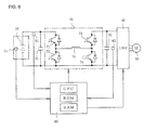
Fig. 6 is a circuit diagram showing the heretofore known technology described in PTL 3. - In
Fig. 6 , 70 is a DC/DC converter which operates as a buck-boost chopper, 71 to 74 are semiconductor switches, and 75 is a reactor, wherein the series circuit of thesemiconductor switches current power source 10 andcapacitor 31, and the series circuit of thesemiconductor switches capacitor 32 andinverter 40. 11 and 62 are voltage detectors, 61 is a current detector, and 80 is a control circuit. - In the heretofore known technology, the duty ratio of the
semiconductor switches DC converter 70 is controlled, thereby changing energy stored in thereactor 75, and the voltage of the directcurrent power source 10 is controlled to a desired size and output to thecapacitor 32 side. - A circuit substantially the same as in
Fig. 6 is also described in NPL 1. -
- PTL 1:
JP-A-2004-120844 Fig. 2 ,5 ,6 , or the like) - PTL 2:
JP-A-2011-41336 Fig. 1 or the like) - PTL 3:
JP-A-2004-350478 Fig. 1 , 7, or the like) - NPL 1: Comparative Evaluation of Soft-Switching Concepts for Bi-directional Buck+Boost Dc-Dc Converters, p. 1856-1865, The 2010 International Power Electronics Conference (
Fig. 1 ) - The heretofore known technologies shown in
Figs. 4 and6 have a problem that thereactors respective converters - Also, the heretofore known technology of
Fig. 5 has a problem that as theinverter 40 is caused to operate as a zero-phase converter by appropriately switching theinverter 40 in the operation of switching theinverter 40 which drives the alternatingcurrent motor 50, a boost operation is constantly carried out while the alternatingcurrent motor 50 is operating, due to which the loss in theinverter 40 and alternatingcurrent motor 50 increases. - Furthermore, in the heretofore known technology of
Fig. 5 , by adjusting the on-duty of all the semiconductor switches in the upper arm or lower arm of theinverter 40, it is possible to control the direct current voltage of the inverter 40 (the voltage of the capacitor 30) in accordance with the rotation speed of the alternatingcurrent motor 50, and it is possible, for example, when the alternatingcurrent motor 50 rotates at high speed, to control the direct current voltage of theinverter 40 to a higher value than the voltage of the directcurrent power source 10, but the degree of freedom of the direct current voltage, and thus the alternating current output voltage, of theinverter 40 is generally low. - Therefore, a problem to be solved by the invention is to provide a power conversion system wherein by eliminating the need for a boost reactor and constant boost operation, it is possible to achieve a reduction in the size of the whole system and a loss reduction, and to enhance the degree of freedom of the direct current voltage of an inverter, and a control method of the power conversion system.
- In order to solve the heretofore described problem, a power conversion system according to
claim 1 includes a power storage device such as a capacitor; an inverter, between the positive and negative direct current terminals of which the power storage device is connected, and between a plurality of alternating current terminals of which a load having an inductance is connected; a first upper and lower arm portion, configured by connecting first and second semiconductor switches in series, of which the connection point of the first and second semiconductor switches is connected to the neutral point of the load; and a direct current power source such as a battery connected in parallel to the first upper and lower arm portion, wherein at least one pair of homopolar terminals, of pairs of homopolar terminals out of the positive and negative direct current terminals of the inverter and the positive and negative terminals of the first upper and lower arm portion, are connected by a switch, and the other pair of homopolar terminals are set at the same potential. - Herein, as according to claim 2, it is also good that only one pair of homopolar terminals, of pairs of homopolar terminals out of the positive and negative direct current terminals of the inverter and the positive and negative terminals of the first upper and lower arm portion, are connected by a switch, and the other pair of homopolar terminals are directly connected together.
- Alternatively, as according to claim 3, it is also good that pairs of homopolar terminals, of the positive and negative direct current terminals of the inverter and the positive and negative terminals of the first upper and lower arm portion, are connected one pair by each switch, and that one switch is constantly placed in an on state, and the other switch is brought into an on and off operation.
- As according to
claim 4, semiconductor switches configuring the inverter and the first and second semiconductor switches configuring the first upper and lower arm portion are each configured of a semiconductor switching element and a reflux diode connected in reverse parallel thereto. - Also, as according to
claim 5, it is desirable that as the load, an alternating current motor is connected, and that a leakage inductance of the alternating current motor is utilized as a boost inductance. - As a control method of the power conversion system according to the invention, as according to claim 6, it is possible that by switching the plurality of semiconductor switches configuring the inverter in a condition in which the switch is turned on and the first and second semiconductor switches are turned off, an alternating current voltage is output from the inverter to drive the load.
- Also, as according to
claim 7, it is also possible that the switch in claim 2 is turned off, and all the semiconductor switches in the upper arm or lower arm of the inverter are turned on or off at the same time, thereby equivalently configuring a second upper and lower arm portion formed of the series circuit of third and fourth semiconductor switches, and that the first and second semiconductor switches are turned on and off, thereby causing a buck-boost chopper formed of the first upper and lower arm portion, the second upper and lower arm portion, and the inductance of the load to operate, thus charging and discharging the capacitor. - Alternatively, as according to claim 8, it is also possible that in a condition in which one switch in claim 3 is constantly turned on, the other switch is turned off, and all the semiconductor switches in the upper arm or lower arm of the inverter are turned on or off at the same time, thereby equivalently configuring a second upper and lower arm portion formed of the series circuit of third and fourth semiconductor switches, and that the first and second semiconductor switches are turned on and off, thereby causing a buck-boost chopper formed of the first upper and lower arm portion, the second upper and lower arm portion, and the inductance of the load to operate, thus charging and discharging the capacitor.
- Furthermore, as according to
claim 9 or 10, by adopting an arrangement such that a switching pattern of the inverter for carrying out a buck-boost operation by the second upper and lower arm portion configures one portion of a switching pattern for outputting an alternating current voltage from the inverter to drive the load, it is possible to drive the load with the inverter while carrying out a buck-boost operation for the capacitor. - According to the invention, as the need for a boost reactor is eliminated by utilizing an inductance which a load such as an alternating current motor has, it is possible to reduce the size and price of the whole system. Also, as it is possible to select an operation mode in which the load is driven by an inverter without using a boost operation, a simplification in control is achieved, and a loss reduction is possible, compared with a heretofore known technology wherein a boost operation is constantly carried out.
- Furthermore, by enhancing the degree of freedom of the direct current voltage of the inverter, it is possible, when the load is, for example, an alternating current motor, to raise the direct current voltage of the inverter when the motor rotates at high speed, meaning that it is possible to reduce current with the motor set to be of high voltage specifications, and thus achieve a reduction in the diameter of a cable through which to supply power to the motor, a reduction in the size of connection terminals, and the like.
-
- [
Fig. 1] Fig. 1 is a circuit diagram showing an embodiment of the invention. - [
Fig. 2] Fig. 2 is an equivalent circuit diagram ofFig. 1 . - [
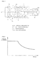
Fig. 3] Fig. 3 is a schematic characteristic diagram showing a relationship between the speed and torque (current) of an alternating current motor. - [
Fig. 4] Fig. 4 is a circuit diagram showing a heretofore known technology. - [
Fig. 5] Fig. 5 is a circuit diagram showing a heretofore known technology. - [
Fig. 6] Fig. 6 is a circuit diagram showing a heretofore known technology. - Hereafter, a description will be given, along the drawings, of an embodiment of the invention.
-
Fig. 1 is a circuit diagram showing an embodiment of the invention. InFig. 1 , the positive and negative direct current terminals of a three-phase voltage inverter 40 formed ofsemiconductor switches 41 to 46 are connected one to each end of acapacitor 30 acting as a power storage device, and a three-phase alternatingcurrent motor 50 is connected to the alternating current terminals of theinverter 40. - Meanwhile, an upper and
lower arm portion 90 whereinsemiconductor switches current power source 10 formed of a battery or the like, and the connection point of thesemiconductor switches neutral point 50a of the alternatingcurrent motor 50. Herein, thesemiconductor switches lower arm portion 90 is called a first upper and lower arm portion. - Also, the positive terminal of the upper and lower arm portion 90 (the positive pole of the direct current power source 10) is connected to one direct current terminal (positive terminal) of the
inverter 40 via aswitch 100 formed of a bidirectional semiconductor switch or a mechanical switch, while the negative terminal of the upper and lower arm portion 90 (the negative pole of the direct current power source 10) is directly connected to the other direct current terminal (negative terminal) of theinverter 40, and both negative terminals are kept at the same potential. - A configuration may be such that the
switch 100 is connected between the negative terminal of the upper andlower arm portion 90 and the negative terminal of theinverter 40, and that the positive terminal of the upper andlower arm portion 90 and the positive terminal of theinverter 40 are directly connected together and kept at the same potential. - Also, although not shown, switches may be connected, one between the positive terminal of the upper and
lower arm portion 90 and the positive terminal of the inverter, and the other between the negative terminal of the upper andlower arm portion 90 and the negative terminal of the inverter. In this case, a configuration only has to be such that while a power conversion system is operating, one switch (which corresponds to theswitch 100 of the embodiment) is turned on or off by an operation, to be described hereafter, while the other switch is constantly placed in an on state, and both ends of the other switch are kept at the same potential, and that when the power conversion system stops, the other switch is turned off. - In the heretofore described configuration, the
semiconductor switches 41 to 46, 91, and 92 are each configured of a semiconductor switching element, such as an IGBT, and a reflux diode connected in reverse parallel thereto, as illustrated in the brackets inFig. 1 . - Next, a description will be given of an operation of the embodiment.
- When the
switch 100 inFig. 1 is turned on, and thesemiconductor switches lower arm portion 90 are turned off, the directcurrent power source 10 and thecapacitor 30 are connected in parallel to the direct current circuit of theinverter 40, thus configuring an alternating current motor drive system, formed of a common three-phase voltage inverter, as the whole circuit. Because of this, theinverter 40, by carrying out PWM control or the like in accordance with a predetermined voltage command given from a control circuit (not shown) and thus turning on and off thesemiconductor switches 41 to 46, converts a direct current voltage to a three-phase alternating current voltage and supplies the three-phase alternating voltage to the alternatingcurrent motor 50. - Next, when a switching operation wherein all the semiconductor switches in the upper arm or lower arm of the
inverter 40 are turned on or off to control a zero-phase voltage (theinverter 40 is caused to operate as a zero-phase converter) , and a switching operation of theinverter 40 by a positive phase voltage command, are carried out in a time-division manner in a condition in which theswitch 100 is turned off, the circuit inFig. 1 changes equivalently to the kind of circuit inFig. 2 . - In
Fig. 2 , 40A is an upper and lower arm portion which equivalently shows theinverter 40 acting as a zero-phase converter, and an upper-arm semiconductor switch 47 corresponds to the semiconductor switches 41, 43, and 45 inFig. 1 which are turned on or off at the same time, while a lower-arm semiconductor switch 48 corresponds to the semiconductor switches 42, 44, and 46 inFig. 1 which are turned off or on at the same time. Herein, the semiconductor switches 47 and 48 configuring the upper andlower arm portion 40A are called third and fourth semiconductor switches, and the upper andlower arm portion 40A is called a second upper and lower arm portion. - With the circuit configuration shown in
Fig. 1 , the connection point of the semiconductor switches 47 and 48 inFig. 2 is connected to the connection point of the semiconductor switches 91 and 92 of the upper andlower arm portion 90 via a leakage inductance (a zero-phase inductance) 51 of the alternatingcurrent motor 50, and a buck-boost converter 70A is configured of the upper andlower arm portions leakage inductance 51. - The circuit shown in
Fig. 2 is substantially the same in overall configuration as the previously described circuit inFig. 6 , and the buck-boost converter 70A inFig. 2 has the same function as circuits described in, for example,Fig. 3 inJapanese Patent No. 3, 666, 557 Figs. 1 and2 inJapanese Patent No. 5,029,315 - As is obvious from these pieces of known literature, when the positive phase voltage command and the zero-phase voltage command are synthesized and given to the semiconductor switches 41 to 46 configuring the
inverter 40 inFig. 1 , it is possible, firstly, to convert the voltage of thecapacitor 30 to a three-phase alternating current voltage by a normal inverter operation in accordance with the positive phase voltage command, and apply the three-phase alternating current voltage to the alternatingcurrent motor 50. - Also, the zero-phase voltage of the
inverter 40 is controlled in accordance with the zero-phase voltage command, and zero-phase power is exchanged between the directcurrent power source 10 and thecapacitor 30 by the switching operations of the upper andlower arm portion 40A acting as an equivalently configured zero-phase converter and of the other upper andlower arm portion 90, thus enabling a buck-boost operation to be carried out. For example, when the semiconductor switches 42, 44, and 46 in the lower arm of theinverter 40 inFig. 1 are turned on at the same time (thesemiconductor switch 48 inFig. 2 is turned on), and thesemiconductor switch 91 of the upper andlower arm portion 90 is turned on, by the zero-phase voltage command, energy is stored in theleakage inductance 51 from the directcurrent power source 10. Next, when the semiconductor switches 42, 44, and 46 in the lower arm of theinverter 40 inFig. 1 are turned off at the same time (thesemiconductor switch 48 inFig. 2 is turned off) and thesemiconductor switch 91 is turned off, the energy stored in theleakage inductance 51 is supplied to thecapacitor 30 via the reflux diodes of the semiconductor switches 41, 43, and 45 (thesemiconductor switch 47 inFig. 2 ) and the reflux diode of thesemiconductor switch 92, meaning that it is possible to charge thecapacitor 30. When turning off the semiconductor switches 42, 44, and 46 at the same time, thesemiconductor switch 91 may be maintained in an on state. - That is, the buck-
boost capacitor 70A inFig. 2 is such that the semiconductor switches 47 and 48 of the upper andlower arm portion 40A and the semiconductor switches 91 and 92 of the upper andlower arm portion 90 inFigs. 1 and2 are turned on and off, thereby causing current to flow from the directcurrent power source 10 to theleakage inductance 51 inFig. 2 and thus storing energy in theleakage inductance 51, and furthermore, the energy is supplied to thecapacitor 30 via the reflux diodes of the semiconductor switches 47 and 92 inFig. 2 , meaning that it is possible to charge thecapacitor 30 using the energy of the directcurrent power source 10. - Herein, the semiconductor switches 91 and 92 of the upper and
lower arm portion 90 and theleakage inductance 51 operate as a buck chopper, and the semiconductor switches 47 and 48 of the upper andlower arm portion 40A and theleakage inductance 51 operate as a boost chopper. Therefore, by adjusting the duty ratio of the semiconductor switches 91, 92, 47, and 48 configuring the buck and boost choppers, it is possible to control the direct current voltage of the inverter 40 (the voltage of the capacitor 30), and thus the alternating current output voltage of theinverter 40, with respect to the voltage of the directcurrent power source 10 at a high degree of freedom. - In the embodiment, as heretofore described, in a condition in which the
switch 100 inFig. 1 is turned on and the semiconductor switches 91 and 92 of the upper andlower arm portion 90 are turned off, it is possible to drive the alternatingcurrent motor 50 by the normal operation of theinverter 40 to which the directcurrent power source 10 is directly connected. As no boost operation is carried out in this operation mode, control is simplified, and no loss occurs either due to the neutral point current of the alternatingcurrent motor 50, compared with a heretofore known technology wherein the boost operation is constantly carried out while theinverter 40 is operating, as inFig. 5 . - Also, when turning off the
switch 100 inFig. 1 and thus causing theinverter 40 to operate as a zero-phase converter, and switching the semiconductor switches 91 and 92 of the upper andlower arm portion 90, it is possible to carry out a buck-boost operation utilizing theleakage inductance 51 even without using a reactor, as heretofore known, meaning that it is possible to reduce the size and price of the whole system. - At the same time, as the buck-
boost converter 70A is caused to operate as a buck-boost chopper, as previously described, the degree of freedom of the direct current voltage of theinverter 40 is high, and it is thus possible to output a desired size of alternating current voltage to drive the alternatingcurrent motor 50. - Furthermore, as a permanent magnet synchronous motor used in, for example, an electric vehicle or a hybrid car, in general, having the kinds of speed-torque characteristics shown in
Fig. 3 , is such that the current of the motor is substantially proportional to the torque, it may be conceivable that the speed-current characteristics of the motor are also substantially the same as inFig. 4 . - According to
Fig. 3 , as less current is needed in a higher speed region of the motor, in other words, there is much room for being able to cause the neutral point current (zero-phase current) to flow with respect to a preset heat generation amount, the embodiment is suitable for a kind of case in which a boost operation is carried out in a high speed region which does not require so much torque. - As the terminal voltage of the alternating current motor, in general, rises along with an increase in rotation speed, in the event that it is possible to carry out a boost operation, it is possible, in accordance therewith, to design the terminal voltage of the motor to be a high voltage. As a result of this, current flowing through the motor is suppressed, thus enabling a contribution to a reduction in the diameter of a cable through which to supply power to the motor, a reduction in the size of connection terminals and semiconductor elements, and a reduction in the size, weight, and cost of the whole system owing to the reduced volume.
- The invention can be utilized in each kind of drive system wherein a load is driven by an inverter, including an in-vehicle power conversion system mounted on, for example, an electric vehicle or hybrid car.
-
- 10: Direct current power source
- 30: Capacitor
- 40: Inverter
- 40A: Second upper and lower arm portion
- 41 to 48: Semiconductor switches
- 50: Alternating current motor
- 50a: Neutral point
- 70A: Buck-boost converter
- 90: First upper and lower arm portion
- 91, 92: Semiconductor switch
- 100: Switch
Claims (10)
- A power conversion system, comprising:a power storage device which stores direct current power;an inverter, between the positive and negative direct current terminals of which the power storage device is connected, and between a plurality of alternating current terminals of which a load having an inductance is connected;a first upper and lower arm portion, configured by connecting first and second semiconductor switches in series, of which the connection point of the first and second semiconductor switches is connected to the neutral point of the load; anda direct current power source connected in parallel to the first upper and lower arm portion, the power conversion system being characterized in thatat least one pair of homopolar terminals, of pairs of homopolar terminals out of the positive and negative direct current terminals of the inverter and the positive and negative terminals of the first upper and lower arm portion, are connected by a switch, and the other pair of homopolar terminals are set at the same potential.
- The power conversion system according to claim 1, characterized in that
only one pair of homopolar terminals, of pairs of homopolar terminals out of the positive and negative direct current terminals of the inverter and the positive and negative terminals of the first upper and lower arm portion, are connected by a switch, and the other pair of homopolar terminals are directly connected together. - The power conversion system according to claim 1, characterized in that
pairs of homopolar terminals, of the positive and negative direct current terminals of the inverter and the positive and negative terminals of the first upper and lower arm portion, are connected one pair by each switch. - The power conversion system according to claim 1, characterized in that
semiconductor switches configuring the inverter and the first and second semiconductor switches configuring the first upper and lower arm portion are each configured of a semiconductor switching element and a reflux diode connected in reverse parallel thereto. - The power conversion system according to claim 1, characterized in that
the load is an alternating current motor, and the inductance which the load has is a leakage inductance of the alternating current motor. - A method for controlling the power conversion system according to any one of claims 1 to 5, characterized in that
by switching the plurality of semiconductor switches configuring the inverter in a condition in which the switch is turned on and the first and second semiconductor switches are turned off, an alternating current voltage is output from the inverter to drive the load. - The method for controlling the power conversion system according to claim 2, characterized in that
the switch is turned off, and all the semiconductor switches in the upper arm or lower arm of the inverter are turned on or off at the same time, thereby equivalently configuring a second upper and lower arm portion formed of the series circuit of third and fourth semiconductor switches, and that the first and second semiconductor switches are turned on and off, thereby causing a buck-boost chopper formed of the first upper and lower arm portion, the second upper and lower arm portion, and the inductance of the load to operate, thus charging and discharging the capacitor. - The method for controlling the power conversion system according to claim 3, characterized in that
in a condition in which one switch is constantly turned on, the other switch is turned off, and all the semiconductor switches in the upper arm or lower arm of the inverter are turned on or off at the same time, thereby equivalently configuring a second upper and lower arm portion formed of the series circuit of third and fourth semiconductor switches, and that the first and second semiconductor switches are turned on and off, thereby causing a buck-boost chopper formed of the first upper and lower arm portion, the second upper and lower arm portion, and the inductance of the load to operate, thus charging and discharging the capacitor. - The method of claim 6 for controlling the power conversion system, characterized in that
a switching pattern of the inverter for carrying out a buck-boost operation by the second upper and lower arm portion configures one portion of a switching pattern for outputting an alternating current voltage from the inverter to drive the load. - The method of claim 7 or 8 for controlling the power conversion system, characterized in that
a switching pattern of the inverter for carrying out a buck-boost operation by the second upper and lower arm portion configures one portion of a switching pattern for outputting an alternating current voltage from the inverter to drive the load.
Applications Claiming Priority (2)
| Application Number | Priority Date | Filing Date | Title |
|---|---|---|---|
| JP2012259641 | 2012-11-28 | ||
| PCT/JP2013/078907 WO2014083980A1 (en) | 2012-11-28 | 2013-10-25 | Power conversion system and method for controlling same |
Publications (3)
| Publication Number | Publication Date |
|---|---|
| EP2928061A1 true EP2928061A1 (en) | 2015-10-07 |
| EP2928061A4 EP2928061A4 (en) | 2017-03-08 |
| EP2928061B1 EP2928061B1 (en) | 2018-01-10 |
Family
ID=50827626
Family Applications (1)
| Application Number | Title | Priority Date | Filing Date |
|---|---|---|---|
| EP13858200.2A Not-in-force EP2928061B1 (en) | 2012-11-28 | 2013-10-25 | Power conversion system and method for controlling same |
Country Status (5)
| Country | Link |
|---|---|
| US (1) | US9843278B2 (en) |
| EP (1) | EP2928061B1 (en) |
| JP (1) | JP5858309B2 (en) |
| CN (1) | CN104737435B (en) |
| WO (1) | WO2014083980A1 (en) |
Families Citing this family (14)
| Publication number | Priority date | Publication date | Assignee | Title |
|---|---|---|---|---|
| KR101606679B1 (en) * | 2013-04-09 | 2016-03-25 | 미쓰비시덴키 가부시키가이샤 | Multiaxial driving apparatus |
| FR3056037B1 (en) * | 2016-09-14 | 2018-08-17 | Valeo Equipements Electriques Moteur | ELECTRIC POWER TRANSFER SYSTEM |
| US10250059B2 (en) * | 2016-09-19 | 2019-04-02 | Microsoft Technology Licensing, Llc | Charging circuit for battery-powered device |
| KR101966501B1 (en) * | 2016-10-26 | 2019-08-14 | 현대자동차주식회사 | Charging system for wound rotor synchronous motor |
| KR101936992B1 (en) * | 2016-10-26 | 2019-01-10 | 현대자동차주식회사 | Charging system for wound rotor synchronous motor |
| CN108347167B (en) * | 2017-01-25 | 2021-07-13 | 通用电气公司 | System and method for soft-switching DC-DC converters |
| DE102018120236A1 (en) * | 2018-08-20 | 2020-02-20 | Thyssenkrupp Ag | Charging device with controllable intermediate circuit center voltage and drive system with such a charging device |
| JP7160479B2 (en) * | 2018-12-21 | 2022-10-25 | 株式会社デンソー | electric motor system |
| JP7294982B2 (en) * | 2019-10-18 | 2023-06-20 | 株式会社豊田中央研究所 | motor controller |
| CN113119801B (en) * | 2019-12-31 | 2023-12-12 | 比亚迪股份有限公司 | Vehicle, energy conversion device and control method thereof |
| CN113752909B (en) * | 2020-06-04 | 2023-08-08 | 比亚迪股份有限公司 | Energy conversion device and vehicle |
| EP3988377B1 (en) * | 2020-10-23 | 2024-01-03 | Ningbo Geely Automobile Research & Development Co. Ltd. | A vehicle electrical system |
| JP7446390B2 (en) * | 2021-11-08 | 2024-03-08 | 台達電子工業股▲ふん▼有限公司 | Integrated power system with motor drive and battery charging/discharging |
| CN118232760A (en) * | 2022-12-14 | 2024-06-21 | 采埃孚股份公司 | Electric drive system, control method and related equipment |
Family Cites Families (45)
| Publication number | Priority date | Publication date | Assignee | Title |
|---|---|---|---|---|
| FR2692734B1 (en) * | 1992-06-23 | 1994-08-26 | Auxilec | Electric traction chain for motor vehicle. |
| US5502368A (en) * | 1994-06-06 | 1996-03-26 | Ecoair Corp. | Hybrid alternator with voltage regulator |
| US5397975A (en) * | 1993-06-14 | 1995-03-14 | Ecoair Corp. | Hybrid alternator |
| US5491622A (en) * | 1994-01-07 | 1996-02-13 | Delco Electronics Corp. | Power converter with emergency operating mode for three phase induction motors |
| JP3741171B2 (en) * | 1996-06-17 | 2006-02-01 | 株式会社安川電機 | Multiple pulse width modulation power converter |
| DE19823917A1 (en) * | 1997-06-03 | 1998-12-10 | Fuji Electric Co Ltd | Converter for producing multiphase AC current |
| JP3666557B2 (en) | 1999-04-20 | 2005-06-29 | 富士電機機器制御株式会社 | Power conversion circuit |
| US6291963B2 (en) * | 1999-12-15 | 2001-09-18 | Nissan Motor Co., Ltd. | Drive circuit for motor/generator |
| JP3775468B2 (en) * | 2000-01-19 | 2006-05-17 | 富士電機システムズ株式会社 | AC motor variable speed drive system |
| US6518736B2 (en) * | 2000-06-26 | 2003-02-11 | Toyota Jidosha Kabushiki Kaisha | Mechanical power outputting apparatus and inverter apparatus |
| JP3721116B2 (en) | 2000-11-14 | 2005-11-30 | 株式会社豊田中央研究所 | DRIVE DEVICE, POWER OUTPUT DEVICE, AND CONTROL METHOD THEREOF |
| JP4725694B2 (en) * | 2001-02-01 | 2011-07-13 | 富士電機システムズ株式会社 | PWM power converter control device |
| JP2003102181A (en) * | 2001-09-25 | 2003-04-04 | Toyota Motor Corp | Power supply system and power supply method |
| JP3692993B2 (en) * | 2001-10-04 | 2005-09-07 | トヨタ自動車株式会社 | DRIVE DEVICE AND POWER OUTPUT DEVICE |
| JP4023171B2 (en) * | 2002-02-05 | 2007-12-19 | トヨタ自動車株式会社 | LOAD DRIVE DEVICE, CHARGE CONTROL METHOD FOR POWER STORAGE DEVICE IN LOAD DRIVE DEVICE, AND COMPUTER-READABLE RECORDING MEDIUM CONTAINING PROGRAM FOR CAUSING COMPUTER TO EXECUTE CHARGE CONTROL |
| JP2004120844A (en) | 2002-09-25 | 2004-04-15 | Fuji Electric Systems Co Ltd | Boost converter controller |
| JP4111059B2 (en) | 2003-05-26 | 2008-07-02 | トヨタ自動車株式会社 | Voltage conversion system, voltage conversion method, and control program |
| JP4063199B2 (en) * | 2003-11-14 | 2008-03-19 | 日産自動車株式会社 | Control device for motor-driven 4WD vehicle |
| JP3993564B2 (en) * | 2004-01-13 | 2007-10-17 | 三菱重工業株式会社 | Series hybrid electric vehicle |
| GB0415153D0 (en) * | 2004-07-06 | 2004-08-11 | Newage Int Ltd | Electrical machine rotor position identification |
| JP4517994B2 (en) * | 2005-09-29 | 2010-08-04 | トヨタ自動車株式会社 | Charge control device and electric vehicle |
| FR2892243B1 (en) * | 2005-10-13 | 2008-01-18 | Airbus France Sas | RECONFIGURABLE VOLTAGE INVERTER WITH TROUBLESHOOTING |
| JP2007220976A (en) * | 2006-02-17 | 2007-08-30 | Toyota Motor Corp | Semiconductor module and drive device for hybrid vehicle including the same |
| JP4747968B2 (en) * | 2006-06-30 | 2011-08-17 | トヨタ自動車株式会社 | Motor drive device |
| US7609050B2 (en) * | 2007-02-20 | 2009-10-27 | Gm Global Technology Operations, Inc. | Method and system for determing current in an electrical component in a power conversion system |
| EP1990908B1 (en) * | 2007-05-10 | 2010-03-31 | Denso Corporation | Rotary electric system designed to utilize zero-phase circuit |
| JP4483911B2 (en) * | 2007-08-31 | 2010-06-16 | 株式会社デンソー | Rotating electric machine for vehicles |
| BRPI0816660A2 (en) * | 2007-09-10 | 2015-03-10 | Toyota Motor Co Ltd | APPARATUS AND METHOD FOR ACTIVATE VEHICLE SYSTEM |
| JP4609474B2 (en) * | 2007-10-10 | 2011-01-12 | 株式会社デンソー | Rotating electrical machine equipment |
| JP5040585B2 (en) * | 2007-10-24 | 2012-10-03 | 富士電機株式会社 | Power conversion system |
| JP5029315B2 (en) | 2007-11-22 | 2012-09-19 | 富士電機株式会社 | Motor drive system |
| JP4441920B2 (en) * | 2007-11-22 | 2010-03-31 | 株式会社デンソー | Power supply |
| JP5527497B2 (en) * | 2008-01-11 | 2014-06-18 | 富士電機株式会社 | AC motor drive circuit and electric vehicle drive circuit |
| JP4719776B2 (en) * | 2008-07-14 | 2011-07-06 | トヨタ自動車株式会社 | Charging cable, charging control device, and vehicle charging system |
| JP5251413B2 (en) * | 2008-10-14 | 2013-07-31 | 株式会社デンソー | Synchronous motor drive device |
| JP5412974B2 (en) * | 2009-03-13 | 2014-02-12 | 株式会社デンソー | Driving device for three-phase AC synchronous motor |
| JP4800402B2 (en) * | 2009-03-18 | 2011-10-26 | 株式会社豊田中央研究所 | Multi-phase converter for on-vehicle use |
| US8063440B2 (en) * | 2009-05-28 | 2011-11-22 | GM Global Technology Operations LLC | Power electronics power module with imbedded gate circuitry |
| JP5493568B2 (en) * | 2009-08-06 | 2014-05-14 | 株式会社デンソー | Electric motor drive device, electric motor drive device control method, and electric device |
| JP5434381B2 (en) * | 2009-08-31 | 2014-03-05 | 株式会社デンソー | In-vehicle motor drive system |
| EP2538543B1 (en) * | 2010-02-17 | 2019-08-21 | Fuji Electric Co., Ltd. | Power conversion apparatus |
| JP5104898B2 (en) * | 2010-04-28 | 2012-12-19 | トヨタ自動車株式会社 | Electric system power limiting device |
| FR2961361B1 (en) * | 2010-06-14 | 2013-07-12 | Hispano Suiza Sa | VOLTAGE INVERTER AND METHOD FOR CONTROLLING SUCH AS INVERTER |
| JP5365586B2 (en) * | 2010-06-18 | 2013-12-11 | 富士電機株式会社 | Power converter |
| JP2012235659A (en) * | 2011-05-09 | 2012-11-29 | Denso Corp | Controller of rotary machine |
-
2013
- 2013-10-25 EP EP13858200.2A patent/EP2928061B1/en not_active Not-in-force
- 2013-10-25 CN CN201380055337.6A patent/CN104737435B/en not_active Expired - Fee Related
- 2013-10-25 JP JP2014550090A patent/JP5858309B2/en not_active Expired - Fee Related
- 2013-10-25 WO PCT/JP2013/078907 patent/WO2014083980A1/en not_active Ceased
-
2015
- 2015-04-22 US US14/693,281 patent/US9843278B2/en not_active Expired - Fee Related
Non-Patent Citations (1)
| Title |
|---|
| See references of WO2014083980A1 * |
Also Published As
| Publication number | Publication date |
|---|---|
| EP2928061A4 (en) | 2017-03-08 |
| WO2014083980A1 (en) | 2014-06-05 |
| US20150229252A1 (en) | 2015-08-13 |
| CN104737435A (en) | 2015-06-24 |
| US9843278B2 (en) | 2017-12-12 |
| EP2928061B1 (en) | 2018-01-10 |
| JP5858309B2 (en) | 2016-02-10 |
| JPWO2014083980A1 (en) | 2017-01-05 |
| CN104737435B (en) | 2018-05-29 |
Similar Documents
| Publication | Publication Date | Title |
|---|---|---|
| US9843278B2 (en) | Power conversion system and control method thereof | |
| US11431184B2 (en) | Power supply device | |
| US8508961B2 (en) | Power conversion apparatus | |
| US20130002186A1 (en) | Power converter | |
| US20230226936A1 (en) | Vehicle electrical system | |
| KR101965558B1 (en) | System for coupling at least one dc source to a controllable energy store and associated operating method | |
| US12580391B2 (en) | System for charging vehicle battery using motor driving system | |
| JP6439282B2 (en) | Charging system, power supply vehicle, charging vehicle, and charging method | |
| KR20230013551A (en) | System of charging battery for vehicle using motor driving system | |
| JP5288178B2 (en) | Motor drive system | |
| US20130249474A1 (en) | System for Charging an Energy Store, and Method for Operating the Charging System | |
| US9793850B2 (en) | Systems for charging an energy store, and method for operating the charging systems | |
| US9457683B2 (en) | Method for discharging at least one capacitor of an electric circuit | |
| EP4108507A1 (en) | System for charging vehicle battery using motor driving system | |
| US9112359B2 (en) | System for charging an energy store, and method for operating the charging system | |
| US20140361619A1 (en) | Power device | |
| KR101036163B1 (en) | 3-phase electric motor drive | |
| JP5122200B2 (en) | Drive controller for buck-boost converter and buck-boost converter | |
| JP5629667B2 (en) | Multi-phase converter | |
| CN105075103B (en) | multi-axis drive | |
| US9178365B2 (en) | System for charging an energy store, and method for operating the charging system | |
| JP5348484B2 (en) | Load drive system | |
| EP4579996A1 (en) | Charging system |
Legal Events
| Date | Code | Title | Description |
|---|---|---|---|
| PUAI | Public reference made under article 153(3) epc to a published international application that has entered the european phase |
Free format text: ORIGINAL CODE: 0009012 |
|
| 17P | Request for examination filed |
Effective date: 20150427 |
|
| AK | Designated contracting states |
Kind code of ref document: A1 Designated state(s): AL AT BE BG CH CY CZ DE DK EE ES FI FR GB GR HR HU IE IS IT LI LT LU LV MC MK MT NL NO PL PT RO RS SE SI SK SM TR |
|
| AX | Request for extension of the european patent |
Extension state: BA ME |
|
| DAX | Request for extension of the european patent (deleted) | ||
| RA4 | Supplementary search report drawn up and despatched (corrected) |
Effective date: 20170207 |
|
| RIC1 | Information provided on ipc code assigned before grant |
Ipc: H02M 1/00 20070101ALN20170201BHEP Ipc: H02M 7/5387 20070101AFI20170201BHEP Ipc: H02M 3/158 20060101ALI20170201BHEP |
|
| GRAP | Despatch of communication of intention to grant a patent |
Free format text: ORIGINAL CODE: EPIDOSNIGR1 |
|
| RIC1 | Information provided on ipc code assigned before grant |
Ipc: H02M 7/5387 20070101AFI20170705BHEP Ipc: H02M 1/00 20070101ALN20170705BHEP Ipc: H02M 3/158 20060101ALI20170705BHEP |
|
| RIC1 | Information provided on ipc code assigned before grant |
Ipc: H02M 7/5387 20070101AFI20170714BHEP Ipc: H02M 3/158 20060101ALI20170714BHEP Ipc: H02M 1/00 20070101ALN20170714BHEP |
|
| INTG | Intention to grant announced |
Effective date: 20170810 |
|
| GRAS | Grant fee paid |
Free format text: ORIGINAL CODE: EPIDOSNIGR3 |
|
| GRAA | (expected) grant |
Free format text: ORIGINAL CODE: 0009210 |
|
| AK | Designated contracting states |
Kind code of ref document: B1 Designated state(s): AL AT BE BG CH CY CZ DE DK EE ES FI FR GB GR HR HU IE IS IT LI LT LU LV MC MK MT NL NO PL PT RO RS SE SI SK SM TR |
|
| REG | Reference to a national code |
Ref country code: CH Ref legal event code: EP Ref country code: AT Ref legal event code: REF Ref document number: 963477 Country of ref document: AT Kind code of ref document: T Effective date: 20180115 |
|
| REG | Reference to a national code |
Ref country code: IE Ref legal event code: FG4D |
|
| REG | Reference to a national code |
Ref country code: DE Ref legal event code: R096 Ref document number: 602013032208 Country of ref document: DE |
|
| REG | Reference to a national code |
Ref country code: NL Ref legal event code: MP Effective date: 20180110 |
|
| REG | Reference to a national code |
Ref country code: AT Ref legal event code: MK05 Ref document number: 963477 Country of ref document: AT Kind code of ref document: T Effective date: 20180110 |
|
| PG25 | Lapsed in a contracting state [announced via postgrant information from national office to epo] |
Ref country code: NL Free format text: LAPSE BECAUSE OF FAILURE TO SUBMIT A TRANSLATION OF THE DESCRIPTION OR TO PAY THE FEE WITHIN THE PRESCRIBED TIME-LIMIT Effective date: 20180110 |
|
| PG25 | Lapsed in a contracting state [announced via postgrant information from national office to epo] |
Ref country code: FI Free format text: LAPSE BECAUSE OF FAILURE TO SUBMIT A TRANSLATION OF THE DESCRIPTION OR TO PAY THE FEE WITHIN THE PRESCRIBED TIME-LIMIT Effective date: 20180110 Ref country code: NO Free format text: LAPSE BECAUSE OF FAILURE TO SUBMIT A TRANSLATION OF THE DESCRIPTION OR TO PAY THE FEE WITHIN THE PRESCRIBED TIME-LIMIT Effective date: 20180410 Ref country code: CY Free format text: LAPSE BECAUSE OF FAILURE TO SUBMIT A TRANSLATION OF THE DESCRIPTION OR TO PAY THE FEE WITHIN THE PRESCRIBED TIME-LIMIT Effective date: 20180110 Ref country code: ES Free format text: LAPSE BECAUSE OF FAILURE TO SUBMIT A TRANSLATION OF THE DESCRIPTION OR TO PAY THE FEE WITHIN THE PRESCRIBED TIME-LIMIT Effective date: 20180110 Ref country code: HR Free format text: LAPSE BECAUSE OF FAILURE TO SUBMIT A TRANSLATION OF THE DESCRIPTION OR TO PAY THE FEE WITHIN THE PRESCRIBED TIME-LIMIT Effective date: 20180110 Ref country code: LT Free format text: LAPSE BECAUSE OF FAILURE TO SUBMIT A TRANSLATION OF THE DESCRIPTION OR TO PAY THE FEE WITHIN THE PRESCRIBED TIME-LIMIT Effective date: 20180110 |
|
| PG25 | Lapsed in a contracting state [announced via postgrant information from national office to epo] |
Ref country code: GR Free format text: LAPSE BECAUSE OF FAILURE TO SUBMIT A TRANSLATION OF THE DESCRIPTION OR TO PAY THE FEE WITHIN THE PRESCRIBED TIME-LIMIT Effective date: 20180411 Ref country code: AT Free format text: LAPSE BECAUSE OF FAILURE TO SUBMIT A TRANSLATION OF THE DESCRIPTION OR TO PAY THE FEE WITHIN THE PRESCRIBED TIME-LIMIT Effective date: 20180110 Ref country code: RS Free format text: LAPSE BECAUSE OF FAILURE TO SUBMIT A TRANSLATION OF THE DESCRIPTION OR TO PAY THE FEE WITHIN THE PRESCRIBED TIME-LIMIT Effective date: 20180110 Ref country code: BG Free format text: LAPSE BECAUSE OF FAILURE TO SUBMIT A TRANSLATION OF THE DESCRIPTION OR TO PAY THE FEE WITHIN THE PRESCRIBED TIME-LIMIT Effective date: 20180410 Ref country code: IS Free format text: LAPSE BECAUSE OF FAILURE TO SUBMIT A TRANSLATION OF THE DESCRIPTION OR TO PAY THE FEE WITHIN THE PRESCRIBED TIME-LIMIT Effective date: 20180510 Ref country code: SE Free format text: LAPSE BECAUSE OF FAILURE TO SUBMIT A TRANSLATION OF THE DESCRIPTION OR TO PAY THE FEE WITHIN THE PRESCRIBED TIME-LIMIT Effective date: 20180110 Ref country code: LV Free format text: LAPSE BECAUSE OF FAILURE TO SUBMIT A TRANSLATION OF THE DESCRIPTION OR TO PAY THE FEE WITHIN THE PRESCRIBED TIME-LIMIT Effective date: 20180110 Ref country code: PL Free format text: LAPSE BECAUSE OF FAILURE TO SUBMIT A TRANSLATION OF THE DESCRIPTION OR TO PAY THE FEE WITHIN THE PRESCRIBED TIME-LIMIT Effective date: 20180110 |
|
| REG | Reference to a national code |
Ref country code: DE Ref legal event code: R097 Ref document number: 602013032208 Country of ref document: DE |
|
| PG25 | Lapsed in a contracting state [announced via postgrant information from national office to epo] |
Ref country code: EE Free format text: LAPSE BECAUSE OF FAILURE TO SUBMIT A TRANSLATION OF THE DESCRIPTION OR TO PAY THE FEE WITHIN THE PRESCRIBED TIME-LIMIT Effective date: 20180110 Ref country code: RO Free format text: LAPSE BECAUSE OF FAILURE TO SUBMIT A TRANSLATION OF THE DESCRIPTION OR TO PAY THE FEE WITHIN THE PRESCRIBED TIME-LIMIT Effective date: 20180110 Ref country code: IT Free format text: LAPSE BECAUSE OF FAILURE TO SUBMIT A TRANSLATION OF THE DESCRIPTION OR TO PAY THE FEE WITHIN THE PRESCRIBED TIME-LIMIT Effective date: 20180110 Ref country code: AL Free format text: LAPSE BECAUSE OF FAILURE TO SUBMIT A TRANSLATION OF THE DESCRIPTION OR TO PAY THE FEE WITHIN THE PRESCRIBED TIME-LIMIT Effective date: 20180110 |
|
| PLBE | No opposition filed within time limit |
Free format text: ORIGINAL CODE: 0009261 |
|
| STAA | Information on the status of an ep patent application or granted ep patent |
Free format text: STATUS: NO OPPOSITION FILED WITHIN TIME LIMIT |
|
| PG25 | Lapsed in a contracting state [announced via postgrant information from national office to epo] |
Ref country code: SK Free format text: LAPSE BECAUSE OF FAILURE TO SUBMIT A TRANSLATION OF THE DESCRIPTION OR TO PAY THE FEE WITHIN THE PRESCRIBED TIME-LIMIT Effective date: 20180110 Ref country code: DK Free format text: LAPSE BECAUSE OF FAILURE TO SUBMIT A TRANSLATION OF THE DESCRIPTION OR TO PAY THE FEE WITHIN THE PRESCRIBED TIME-LIMIT Effective date: 20180110 Ref country code: SM Free format text: LAPSE BECAUSE OF FAILURE TO SUBMIT A TRANSLATION OF THE DESCRIPTION OR TO PAY THE FEE WITHIN THE PRESCRIBED TIME-LIMIT Effective date: 20180110 Ref country code: CZ Free format text: LAPSE BECAUSE OF FAILURE TO SUBMIT A TRANSLATION OF THE DESCRIPTION OR TO PAY THE FEE WITHIN THE PRESCRIBED TIME-LIMIT Effective date: 20180110 |
|
| 26N | No opposition filed |
Effective date: 20181011 |
|
| PG25 | Lapsed in a contracting state [announced via postgrant information from national office to epo] |
Ref country code: SI Free format text: LAPSE BECAUSE OF FAILURE TO SUBMIT A TRANSLATION OF THE DESCRIPTION OR TO PAY THE FEE WITHIN THE PRESCRIBED TIME-LIMIT Effective date: 20180110 |
|
| REG | Reference to a national code |
Ref country code: CH Ref legal event code: PL |
|
| GBPC | Gb: european patent ceased through non-payment of renewal fee |
Effective date: 20181025 |
|
| REG | Reference to a national code |
Ref country code: BE Ref legal event code: MM Effective date: 20181031 |
|
| PG25 | Lapsed in a contracting state [announced via postgrant information from national office to epo] |
Ref country code: LU Free format text: LAPSE BECAUSE OF NON-PAYMENT OF DUE FEES Effective date: 20181025 Ref country code: MC Free format text: LAPSE BECAUSE OF FAILURE TO SUBMIT A TRANSLATION OF THE DESCRIPTION OR TO PAY THE FEE WITHIN THE PRESCRIBED TIME-LIMIT Effective date: 20180110 |
|
| REG | Reference to a national code |
Ref country code: IE Ref legal event code: MM4A |
|
| PG25 | Lapsed in a contracting state [announced via postgrant information from national office to epo] |
Ref country code: BE Free format text: LAPSE BECAUSE OF NON-PAYMENT OF DUE FEES Effective date: 20181031 Ref country code: CH Free format text: LAPSE BECAUSE OF NON-PAYMENT OF DUE FEES Effective date: 20181031 Ref country code: LI Free format text: LAPSE BECAUSE OF NON-PAYMENT OF DUE FEES Effective date: 20181031 Ref country code: FR Free format text: LAPSE BECAUSE OF NON-PAYMENT OF DUE FEES Effective date: 20181031 |
|
| PG25 | Lapsed in a contracting state [announced via postgrant information from national office to epo] |
Ref country code: GB Free format text: LAPSE BECAUSE OF NON-PAYMENT OF DUE FEES Effective date: 20181025 Ref country code: IE Free format text: LAPSE BECAUSE OF NON-PAYMENT OF DUE FEES Effective date: 20181025 |
|
| PG25 | Lapsed in a contracting state [announced via postgrant information from national office to epo] |
Ref country code: MT Free format text: LAPSE BECAUSE OF NON-PAYMENT OF DUE FEES Effective date: 20181025 |
|
| PG25 | Lapsed in a contracting state [announced via postgrant information from national office to epo] |
Ref country code: TR Free format text: LAPSE BECAUSE OF FAILURE TO SUBMIT A TRANSLATION OF THE DESCRIPTION OR TO PAY THE FEE WITHIN THE PRESCRIBED TIME-LIMIT Effective date: 20180110 |
|
| PG25 | Lapsed in a contracting state [announced via postgrant information from national office to epo] |
Ref country code: PT Free format text: LAPSE BECAUSE OF FAILURE TO SUBMIT A TRANSLATION OF THE DESCRIPTION OR TO PAY THE FEE WITHIN THE PRESCRIBED TIME-LIMIT Effective date: 20180110 |
|
| PG25 | Lapsed in a contracting state [announced via postgrant information from national office to epo] |
Ref country code: HU Free format text: LAPSE BECAUSE OF FAILURE TO SUBMIT A TRANSLATION OF THE DESCRIPTION OR TO PAY THE FEE WITHIN THE PRESCRIBED TIME-LIMIT; INVALID AB INITIO Effective date: 20131025 Ref country code: MK Free format text: LAPSE BECAUSE OF NON-PAYMENT OF DUE FEES Effective date: 20180110 |
|
| PGFP | Annual fee paid to national office [announced via postgrant information from national office to epo] |
Ref country code: DE Payment date: 20230830 Year of fee payment: 11 |
|
| REG | Reference to a national code |
Ref country code: DE Ref legal event code: R119 Ref document number: 602013032208 Country of ref document: DE |
|
| PG25 | Lapsed in a contracting state [announced via postgrant information from national office to epo] |
Ref country code: DE Free format text: LAPSE BECAUSE OF NON-PAYMENT OF DUE FEES Effective date: 20250501 |