EP2927971A1 - Mounting substrate and light emitting apparatus using mounting substrate - Google Patents
Mounting substrate and light emitting apparatus using mounting substrate Download PDFInfo
- Publication number
- EP2927971A1 EP2927971A1 EP13858852.0A EP13858852A EP2927971A1 EP 2927971 A1 EP2927971 A1 EP 2927971A1 EP 13858852 A EP13858852 A EP 13858852A EP 2927971 A1 EP2927971 A1 EP 2927971A1
- Authority
- EP
- European Patent Office
- Prior art keywords
- mounting substrate
- layer
- light
- film
- substrate according
- Prior art date
- Legal status (The legal status is an assumption and is not a legal conclusion. Google has not performed a legal analysis and makes no representation as to the accuracy of the status listed.)
- Withdrawn
Links
Images
Classifications
-
- H—ELECTRICITY
- H10—SEMICONDUCTOR DEVICES; ELECTRIC SOLID-STATE DEVICES NOT OTHERWISE PROVIDED FOR
- H10H—INORGANIC LIGHT-EMITTING SEMICONDUCTOR DEVICES HAVING POTENTIAL BARRIERS
- H10H20/00—Individual inorganic light-emitting semiconductor devices having potential barriers, e.g. light-emitting diodes [LED]
- H10H20/80—Constructional details
- H10H20/85—Packages
- H10H20/857—Interconnections, e.g. lead-frames, bond wires or solder balls
-
- H—ELECTRICITY
- H05—ELECTRIC TECHNIQUES NOT OTHERWISE PROVIDED FOR
- H05K—PRINTED CIRCUITS; CASINGS OR CONSTRUCTIONAL DETAILS OF ELECTRIC APPARATUS; MANUFACTURE OF ASSEMBLAGES OF ELECTRICAL COMPONENTS
- H05K1/00—Printed circuits
- H05K1/02—Details
- H05K1/03—Use of materials for the substrate
- H05K1/05—Insulated conductive substrates, e.g. insulated metal substrate
- H05K1/053—Insulated conductive substrates, e.g. insulated metal substrate the metal substrate being covered by an inorganic insulating layer
-
- H—ELECTRICITY
- H10—SEMICONDUCTOR DEVICES; ELECTRIC SOLID-STATE DEVICES NOT OTHERWISE PROVIDED FOR
- H10H—INORGANIC LIGHT-EMITTING SEMICONDUCTOR DEVICES HAVING POTENTIAL BARRIERS
- H10H20/00—Individual inorganic light-emitting semiconductor devices having potential barriers, e.g. light-emitting diodes [LED]
- H10H20/80—Constructional details
- H10H20/85—Packages
- H10H20/852—Encapsulations
- H10H20/854—Encapsulations characterised by their material, e.g. epoxy or silicone resins
-
- H—ELECTRICITY
- H10—SEMICONDUCTOR DEVICES; ELECTRIC SOLID-STATE DEVICES NOT OTHERWISE PROVIDED FOR
- H10H—INORGANIC LIGHT-EMITTING SEMICONDUCTOR DEVICES HAVING POTENTIAL BARRIERS
- H10H20/00—Individual inorganic light-emitting semiconductor devices having potential barriers, e.g. light-emitting diodes [LED]
- H10H20/80—Constructional details
- H10H20/85—Packages
- H10H20/855—Optical field-shaping means, e.g. lenses
- H10H20/856—Reflecting means
-
- H—ELECTRICITY
- H10—SEMICONDUCTOR DEVICES; ELECTRIC SOLID-STATE DEVICES NOT OTHERWISE PROVIDED FOR
- H10W—GENERIC PACKAGES, INTERCONNECTIONS, CONNECTORS OR OTHER CONSTRUCTIONAL DETAILS OF DEVICES COVERED BY CLASS H10
- H10W40/00—Arrangements for thermal protection or thermal control
- H10W40/20—Arrangements for cooling
- H10W40/25—Arrangements for cooling characterised by their materials
- H10W40/258—Metallic materials
-
- H—ELECTRICITY
- H10—SEMICONDUCTOR DEVICES; ELECTRIC SOLID-STATE DEVICES NOT OTHERWISE PROVIDED FOR
- H10W—GENERIC PACKAGES, INTERCONNECTIONS, CONNECTORS OR OTHER CONSTRUCTIONAL DETAILS OF DEVICES COVERED BY CLASS H10
- H10W70/00—Package substrates; Interposers; Redistribution layers [RDL]
- H10W70/60—Insulating or insulated package substrates; Interposers; Redistribution layers
- H10W70/67—Insulating or insulated package substrates; Interposers; Redistribution layers characterised by their insulating layers or insulating parts
- H10W70/68—Shapes or dispositions thereof
- H10W70/6875—Shapes or dispositions thereof being on a metallic substrate, e.g. insulated metal substrates [IMS]
-
- H—ELECTRICITY
- H05—ELECTRIC TECHNIQUES NOT OTHERWISE PROVIDED FOR
- H05K—PRINTED CIRCUITS; CASINGS OR CONSTRUCTIONAL DETAILS OF ELECTRIC APPARATUS; MANUFACTURE OF ASSEMBLAGES OF ELECTRICAL COMPONENTS
- H05K1/00—Printed circuits
- H05K1/02—Details
- H05K1/03—Use of materials for the substrate
- H05K1/05—Insulated conductive substrates, e.g. insulated metal substrate
-
- H—ELECTRICITY
- H05—ELECTRIC TECHNIQUES NOT OTHERWISE PROVIDED FOR
- H05K—PRINTED CIRCUITS; CASINGS OR CONSTRUCTIONAL DETAILS OF ELECTRIC APPARATUS; MANUFACTURE OF ASSEMBLAGES OF ELECTRICAL COMPONENTS
- H05K2201/00—Indexing scheme relating to printed circuits covered by H05K1/00
- H05K2201/01—Dielectrics
- H05K2201/0183—Dielectric layers
- H05K2201/0195—Dielectric or adhesive layers comprising a plurality of layers, e.g. in a multilayer structure
-
- H—ELECTRICITY
- H05—ELECTRIC TECHNIQUES NOT OTHERWISE PROVIDED FOR
- H05K—PRINTED CIRCUITS; CASINGS OR CONSTRUCTIONAL DETAILS OF ELECTRIC APPARATUS; MANUFACTURE OF ASSEMBLAGES OF ELECTRICAL COMPONENTS
- H05K2201/00—Indexing scheme relating to printed circuits covered by H05K1/00
- H05K2201/10—Details of components or other objects attached to or integrated in a printed circuit board
- H05K2201/10007—Types of components
- H05K2201/10106—Light emitting diode [LED]
-
- H—ELECTRICITY
- H05—ELECTRIC TECHNIQUES NOT OTHERWISE PROVIDED FOR
- H05K—PRINTED CIRCUITS; CASINGS OR CONSTRUCTIONAL DETAILS OF ELECTRIC APPARATUS; MANUFACTURE OF ASSEMBLAGES OF ELECTRICAL COMPONENTS
- H05K2201/00—Indexing scheme relating to printed circuits covered by H05K1/00
- H05K2201/20—Details of printed circuits not provided for in H05K2201/01 - H05K2201/10
- H05K2201/2054—Light-reflecting surface, e.g. conductors, substrates, coatings, dielectrics
-
- H—ELECTRICITY
- H10—SEMICONDUCTOR DEVICES; ELECTRIC SOLID-STATE DEVICES NOT OTHERWISE PROVIDED FOR
- H10H—INORGANIC LIGHT-EMITTING SEMICONDUCTOR DEVICES HAVING POTENTIAL BARRIERS
- H10H20/00—Individual inorganic light-emitting semiconductor devices having potential barriers, e.g. light-emitting diodes [LED]
- H10H20/80—Constructional details
- H10H20/84—Coatings, e.g. passivation layers or antireflective coatings
-
- H—ELECTRICITY
- H10—SEMICONDUCTOR DEVICES; ELECTRIC SOLID-STATE DEVICES NOT OTHERWISE PROVIDED FOR
- H10H—INORGANIC LIGHT-EMITTING SEMICONDUCTOR DEVICES HAVING POTENTIAL BARRIERS
- H10H20/00—Individual inorganic light-emitting semiconductor devices having potential barriers, e.g. light-emitting diodes [LED]
- H10H20/80—Constructional details
- H10H20/84—Coatings, e.g. passivation layers or antireflective coatings
- H10H20/841—Reflective coatings, e.g. dielectric Bragg reflectors
-
- H—ELECTRICITY
- H10—SEMICONDUCTOR DEVICES; ELECTRIC SOLID-STATE DEVICES NOT OTHERWISE PROVIDED FOR
- H10W—GENERIC PACKAGES, INTERCONNECTIONS, CONNECTORS OR OTHER CONSTRUCTIONAL DETAILS OF DEVICES COVERED BY CLASS H10
- H10W70/00—Package substrates; Interposers; Redistribution layers [RDL]
- H10W70/01—Manufacture or treatment
- H10W70/05—Manufacture or treatment of insulating or insulated package substrates, or of interposers, or of redistribution layers
-
- H—ELECTRICITY
- H10—SEMICONDUCTOR DEVICES; ELECTRIC SOLID-STATE DEVICES NOT OTHERWISE PROVIDED FOR
- H10W—GENERIC PACKAGES, INTERCONNECTIONS, CONNECTORS OR OTHER CONSTRUCTIONAL DETAILS OF DEVICES COVERED BY CLASS H10
- H10W90/00—Package configurations
-
- H—ELECTRICITY
- H10—SEMICONDUCTOR DEVICES; ELECTRIC SOLID-STATE DEVICES NOT OTHERWISE PROVIDED FOR
- H10W—GENERIC PACKAGES, INTERCONNECTIONS, CONNECTORS OR OTHER CONSTRUCTIONAL DETAILS OF DEVICES COVERED BY CLASS H10
- H10W90/00—Package configurations
- H10W90/701—Package configurations characterised by the relative positions of pads or connectors relative to package parts
- H10W90/751—Package configurations characterised by the relative positions of pads or connectors relative to package parts of bond wires
- H10W90/753—Package configurations characterised by the relative positions of pads or connectors relative to package parts of bond wires between laterally-adjacent chips
Definitions
- the heat resistance of the mounting substrate is needed for the light emission of the LED elements themselves and, moreover, for continuity test under a high temperature environment executed after the LED elements are mounted on the mounting substrate. Therefore, the adjustment between the heat resistance and the light reflectance is required.
- the barrier layer contains at least one of titan, nickel, ruthenium, palladium, tungsten, and platinum.
- the plurality of LED elements 15 arranged on the mounting substrate 12 include a pair of element electrodes provided on an upper surface of each of the LED elements, a lower surface of each of the LED elements is mounted on the upper surface of the mounting substrate 12 through a transparent insulation adhesive and so on.
- Adjacent LED elements 15 are connected each other by bonding wires 16, and the bonding wires 16a and 16b extending from the LED elements 15 positioned at opposite ends are connected to the pair of external connecting electrodes 14a and 14b.
- one of the pair of external connecting electrodes 14a and 14b is an anode electrode and the other is a cathode electrode, each of the LED elements 15 emits by applying a predetermined voltage to each of the LED elements 15.
- the present invention is characterized in that the barrier layer 24 is provided on the alumite layer 23 as the oxide film layer and the reflection layer 25 is provided on the barrier layer 24.
Landscapes
- Chemical & Material Sciences (AREA)
- Engineering & Computer Science (AREA)
- Inorganic Chemistry (AREA)
- Microelectronics & Electronic Packaging (AREA)
- Led Device Packages (AREA)
- Non-Portable Lighting Devices Or Systems Thereof (AREA)
- Materials Engineering (AREA)
Abstract
Description
- The present invention relates to a mounting substrate to mount light-emitting diode elements, or other semiconductor elements, more specifically, to a mounting substrate of a metal base having heat resistance and heat dissipation and to a light-emitting device using the mounting substrate.
- In a light-emitting device in which a plurality of light-emitting diode elements (hereinafter referred to as LED elements) of a high output type for illumination are mounted, semiconductor devices for communication or control or the like in which various electronic elements are densely mounted, much currents flow at the time of the light emission of the LED elements or a high speed drive, or in accordance with a load capacity to be driven. Thereby, high-temperature heat is generated. Therefore, in a conventional mounting substrate formed by a resin material of an epoxy substrate and so on, there are problems such as low heat resistance and low heat dissipation, deterioration promotion of the mounting substrate due to heat generation, and characteristic change or malfunction of the mounted LED elements or other electric elements.
- To improve such problems caused by heat, in the light-emitting device for illumination or the semiconductor device of the high density, a metallic mounting substrate formed by an aluminum material having a lightweight and excellent in heat resistance and heat dissipation is often used (see, for example, Patent Literatures 1 to 3).
- By the way, as a metallic mounting substrate used for such as conventional light-emitting devices for illumination, a mounting substrate including an aluminum substrate having a surface which has an oxide film formed by alumite processing and a reflection layer containing silver of a high light reflectance and formed on the surface of the aluminum substrate is often used. The mounting substrate is adapted to respond to a request of light reflectivity in addition to heat resistance and heat dissipation to a plurality of LED elements mounted on the reflection layer.
-
- Patent Literature 1:
- Japanese Patent Application Publication No.
S55-132083
- Japanese Patent Application Publication No.
- Patent Literature 2:
- Japanese Patent Application Publication No.
2007-129053
- Japanese Patent Application Publication No.
- Patent Literature 3:
- Japanese Patent Application Publication No.
2007-194385
- Japanese Patent Application Publication No.
- In the mounting substrate used in the light-emitting device for illumination, it is required to increase a content rate of silver contained in the reflection layer to secure sufficient light reflectivity. However, because the reflection layer containing much silver is easily influenced by heat, the silver contained in the reflection layer is diffused into a surface of the metal substrate. As a result, the diffusion of the silver causes an insulation failure or a deterioration of the metal substrate.
- On the other hand, the heat resistance of the mounting substrate is needed for the light emission of the LED elements themselves and, moreover, for continuity test under a high temperature environment executed after the LED elements are mounted on the mounting substrate. Therefore, the adjustment between the heat resistance and the light reflectance is required.
- Therefore, an object of the present invention is to provide a mounting substrate wherein insulation resistance of a metal substrate having an oxide film on the surface thereof is ensured, and an improvement in light reflectance is improved by preventing a light-reflecting material contained in a reflection layer from diffusing into a surface of the metal substrate.
- To solve the foregoing problems, a mounting substrate according to the present invention includes a metal substrate, and a surface layer section formed on an upper surface of the metal substrate. The surface layer section includes an oxide film layer formed on a surface of the metal substrate, a barrier layer formed on the oxide film layer, a reflection layer formed on the barrier layer and containing a light-reflecting material, and a protection film layer formed on the reflection layer.
- The barrier layer contains at least one of titan, nickel, ruthenium, palladium, tungsten, and platinum.
- The barrier layer is formed on the oxide film layer to have a uniform thickness.
- A light-emitting device according to the present invention includes the mounting substrate, at least one light-emitting diode element mounted on a surface of the mounting substrate, and a light-transmitting resin body that seals the light-emitting diode element.
- In the mounting substrate according to the present invention, the barrier layer is provided between the reflection layer and the metal substrate. On the surface of the metal substrate, the oxide film layer is formed. Accordingly, even under the high temperature environment, the barrier layer can prevent the light-reflecting material contained in the reflection layer from diffusing into the oxide film layer. As a result, it is possible to maintain insulation resistance of the oxide film layer.
- Moreover, in the mounting substrate according to the present invention, even if the light-reflecting material contained in the reflection layer is diffused, it is possible to restrain the reduction of the light reflectance by the complementation of the barrier layer which contains a metal having a high light reflectance such as titan, nickel, ruthenium, palladium, tungsten, and platinum and so on.
- Furthermore, in the mounting substrate according to the present invention, because the barrier layer is formed on the oxide film layer to have a uniform thickness, it is possible to equally reflect light and equally disperse generated heat evenly and release the heat.
- In addition, in the light-emitting device according to the present invention, because the mounting substrate in which the surface layer section including the barrier layer is formed on the surface of the metal substrate is used, a light-emitting device having a high durability and little aging variation can be acquired.
-
-
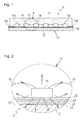
FIG.1 is a sectional view of a mounting substrate according to a first embodiment of the present invention and a light-emitting device including the mounting substrate. -
FIG.2 is an enlarged sectional view of a portion A of the mounting substrate. -
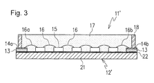
FIG.3 is a sectional view of a mounting substrate according to a second embodiment of the present invention and a light-emitting device including the mounting substrate. - Embodiments of a mounting substrate according to the present invention and a light-emitting device using the mounting substrate will be described hereinafter with reference to the accompanying drawings.
FIG.1 illustrates themounting substrate 12 according to a first embodiment of the present invention and the light-emitting device 11 using themounting substrate 12. The light-emitting device 11 has a configuration in which a plurality ofLED elements 15 are arranged on themounting substrate 12 and the plurality of arrangedLED elements 15 are sealed with a light-transmittingresin 17 in which phosphor is contained. - The
mounting substrate 12 according to the present invention has excellent heat dissipation. This is because the mounting substrate has a structure composed of ametal substrate 21 as a base and asurface layer section 22 formed on themetal substrate 21. In addition, at least a pair of external connectingelectrodes mounting substrate 12. - The plurality of
LED elements 15 arranged on themounting substrate 12 include a pair of element electrodes provided on an upper surface of each of the LED elements, a lower surface of each of the LED elements is mounted on the upper surface of themounting substrate 12 through a transparent insulation adhesive and so on.Adjacent LED elements 15 are connected each other bybonding wires 16, and thebonding wires LED elements 15 positioned at opposite ends are connected to the pair of external connectingelectrodes electrodes LED elements 15 emits by applying a predetermined voltage to each of theLED elements 15. -
FIG.2 is an enlarged view of a portion A inFIG.1 , and illustrates a configuration of thesurface layer section 22 formed on the upper surface of themounting substrate 12. As is clear fromFIG. 2 , in thesurface layer section 22, anoxide film layer 23 is provided on the upper surface of themetal substrate 21 which is the base, and further areflection layer 25 and aprotection film layer 26 are provided on or above abarrier layer 24 formed on theoxide film layer 23. - The
metal substrate 21 is formed by a rectangular aluminum plate having a planar area, on which the plurality ofLED elements 15 is arranged. The aluminum plate has good heat dissipation because it is excellent in heat conductivity, and is excellent in heat resistance. A thickness of the aluminum plate is not limited in particular, but, in an embodiment, it is a degree of about 0.7mm. Note that, it is not limited to the aluminum plate, if a metal material has high heat conductivity, it may be employed. - The
oxide film layer 23 is composed of an alumite layer formed by applying anodization treatment to a surface of the aluminum plate as themetal substrate 21. A condition of the anodization is that the alumite layer is formed on the surface of the aluminum plate and is, in particular, not limited to this, a known technology can be adopted. - In a conventional mounting substrate in which the metal substrate is the base, heat dissipation is secured by placing mounting LED elements or semi-conductor elements on the alumite layer directly or on a reflection layer formed on the alumite layer. However, the present invention is characterized in that the
barrier layer 24 is provided on thealumite layer 23 as the oxide film layer and thereflection layer 25 is provided on thebarrier layer 24. - The
barrier layer 24 prevents thealumite layer 23 from being corroded and deteriorated. In addition, in a case where silver as a light reflection material contained in thereflection layer 25 is diffused by influence of heat, the silver is diffused into thealumite layer 23 to generate insulation breakdown of thealumite layer 23. Thebarrier layer 24 is provided to prevent the insulation breakdown. Thebarrier layer 24 is a uniformly-thick film layer formed on a surface of thealumite layer 23. Thebarrier layer 24 is formed by spattering, evaporation coating, plating and so on with a metal containing at least one of titan, nickel, ruthenium, palladium, tungsten, and platinum. The formation of the uniform thickness of thebarrier layer 24 makes it possible to equally reflect light emitted from theLED elements 15 and equally distribute heat by the emission of light toward themetal substrate 21. In addition, because thebarrier layer 24 itself has light-reflecting effect, a fixed light-reflecting effect can be expected by the diffusion of the silver as the light reflection material. - The
reflection layer 25 is formed to have a fixed thickness by diffusing silver equal to or more than 90% in purity as the light reflection material in a transparent resin and applying it on thebarrier layer 24, in one embodiment. In another embodiment, the reflection layer may be formed by evaporating silver equal to or more than 90% in purity on thebarrier layer 24. The purity of the silver is decided in consideration of light reflecting effect, strength of the evaporated film, affinity with other layers, and so on. The light emitted from theLED elements 15 is reflected upward by thereflection layer 25. Note that the silver used as the light reflection material is an excellent material having high heat conductivity and a high light reflectance, however, materials such as aluminum and so on other than silver having high reflectivity may be used. - The
protection film layer 26 formed on thereflection layer 25 is provided as an insulation protector of a surface of thereflection layer 25. In addition, a coating is thinly formed on thereflection layer 25 by a resin material having a high light-transmitting property such as epoxy resin, acryl resin, silicone resin, fluororesin and so on not to reduce the light reflectance of thereflection layer 25. Theprotection film layer 26 may be configured by forming the evaporated film of titanium oxide or silicon oxide on thereflection layer 25. In addition, a multilayered protection film may be formed by optionally combining the coating of the light-transmitting resin, the evaporated film of titanium oxide, the evaporated film of silicon oxide. By forming the protection film into the multilayer, it is possible to improve the strength of the protection film itself and take measures to a pinhole(s) of the protection film. Note that in a multilayer structure in which the evaporated film the silicon oxide of a low refractive index is formed on the evaporated film of the titanium oxide of a high refractive index, if a film thickness of each layer is thin, the reduction of reflection effect is generated. As a result, it is needed to take consideration such as thickening the thickness of the film even some extent. It is possible to further improve the light reflection effect of thereflection layer 25 by mixing a light diffusing material and so on in the light-transmitting resin. - The mounting
substrate 12 in which thesurface layer section 22 is formed on the surface of themetal substrate 21 can efficiently releases heat generated at the time when the plurality ofLED elements 15 emit light to themetal substrate 21 side. In addition, it is possible to efficiently reflect the light emitted from the plurality ofLED elements 15 to an upper direction of the mountingsubstrate 12 by the reflection effect on thereflection layer 25. In particular, in the present invention, because thebarrier layer 24 is provided on thealumite layer 23 and thereflection layer 25 is provided on thebarrier layer 24, the silver in thereflection layer 25 is not diffused by heat into thealumite layer 23. Therefore, there is no possibility of the direct influence of the diffusion of the silver on themetal substrate 21. As a result, it is possible to hold a stable quality as the light-emitting device 11 throughout a long period without deteriorating characteristics of the mountingsubstrate 12 and the plurality ofLED elements 15 mounted on the mountingsubstrate 12. - It is required that the mounting
substrate 12, at a shipping inspection in the final process of commercialization of product, passes tests such as a continuity test and so on under a high temperature environment in which stress applied on the substrate is larger than that in a case where the product is actually used. Because the stress under such a high temperature is given to the mountingsubstrate 12, in particular, thereflection layer 25 easily receives influence by heat. However, the light reflectance of the reflection layer cannot be reduced because the diffusion of the silver contained in thereflection layer 25 is restrained by thebarrier layer 24 positioned under thereflection layer 25. As a result, it is possible to significantly reduce generation rate of defective products and improve yield. -
FIG.3 illustrates a mounting substrate 12' according to a second embodiment of the present invention and a light-emitting device 11' using the mountingsubstrate 12. In the mounting substrate 12' according to this embodiment, themetal substrate 21 and thesurface layer section 22 formed on the upper surface of themetal substrate 21 have the same configuration as that in the mountingsubstrate 12 according to the previous embodiment. This embodiment differs from the previous embodiment only in that acircuit substrate 13 is provided on thesurface layer section 22 to surround the plurality ofLED elements 15. Therefore, the identical reference numbers are attached to the similar parts, detailed descriptions thereof are omitted. Note that the at least pair of external connectingelectrodes circuit substrate 13. - In the light-emitting device 11' according to the present embodiment, the plurality of
LED elements 15 are arranged on the upper surface of the mounting substrate 12', the adjacent LED elements are connected each other by thebonding wires 16, and thebonding wires LED elements 15 at the opposite ends to the external connectingelectrodes LED elements 15 arranged on the mounting substrate 12' are sealed with the light-transmittingresin 17 containing the phosphor. In addition to this, in the embodiment, the light-transmittingresin 17 is surrounded by a ring-shapedreflection frame 18. It is possible to improve light reflecting effect by forming thereflection frame 18 with a white resin. -
- 11, 11'
- light-emitting device
- 12, 12'
- mounting substrate
- 13
- circuit substrate
- 14a, 14b
- external connecting electrodes
- 15
- LED elements
- 16a, 16b, 16c
- bonding wires
- 17
- light-transmitting resin
- 18
- reflection frame
- 21
- metal substrate
- 22
- surface layer section
- 23
- oxide film layer (alumite layer)
- 24
- barrier layer
- 25
- reflection layer
- 26
- protection film layer
Claims (13)
- A mounting substrate comprising:a metal substrate; anda surface layer section formed on an upper surface of the metal substrate,wherein the surface layer section includes
an oxide film layer formed on a surface of the metal substrate,
a barrier layer formed on the oxide film layer,
a reflection layer formed on the barrier layer and containing a light-reflecting material, and
a protection film layer formed on the reflection layer. - The mounting substrate according to claim 1, wherein
the metal substrate is formed by an aluminum plate, and
the oxide film layer is formed by an alumite layer formed on a surface of the aluminum plate. - The mounting substrate according to claim 1, wherein
the barrier layer contains at least one of titan, nickel, ruthenium, palladium, tungsten, and platinum. - The mounting substrate according to claim 1, wherein
the barrier layer is formed on the oxide film layer to have a uniform thickness. - The mounting substrate according to claim 1, wherein
the reflection layer is formed by a resin film in which silver is contained in a light-transmitting resin. - The mounting substrate according to claim 1, wherein
the reflection layer is formed by an evaporated film of silver. - The mounting substrate according to claim 5 or 6, wherein
the silver is 90% or more in purity. - The mounting substrate according to claim 1, wherein
the protection film layer is formed by a light-transmitting resin film. - The mounting substrate according to claim 1, wherein
the protection film layer is formed by an evaporated film of titanium oxide or an evaporated film of silicon oxide. - The mounting substrate according to claim 1, wherein
the protection film layer is formed by a multilayer film in which a light-transmitting resin film, an evaporated film of titanium oxide, and an evaporated film of silicon oxide are adequately combined. - The mounting substrate according to claim 1, wherein
a wiring substrate on which a wiring pattern is formed is provided on end portions of an upper surface of the surface layer section. - A light-emitting device comprising:the mounting substrate claimed in claim 1;at least one light-emitting diode element mounted on a surface of the mounting substrate; anda light-transmitting resin body that seals the light-emitting diode element.
- The light-emitting device according to claim 12, wherein
the light-transmitting resin is surrounded by a frame.
Applications Claiming Priority (2)
| Application Number | Priority Date | Filing Date | Title |
|---|---|---|---|
| JP2012258102 | 2012-11-27 | ||
| PCT/JP2013/001685 WO2014083714A1 (en) | 2012-11-27 | 2013-03-14 | Mounting substrate and light emitting apparatus using mounting substrate |
Publications (2)
| Publication Number | Publication Date |
|---|---|
| EP2927971A1 true EP2927971A1 (en) | 2015-10-07 |
| EP2927971A4 EP2927971A4 (en) | 2015-12-02 |
Family
ID=50827382
Family Applications (1)
| Application Number | Title | Priority Date | Filing Date |
|---|---|---|---|
| EP13858852.0A Withdrawn EP2927971A4 (en) | 2012-11-27 | 2013-03-14 | MOUNTING SUBSTRATE AND LIGHT EMITTING APPARATUS USING MOUNTING SUBSTRATE |
Country Status (5)
| Country | Link |
|---|---|
| US (1) | US9368707B2 (en) |
| EP (1) | EP2927971A4 (en) |
| JP (1) | JPWO2014083714A1 (en) |
| CN (1) | CN104813493A (en) |
| WO (1) | WO2014083714A1 (en) |
Cited By (2)
| Publication number | Priority date | Publication date | Assignee | Title |
|---|---|---|---|---|
| WO2018164870A1 (en) * | 2017-03-08 | 2018-09-13 | Cree, Inc. | Substrates for light emitting diodes and related methods |
| WO2022090035A1 (en) | 2020-10-29 | 2022-05-05 | Signify Holding B.V. | Insulating metal pcb with light-blocking layer |
Families Citing this family (5)
| Publication number | Priority date | Publication date | Assignee | Title |
|---|---|---|---|---|
| JP6381327B2 (en) | 2014-07-17 | 2018-08-29 | シチズン電子株式会社 | LED light emitting device and manufacturing method thereof |
| JP6817599B2 (en) * | 2016-03-10 | 2021-01-20 | パナソニックIpマネジメント株式会社 | LED module |
| JP2017163058A (en) * | 2016-03-10 | 2017-09-14 | パナソニックIpマネジメント株式会社 | LED module |
| CN108878627B (en) * | 2017-05-09 | 2020-05-01 | 中国科学院化学研究所 | LED substrate, preparation method and application thereof |
| JP7085894B2 (en) * | 2018-05-17 | 2022-06-17 | スタンレー電気株式会社 | Light transmission plate with light emitting function and its manufacturing method |
Family Cites Families (23)
| Publication number | Priority date | Publication date | Assignee | Title |
|---|---|---|---|---|
| JPS55132083A (en) * | 1979-03-30 | 1980-10-14 | Sanyo Electric Co Ltd | Light emitting diode substrate |
| JPH11342648A (en) * | 1998-05-29 | 1999-12-14 | Canon Inc | LED exposure head |
| JP2007067116A (en) | 2005-08-30 | 2007-03-15 | Toshiba Lighting & Technology Corp | Light emitting device |
| JP5066333B2 (en) * | 2005-11-02 | 2012-11-07 | シチズン電子株式会社 | LED light emitting device. |
| JP2007194385A (en) | 2006-01-19 | 2007-08-02 | Stanley Electric Co Ltd | Semiconductor light emitting device and method for manufacturing semiconductor light emitting device |
| KR100764388B1 (en) * | 2006-03-17 | 2007-10-05 | 삼성전기주식회사 | Anodized Metal Substrate Module |
| JP5179766B2 (en) * | 2007-03-08 | 2013-04-10 | スタンレー電気株式会社 | Semiconductor light emitting device and manufacturing method thereof |
| JP2009258546A (en) * | 2008-04-21 | 2009-11-05 | Hitachi Displays Ltd | Liquid crystal display device |
| JP5345363B2 (en) | 2008-06-24 | 2013-11-20 | シャープ株式会社 | Light emitting device |
| JP2008263248A (en) * | 2008-08-07 | 2008-10-30 | Sumitomo Electric Ind Ltd | Semiconductor light emitting element mounting member and manufacturing method thereof |
| US8188486B2 (en) * | 2008-09-16 | 2012-05-29 | Osram Sylvania Inc. | Optical disk for lighting module |
| KR101077264B1 (en) * | 2009-02-17 | 2011-10-27 | (주)포인트엔지니어링 | Substrate for optical device, optical device package having the same and menufacturing method thereof |
| JP5322801B2 (en) * | 2009-06-19 | 2013-10-23 | スタンレー電気株式会社 | Semiconductor light emitting device and manufacturing method thereof |
| JP5617210B2 (en) | 2009-09-14 | 2014-11-05 | デクセリアルズ株式会社 | Light-reflective anisotropic conductive adhesive and light-emitting device |
| TWI499099B (en) * | 2009-12-30 | 2015-09-01 | 晶元光電股份有限公司 | Semiconductor light-emitting element with protective layer |
| JP5429038B2 (en) * | 2010-05-14 | 2014-02-26 | 旭硝子株式会社 | Light emitting element mounting substrate and light emitting device |
| JP5720454B2 (en) | 2010-07-26 | 2015-05-20 | 旭硝子株式会社 | Light-emitting element mounting substrate, method for manufacturing the same, and light-emitting device |
| CN102347426A (en) | 2010-07-26 | 2012-02-08 | 旭硝子株式会社 | Substrate for mounting light-emitting element, production process thereof and light-emitting device |
| TW201214793A (en) * | 2010-07-26 | 2012-04-01 | Asahi Glass Co Ltd | Substrate for mounting light emitting element, method for manufacturing the same and light emitting device |
| JP5583051B2 (en) * | 2011-02-23 | 2014-09-03 | 京セラ株式会社 | Light emitting element mounting substrate and light emitting device |
| DE202011050976U1 (en) * | 2011-08-12 | 2012-11-15 | Alanod Aluminium-Veredlung Gmbh & Co. Kg | Highly reflective substrate for light-emitting diodes and light-emitting device with such a carrier material |
| JP6366337B2 (en) * | 2014-04-23 | 2018-08-01 | シチズン電子株式会社 | LED light emitting device and manufacturing method thereof |
| JP6381327B2 (en) * | 2014-07-17 | 2018-08-29 | シチズン電子株式会社 | LED light emitting device and manufacturing method thereof |
-
2013
- 2013-03-14 EP EP13858852.0A patent/EP2927971A4/en not_active Withdrawn
- 2013-03-14 JP JP2014549755A patent/JPWO2014083714A1/en active Pending
- 2013-03-14 US US14/647,161 patent/US9368707B2/en active Active
- 2013-03-14 WO PCT/JP2013/001685 patent/WO2014083714A1/en not_active Ceased
- 2013-03-14 CN CN201380061994.1A patent/CN104813493A/en active Pending
Cited By (3)
| Publication number | Priority date | Publication date | Assignee | Title |
|---|---|---|---|---|
| WO2018164870A1 (en) * | 2017-03-08 | 2018-09-13 | Cree, Inc. | Substrates for light emitting diodes and related methods |
| US10439114B2 (en) | 2017-03-08 | 2019-10-08 | Cree, Inc. | Substrates for light emitting diodes and related methods |
| WO2022090035A1 (en) | 2020-10-29 | 2022-05-05 | Signify Holding B.V. | Insulating metal pcb with light-blocking layer |
Also Published As
| Publication number | Publication date |
|---|---|
| EP2927971A4 (en) | 2015-12-02 |
| US9368707B2 (en) | 2016-06-14 |
| US20150325761A1 (en) | 2015-11-12 |
| WO2014083714A1 (en) | 2014-06-05 |
| CN104813493A (en) | 2015-07-29 |
| JPWO2014083714A1 (en) | 2017-01-05 |
Similar Documents
| Publication | Publication Date | Title |
|---|---|---|
| US9368707B2 (en) | Mounting substrate and light-emitting device using the same | |
| US10910536B2 (en) | Light emitting element | |
| RU2596221C2 (en) | Module of light source circuit, illuminator and display | |
| US9070831B2 (en) | Light-emitting device each having variable distances between pairs of electrode pads with respect to Zener diodes and lighting apparatus using the same | |
| JP5885922B2 (en) | Light emitting device | |
| US20120218737A1 (en) | Lighting apparatus | |
| US10553770B2 (en) | Light emitting device including light emitting element with multiple light emitting cells | |
| WO2009116457A1 (en) | Wiring board for mounting light emitting element thereon, and light emitting device | |
| JP2012256908A (en) | Light-emitting module, light source device, liquid crystal display device, and manufacturing method for light-emitting module | |
| US20150280093A1 (en) | Light emitting device, method for manufacturing same, and body having light emitting device mounted thereon | |
| US9577153B2 (en) | Light emission device and illumination device | |
| US20140361324A1 (en) | Semiconductor light emitting device | |
| US20140334164A1 (en) | Wiring board and light emitting device using same | |
| JP5817297B2 (en) | Light emitting device and lighting device | |
| US8902382B2 (en) | Light emitting diode element, light source device, surface light source illumination device, and liquid crystal display device | |
| JP5638922B2 (en) | Light emitting device and lighting device including light emitting device | |
| KR20190035527A (en) | Light emitting device and light emitting apparatus | |
| US9429305B2 (en) | Light emitting device | |
| KR102509061B1 (en) | Light emitting device package | |
| US20160260880A1 (en) | Light-emitting device using mounting substrate | |
| JP6179857B2 (en) | Light emitting device | |
| JP2018093097A (en) | Light-emitting device | |
| TW202327132A (en) | Light-emitting module | |
| US11335840B2 (en) | Optical semiconductor device package, optical semiconductor device, and manufacturing method for optical semiconductor device package | |
| JP6135199B2 (en) | Light emitting device |
Legal Events
| Date | Code | Title | Description |
|---|---|---|---|
| PUAI | Public reference made under article 153(3) epc to a published international application that has entered the european phase |
Free format text: ORIGINAL CODE: 0009012 |
|
| 17P | Request for examination filed |
Effective date: 20150626 |
|
| AK | Designated contracting states |
Kind code of ref document: A1 Designated state(s): AL AT BE BG CH CY CZ DE DK EE ES FI FR GB GR HR HU IE IS IT LI LT LU LV MC MK MT NL NO PL PT RO RS SE SI SK SM TR |
|
| AX | Request for extension of the european patent |
Extension state: BA ME |
|
| RA4 | Supplementary search report drawn up and despatched (corrected) |
Effective date: 20151103 |
|
| RIC1 | Information provided on ipc code assigned before grant |
Ipc: H01L 33/64 20100101AFI20151028BHEP Ipc: H01L 33/60 20100101ALI20151028BHEP Ipc: H01L 23/12 20060101ALI20151028BHEP |
|
| DAX | Request for extension of the european patent (deleted) | ||
| RAP1 | Party data changed (applicant data changed or rights of an application transferred) |
Owner name: CITIZEN WATCH CO., LTD. Owner name: CITIZEN ELECTRONICS CO., LTD. |
|
| 17Q | First examination report despatched |
Effective date: 20200107 |
|
| STAA | Information on the status of an ep patent application or granted ep patent |
Free format text: STATUS: THE APPLICATION HAS BEEN WITHDRAWN |
|
| 18W | Application withdrawn |
Effective date: 20200416 |