EP2927938B1 - Method of etching - Google Patents
Method of etching Download PDFInfo
- Publication number
- EP2927938B1 EP2927938B1 EP15162490.5A EP15162490A EP2927938B1 EP 2927938 B1 EP2927938 B1 EP 2927938B1 EP 15162490 A EP15162490 A EP 15162490A EP 2927938 B1 EP2927938 B1 EP 2927938B1
- Authority
- EP
- European Patent Office
- Prior art keywords
- etch
- bias power
- etch step
- etching
- silicon
- Prior art date
- Legal status (The legal status is an assumption and is not a legal conclusion. Google has not performed a legal analysis and makes no representation as to the accuracy of the status listed.)
- Active
Links
Images


Classifications
-
- H—ELECTRICITY
- H10—SEMICONDUCTOR DEVICES; ELECTRIC SOLID-STATE DEVICES NOT OTHERWISE PROVIDED FOR
- H10W—GENERIC PACKAGES, INTERCONNECTIONS, CONNECTORS OR OTHER CONSTRUCTIONAL DETAILS OF DEVICES COVERED BY CLASS H10
- H10W20/00—Interconnections in chips, wafers or substrates
- H10W20/01—Manufacture or treatment
- H10W20/021—Manufacture or treatment of interconnections within wafers or substrates
- H10W20/023—Manufacture or treatment of interconnections within wafers or substrates the interconnections being through-semiconductor vias
-
- H—ELECTRICITY
- H01—ELECTRIC ELEMENTS
- H01J—ELECTRIC DISCHARGE TUBES OR DISCHARGE LAMPS
- H01J37/00—Discharge tubes with provision for introducing objects or material to be exposed to the discharge, e.g. for the purpose of examination or processing thereof
- H01J37/32—Gas-filled discharge tubes
- H01J37/32009—Arrangements for generation of plasma specially adapted for examination or treatment of objects, e.g. plasma sources
- H01J37/32082—Radio frequency generated discharge
- H01J37/321—Radio frequency generated discharge the radio frequency energy being inductively coupled to the plasma
-
- H—ELECTRICITY
- H01—ELECTRIC ELEMENTS
- H01J—ELECTRIC DISCHARGE TUBES OR DISCHARGE LAMPS
- H01J37/00—Discharge tubes with provision for introducing objects or material to be exposed to the discharge, e.g. for the purpose of examination or processing thereof
- H01J37/32—Gas-filled discharge tubes
- H01J37/32431—Constructional details of the reactor
- H01J37/32697—Electrostatic control
- H01J37/32706—Polarising the substrate
-
- H—ELECTRICITY
- H01—ELECTRIC ELEMENTS
- H01J—ELECTRIC DISCHARGE TUBES OR DISCHARGE LAMPS
- H01J37/00—Discharge tubes with provision for introducing objects or material to be exposed to the discharge, e.g. for the purpose of examination or processing thereof
- H01J37/32—Gas-filled discharge tubes
- H01J37/32431—Constructional details of the reactor
- H01J37/32715—Workpiece holder
-
- H—ELECTRICITY
- H10—SEMICONDUCTOR DEVICES; ELECTRIC SOLID-STATE DEVICES NOT OTHERWISE PROVIDED FOR
- H10P—GENERIC PROCESSES OR APPARATUS FOR THE MANUFACTURE OR TREATMENT OF DEVICES COVERED BY CLASS H10
- H10P50/00—Etching of wafers, substrates or parts of devices
- H10P50/20—Dry etching; Plasma etching; Reactive-ion etching
- H10P50/24—Dry etching; Plasma etching; Reactive-ion etching of semiconductor materials
- H10P50/242—Dry etching; Plasma etching; Reactive-ion etching of semiconductor materials of Group IV materials
-
- H—ELECTRICITY
- H10—SEMICONDUCTOR DEVICES; ELECTRIC SOLID-STATE DEVICES NOT OTHERWISE PROVIDED FOR
- H10P—GENERIC PROCESSES OR APPARATUS FOR THE MANUFACTURE OR TREATMENT OF DEVICES COVERED BY CLASS H10
- H10P72/00—Handling or holding of wafers, substrates or devices during manufacture or treatment thereof
- H10P72/04—Apparatus for manufacture or treatment
-
- H—ELECTRICITY
- H10—SEMICONDUCTOR DEVICES; ELECTRIC SOLID-STATE DEVICES NOT OTHERWISE PROVIDED FOR
- H10P—GENERIC PROCESSES OR APPARATUS FOR THE MANUFACTURE OR TREATMENT OF DEVICES COVERED BY CLASS H10
- H10P72/00—Handling or holding of wafers, substrates or devices during manufacture or treatment thereof
- H10P72/04—Apparatus for manufacture or treatment
- H10P72/0402—Apparatus for fluid treatment
- H10P72/0418—Apparatus for fluid treatment for etching
- H10P72/0421—Apparatus for fluid treatment for etching for drying etching
-
- H—ELECTRICITY
- H10—SEMICONDUCTOR DEVICES; ELECTRIC SOLID-STATE DEVICES NOT OTHERWISE PROVIDED FOR
- H10W—GENERIC PACKAGES, INTERCONNECTIONS, CONNECTORS OR OTHER CONSTRUCTIONAL DETAILS OF DEVICES COVERED BY CLASS H10
- H10W20/00—Interconnections in chips, wafers or substrates
- H10W20/01—Manufacture or treatment
- H10W20/021—Manufacture or treatment of interconnections within wafers or substrates
- H10W20/023—Manufacture or treatment of interconnections within wafers or substrates the interconnections being through-semiconductor vias
- H10W20/0245—Manufacture or treatment of interconnections within wafers or substrates the interconnections being through-semiconductor vias comprising use of blind vias during the manufacture
-
- H—ELECTRICITY
- H10—SEMICONDUCTOR DEVICES; ELECTRIC SOLID-STATE DEVICES NOT OTHERWISE PROVIDED FOR
- H10W—GENERIC PACKAGES, INTERCONNECTIONS, CONNECTORS OR OTHER CONSTRUCTIONAL DETAILS OF DEVICES COVERED BY CLASS H10
- H10W20/00—Interconnections in chips, wafers or substrates
- H10W20/01—Manufacture or treatment
- H10W20/021—Manufacture or treatment of interconnections within wafers or substrates
- H10W20/023—Manufacture or treatment of interconnections within wafers or substrates the interconnections being through-semiconductor vias
- H10W20/0249—Manufacture or treatment of interconnections within wafers or substrates the interconnections being through-semiconductor vias wherein the through-semiconductor via protrudes from backsides of the chips, wafers or substrates during the manufacture
-
- H—ELECTRICITY
- H10—SEMICONDUCTOR DEVICES; ELECTRIC SOLID-STATE DEVICES NOT OTHERWISE PROVIDED FOR
- H10P—GENERIC PROCESSES OR APPARATUS FOR THE MANUFACTURE OR TREATMENT OF DEVICES COVERED BY CLASS H10
- H10P74/00—Testing or measuring during manufacture or treatment of wafers, substrates or devices
- H10P74/20—Testing or measuring during manufacture or treatment of wafers, substrates or devices characterised by the properties tested or measured, e.g. structural or electrical properties
- H10P74/203—Structural properties, e.g. testing or measuring thicknesses, line widths, warpage, bond strengths or physical defects
-
- H—ELECTRICITY
- H10—SEMICONDUCTOR DEVICES; ELECTRIC SOLID-STATE DEVICES NOT OTHERWISE PROVIDED FOR
- H10P—GENERIC PROCESSES OR APPARATUS FOR THE MANUFACTURE OR TREATMENT OF DEVICES COVERED BY CLASS H10
- H10P74/00—Testing or measuring during manufacture or treatment of wafers, substrates or devices
- H10P74/23—Testing or measuring during manufacture or treatment of wafers, substrates or devices characterised by multiple measurements, corrections, marking or sorting processes
- H10P74/238—Testing or measuring during manufacture or treatment of wafers, substrates or devices characterised by multiple measurements, corrections, marking or sorting processes comprising acting in response to an ongoing measurement without interruption of processing, e.g. endpoint detection or in-situ thickness measurement
Definitions
- This invention relates to methods of etching a semiconductor substrate, to reveal one or more features buried in the substrate such as vias.
- TSV Through Silicon Vias
- TSVs are vertical electrical connections typically filled with copper which extend vertically through silicon wafers.
- TSVs are important components in the creation of 3D packages and 3D integrated circuits.
- the electrically conductive via material is protected with an outer liner formed from a suitable protective material such as a siliconoxide.
- the TSVs, including the protective layers are initially buried within a silicon substrate.
- Via reveal etching involves etching the silicon substrate so as to reveal the upper tips of the TSVs. To achieve optimal results with a via reveal etch, it is considered necessary to satisfy three criteria. Firstly, the etch should achieve a high etch rate with good uniformity.
- the oxide protective liner on the TSV it is necessary to achieve a high silicon to oxide etch selectivity in order to maintain the oxide protective liner on the TSV. This prevents exposure of the underlying electrically conducted material (such as copper) to the process gases and plasma which are ubiquitously used to achieve the etch.
- the final silicon surface achieved at the end of the etch process should be as smooth as possible. It is necessary to achieve a smooth surface in order to prevent problems in subsequent steps of the manufacturing process, for example optical inspection failures due to the wafer having unacceptable properties of reflection, alignment problems, and problems associated with laser dicing. In practice, there is a fine balance between surface roughness and etch selectivity.
- processes and process parameters which can result in good selectivity can also result in a high level of surface roughness.
- the reverse is also true.
- it is known that the use of a high bias power during plasma etching can achieve low silicon roughness levels; however, this results in poor oxide selectivity. It is particularly difficult to balance these different criteria in a continuous process.
- continuous processes are desirable in terms of efficiency.
- a further problem is that surface roughness increases with the depth of silicon removed.
- the present invention in at least some of its embodiments, addresses the above described problems and needs.
- the invention is particularly useful in TSV reveal etching, it has utility more generally in semiconductor etching processes.
- a to B selectivity expressed herein as a ratio is understood to refer to the ratio of the etch rate of A to the etch rate of B.
- a silicon to silicon dioxide selectivity of greater than 150:1 means that the etch rate of silicon is greater than 150 times the etch rate of silicon dioxide.
- a method of etching a semiconductor substrate to reveal one or more features buried in the substrate including the steps of:
- the method is compatible with high etch rate processes and with continuous operation.
- the method can be advantageous when it is desirable to balance one process parameter or property against another.
- the method is particularly applicable when it is desirable to balance etch selectivity for the semiconductor substrate and the features against post-etch surface morphology, for example surface roughness.
- the bias power may be pulsed during the first etch step.
- the bias power may be pulsed with a duty cycle in the range 10 to 50%.
- a bias power of 250W or more may be used when the bias power is pulsed.
- the bias power may be applied to the substrate continuously during the first etch step.
- a bias power of 75W or more may be used when the bias power is applied continuously.
- the second etch step may be a plasma etch step. It is believed that the use of a plasma to perform a second etch step is likely to be the most acceptable from a commercial point of view.
- the bias power or powers are RF powers.
- the semiconductor substrate is positioned on a substrate support and an RF signal is applied to a substrate support in order to produce the electrical bias.
- the features may include an outer protective layer.
- the outer protective layer may be an oxide layer.
- the features may be vias.
- the features may be TSVs.
- the vias may include outer protective layers such as an oxide layer.
- the oxide layer may be SiO 2 Silicon dioxide may be deposited by CVD (chemical vapour deposition) such as LPCVD (low pressure CVD) or PECVD (plasma enhanced CVD). Other materials, such as low k SiOC or SiOF, might be used.
- the TSVs may each include an outer protective layer of silicon dioxide.
- the semiconductor substrate may be silicon.
- the second etch step may be performed either without a bias power or with a bias power which is lower than the bias power applied during the first etch step so as to produce a silicon to silicon dioxide selectivity of greater than 100:1, preferably greater than 150:1.
- the first and second etch steps may be alternately repeated to produce a surface roughness Ra as measured by atomic force microscopy of 2nm or less, preferably 1nm or less.
- the semiconductor substrate may be silicon. However, the invention can be applied to other semiconductor materials.
- the first and second steps may be alternately repeated at least ten times.
- the skilled reader will appreciate that the number of times the first and second steps are alternately repeated (the number of cycles) can be any number suitable to achieve the required process end point. In particular, there is no particular upper limit to the number of cycles.
- the first and second etch steps may each be performed for a time in the range 0.5 to 10 seconds.
- the use of relatively short time periods for the etch steps can be beneficial. For example, surface roughness may be significantly reduced and etch selectivity may be increased.
- the first etch step and, optionally, the second etch step may be performed using a plasma formed using a fluorine containing gas.
- the fluorine containing gas may be SF 6 or a mixture of etching gases including SF 6 .
- the first etch step may be performed with a bias power which is high enough to achieve an acceptably low degree of surface roughness.
- the second etch step may be performed with a bias power which is lower than the bias power used in the first etch step in order to provide improved selectivity for etching the semiconductor substrate in relation to etching of the features.
- the bias power may be 50V or less. However, it is preferred that no bias power is applied in order to achieve improved etch selectivity.
- a plurality of process parameters are associated with the first and second etch steps.
- the process parameters may be altered during the course of the etching.
- the process parameters may be altered when a process condition is detected.
- the process condition detected may be the revealing of the features.
- the process condition detected may be the revealing of the upper portion or portions of one or more TSVs.
- the order of the first and second steps is not critical, in terms of whether the method commences with the first etch step or the second etch step.
- Bias power may be applied during both the first and second etch steps.
- bias power is pulsed during one etch step and applied continuously during the other etch step.
- the time averaged power during each etch step, rather than the peak power during a pulse which may be used to consider which bias power is lower than the other.
- the invention provides etching of semiconductors in a cyclic process.
- the etching alternates between a step in which a plasma etch is performed using a bias power, and a second etch step in which there is no bias power, or a lower bias power is used.
- the invention will now be exemplified in connection with TSV reveal etching. However, the invention can be utilised in other etching applications.
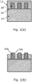
- FIG 1 shows a TSV reveal silicon etch process.
- Figure 1(a) shows TSVs 10 buried within a silicon wafer 12 prior to etching.
- the silicon wafer 12 is bonded to a carrier wafer 14 by an adhesive layer 16.
- the carrier wafer 14 can be of any suitable material such as silicon or glass.
- Etching is performed to reveal the TSVs 10, as shown in Figure 1(b) .
- each TSV 10 comprises an electrically conductive material 10a which is coated with a protective oxide liner 10b.
- the electrically conductive material is generally a metal, such as copper. It is important that there is no exposure of the underlying electrically conductive material 10b to the harsh conditions of the plasma. This in turn places a process requirement that the etching proceeds with a high silicon to oxide selectivity.
- FIG. 2 shows an etching apparatus, depicted generally at 20, which may be used to perform etching of the invention.
- a primary gas feed 22 enters a primary chamber 24 which has an associated primary ionisation source 26.
- An RF antenna 28 acts as an ICP source. This can be assisted by a DC coil 30 to modify the confinement of the plasma produced.
- a Faraday shield 38 can be provided between the DC coil 30 and the wall of the primary chamber 24 to reduce capacitive coupling.
- the plasma from the primary source enters a main chamber 32 where a wafer 34 to be processed is placed on a wafer support platen 36, which in this embodiment is an electrostatic chuck. A pressure of helium is applied to the underside of the electrostatic chuck for cooling purposes.
- the main chamber 32 has a secondary ionisation source 40 having a secondary RF coil 42 placed around the main chamber 32 to provide a secondary plasma close to the chamber wall.
- the RF coil 30 operates at any convenient frequency, typically 13.56MHz.
- the RF coil 42 could also operate at 13.56MHz, or at a lower frequency such as 1-2MHz.
- An annular gas distribution system 44 is incorporated into the main chamber 32 to provide an independent gas source for the secondary plasma.
- the edge of the wafer 34 may be protected by a wafer edge protection (WEP) device 46.
- the apparatus is pumped through a gate valve 48 by a turbo pump 50.
- a bias RF source 52 is used to supply an RF signal to the wafer support 26.
- Etching apparatus of this type having two RF coils to produce two plasmas, are produced commercially by the applicant under the trade name Pegasus (RTM).
- RTM Pegasus
- the skilled reader will appreciate that the invention is in no way limited to twin RF coil apparatus of this type. In fact, the invention can be implemented over a wide range of plasma etching apparatus.
- the invention provides cyclic etching in which first and second etch steps are alternately repeated.
- a bias power is applied to the wafer support 36 by the RF source 52.
- the bias power can be applied continuously during the first etch step, in which instance power of around 100W has been found to be suitable. However, it is preferred that the bias power is pulsed during the first etch step. For pulsed bias power, a power of 500W pulsed with a 20% duty cycle has been found to be suitable.
- the second etch step it is preferred that no RF bias power is applied.
- the length of each of the first and second etch steps can be selected according to the specific application envisaged. In general, each of the first and second etch steps are performed for a time in the range 0.5 to 10 seconds.
- Typical periods are 3 seconds for each first etch step and 6 seconds for each second etch step, at least at the beginning of the process.
- the total number of cycles depends upon the etch rate and the target depth.
- the total number of cycles required can be either predetermined or controlled according to the progress of the etching process.
- Table 1c) shows an example of process conditions utilised.
- Table 1 a) and b) show process conditions which were used to produce comparative data Table 1.
- Step Name (units) Etch 1 Etch 2 Step Time (Sec) 3 6 Loop Num 20 Pressure (Torr) 85 85 Platen Power (Watts) 500 0 Platen Mod Duty % 20 20 Source Power (Watts) 4000 4000 Secondary Power (Watts) 3750 3750 Primary SF6 (sccm) 1000 1000 Secondary SF6 (sccm) 400 400 He Pressure (Torr) 15 15
- the source powers, gas flows, and pressure all remain the same between cycles.
- these parameters could be different between the first etch step and the second etch step and/or they could change over the total time of the etching process.
- the length of time of the first etch and/second etch steps could be varied as the etching process proceeds.
- the bias power could also be varied as the etching process proceeds.
- the process conditions shown in Table 1 result in a high etch rate (greater than 8.5 microns/min). Whilst it is advantageous that the invention can be applied to high etch rate processes of this type, it can also be applied to etch processes which use lower power and gas flows.
- Figure 3 shows SEM images which indicate how the cyclical process of the invention improves surface roughness. Silicon wafers were etched at ⁇ 9 micron/min for 180 seconds to remove ⁇ 27micron of silicon. In processes 1a) & 1b) there is a short 30sec "break through" BT1 step prior to the bulk etch. This is not required in the process 1c). This short step removes the discontinuity at the wafer surface and is widely used when plasma etching thin films.
- Figure 3(a) shows an SEM image of silicon etched a low bias process (Table 1a) conditions) which should maximise selectivity between the Si and SiO 2 etch rates.
- Figure 3(b) shows an SEM image of silicon etched using a continuous bias of 100W throughout the etching. As expected, a significantly improved degree of surface roughness is observed. Process conditions for this wafer can be seen in Table 1b). However, as explained in more detail below, the use of this etching process results in unacceptably poor silicon to oxide selectivity.
- Figure 3(c) shows an SEM image of silicon etched according to the cyclic process of the invention using the process conditions described in Table 1c. It can be seen that an excellent surface is obtained, with a low degree of roughness. No visible artefacts can be observed. This is confirmed by AFM data shown in Figure 4.
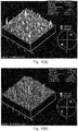
- Figure 4(a) shows AFM data obtained after a typical prior art process. A surface roughness value Ra of 5.9nm is observed by using the high selectivity process described in Table 1a).
- Figure 4(b) shows AFM data obtained when analysing silicon etched using the process conditions of Table 1c. A smooth surface profile is observed, with a measured roughness Ra of 0.97nm.
- the invention can be combined with end-point detection systems which detect when the tip of the vias are revealed.
- An end-point detection system of this type is disclosed in the Applicant's earlier European patent application 12192364.3.
- This end-point detection system can be combined with the present invention.
- the end-point detection system records the time of the via tip reveal.
- the detection of the via tip reveal is used to trigger an adjustment of the process parameters. Additionally or alternatively, a defined number of cycles can be performed after the tip is revealed in order to achieved a desired exposure height of the via above the final surface of the semiconductor.
Landscapes
- Physics & Mathematics (AREA)
- Engineering & Computer Science (AREA)
- Plasma & Fusion (AREA)
- Chemical & Material Sciences (AREA)
- Analytical Chemistry (AREA)
- Drying Of Semiconductors (AREA)
Description
- This invention relates to methods of etching a semiconductor substrate, to reveal one or more features buried in the substrate such as vias.
- Through Silicon Vias (TSV) are vertical electrical connections typically filled with copper which extend vertically through silicon wafers. TSVs are important components in the creation of 3D packages and 3D integrated circuits. During the manufacturing process, it is typical for the electrically conductive via material to be protected with an outer liner formed from a suitable protective material such as a siliconoxide. In the manufacturing process, the TSVs, including the protective layers, are initially buried within a silicon substrate. Via reveal etching involves etching the silicon substrate so as to reveal the upper tips of the TSVs. To achieve optimal results with a via reveal etch, it is considered necessary to satisfy three criteria. Firstly, the etch should achieve a high etch rate with good uniformity. Secondly, it is necessary to achieve a high silicon to oxide etch selectivity in order to maintain the oxide protective liner on the TSV. This prevents exposure of the underlying electrically conducted material (such as copper) to the process gases and plasma which are ubiquitously used to achieve the etch. A silicon to oxide selectivity of greater than 100:1, and preferably greater than 150:1, is considered desirable for this purpose. Thirdly, the final silicon surface achieved at the end of the etch process should be as smooth as possible. It is necessary to achieve a smooth surface in order to prevent problems in subsequent steps of the manufacturing process, for example optical inspection failures due to the wafer having unacceptable properties of reflection, alignment problems, and problems associated with laser dicing. In practice, there is a fine balance between surface roughness and etch selectivity. More specifically, processes and process parameters which can result in good selectivity can also result in a high level of surface roughness. The reverse is also true. For example, it is known that the use of a high bias power during plasma etching can achieve low silicon roughness levels; however, this results in poor oxide selectivity. It is particularly difficult to balance these different criteria in a continuous process. However, continuous processes are desirable in terms of efficiency. A further problem is that surface roughness increases with the depth of silicon removed.
- The present invention, in at least some of its embodiments, addresses the above described problems and needs. Although the invention is particularly useful in TSV reveal etching, it has utility more generally in semiconductor etching processes.
- D. Thomas et al ("Plasma etch and low temperature PECVD process for via reveal applications", Electronic Components and Technology Conference (ECTC), 2012 IEEE 62nd, IEEE, 29 May 2012, pp1662-1667) describes single step and two step approaches to via reveal etching.
- For the avoidance of doubt, the term "A to B selectivity" expressed herein as a ratio is understood to refer to the ratio of the etch rate of A to the etch rate of B. For example, a silicon to silicon dioxide selectivity of greater than 150:1 means that the etch rate of silicon is greater than 150 times the etch rate of silicon dioxide.
- According to the invention there is provided a method of etching a semiconductor substrate to reveal one or more features buried in the substrate, the method including the steps of:
- performing a first etch step of etching the substrate using a plasma in which a bias power is applied to the substrate to produce an electrical bias;
- performing a second etch step of etching the substrate without bias power applied to the substrate or with a bias power which is lower than the bias power applied during the first etch step; and alternately repeating the first and second etch steps.
- The method is compatible with high etch rate processes and with continuous operation. The method can be advantageous when it is desirable to balance one process parameter or property against another. The method is particularly applicable when it is desirable to balance etch selectivity for the semiconductor substrate and the features against post-etch surface morphology, for example surface roughness.
- The bias power may be pulsed during the first etch step. The bias power may be pulsed with a duty cycle in the
range 10 to 50%. A bias power of 250W or more may be used when the bias power is pulsed. - Alternatively, the bias power may be applied to the substrate continuously during the first etch step. A bias power of 75W or more may be used when the bias power is applied continuously.
- The second etch step may be a plasma etch step. It is believed that the use of a plasma to perform a second etch step is likely to be the most acceptable from a commercial point of view.
- Generally, the bias power or powers are RF powers. Generally, the semiconductor substrate, is positioned on a substrate support and an RF signal is applied to a substrate support in order to produce the electrical bias.
- The features may include an outer protective layer. The outer protective layer may be an oxide layer.
- The features may be vias. The features may be TSVs. The vias may include outer protective layers such as an oxide layer. The oxide layer may be SiO2 Silicon dioxide may be deposited by CVD (chemical vapour deposition) such as LPCVD (low pressure CVD) or PECVD (plasma enhanced CVD). Other materials, such as low k SiOC or SiOF, might be used.
- The TSVs may each include an outer protective layer of silicon dioxide. The semiconductor substrate may be silicon. The second etch step may be performed either without a bias power or with a bias power which is lower than the bias power applied during the first etch step so as to produce a silicon to silicon dioxide selectivity of greater than 100:1, preferably greater than 150:1.
- The first and second etch steps may be alternately repeated to produce a surface roughness Ra as measured by atomic force microscopy of 2nm or less, preferably 1nm or less.
- The semiconductor substrate may be silicon. However, the invention can be applied to other semiconductor materials.
- The first and second steps may be alternately repeated at least ten times. The skilled reader will appreciate that the number of times the first and second steps are alternately repeated (the number of cycles) can be any number suitable to achieve the required process end point. In particular, there is no particular upper limit to the number of cycles.
- The first and second etch steps may each be performed for a time in the range 0.5 to 10 seconds. The use of relatively short time periods for the etch steps can be beneficial. For example, surface roughness may be significantly reduced and etch selectivity may be increased.
- The first etch step and, optionally, the second etch step may be performed using a plasma formed using a fluorine containing gas. The fluorine containing gas may be SF6 or a mixture of etching gases including SF6.
- The first etch step may be performed with a bias power which is high enough to achieve an acceptably low degree of surface roughness.
- The second etch step may be performed with a bias power which is lower than the bias power used in the first etch step in order to provide improved selectivity for etching the semiconductor substrate in relation to etching of the features. In these embodiments, the bias power may be 50V or less. However, it is preferred that no bias power is applied in order to achieve improved etch selectivity.
- Generally, a plurality of process parameters are associated with the first and second etch steps. The process parameters may be altered during the course of the etching. The process parameters may be altered when a process condition is detected. The process condition detected may be the revealing of the features. The process condition detected may be the revealing of the upper portion or portions of one or more TSVs.
- The order of the first and second steps is not critical, in terms of whether the method commences with the first etch step or the second etch step.
- Bias power may be applied during both the first and second etch steps. In some embodiments, bias power is pulsed during one etch step and applied continuously during the other etch step. In these embodiments, the time averaged power during each etch step, rather than the peak power during a pulse, which may be used to consider which bias power is lower than the other.
- Embodiments of methods in accordance with the invention will now be described with reference to the accompanying drawings, in which:-
-
Figure 1 shows (a) buried TSVs prior to etching and (b) exposed TSVs after a via reveal etch; -
Figure 2 shows apparatus suitable for performing the invention; -
Figure 3 shows scanning electron microscopy (SEM) images of silicon etched with (a) a 50W bias for 30 seconds followed by 0W bias; (b) a 100W bias throughout the etch and (c) a cyclic process; and -
Figure 4 shows atomic force microscopy (AFM) data for silicon etched using (a) a typical process and (b) a cyclic process. - The invention provides etching of semiconductors in a cyclic process. The etching alternates between a step in which a plasma etch is performed using a bias power, and a second etch step in which there is no bias power, or a lower bias power is used. The invention will now be exemplified in connection with TSV reveal etching. However, the invention can be utilised in other etching applications.
-
Figure 1 shows a TSV reveal silicon etch process.Figure 1(a) showsTSVs 10 buried within asilicon wafer 12 prior to etching. Thesilicon wafer 12 is bonded to acarrier wafer 14 by anadhesive layer 16. Thecarrier wafer 14 can be of any suitable material such as silicon or glass. Etching is performed to reveal theTSVs 10, as shown inFigure 1(b) . It is noted that eachTSV 10 comprises an electricallyconductive material 10a which is coated with aprotective oxide liner 10b. The electrically conductive material is generally a metal, such as copper. It is important that there is no exposure of the underlying electricallyconductive material 10b to the harsh conditions of the plasma. This in turn places a process requirement that the etching proceeds with a high silicon to oxide selectivity. -
Figure 2 shows an etching apparatus, depicted generally at 20, which may be used to perform etching of the invention. Aprimary gas feed 22 enters aprimary chamber 24 which has an associatedprimary ionisation source 26. AnRF antenna 28 acts as an ICP source. This can be assisted by aDC coil 30 to modify the confinement of the plasma produced. AFaraday shield 38 can be provided between theDC coil 30 and the wall of theprimary chamber 24 to reduce capacitive coupling. The plasma from the primary source enters amain chamber 32 where awafer 34 to be processed is placed on awafer support platen 36, which in this embodiment is an electrostatic chuck. A pressure of helium is applied to the underside of the electrostatic chuck for cooling purposes. Themain chamber 32 has asecondary ionisation source 40 having asecondary RF coil 42 placed around themain chamber 32 to provide a secondary plasma close to the chamber wall. TheRF coil 30 operates at any convenient frequency, typically 13.56MHz. TheRF coil 42 could also operate at 13.56MHz, or at a lower frequency such as 1-2MHz. An annulargas distribution system 44 is incorporated into themain chamber 32 to provide an independent gas source for the secondary plasma. The edge of thewafer 34 may be protected by a wafer edge protection (WEP)device 46. The apparatus is pumped through agate valve 48 by aturbo pump 50. Abias RF source 52 is used to supply an RF signal to thewafer support 26. In this way, a bias power may be applied to the wafer support platen and consequently to thewafer 34. Etching apparatus of this type, having two RF coils to produce two plasmas, are produced commercially by the applicant under the trade name Pegasus (RTM). However, the skilled reader will appreciate that the invention is in no way limited to twin RF coil apparatus of this type. In fact, the invention can be implemented over a wide range of plasma etching apparatus. - The invention provides cyclic etching in which first and second etch steps are alternately repeated. In the first etch step, a bias power is applied to the
wafer support 36 by theRF source 52. The bias power can be applied continuously during the first etch step, in which instance power of around 100W has been found to be suitable. However, it is preferred that the bias power is pulsed during the first etch step. For pulsed bias power, a power of 500W pulsed with a 20% duty cycle has been found to be suitable. In the second etch step, it is preferred that no RF bias power is applied. The length of each of the first and second etch steps can be selected according to the specific application envisaged. In general, each of the first and second etch steps are performed for a time in the range 0.5 to 10 seconds. Typical periods are 3 seconds for each first etch step and 6 seconds for each second etch step, at least at the beginning of the process. The total number of cycles depends upon the etch rate and the target depth. The total number of cycles required can be either predetermined or controlled according to the progress of the etching process. - Table 1c) shows an example of process conditions utilised. Table 1 a) and b) show process conditions which were used to produce comparative data
Table 1. A) 0W bias process (BT1 = "breakthrough" step prior to etch step) Step Name (units) BT1 Etch Step Time (sec) 30 150 Pressure (Torr) 85 85 Platen Power (Watts) 50 0 Source Power (Watts) 4000 4000 Secondary Power (Watts) 3750 3750 Primary gas SF6 (sccm) 1000 1000 Secondary gas SF6 (sccm) 400 400 He Pressure (Torr) 15 15 Table 1b) 100W process (BT1 = "breakthrough"step prior to etch step) Step Name (units) BT1 Etch Step Time (Sec) 30 150 Pressure (Torr) 85 85 Platen Power (Watts) 100 100 Source Power (Watts) 4000 4000 Secondary Power (Watts) 3750 3750 Primary SF6 (sccm) 1000 1000 Secondary SF6 (sccm) 400 400 He Pressure (Torr) 15 15 Table 1 c) Looped pulsed process. Step Name (units) Etch 1 Etch 2Step Time (Sec) 3 6 Loop Num 20 Pressure (Torr) 85 85 Platen Power (Watts) 500 0 Platen Mod Duty % 20 20 Source Power (Watts) 4000 4000 Secondary Power (Watts) 3750 3750 Primary SF6 (sccm) 1000 1000 Secondary SF6 (sccm) 400 400 He Pressure (Torr) 15 15 - In the example shown in Table 1c, the source powers, gas flows, and pressure all remain the same between cycles. However, these parameters could be different between the first etch step and the second etch step and/or they could change over the total time of the etching process. Also, the length of time of the first etch and/second etch steps could be varied as the etching process proceeds. The bias power could also be varied as the etching process proceeds. The process conditions shown in Table 1 result in a high etch rate (greater than 8.5 microns/min). Whilst it is advantageous that the invention can be applied to high etch rate processes of this type, it can also be applied to etch processes which use lower power and gas flows.
-
Figure 3 shows SEM images which indicate how the cyclical process of the invention improves surface roughness. Silicon wafers were etched at ∼ 9 micron/min for 180 seconds to remove ∼ 27micron of silicon. In processes 1a) & 1b) there is a short 30sec "break through" BT1 step prior to the bulk etch. This is not required in the process 1c). This short step removes the discontinuity at the wafer surface and is widely used when plasma etching thin films.Figure 3(a) shows an SEM image of silicon etched a low bias process (Table 1a) conditions) which should maximise selectivity between the Si and SiO2 etch rates.Figure 3(b) shows an SEM image of silicon etched using a continuous bias of 100W throughout the etching. As expected, a significantly improved degree of surface roughness is observed. Process conditions for this wafer can be seen in Table 1b). However, as explained in more detail below, the use of this etching process results in unacceptably poor silicon to oxide selectivity. -
Figure 3(c) shows an SEM image of silicon etched according to the cyclic process of the invention using the process conditions described in Table 1c. It can be seen that an excellent surface is obtained, with a low degree of roughness. No visible artefacts can be observed. This is confirmed by AFM data shown inFigure 4. Figure 4(a) shows AFM data obtained after a typical prior art process. A surface roughness value Ra of 5.9nm is observed by using the high selectivity process described in Table 1a).Figure 4(b) shows AFM data obtained when analysing silicon etched using the process conditions of Table 1c. A smooth surface profile is observed, with a measured roughness Ra of 0.97nm. - Results for etch selectivity, rate and roughness as a function of the three processes described in Table 1a)-c) are displayed in Table 2.
Table 2 0W bias 1a) 100W bias 1b) Cyclic process 1c) etch rate (microns/min) 9.2 9.2 9.1 selectivity (Si:silicon dioxide) 360:1 70:1 170:1 roughness Ra (nm) 5.9 n/a 0.97 - Table 2. Etch rate, selectivity and surface roughness for the three processes described in Table 1.
- The data shown in Table 2 clearly demonstrate that the cyclic process (1c) provides a significant improvement in selectivity in comparison to a continuous process utilising a high RF bias of 100W. Whereas the selectivity (silicon to silicon dioxide) obtained with a continuous 100W RF bias (70:1) is unacceptable for use in TSV reveal etches, the improved silicon to silicon dioxide selectivity of 170:1 obtained with the cyclic process is acceptable for use in TSV reveal etches. A high silicon to silicon dioxide selectivity is observed with a 0W bias process, but this gives rise to unacceptably poor surface roughness.
- The invention can be combined with end-point detection systems which detect when the tip of the vias are revealed. An end-point detection system of this type is disclosed in the Applicant's earlier European patent application 12192364.3. This end-point detection system can be combined with the present invention. In a relatively simple combination with the present invention, the end-point detection system records the time of the via tip reveal. In a more sophisticated combination, the detection of the via tip reveal is used to trigger an adjustment of the process parameters. Additionally or alternatively, a defined number of cycles can be performed after the tip is revealed in order to achieved a desired exposure height of the via above the final surface of the semiconductor.
Claims (13)
- A method of etching a semiconductor substrate to reveal one or more features buried in the substrate, the method including the steps of:performing a first etch step of etching the substrate using a plasma in which a bias power is applied to the substrate to produce an electrical bias;performing a second etch step of etching the substrate without a bias power applied to the substrate or with a bias power applied to the substrate which is lower than the bias power applied during the first etch step; andalternately repeating the first and second etch steps.
- A method according to Claim 1 in which the bias power is pulsed during the first etch step.
- A method according to Claim 2 in which the bias power is pulsed with a duty cycle in the range 10 to 50%.
- A method according to any one of Claims 1 to 3 in which the second etch step is a plasma etch step.
- A method according to any previous Claim in which the features include an outer protective layer.
- A method according to any previous Claim in which the features are vias, preferably Through Silicon Vias (TSVs).
- A method according to Claim 6 in which the vias are Through Silicon Vias and the Through Silicon Vias each include an outer protective layer of silicon dioxide, the semiconductor substrate is silicon, and the second etch step is performed either without a bias power or with a bias power which is lower than the bias power applied during the first etch step so as to produce a silicon to silicon dioxide selectivity of greater than 100:1, preferably greater than 150:1.
- A method according to Claim 7 in which the first and second etch steps are alternately repeated to produce a surface roughness Ra as measured by atomic force microscopy of 2nm or less, preferably 1nm or less.
- A method according to any previous Claim in which the first and second etch steps are each performed for a time in the range 0.5 to 10s.
- A method according to any previous Claim in which the first etch step and, optionally, the second etch step are performed using a plasma formed using a fluorine containing gas such as SF6.
- A method according to any previous Claim in which the second etch step is performed with a bias power which is lower than the bias power used in the first etch step in order to provide improved selectivity for etching the semiconductor substrate in relation to etching of the features.
- A method according to any previous Claim in which a plurality of process parameters are associated with the first and second etch steps, and the process parameters are altered when a process condition is detected.
- A method according to Claim 12 in which the process condition detected is the revealing of the features.
Applications Claiming Priority (1)
| Application Number | Priority Date | Filing Date | Title |
|---|---|---|---|
| GB201406135A GB201406135D0 (en) | 2014-04-04 | 2014-04-04 | Method of etching |
Publications (2)
| Publication Number | Publication Date |
|---|---|
| EP2927938A1 EP2927938A1 (en) | 2015-10-07 |
| EP2927938B1 true EP2927938B1 (en) | 2020-08-19 |
Family
ID=50776862
Family Applications (1)
| Application Number | Title | Priority Date | Filing Date |
|---|---|---|---|
| EP15162490.5A Active EP2927938B1 (en) | 2014-04-04 | 2015-04-02 | Method of etching |
Country Status (7)
| Country | Link |
|---|---|
| US (1) | US9842772B2 (en) |
| EP (1) | EP2927938B1 (en) |
| JP (1) | JP6553391B2 (en) |
| KR (1) | KR102267521B1 (en) |
| CN (1) | CN104979153B (en) |
| GB (1) | GB201406135D0 (en) |
| TW (1) | TWI654651B (en) |
Families Citing this family (7)
| Publication number | Priority date | Publication date | Assignee | Title |
|---|---|---|---|---|
| GB201608926D0 (en) * | 2016-05-20 | 2016-07-06 | Spts Technologies Ltd | Method for plasma etching a workpiece |
| GB201620680D0 (en) * | 2016-12-05 | 2017-01-18 | Spts Technologies Ltd | Method of smoothing a surface |
| CN108538765B (en) * | 2018-05-08 | 2020-10-16 | 国家纳米科学中心 | Etching device and pattern transfer method |
| CN110890277B (en) * | 2018-09-07 | 2022-05-10 | 无锡华润上华科技有限公司 | Fabrication method of trench metal oxide semiconductor Schottky barrier transistor |
| US11355394B2 (en) * | 2018-09-13 | 2022-06-07 | Applied Materials, Inc. | Wafer dicing using hybrid laser scribing and plasma etch approach with intermediate breakthrough treatment |
| CN112522672B (en) * | 2020-11-18 | 2022-05-17 | 东莞市华升真空镀膜科技有限公司 | High-energy pulse magnetic control film coating machine with unbalanced magnetic field and manufacturing and processing technology thereof |
| GB202319607D0 (en) * | 2023-12-20 | 2024-01-31 | Spts Technologies Ltd | A method of packaging semiconductor dies |
Family Cites Families (15)
| Publication number | Priority date | Publication date | Assignee | Title |
|---|---|---|---|---|
| JPH11330059A (en) | 1998-03-19 | 1999-11-30 | Hitachi Ltd | Dry etching equipment |
| JP2000294539A (en) * | 1999-04-05 | 2000-10-20 | Hitachi Ltd | Surface treatment method |
| KR100292412B1 (en) | 1999-07-14 | 2001-06-01 | 윤종용 | Method for enhancing etching selectivity of metal silicide film/polysilicon film and method for etching stacked film of metal silicide film and polysilicon film using the same |
| KR100594209B1 (en) * | 1999-12-23 | 2006-07-03 | 삼성전자주식회사 | Trench etching method for trench isolation |
| US20040097077A1 (en) | 2002-11-15 | 2004-05-20 | Applied Materials, Inc. | Method and apparatus for etching a deep trench |
| GB0516054D0 (en) * | 2005-08-04 | 2005-09-14 | Trikon Technologies Ltd | A method of processing substrates |
| US7718538B2 (en) | 2007-02-21 | 2010-05-18 | Applied Materials, Inc. | Pulsed-plasma system with pulsed sample bias for etching semiconductor substrates |
| US9059116B2 (en) | 2007-11-29 | 2015-06-16 | Lam Research Corporation | Etch with pulsed bias |
| EP2151509A1 (en) * | 2008-08-04 | 2010-02-10 | Applied Materials, Inc. | Reactive gas distributor, reactive gas treatment system, and reactive gas treatment method |
| JP2011100760A (en) * | 2009-11-04 | 2011-05-19 | Ulvac Japan Ltd | Etching method |
| JP5558224B2 (en) | 2010-06-23 | 2014-07-23 | 東京エレクトロン株式会社 | Substrate processing method |
| US8969210B2 (en) | 2010-09-15 | 2015-03-03 | Tokyo Electron Limited | Plasma etching apparatus, plasma etching method, and semiconductor device manufacturing method |
| US8735291B2 (en) | 2011-08-25 | 2014-05-27 | Tokyo Electron Limited | Method for etching high-k dielectric using pulsed bias power |
| US8709268B2 (en) | 2011-11-14 | 2014-04-29 | Spts Technologies Limited | Etching apparatus and methods |
| JP2013131652A (en) * | 2011-12-21 | 2013-07-04 | Fujitsu Semiconductor Ltd | Semiconductor device manufacturing method, semiconductor wafer processing method, and semiconductor wafer |
-
2014
- 2014-04-04 GB GB201406135A patent/GB201406135D0/en not_active Ceased
-
2015
- 2015-04-01 TW TW104110720A patent/TWI654651B/en active
- 2015-04-02 EP EP15162490.5A patent/EP2927938B1/en active Active
- 2015-04-03 US US14/678,048 patent/US9842772B2/en active Active
- 2015-04-03 CN CN201510158770.3A patent/CN104979153B/en active Active
- 2015-04-03 JP JP2015076920A patent/JP6553391B2/en active Active
- 2015-04-06 KR KR1020150048244A patent/KR102267521B1/en active Active
Non-Patent Citations (1)
| Title |
|---|
| None * |
Also Published As
| Publication number | Publication date |
|---|---|
| EP2927938A1 (en) | 2015-10-07 |
| US9842772B2 (en) | 2017-12-12 |
| US20150287637A1 (en) | 2015-10-08 |
| GB201406135D0 (en) | 2014-05-21 |
| TWI654651B (en) | 2019-03-21 |
| CN104979153A (en) | 2015-10-14 |
| JP2015201643A (en) | 2015-11-12 |
| CN104979153B (en) | 2018-11-09 |
| JP6553391B2 (en) | 2019-07-31 |
| TW201601190A (en) | 2016-01-01 |
| KR20150115683A (en) | 2015-10-14 |
| KR102267521B1 (en) | 2021-06-18 |
Similar Documents
| Publication | Publication Date | Title |
|---|---|---|
| US9842772B2 (en) | Method of etching | |
| JP5207406B2 (en) | Plasma processing method | |
| JP3402972B2 (en) | Method for manufacturing semiconductor device | |
| US8987140B2 (en) | Methods for etching through-silicon vias with tunable profile angles | |
| KR101468614B1 (en) | Post etch reactive plasma milling to smooth through substrate via sidewalls and other deeply etched features | |
| CN109983558B (en) | Film forming apparatus and film forming method | |
| US6576569B1 (en) | Method of plasma-assisted film deposition | |
| TW529105B (en) | Etching method of organic based insulating film and dual damascene process | |
| US20140220785A1 (en) | Plasma Etching Method | |
| US9748366B2 (en) | Etching oxide-nitride stacks using C4F6H2 | |
| US6432832B1 (en) | Method of improving the profile angle between narrow and wide features | |
| WO1999021218A1 (en) | Self-aligned contact etch using difluoromethane and trifluoromethane | |
| EP2148361A1 (en) | Dry etching apparatus and dry etching method | |
| JP6579786B2 (en) | Plasma etching method | |
| US6468603B1 (en) | Plasma film forming method utilizing varying bias electric power | |
| CN118098948A (en) | A method for etching SOI material | |
| EP4685842A1 (en) | A method of plasma dicing a semiconductor wafer | |
| EP4576172A1 (en) | Methods of treating a semiconductor substrate and apparatus | |
| JP6288702B2 (en) | Stage type plasma etching system | |
| Ma et al. | Effect of process gas on Side Wall Angle in Silicon Trench Etching | |
| JPS6379346A (en) | Manufacture of semiconductor device | |
| JP2005005687A (en) | Plasma etching processing method |
Legal Events
| Date | Code | Title | Description |
|---|---|---|---|
| PUAI | Public reference made under article 153(3) epc to a published international application that has entered the european phase |
Free format text: ORIGINAL CODE: 0009012 |
|
| AK | Designated contracting states |
Kind code of ref document: A1 Designated state(s): AL AT BE BG CH CY CZ DE DK EE ES FI FR GB GR HR HU IE IS IT LI LT LU LV MC MK MT NL NO PL PT RO RS SE SI SK SM TR |
|
| AX | Request for extension of the european patent |
Extension state: BA ME |
|
| 17P | Request for examination filed |
Effective date: 20150911 |
|
| RBV | Designated contracting states (corrected) |
Designated state(s): AL AT BE BG CH CY CZ DE DK EE ES FI FR GB GR HR HU IE IS IT LI LT LU LV MC MK MT NL NO PL PT RO RS SE SI SK SM TR |
|
| RIC1 | Information provided on ipc code assigned before grant |
Ipc: H01J 37/32 20060101ALI20200305BHEP Ipc: H01L 21/66 20060101ALN20200305BHEP Ipc: H01L 21/768 20060101ALI20200305BHEP Ipc: H01L 21/3065 20060101AFI20200305BHEP |
|
| RIC1 | Information provided on ipc code assigned before grant |
Ipc: H01L 21/66 20060101ALN20200309BHEP Ipc: H01L 21/3065 20060101AFI20200309BHEP Ipc: H01L 21/768 20060101ALI20200309BHEP Ipc: H01J 37/32 20060101ALI20200309BHEP |
|
| GRAP | Despatch of communication of intention to grant a patent |
Free format text: ORIGINAL CODE: EPIDOSNIGR1 |
|
| STAA | Information on the status of an ep patent application or granted ep patent |
Free format text: STATUS: GRANT OF PATENT IS INTENDED |
|
| INTG | Intention to grant announced |
Effective date: 20200422 |
|
| GRAS | Grant fee paid |
Free format text: ORIGINAL CODE: EPIDOSNIGR3 |
|
| GRAA | (expected) grant |
Free format text: ORIGINAL CODE: 0009210 |
|
| STAA | Information on the status of an ep patent application or granted ep patent |
Free format text: STATUS: THE PATENT HAS BEEN GRANTED |
|
| AK | Designated contracting states |
Kind code of ref document: B1 Designated state(s): AL AT BE BG CH CY CZ DE DK EE ES FI FR GB GR HR HU IE IS IT LI LT LU LV MC MK MT NL NO PL PT RO RS SE SI SK SM TR |
|
| REG | Reference to a national code |
Ref country code: CH Ref legal event code: EP |
|
| REG | Reference to a national code |
Ref country code: AT Ref legal event code: REF Ref document number: 1304904 Country of ref document: AT Kind code of ref document: T Effective date: 20200915 |
|
| REG | Reference to a national code |
Ref country code: IE Ref legal event code: FG4D |
|
| REG | Reference to a national code |
Ref country code: DE Ref legal event code: R096 Ref document number: 602015057599 Country of ref document: DE |
|
| REG | Reference to a national code |
Ref country code: LT Ref legal event code: MG4D |
|
| REG | Reference to a national code |
Ref country code: NL Ref legal event code: MP Effective date: 20200819 |
|
| PG25 | Lapsed in a contracting state [announced via postgrant information from national office to epo] |
Ref country code: BG Free format text: LAPSE BECAUSE OF FAILURE TO SUBMIT A TRANSLATION OF THE DESCRIPTION OR TO PAY THE FEE WITHIN THE PRESCRIBED TIME-LIMIT Effective date: 20201119 Ref country code: NO Free format text: LAPSE BECAUSE OF FAILURE TO SUBMIT A TRANSLATION OF THE DESCRIPTION OR TO PAY THE FEE WITHIN THE PRESCRIBED TIME-LIMIT Effective date: 20201119 Ref country code: FI Free format text: LAPSE BECAUSE OF FAILURE TO SUBMIT A TRANSLATION OF THE DESCRIPTION OR TO PAY THE FEE WITHIN THE PRESCRIBED TIME-LIMIT Effective date: 20200819 Ref country code: SE Free format text: LAPSE BECAUSE OF FAILURE TO SUBMIT A TRANSLATION OF THE DESCRIPTION OR TO PAY THE FEE WITHIN THE PRESCRIBED TIME-LIMIT Effective date: 20200819 Ref country code: PT Free format text: LAPSE BECAUSE OF FAILURE TO SUBMIT A TRANSLATION OF THE DESCRIPTION OR TO PAY THE FEE WITHIN THE PRESCRIBED TIME-LIMIT Effective date: 20201221 Ref country code: HR Free format text: LAPSE BECAUSE OF FAILURE TO SUBMIT A TRANSLATION OF THE DESCRIPTION OR TO PAY THE FEE WITHIN THE PRESCRIBED TIME-LIMIT Effective date: 20200819 Ref country code: LT Free format text: LAPSE BECAUSE OF FAILURE TO SUBMIT A TRANSLATION OF THE DESCRIPTION OR TO PAY THE FEE WITHIN THE PRESCRIBED TIME-LIMIT Effective date: 20200819 Ref country code: GR Free format text: LAPSE BECAUSE OF FAILURE TO SUBMIT A TRANSLATION OF THE DESCRIPTION OR TO PAY THE FEE WITHIN THE PRESCRIBED TIME-LIMIT Effective date: 20201120 |
|
| REG | Reference to a national code |
Ref country code: AT Ref legal event code: MK05 Ref document number: 1304904 Country of ref document: AT Kind code of ref document: T Effective date: 20200819 |
|
| PG25 | Lapsed in a contracting state [announced via postgrant information from national office to epo] |
Ref country code: IS Free format text: LAPSE BECAUSE OF FAILURE TO SUBMIT A TRANSLATION OF THE DESCRIPTION OR TO PAY THE FEE WITHIN THE PRESCRIBED TIME-LIMIT Effective date: 20201219 Ref country code: RS Free format text: LAPSE BECAUSE OF FAILURE TO SUBMIT A TRANSLATION OF THE DESCRIPTION OR TO PAY THE FEE WITHIN THE PRESCRIBED TIME-LIMIT Effective date: 20200819 Ref country code: LV Free format text: LAPSE BECAUSE OF FAILURE TO SUBMIT A TRANSLATION OF THE DESCRIPTION OR TO PAY THE FEE WITHIN THE PRESCRIBED TIME-LIMIT Effective date: 20200819 Ref country code: NL Free format text: LAPSE BECAUSE OF FAILURE TO SUBMIT A TRANSLATION OF THE DESCRIPTION OR TO PAY THE FEE WITHIN THE PRESCRIBED TIME-LIMIT Effective date: 20200819 Ref country code: PL Free format text: LAPSE BECAUSE OF FAILURE TO SUBMIT A TRANSLATION OF THE DESCRIPTION OR TO PAY THE FEE WITHIN THE PRESCRIBED TIME-LIMIT Effective date: 20200819 |
|
| PG25 | Lapsed in a contracting state [announced via postgrant information from national office to epo] |
Ref country code: EE Free format text: LAPSE BECAUSE OF FAILURE TO SUBMIT A TRANSLATION OF THE DESCRIPTION OR TO PAY THE FEE WITHIN THE PRESCRIBED TIME-LIMIT Effective date: 20200819 Ref country code: RO Free format text: LAPSE BECAUSE OF FAILURE TO SUBMIT A TRANSLATION OF THE DESCRIPTION OR TO PAY THE FEE WITHIN THE PRESCRIBED TIME-LIMIT Effective date: 20200819 Ref country code: SM Free format text: LAPSE BECAUSE OF FAILURE TO SUBMIT A TRANSLATION OF THE DESCRIPTION OR TO PAY THE FEE WITHIN THE PRESCRIBED TIME-LIMIT Effective date: 20200819 Ref country code: CZ Free format text: LAPSE BECAUSE OF FAILURE TO SUBMIT A TRANSLATION OF THE DESCRIPTION OR TO PAY THE FEE WITHIN THE PRESCRIBED TIME-LIMIT Effective date: 20200819 Ref country code: DK Free format text: LAPSE BECAUSE OF FAILURE TO SUBMIT A TRANSLATION OF THE DESCRIPTION OR TO PAY THE FEE WITHIN THE PRESCRIBED TIME-LIMIT Effective date: 20200819 |
|
| REG | Reference to a national code |
Ref country code: DE Ref legal event code: R097 Ref document number: 602015057599 Country of ref document: DE |
|
| PG25 | Lapsed in a contracting state [announced via postgrant information from national office to epo] |
Ref country code: AT Free format text: LAPSE BECAUSE OF FAILURE TO SUBMIT A TRANSLATION OF THE DESCRIPTION OR TO PAY THE FEE WITHIN THE PRESCRIBED TIME-LIMIT Effective date: 20200819 Ref country code: AL Free format text: LAPSE BECAUSE OF FAILURE TO SUBMIT A TRANSLATION OF THE DESCRIPTION OR TO PAY THE FEE WITHIN THE PRESCRIBED TIME-LIMIT Effective date: 20200819 Ref country code: ES Free format text: LAPSE BECAUSE OF FAILURE TO SUBMIT A TRANSLATION OF THE DESCRIPTION OR TO PAY THE FEE WITHIN THE PRESCRIBED TIME-LIMIT Effective date: 20200819 |
|
| PLBE | No opposition filed within time limit |
Free format text: ORIGINAL CODE: 0009261 |
|
| STAA | Information on the status of an ep patent application or granted ep patent |
Free format text: STATUS: NO OPPOSITION FILED WITHIN TIME LIMIT |
|
| PG25 | Lapsed in a contracting state [announced via postgrant information from national office to epo] |
Ref country code: SK Free format text: LAPSE BECAUSE OF FAILURE TO SUBMIT A TRANSLATION OF THE DESCRIPTION OR TO PAY THE FEE WITHIN THE PRESCRIBED TIME-LIMIT Effective date: 20200819 |
|
| 26N | No opposition filed |
Effective date: 20210520 |
|
| PG25 | Lapsed in a contracting state [announced via postgrant information from national office to epo] |
Ref country code: IT Free format text: LAPSE BECAUSE OF FAILURE TO SUBMIT A TRANSLATION OF THE DESCRIPTION OR TO PAY THE FEE WITHIN THE PRESCRIBED TIME-LIMIT Effective date: 20200819 |
|
| PG25 | Lapsed in a contracting state [announced via postgrant information from national office to epo] |
Ref country code: SI Free format text: LAPSE BECAUSE OF FAILURE TO SUBMIT A TRANSLATION OF THE DESCRIPTION OR TO PAY THE FEE WITHIN THE PRESCRIBED TIME-LIMIT Effective date: 20200819 |
|
| PG25 | Lapsed in a contracting state [announced via postgrant information from national office to epo] |
Ref country code: MC Free format text: LAPSE BECAUSE OF FAILURE TO SUBMIT A TRANSLATION OF THE DESCRIPTION OR TO PAY THE FEE WITHIN THE PRESCRIBED TIME-LIMIT Effective date: 20200819 |
|
| PG25 | Lapsed in a contracting state [announced via postgrant information from national office to epo] |
Ref country code: LU Free format text: LAPSE BECAUSE OF NON-PAYMENT OF DUE FEES Effective date: 20210402 |
|
| REG | Reference to a national code |
Ref country code: BE Ref legal event code: MM Effective date: 20210430 |
|
| PG25 | Lapsed in a contracting state [announced via postgrant information from national office to epo] |
Ref country code: CH Free format text: LAPSE BECAUSE OF NON-PAYMENT OF DUE FEES Effective date: 20210430 Ref country code: LI Free format text: LAPSE BECAUSE OF NON-PAYMENT OF DUE FEES Effective date: 20210430 |
|
| PG25 | Lapsed in a contracting state [announced via postgrant information from national office to epo] |
Ref country code: IE Free format text: LAPSE BECAUSE OF NON-PAYMENT OF DUE FEES Effective date: 20210402 |
|
| PG25 | Lapsed in a contracting state [announced via postgrant information from national office to epo] |
Ref country code: IS Free format text: LAPSE BECAUSE OF FAILURE TO SUBMIT A TRANSLATION OF THE DESCRIPTION OR TO PAY THE FEE WITHIN THE PRESCRIBED TIME-LIMIT Effective date: 20201219 |
|
| PG25 | Lapsed in a contracting state [announced via postgrant information from national office to epo] |
Ref country code: BE Free format text: LAPSE BECAUSE OF NON-PAYMENT OF DUE FEES Effective date: 20210430 |
|
| PG25 | Lapsed in a contracting state [announced via postgrant information from national office to epo] |
Ref country code: HU Free format text: LAPSE BECAUSE OF FAILURE TO SUBMIT A TRANSLATION OF THE DESCRIPTION OR TO PAY THE FEE WITHIN THE PRESCRIBED TIME-LIMIT; INVALID AB INITIO Effective date: 20150402 |
|
| PG25 | Lapsed in a contracting state [announced via postgrant information from national office to epo] |
Ref country code: CY Free format text: LAPSE BECAUSE OF FAILURE TO SUBMIT A TRANSLATION OF THE DESCRIPTION OR TO PAY THE FEE WITHIN THE PRESCRIBED TIME-LIMIT Effective date: 20200819 |
|
| P01 | Opt-out of the competence of the unified patent court (upc) registered |
Effective date: 20230525 |
|
| REG | Reference to a national code |
Ref country code: DE Ref legal event code: R082 Ref document number: 602015057599 Country of ref document: DE Representative=s name: KANDLBINDER, MARKUS, DIPL.-PHYS., DE |
|
| PG25 | Lapsed in a contracting state [announced via postgrant information from national office to epo] |
Ref country code: MK Free format text: LAPSE BECAUSE OF FAILURE TO SUBMIT A TRANSLATION OF THE DESCRIPTION OR TO PAY THE FEE WITHIN THE PRESCRIBED TIME-LIMIT Effective date: 20200819 |
|
| PG25 | Lapsed in a contracting state [announced via postgrant information from national office to epo] |
Ref country code: TR Free format text: LAPSE BECAUSE OF FAILURE TO SUBMIT A TRANSLATION OF THE DESCRIPTION OR TO PAY THE FEE WITHIN THE PRESCRIBED TIME-LIMIT Effective date: 20200819 |
|
| PG25 | Lapsed in a contracting state [announced via postgrant information from national office to epo] |
Ref country code: MT Free format text: LAPSE BECAUSE OF FAILURE TO SUBMIT A TRANSLATION OF THE DESCRIPTION OR TO PAY THE FEE WITHIN THE PRESCRIBED TIME-LIMIT Effective date: 20200819 |
|
| PGFP | Annual fee paid to national office [announced via postgrant information from national office to epo] |
Ref country code: DE Payment date: 20250429 Year of fee payment: 11 |
|
| PGFP | Annual fee paid to national office [announced via postgrant information from national office to epo] |
Ref country code: GB Payment date: 20250428 Year of fee payment: 11 |
|
| PGFP | Annual fee paid to national office [announced via postgrant information from national office to epo] |
Ref country code: FR Payment date: 20250425 Year of fee payment: 11 |
|
| REG | Reference to a national code |
Ref country code: DE Ref legal event code: R079 Ref document number: 602015057599 Country of ref document: DE Free format text: PREVIOUS MAIN CLASS: H01L0021306500 Ipc: H10P0050240000 |