EP2927721A1 - Optical wiring component and electronic device - Google Patents
Optical wiring component and electronic device Download PDFInfo
- Publication number
- EP2927721A1 EP2927721A1 EP13857768.9A EP13857768A EP2927721A1 EP 2927721 A1 EP2927721 A1 EP 2927721A1 EP 13857768 A EP13857768 A EP 13857768A EP 2927721 A1 EP2927721 A1 EP 2927721A1
- Authority
- EP
- European Patent Office
- Prior art keywords
- optical waveguide
- optical
- ferrule
- groove
- wiring part
- Prior art date
- Legal status (The legal status is an assumption and is not a legal conclusion. Google has not performed a legal analysis and makes no representation as to the accuracy of the status listed.)
- Withdrawn
Links
- 230000003287 optical effect Effects 0.000 title claims abstract description 393
- 230000035515 penetration Effects 0.000 claims abstract description 78
- 230000005540 biological transmission Effects 0.000 abstract description 22
- 230000007423 decrease Effects 0.000 abstract description 11
- 230000008878 coupling Effects 0.000 abstract description 6
- 238000010168 coupling process Methods 0.000 abstract description 6
- 238000005859 coupling reaction Methods 0.000 abstract description 6
- 230000002401 inhibitory effect Effects 0.000 abstract description 5
- 229920005989 resin Polymers 0.000 description 36
- 239000011347 resin Substances 0.000 description 36
- 239000012790 adhesive layer Substances 0.000 description 34
- 239000000853 adhesive Substances 0.000 description 30
- 239000004593 Epoxy Substances 0.000 description 18
- 239000003795 chemical substances by application Substances 0.000 description 16
- 239000010410 layer Substances 0.000 description 16
- 239000000463 material Substances 0.000 description 16
- 238000012360 testing method Methods 0.000 description 14
- 238000003780 insertion Methods 0.000 description 12
- 230000037431 insertion Effects 0.000 description 12
- 239000003822 epoxy resin Substances 0.000 description 10
- 229920000647 polyepoxide Polymers 0.000 description 10
- 230000000052 comparative effect Effects 0.000 description 9
- 239000012792 core layer Substances 0.000 description 9
- 238000009826 distribution Methods 0.000 description 9
- 239000000470 constituent Substances 0.000 description 8
- 239000013307 optical fiber Substances 0.000 description 8
- -1 polyethylene Polymers 0.000 description 8
- 239000013039 cover film Substances 0.000 description 7
- 230000000694 effects Effects 0.000 description 7
- 238000011156 evaluation Methods 0.000 description 7
- 239000010408 film Substances 0.000 description 7
- 239000004734 Polyphenylene sulfide Substances 0.000 description 6
- 239000000945 filler Substances 0.000 description 6
- 229920000069 polyphenylene sulfide Polymers 0.000 description 6
- YCKRFDGAMUMZLT-UHFFFAOYSA-N Fluorine atom Chemical compound [F] YCKRFDGAMUMZLT-UHFFFAOYSA-N 0.000 description 5
- NIXOWILDQLNWCW-UHFFFAOYSA-N acrylic acid group Chemical group C(C=C)(=O)O NIXOWILDQLNWCW-UHFFFAOYSA-N 0.000 description 5
- 229910052731 fluorine Inorganic materials 0.000 description 5
- 239000011737 fluorine Substances 0.000 description 5
- 230000006870 function Effects 0.000 description 5
- 239000004642 Polyimide Substances 0.000 description 4
- 230000008859 change Effects 0.000 description 4
- 239000011248 coating agent Substances 0.000 description 4
- 238000004891 communication Methods 0.000 description 4
- 230000003247 decreasing effect Effects 0.000 description 4
- 230000007246 mechanism Effects 0.000 description 4
- 229920001721 polyimide Polymers 0.000 description 4
- 229920001296 polysiloxane Polymers 0.000 description 4
- 239000000758 substrate Substances 0.000 description 4
- 239000004831 Hot glue Substances 0.000 description 3
- 229920000459 Nitrile rubber Polymers 0.000 description 3
- 230000001070 adhesive effect Effects 0.000 description 3
- 229920001971 elastomer Polymers 0.000 description 3
- 230000009477 glass transition Effects 0.000 description 3
- 238000000034 method Methods 0.000 description 3
- 229920003986 novolac Polymers 0.000 description 3
- JRZJOMJEPLMPRA-UHFFFAOYSA-N olefin Natural products CCCCCCCC=C JRZJOMJEPLMPRA-UHFFFAOYSA-N 0.000 description 3
- 229920000139 polyethylene terephthalate Polymers 0.000 description 3
- 239000005020 polyethylene terephthalate Substances 0.000 description 3
- 239000005060 rubber Substances 0.000 description 3
- 125000006850 spacer group Chemical group 0.000 description 3
- RTZKZFJDLAIYFH-UHFFFAOYSA-N Diethyl ether Chemical compound CCOCC RTZKZFJDLAIYFH-UHFFFAOYSA-N 0.000 description 2
- UFWIBTONFRDIAS-UHFFFAOYSA-N Naphthalene Chemical compound C1=CC=CC2=CC=CC=C21 UFWIBTONFRDIAS-UHFFFAOYSA-N 0.000 description 2
- ISWSIDIOOBJBQZ-UHFFFAOYSA-N Phenol Chemical compound OC1=CC=CC=C1 ISWSIDIOOBJBQZ-UHFFFAOYSA-N 0.000 description 2
- 239000004952 Polyamide Substances 0.000 description 2
- 239000005062 Polybutadiene Substances 0.000 description 2
- 239000004698 Polyethylene Substances 0.000 description 2
- 239000004743 Polypropylene Substances 0.000 description 2
- 230000001133 acceleration Effects 0.000 description 2
- 150000001336 alkenes Chemical class 0.000 description 2
- 238000005452 bending Methods 0.000 description 2
- 238000013461 design Methods 0.000 description 2
- 230000006872 improvement Effects 0.000 description 2
- VNWKTOKETHGBQD-UHFFFAOYSA-N methane Chemical compound C VNWKTOKETHGBQD-UHFFFAOYSA-N 0.000 description 2
- JFNLZVQOOSMTJK-KNVOCYPGSA-N norbornene Chemical compound C1[C@@H]2CC[C@H]1C=C2 JFNLZVQOOSMTJK-KNVOCYPGSA-N 0.000 description 2
- 229920002647 polyamide Polymers 0.000 description 2
- 229920002857 polybutadiene Polymers 0.000 description 2
- 229920000728 polyester Polymers 0.000 description 2
- 229920000573 polyethylene Polymers 0.000 description 2
- 229920005672 polyolefin resin Polymers 0.000 description 2
- 229920001155 polypropylene Polymers 0.000 description 2
- 229920005992 thermoplastic resin Polymers 0.000 description 2
- DHKHKXVYLBGOIT-UHFFFAOYSA-N 1,1-Diethoxyethane Chemical compound CCOC(C)OCC DHKHKXVYLBGOIT-UHFFFAOYSA-N 0.000 description 1
- HECLRDQVFMWTQS-RGOKHQFPSA-N 1755-01-7 Chemical compound C1[C@H]2[C@@H]3CC=C[C@@H]3[C@@H]1C=C2 HECLRDQVFMWTQS-RGOKHQFPSA-N 0.000 description 1
- QTWJRLJHJPIABL-UHFFFAOYSA-N 2-methylphenol;3-methylphenol;4-methylphenol Chemical compound CC1=CC=C(O)C=C1.CC1=CC=CC(O)=C1.CC1=CC=CC=C1O QTWJRLJHJPIABL-UHFFFAOYSA-N 0.000 description 1
- VPWNQTHUCYMVMZ-UHFFFAOYSA-N 4,4'-sulfonyldiphenol Chemical compound C1=CC(O)=CC=C1S(=O)(=O)C1=CC=C(O)C=C1 VPWNQTHUCYMVMZ-UHFFFAOYSA-N 0.000 description 1
- 239000004925 Acrylic resin Substances 0.000 description 1
- 229920000178 Acrylic resin Polymers 0.000 description 1
- 229910000838 Al alloy Inorganic materials 0.000 description 1
- 229930185605 Bisphenol Natural products 0.000 description 1
- 235000010919 Copernicia prunifera Nutrition 0.000 description 1
- 244000180278 Copernicia prunifera Species 0.000 description 1
- JOYRKODLDBILNP-UHFFFAOYSA-N Ethyl urethane Chemical compound CCOC(N)=O JOYRKODLDBILNP-UHFFFAOYSA-N 0.000 description 1
- 241001669573 Galeorhinus galeus Species 0.000 description 1
- 229920000877 Melamine resin Polymers 0.000 description 1
- 239000007977 PBT buffer Substances 0.000 description 1
- 239000004962 Polyamide-imide Substances 0.000 description 1
- 239000004721 Polyphenylene oxide Substances 0.000 description 1
- 239000004793 Polystyrene Substances 0.000 description 1
- 239000004372 Polyvinyl alcohol Substances 0.000 description 1
- VYPSYNLAJGMNEJ-UHFFFAOYSA-N Silicium dioxide Chemical compound O=[Si]=O VYPSYNLAJGMNEJ-UHFFFAOYSA-N 0.000 description 1
- 206010040844 Skin exfoliation Diseases 0.000 description 1
- XSQUKJJJFZCRTK-UHFFFAOYSA-N Urea Chemical compound NC(N)=O XSQUKJJJFZCRTK-UHFFFAOYSA-N 0.000 description 1
- 229920001807 Urea-formaldehyde Polymers 0.000 description 1
- XTXRWKRVRITETP-UHFFFAOYSA-N Vinyl acetate Chemical compound CC(=O)OC=C XTXRWKRVRITETP-UHFFFAOYSA-N 0.000 description 1
- 239000011354 acetal resin Substances 0.000 description 1
- 229920000800 acrylic rubber Polymers 0.000 description 1
- 125000003118 aryl group Chemical group 0.000 description 1
- UMIVXZPTRXBADB-UHFFFAOYSA-N benzocyclobutene Chemical compound C1=CC=C2CCC2=C1 UMIVXZPTRXBADB-UHFFFAOYSA-N 0.000 description 1
- IISBACLAFKSPIT-UHFFFAOYSA-N bisphenol A Chemical compound C=1C=C(O)C=CC=1C(C)(C)C1=CC=C(O)C=C1 IISBACLAFKSPIT-UHFFFAOYSA-N 0.000 description 1
- 239000004841 bisphenol A epoxy resin Substances 0.000 description 1
- 239000004842 bisphenol F epoxy resin Substances 0.000 description 1
- 239000005388 borosilicate glass Substances 0.000 description 1
- 239000004202 carbamide Substances 0.000 description 1
- 230000015556 catabolic process Effects 0.000 description 1
- 238000006243 chemical reaction Methods 0.000 description 1
- 210000000078 claw Anatomy 0.000 description 1
- 238000001816 cooling Methods 0.000 description 1
- 229930003836 cresol Natural products 0.000 description 1
- 125000004122 cyclic group Chemical group 0.000 description 1
- 230000007547 defect Effects 0.000 description 1
- 238000006731 degradation reaction Methods 0.000 description 1
- 230000005611 electricity Effects 0.000 description 1
- HNPDNOZNULJJDL-UHFFFAOYSA-N ethyl n-ethenylcarbamate Chemical compound CCOC(=O)NC=C HNPDNOZNULJJDL-UHFFFAOYSA-N 0.000 description 1
- 239000011521 glass Substances 0.000 description 1
- LNEPOXFFQSENCJ-UHFFFAOYSA-N haloperidol Chemical compound C1CC(O)(C=2C=CC(Cl)=CC=2)CCN1CCCC(=O)C1=CC=C(F)C=C1 LNEPOXFFQSENCJ-UHFFFAOYSA-N 0.000 description 1
- 150000003949 imides Chemical class 0.000 description 1
- 238000003475 lamination Methods 0.000 description 1
- 238000004519 manufacturing process Methods 0.000 description 1
- 238000005259 measurement Methods 0.000 description 1
- JDSHMPZPIAZGSV-UHFFFAOYSA-N melamine Chemical compound NC1=NC(N)=NC(N)=N1 JDSHMPZPIAZGSV-UHFFFAOYSA-N 0.000 description 1
- 239000007769 metal material Substances 0.000 description 1
- 125000005395 methacrylic acid group Chemical group 0.000 description 1
- 239000000203 mixture Substances 0.000 description 1
- 238000012986 modification Methods 0.000 description 1
- 230000004048 modification Effects 0.000 description 1
- AHHWIHXENZJRFG-UHFFFAOYSA-N oxetane Chemical compound C1COC1 AHHWIHXENZJRFG-UHFFFAOYSA-N 0.000 description 1
- 239000012188 paraffin wax Substances 0.000 description 1
- 239000005011 phenolic resin Substances 0.000 description 1
- 238000009832 plasma treatment Methods 0.000 description 1
- 229920001084 poly(chloroprene) Polymers 0.000 description 1
- 229920000548 poly(silane) polymer Polymers 0.000 description 1
- 229920002492 poly(sulfone) Polymers 0.000 description 1
- 229920000058 polyacrylate Polymers 0.000 description 1
- 229920006350 polyacrylonitrile resin Polymers 0.000 description 1
- 229920006122 polyamide resin Polymers 0.000 description 1
- 229920002312 polyamide-imide Polymers 0.000 description 1
- 229920002577 polybenzoxazole Polymers 0.000 description 1
- 229920001707 polybutylene terephthalate Polymers 0.000 description 1
- 229920000515 polycarbonate Polymers 0.000 description 1
- 239000004417 polycarbonate Substances 0.000 description 1
- 229920001225 polyester resin Polymers 0.000 description 1
- 239000004645 polyester resin Substances 0.000 description 1
- 229920000570 polyether Polymers 0.000 description 1
- 229920001195 polyisoprene Polymers 0.000 description 1
- 229920000098 polyolefin Polymers 0.000 description 1
- 229920006324 polyoxymethylene Polymers 0.000 description 1
- 229920001709 polysilazane Polymers 0.000 description 1
- 229920002223 polystyrene Polymers 0.000 description 1
- 229920002635 polyurethane Polymers 0.000 description 1
- 239000004814 polyurethane Substances 0.000 description 1
- 229920002451 polyvinyl alcohol Polymers 0.000 description 1
- 238000011160 research Methods 0.000 description 1
- 239000004065 semiconductor Substances 0.000 description 1
- 229920002050 silicone resin Polymers 0.000 description 1
- 230000007480 spreading Effects 0.000 description 1
- 238000003892 spreading Methods 0.000 description 1
- 239000010935 stainless steel Substances 0.000 description 1
- 229910001220 stainless steel Inorganic materials 0.000 description 1
- 229920003048 styrene butadiene rubber Polymers 0.000 description 1
- 229920002803 thermoplastic polyurethane Polymers 0.000 description 1
- 229920001187 thermosetting polymer Polymers 0.000 description 1
- 229920006305 unsaturated polyester Polymers 0.000 description 1
- 229920002554 vinyl polymer Polymers 0.000 description 1
Images




Classifications
-
- G—PHYSICS
- G02—OPTICS
- G02B—OPTICAL ELEMENTS, SYSTEMS OR APPARATUS
- G02B6/00—Light guides; Structural details of arrangements comprising light guides and other optical elements, e.g. couplings
- G02B6/24—Coupling light guides
- G02B6/36—Mechanical coupling means
- G02B6/38—Mechanical coupling means having fibre to fibre mating means
- G02B6/3807—Dismountable connectors, i.e. comprising plugs
- G02B6/3833—Details of mounting fibres in ferrules; Assembly methods; Manufacture
- G02B6/3834—Means for centering or aligning the light guide within the ferrule
- G02B6/3838—Means for centering or aligning the light guide within the ferrule using grooves for light guides
-
- G—PHYSICS
- G02—OPTICS
- G02B—OPTICAL ELEMENTS, SYSTEMS OR APPARATUS
- G02B6/00—Light guides; Structural details of arrangements comprising light guides and other optical elements, e.g. couplings
- G02B6/24—Coupling light guides
- G02B6/36—Mechanical coupling means
- G02B6/38—Mechanical coupling means having fibre to fibre mating means
- G02B6/3807—Dismountable connectors, i.e. comprising plugs
- G02B6/3833—Details of mounting fibres in ferrules; Assembly methods; Manufacture
-
- G—PHYSICS
- G02—OPTICS
- G02B—OPTICAL ELEMENTS, SYSTEMS OR APPARATUS
- G02B6/00—Light guides; Structural details of arrangements comprising light guides and other optical elements, e.g. couplings
- G02B6/10—Light guides; Structural details of arrangements comprising light guides and other optical elements, e.g. couplings of the optical waveguide type
-
- G—PHYSICS
- G02—OPTICS
- G02B—OPTICAL ELEMENTS, SYSTEMS OR APPARATUS
- G02B6/00—Light guides; Structural details of arrangements comprising light guides and other optical elements, e.g. couplings
- G02B6/24—Coupling light guides
- G02B6/36—Mechanical coupling means
- G02B6/38—Mechanical coupling means having fibre to fibre mating means
- G02B6/3807—Dismountable connectors, i.e. comprising plugs
- G02B6/3873—Connectors using guide surfaces for aligning ferrule ends, e.g. tubes, sleeves, V-grooves, rods, pins, balls
- G02B6/3885—Multicore or multichannel optical connectors, i.e. one single ferrule containing more than one fibre, e.g. ribbon type
-
- G—PHYSICS
- G02—OPTICS
- G02B—OPTICAL ELEMENTS, SYSTEMS OR APPARATUS
- G02B6/00—Light guides; Structural details of arrangements comprising light guides and other optical elements, e.g. couplings
- G02B6/24—Coupling light guides
- G02B6/26—Optical coupling means
- G02B6/30—Optical coupling means for use between fibre and thin-film device
-
- G—PHYSICS
- G02—OPTICS
- G02B—OPTICAL ELEMENTS, SYSTEMS OR APPARATUS
- G02B6/00—Light guides; Structural details of arrangements comprising light guides and other optical elements, e.g. couplings
- G02B6/24—Coupling light guides
- G02B6/42—Coupling light guides with opto-electronic elements
- G02B6/4201—Packages, e.g. shape, construction, internal or external details
- G02B6/4266—Thermal aspects, temperature control or temperature monitoring
- G02B6/4267—Reduction of thermal stress, e.g. by selecting thermal coefficient of materials
-
- G—PHYSICS
- G02—OPTICS
- G02B—OPTICAL ELEMENTS, SYSTEMS OR APPARATUS
- G02B6/00—Light guides; Structural details of arrangements comprising light guides and other optical elements, e.g. couplings
- G02B6/24—Coupling light guides
- G02B6/42—Coupling light guides with opto-electronic elements
- G02B6/4292—Coupling light guides with opto-electronic elements the light guide being disconnectable from the opto-electronic element, e.g. mutually self aligning arrangements
Definitions
- the present invention relates to an optical wiring part and an electronic device.
- the optical waveguide includes a linear core portion and a clad portion disposed around the core portion.
- the core portion is made of a material which is substantially transparent to the light of the optical carrier wave.
- the clad portion is made of a material having a refractive index lower than that of the material of the clad portion.
- optical waveguide In the optical waveguide, light, which is introduced into the core portion from one end of the core portion, is reflected at the boundary between the core portion and the clad portion, and transferred to the other end of the core portion.
- a light emitting element such as a semiconductor laser
- a light receiving element such as a photodiode
- Light from the light emitting element is transferred through the optical waveguide, and received by the light receiving element.
- the optical communication is carried out based on a flickering pattern or an intensity variation pattern of the received light.
- the optical waveguide is generally used for short-distance light communication, whereas an optical fiber is used for long-distance light communication. Therefore, it is possible to connect a local network and a backbone network by connecting between the optical waveguide and the optical fiber.
- an end surface of the optical waveguide and an end surface of the optical fiber for example, are abutted and the abutting state is maintained (For example, Patent Document 1).
- a connection mechanism in which the waveguide and the optical fiber can be engaged with each other, is used to maintain the abutting state. Specifically, a first ferrule which holds the end surface of the optical waveguide and a second ferrule which holds the end surface of the optical fiber are connected by fitting an alignment pin into a fitting hole.
- the optical waveguide disclosed in Patent Document 1 has a tape shape, and the lower surface of the tape-shaped optical waveguide is adhered to a substrate.
- the first ferrule has an optical wiring-housing groove.
- the first ferrule is fixed to the substrate in a state that the optical waveguide is housed in the optical wiring-housing groove. Thereby, the upper surface and the side surfaces at end portion of the optical waveguide are covered with the first ferrule, and the lower surface at an end portion of the optical waveguide is covered with the substrate. Furthermore, the first ferrule is fixed by filing a space between the optical waveguide and the optical wiring-housing groove with an adhesive agent.
- the lower surface of the optical waveguide is fixed to the substrate, and the upper surface and the side surfaces of the optical waveguide are fixed to the first ferrule using an adhesive agent in Patent Document No. 1.
- an acceleration test such as, for example, a heat cycle test, or put in a high temperature and high humidity environment
- the transmission efficiency of the optical waveguide may be decreased near the first ferrule, and the optical coupling efficiency between the optical waveguide and the optical fiber may be decreased.
- the transmission loss becomes large by the addition of pressure.
- Patent Document 1 Japanese Unexamined Patent Application, First Publication No. 2011-75688
- the present inventors conducted diligent research to find the mechanism for increasing the transmission loss, and measures to limit the increase of the transmission loss. Then, the present inventors found that during the acceleration test or under a high temperature and high humidity environment, stress is concentrated by the difference in a linear expansion coefficient between the optical waveguide and the ferrule, and the stress concentration increases the transmission loss. Then, the present inventors found that the increase of the transmission loss can be inhibited by making an adequate clearance between the optical waveguide and the ferrule, maintaining the stable connection state between them, and reducing the stress concentration in the optical wavelength. Thereby, the present invention can be achieved.
- the object of the present invention is to provide an optical wiring part which can connect the optical waveguide and another optical element with high optical coupling efficiency while inhibiting the decrease of the transmission loss, and an electronic device with high reliability including the optical wiring part.
- An electronic device including the optical wiring part according to any one of (1) to (6).
- an optical wiring part which can connect the optical waveguide and another optical element with high optical coupling efficiency while inhibiting the decrease of the transmission loss, can be provided.
- an electronic device with high reliability including the optical wiring part can also be provided.
- FIG. 1 is a perspective view showing an optical wiring part of the first embodiment according to the invention.
- FIG. 2 is a perspective view showing a ferrule in the optical wiring part shown in FIG. 1 .
- FIG. 3A and 3B are a sectional view of the optical wiring part which is taken along line A-A and line B-B of FIG. 1 .
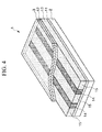
- FIG. 4 is an enlarged perspective view showing only the optical waveguide in the optical wiring part shown in FIG. 1 .
- the up side in Fig. 3 is represented by "up side” and the down side in Fig. 3 is represented by “down side” in the following descriptions.
- the optical wiring part 10 shown in FIG. 1 includes an optical waveguide 1, and a ferrule 5 which is provided at the end of the optical waveguide 1.
- the optical waveguide 1 shown in FIG. 1 has a long tape shape having a cross-sectional shape of which the thickness is smaller than the width.
- the optical waveguide 1 transmits optical signals between one end and the other end in the longitudinal direction.
- figures of the present application show only the vicinity of one end of the optical waveguide 1, and omit the other end of the optical waveguide 1.
- the vicinity of the other end of the optical waveguide 1 has the same structure as that of one end of the optical waveguide 1.
- “one end” and “one end surface” of the optical waveguide 1 shown in figures may be represented by "tip end", and "tip end surface” in the present description.
- the optical waveguide 1 is a laminate having a clad layer 11, a core layer 13, and a clad layer 12, in this lamination order from the bottom.
- the core layer 13 shown in FIG. 4 has two long core portions 14 and 14 which are arranged in parallel and side clad portions 15, 15, and 15 which are adjacent to the side surfaces of each core portion 14.
- a ferrule 5 is provided so as to cover the tip end of the optical waveguide 1.
- the ferrule 5 has a penetration hole 50.
- the tip end of the optical waveguide 1 is inserted into the penetration hole 50.
- One end surface of the ferrule 5 and the tip end surface of the optical waveguide 1 are aligned with each other.
- “one end” and “one end surface” of the ferrule 5 in figures are represented by “tip end” and "tip end surface” in the present description.
- the other end of the ferrule 5 which is an insertion opening for the optical waveguide 1 is represented by "base end”.
- the surface of the other end of the ferrule 5 is represented by "base end surface”.
- the penetration hole 50 is formed in the ferrule 5 from the base end to the tip end.
- the ferrule 5 includes a main body 51 having a groove 501 formed from the tip end to the base end of the main body 51, a lid body 52 which is housed in the groove 501 and covers the upper opening of the groove 501.
- FIG. 2 shows a state before covering the groove 501 with the lid body 51, that is, a disassembly state of the ferrule 5.
- a surface positioned at the bottom of the groove 501 is represented by a bottom surface 5011
- two surfaces which stand upwardly from the bottom surface 5011 are represented by side surfaces 5012 and 5012 in the groove 501 shown in FIG. 2 .
- the penetration hole 50 shown in FIG. 1 is formed by housing the lid body 52 in the groove 501.
- the lower surface of the penetration hole 50 is formed by the bottom surface of the groove 501
- both side surfaces of the penetration hole 50 are formed by the side surfaces of the groove 5012 and 5012
- the upper surface of the penetration hole 50 is formed by the lower surface 521 of the lid body 52.
- the optical wiring part 10 is produced by inserting the tip end of the optical waveguide 1 into the penetration hole 50, and fixing the optical wiring part 10 and the ferrule 5.
- the upper opening of the groove 501 is covered with the lid body 52 means that the lid body 52 is mounted so as to cover the upper opening and thereby the groove 501 is changed to substantial "a hole". At this time, it is not necessary that the main body 51 is in contact with the 1id body 52.
- the lower surface 101 at the tip end of the optical waveguide 1 is fixed to the bottom surface 5011 of the groove 501 by an adhesive layer 55 in the optical wiring part 10.
- the upper surface 102 at the tip end of the optical waveguide 1 is fixed to the bottom surface 521 of the lid body 52 by an adhesive layer 56.
- the both side surfaces 103 and 103 at the tip end of the optical waveguide 1 are positioned apart from an inner wall of the groove 501. There is a clearance between the both side surfaces 103 and 103 of the optical waveguide 1 and the side surfaces 5012 and 5012 of the groove 501 respectively. Therefore, in the optical wiring part 10 shown in FIG. 1 , the lid body 52 is indirectly fixed to the main body 51 via the optical waveguide 1, not directly fixed to the main body 51.
- both the two main surfaces of the tape-shaped optical waveguide 1 are fixed to the inner wall of the penetration hole 50 whilst both the side surfaces of the optical waveguide 1 are positioned apart from the inner wall of the penetration hole 50, and there is a clearance between both the side surfaces of the optical waveguide 1 and the inner wall of the penetration hole 50.
- the side surfaces of the lid body 52 are also positioned apart from the side surfaces 5012 and 5012 of the groove 501, and there is a clearance between them.
- the two main surfaces that is, the lower surface 101 and the upper surface 102 are fixed to the inner wall of the penetration hole 50 by the adhesive layers 55 and 56, each of the two side surfaces 103 and 103 is positioned apart from the inner wall of the penetration hole 50, and there is a clearance between the two side surfaces of the optical waveguide 1 and the inner wall of the penetration hole 50.
- the optical wiring part 10 having such a structure the increase of the transmission loss caused by the local stress concentration can be inhibited while the optical waveguide 1 and the ferrule 5 are reliably fixed. Thereby, it is possible to obtain high transmission efficiency of the optical waveguide 1 in the environment of large temperature change, and even in the environment of high humidity.
- the optical wiring part 1 which is in contact with another optical part with high transmission efficiency can be produced.
- the lower surface 101 and the upper surface 102 occupy most of the surface area of the tip end of the tape-shaped optical waveguide 1. Therefore, the fixing state can be stably maintained for a long period of time by fixing the lower surface 101 and the upper surface 102 of the optical waveguide 1 to the inner wall of the penetration hole 50. As a result, the optical wiring part 10 having high reliability can be obtained.
- the positioning of the lid body 52 in the groove 501 can be easily adjusted by housing the lid body 52 in the groove 501. Therefore, assembly operation is facilitated.
- the lid body 52 is indirectly fixed to the main body 51 via the optical waveguide 1, not directly fixed to the main body 51, the lid body 52 can move following the motion of the optical waveguide 1 while protecting the optical waveguide 1. In other words, the 1id body 52 can move independently from the main body 51. Therefore, the lid body 52 can protect the optical waveguide 1 without generating the stress concentration in the optical waveguide 1.
- the lower surface and both the side surfaces are formed by the groove 501 and the upper surface 502 is the lower surface 521 of the lid body 52. Therefore, when the optical waveguide 1 is inserted into the penetration hole 50, first, the optical waveguide 1 is housed in the groove 501, and then the lid 52 is mounted so as to cover the upper opening of the groove 501. That is, the optical waveguide 1 is housed in the penetration hole 50 while forming the penetration hole 50. Therefore, the assembly operation is facilitated compared with a case in which the optical waveguide 1 is inserted into the penetration hole 50.
- the clearance L1 (as shown in FIG. 3A ) between the side surface of the optical waveguide1 and the side surface 5012 of the groove 501 is suitably adjusted depending on the size of the optical waveguide 1 or the ferrule, and not particularly limited.
- the clearance L1 is preferably about 5 ⁇ m to about 1,000 ⁇ m, more preferably about 10 ⁇ m to about 750 ⁇ m, still more preferably about 15 ⁇ m to about 500 ⁇ m, and most preferably about 25 ⁇ m to about 350 ⁇ m.
- the clearance L1 is in the above-identified range, it is possible to sufficiently inhibit a decrease of the transmission efficiency even in an environment of large temperature change, and a remarkable enlargement of the optical wiring part.
- the clearance L1 between the side surface of the optical waveguide 1 and the side surface 5012 of the groove 501 may be partially outside the above-identified range.
- the area of the region having the clearance L1 outside the above-identified range is preferably 30% or less relative to the total area of the side surface 5012 of the groove 501.
- the clearance L1 it is possible to widen the range of the clearance L1 to 0.001 ⁇ m to 1,000 ⁇ m, more preferably 0.1 ⁇ m to 500 ⁇ m, and most preferably 1 ⁇ m to 200 ⁇ m by subjecting at least one of the side surface 103 of the optical waveguide 1 and the side surface 5012 of the groove 501 to a release treatment. Thereby, the possibility of the design freedom of the optical wiring part 10 as well as the stress concentration is certainly reduced.
- Examples of the release treatment include a treatment in which a releasing agent is coated to a surface to be treated, a treatment in which a releasing agent is coated and a releasing layer is formed on a surface to be treated, and a surface modification treatment, such as a plasma treatment.
- Examples of the releasing agent include a fluorine-based releasing agent, a silicone-based releasing agent, a polyethylene-based releasing agent, a polypropylene-based releasing agent, a paraffin-based releasing agent, a montane-based releasing agent, and a carnauba-based releasing agent.
- the releasing agent can be used alone or combination of two or more.
- the clearance between the lid body 52 and the side surface 5012 of the groove 501 is the same as the clearance L1 explained above.
- the clearance L2 (as shown in FIG. 3A ) between the upper surface 102 of the optical wavelength 1 and the lower surface 521 of the lid body 52, that is, the thickness of the adhesive layer 56 is also adjusted depending on the size of the optical wavelength 1 and the ferrule 5.
- the clearance L2 is preferably about 10 ⁇ m to about 2,000 ⁇ m, more preferably about 15 ⁇ m to about 1,000 ⁇ m, still more preferably about 100 ⁇ m to about 1,000 ⁇ m, and most preferably about 300 ⁇ m to about 800 ⁇ m. It is possible to reliably fix the optical wavelength 1 to the ferrule 5 by setting the clearance L2 to be in the above-identified range.
- the clearance L2 between the upper surface 102 of the optical wavelength 1 and the lower surface 521 of the lid body 52 may be locally outside the above-identified range.
- the area of the region having the clearance L2 outside the above-identified range is preferably 30% or less relative to the total area of the upper surface 102 of the optical wavelength 1 or the lower surface 521 of the lid body 52.
- the clearance L2 may be smaller, equal, or larger than the clearance L1.
- the clearance L2 is preferably about 30 to about 300%, and more preferably about 50 to about 200%, of the clearance L1. It is possible to reliably fix the optical wavelength 1 to the ferrule 5 by setting the clearances L1 and L2 to be in the above-identified range.
- the thickness of the adhesive layer 55 formed on the upper surface 102 of the optical waveguide 1 may be different from the thickness of the adhesive layer 56 formed on the lower surface 101 of the optical waveguide 1.
- the optical waveguide 1 is a long member having a tape-shape in plane view, and transmits optical signals from one end to the other end.
- Two core portions 14 and 14 shown in FIG. 4 are covered with the clad portions (side clad portions 15, 15, and 15, and clad layers 11 and 12). Thereby, it is possible to transmit light while light is confined in the core portion 14.
- the refractive index of the core portion 14 may be larger than the refractive index of the clad portion.
- the difference between the refractive index of the core portion 14 and the clad portion is preferably 0.3% or more, and more preferably 0.5% or more.
- the upper value of the difference between the refractive index of the core portion 14 and the clad portion is not particularly limited. However, the upper value is preferably about 5.5%.
- the refractive index difference is less than the lower limit of the above-identified range, the transmission efficiency of light may be decreased.
- the refractive index difference is more than the upper limit of the above-identified range, further improvement of the transmission efficiency is not desired.
- the refractive index difference can be represented by the following equation when the refractive index of the core portion 14 is represented by A, and the refractive index of the clad portion is represented by B.
- Refractive Index Difference % A / B - 1 x 100
- the refractive index distribution in the width direction at the cross section of the core portion 14 may have any shapes.
- the refractive index distribution may be a so-called step index (SI) type distribution in which the refractive index discontinuously changes or a so-called graded index (GI) type distribution in which the refractive index continuously changes.
- SI step index
- GI graded index
- the core portion 14 may be straight or curved in the plan view. Furthermore, the core portion 14 may be branched or crossed on the route.
- the cross-sectional shape of the core portion 14 is not particular limited.
- Examples of the cross-sectional shape of the core portion 14 include a circle, such as a perfect circle, an oval, and an elliptical, a polygon, such as a triangle, a square, a pentagon, and a hexagon.
- the cross-sectional shape of the core portion 14 is a square, the core portion 14 is easily produced.
- the width and the height (that is, the thickness) of the core portion 14 are not particularly limited. However, the width and height of the core portion 14 are preferably about 1 ⁇ m to about 200 ⁇ m, more preferably about 5 ⁇ m to about 100 ⁇ m, and most preferably about 10 ⁇ m to about 70 ⁇ m. When the width and height of the core portion 14 are in the above-identified range, it is possible to increase the density of the core portion 14 while suppressing a decrease of the transmission efficiency of the optical waveguide 1.
- the width of the side clad portions 15 between the core portions 14 and 14 is preferably about 5 ⁇ m to about 250 ⁇ m, more preferably about 10 ⁇ m to about 200 ⁇ m, and most preferably about 10 ⁇ m to about 120 ⁇ m.
- the width of the side clad portions 15 is in the above-identified range, it is possible to increase the density of the core portion 14 while suppressing the crosstalk of optical signals between the core portions 14 and 14.
- a constituent material (main material) of the core layer 13 examples include a resin, for example, cyclic ether-base resin, such as an acrylic-based resin, a methacrylic-based resin, polycarbonate, polystyrene, an epoxy-based resin, and an oxetane-based resin, polyamide, polyimide, polybenzoxazole, polysilane, polysilazane, a silicone-based resin, a fluorine-based resin, polyurethane, a polyolefin-based resin, polybutadiene, polyisoprene, polychloroprene, polyester, such as PET and PBT, polyethylene succinate, polysulfone, polyether, and a cyclic olefin-based resin, such as a benzocyclobutene-based resin, and a norbornene-based resin, and glass, such as quartz glass, and borosilicate glass.
- the resin material may be a composition containing two or more kinds
- the average thickness of the clad layer 11 and 12 is preferably about 0.05 times to about 1.5 times as much as the average thickness of the core layer 13, and more preferably about 0.1 times to about 1.25 times. Specifically, the average thickness of the clad layer 11 and 12 is preferably about 1 ⁇ m to about 200 ⁇ m, more preferably about 3 ⁇ m to about 100 ⁇ m, and most preferably about 5 ⁇ m to about 60 ⁇ m. When the average thickness of the clad layer 11 and 12 is in the above-identified range, it is possible to maintain the functions of the clad portions while suppressing an increase of the thickness of the optical waveguide 1 to no more than necessary.
- the constituent material of the clad layer 11 and 12 can be used as the same constituent material of the core layer 13.
- the clad layer 11 and 12 is preferably made of at least one selected from the group consisting of a (meth)acrylic-based resin, an epoxy-based resin, a silicone-based resin, a polyimide-based resin, a fluorine-based resin, and a polyolefin-based resin, and more preferably a (meth)acrylic-based resin or an epoxy-based resin.
- the refractive index distribution in the thickness direction at the cross section of the optical waveguide 1 is not particularly limited.
- the refractive index distribution may be a SI type or a GI type.
- the width of the optical waveguide 1 is not particularly limited, and is preferably about 2 mm to about 100 mm, and more preferably about 3 mm to about 50 mm.
- the number of the core portion 14 in the optical waveguide 1 is not particularly limited, and preferably about 1 to about 100.
- the optical waveguide 1 can be multilayered if necessary. Specifically, the optical waveguide 1 can be multilayered by positioning the core layer and the clad layer alternately on the optical waveguide 1 shown in FIG. 4 .
- the optical waveguide 1 shown in FIG. 4 includes a support film 2 as a bottom layer and a cover film 3 as a top layer.
- constituent material of the support film 2 and the cover film 3 examples include resin, for example, polyolefin, such as polyethylene terephthalate (PET), polyethylene, and polypropylene, polyimide, and polyamide.
- polyolefin such as polyethylene terephthalate (PET)
- PET polyethylene terephthalate
- polyethylene polyethylene
- polypropylene polypropylene
- polyimide polyimide
- polyamide polyamide
- the average thickness of the support film 2 and the cover film 3 is not particularly limited. However, the average thickness of the support film 2 and the cover film 3 is preferably about 5 ⁇ m to about 500 ⁇ m and more preferably about 10 ⁇ m to about 400 ⁇ m. When the average thickness of the support film 2 and the cover film 3 is in the above-identified range, the support film 2 and the cover film 3 have suitable stiffness. Thereby, it is possible to reliably protect the core layer from external force or external environment while reliably supporting the core layer 13.
- the clad layer 11 and the support film2, and the clad layer 12 and the cover layer 3 are adhered by an adhesive agent, a tacky agent, an adhesive sheet, a tacky sheet, or thermocompression
- the ferrule 5 is provided with a tope end of the optical waveguide 1.
- the ferrule 5 connects optically the optical waveguide 1 and another optical part.
- the ferrule 5 may contains a part confirming to various connector standard. Examples of the connector standard include small size (Mini) MT connector, and MT connector, 16 MT connector, two-dimensional array type MT connector, MPO collector, and MPX connector which are prescribed in JIS C 5981.
- two guide holes 511 and 511 are formed at the tip end surface of the main body 51 of the ferrule 5 in this embodiment.
- the guide holes 511 and 511 are formed so as to penetrate from the base end surface to the tip end surface of the ferrule 5.
- guide pins of the other optical part are inserted into the guide holes 511 and 511.
- both optical wiring part 10 and another optical part can be fixed. That is, the guide hole 511 is used as a connection mechanism configured to connect the optical waveguide 1 and another optical part.
- the guide hole 511 is not always formed in the base end surface as long as the guide hole 511 is formed in the tip end surface.
- a locking structure using a claw, or an adhesive agent can be used to connect them.
- the penetration hole 50 of the ferrule 5 may have the same cross sectional shape from the base end to tip end, or may have a different cross sectional shape in the middle.
- the height of the penetration hole 50 gradually increases toward the base end surface in the ferrule 5 in this embodiment.
- a part of the bottom surface 5011 at the base end side of the groove 501 is curved such that the inclination angle toward the lower side is gradually larger toward the base end.
- a curved surface 5011a is formed at a part of the bottom surface 5011 on the base end side, and the curvature is gradually increased toward the base end.
- a part of the bottom surface 521 of the lid body 52 on the base end side is curved such that the inclination angle toward the upper side is gradually larger toward the base end.
- a curved surface 521a is formed at a part of the bottom surface 521 on the base end side, and the curvature is gradually increased toward the base end.
- the optical waveguide 1 is curved along the bottom surface 5011 or the bottom surface 521. That is, the optical waveguide 1 is gently curved along the curved surface 5011a or the curved surface 521a. It is possible to inhibit the abrupt bending of the optical waveguide 1. As a result, it is possible to prevent the occurrence of problems, such as a decrease of the transmission efficiency or the disconnection, which are caused by the abrupt bending.
- the optical waveguide 1 to which external force is added, is in contact with the bottom surface 5011 of the groove 501 or the bottom surface 521 of the lid body 52, the optical waveguide 1 moves relatively freely in accordance with the external force. Thereby, since the external force can be easily released, it is possible to prevent the optical waveguide 1 from falling out from the penetration hole 50.
- the length L3 of the curved surface 5011a in the bottom surface 5011 and the length L3 of the curved surface 521 in the bottom surface 521 are preferably about 5% to about 50% relative to the total length L4 of the ferrule 5, and more preferably about 10% to about 40%.
- the optical wavelength 1 is reliably fixed to the ferrule 5 and high durability of the optical wiring part 10 can be obtained.
- the ratio L3/L4 is less than the lower limit of the above-identified range, the tolerance to external force of the optical wiring part 10 may be decreased.
- the ratio L3/L4 is more than the upper limit of the above-identified range, the fixing force decreases, and fixation may be released by pulling the optical waveguide 1 with great force.
- Examples of the constituent material of the ferrule 5 include resin, such as a phenol-based resin, an epoxy-based resin, an olefin-based resin, a urea-based resin, a melamine-based resin, and an unsaturated polyester-based resin, and a metal material such as stainless steel, and an aluminum alloy.
- resin such as a phenol-based resin, an epoxy-based resin, an olefin-based resin, a urea-based resin, a melamine-based resin, and an unsaturated polyester-based resin
- a metal material such as stainless steel, and an aluminum alloy.
- the main body 51 and the lid body 52 of the ferrule 5 are completely separated in this embodiment.
- the main body 51 and the lid body 52 may be partially connected with each other.
- the main body 51 and the 1id body 52 are partially connected with each other, they can be integrally handled.
- the working efficiency, such as assembly operation efficiency of the optical wiring part 10 can be improved.
- the connection part may be made of a rubber material, a resin material, or the like.
- connection part is made of the same material as that of the ferrule 5, and the connection part is made by a fine linear part to decrease the rigidity, essentially the same functions and effects as those which are obtained in a case that the main body 51 and the lid body 52 are separated can be obtained.
- the constituent material of the adhesive layer 55 and 56 are, for example, a cured adhesive agent or a cured bonding sheet.
- the adhesive agent examples include an epoxy-based adhesive agent, an acrylic-based adhesive agent, an urethane-based adhesive agent, a silicone-based adhesive agent, and an olefin-base adhesive agent, and various hot melt adhesive agents (a polyester-based hot melt adhesive agent, a modified olefin-based hot melt adhesive agent).
- the constituent material of the bonding sheet examples include a bisphenol-type epoxy resin, such as a bisphenol A epoxy resin, a bisphenol F epoxy resin, a bisphenol AD epoxy resin, and a bisphenol S epoxy resin, a novolak epoxy resin, such as a phenol novolak epoxy resin, and a cresol novolak epoxy resin, an aromatic epoxy resin such as a trisphenol methane triglycidyl ether, various epoxy resins, such as a naphtalene type epoxy resin, and a dicyclopentadiene type epoxy resin, an imide resin, such as polyimide and polyamideimide, a silicone resin, a phenol resin, and a urea resin.
- the resin may be used alone or in combination of two or more.
- the constituent material of the bonding sheet may further include rubber, such as acrylonitrile-butadiene rubber (NBR), carboxyl-terminated NBR (CTBN), styrene-butadiene rubber (SBR), polybutadiene, and acrylic rubber, and a thermoplastic resin, such as a vinyl acetate resin, a polyvinyl alcohol resin, a polyvinyl acetal resin, an acrylic resin, a polyacrylonitrile resin, a vinyl urethane resin, a polyester resin, and a polyamide resin.
- the amount of the rubber and the thermoplastic resin relative to 100 parts by mass of the themosetting resin is preferably about 10 to about 200 parts by mass, and more preferably about 20 to about 150 parts by mass.
- the elongation modulus (Young's modulus) of the adhesive layer 55 and 56 slightly varies depending on the size of the optical waveguide 1, the clearance L2, or the like, and is preferably about 100 MPa to about 20,000 MPa, more preferably about 300 MPa to about 15,000 MPa, still more preferably about 500 MPa to about 12,500 MPa, and most preferably about 1,000 MPa to about10,000 MPa.
- the elongation modulus of the adhesive layer 55 and 56 is adjusted to be in the above-identified range, the stress concentration in the optical waveguide 1 is reliably reduced, and the increase of the transmission loss is inhibited, while the optical waveguide is reliably fixed to the ferrule 5.
- the elongation modulus of the adhesive layer 55 and 56 is measured in accordance with JIS K 7127, and the measurement temperature is set to 25°C.
- the glass-transition temperature of the adhesive layer 55 and 56 is preferably about 30°C to about 180°C, and more preferably about 35°C to about 140°C.
- the heat resistance of the optical wiring part 10 can be further improved.
- the glass-transition temperature of the adhesive layer 55 and 56 is measured by a dynamic viscoelasticity determination method (DMA method).
- DMA method dynamic viscoelasticity determination method
- the side surfaces 103 and 103 of the optical waveguide 1 are positioned apart from the side surfaces 5012 and 5012 of the groove 501, and there is a clearance between the two side surfaces of the optical waveguide 1 and the inner wall of the penetration hole 50 in this embodiment.
- the adhesive layers 55 and 56 be also positioned apart from the side surfaces 5012 and 5012 of the groove 501. Thereby, it is possible to reliably suppress the local stress concentration in the optical waveguide 1.
- the clearance between the side surfaces of the adhesive layers 55 and 56 and the side surfaces 5012 and 5012 of the groove 501 is set in the same manner as the clearance L1.
- FIG. 5 is a perspective view showing the second embodiment of the optical wiring part according to the invention.
- FIG. 6A is a sectional view of the optical wiring part which is taken along line A-A of FIG. 5 .
- FIG. 6B is a sectional view of the optical wiring part which is taken along line B-B of FIG. 5 .
- the second embodiment will be explained while focusing different components from the first embodiment, and the explanation about the same components as those in the first embodiment will be omitted. Moreover, the same components in FIGS. 5 , 6A, and 6B as those in the first embodiment are represented by the same reference numbers, and the detail explanation of the components are omitted.
- the optical wiring part of this embodiment has the same components as those of the first embodiment, except that the ferrule 5 has a different structure from the ferrule 5 in the first embodiment.
- the main body 51 and the lid body 52 are not separated and integrated in the ferrule 5 shown in FIG. 5 . Therefore, the ferrule 5 shown in FIG 5 does not have a clearance between the lid body 52 and the main body 51, which the ferrule shown in FIG 1 includes.
- the ferrule 5 shown in FIG. 5 has the penetrate hole 50 from the base end to the tip end of the ferrule 5.
- the tip end of the optical waveguide 1 is inserted into the penetration hole 50.
- the bottom inner wall is represented by "bottom surface 5001”
- the upper inner wall is represented by "upper surface 5002”
- the side inner wall is represented by "side surface 5003”.
- the lower surface 101 of the tip end of the optical waveguide 1 and the bottom surface 5001 of the penetration hole 50 are adhered by the adhesive layer 55 similar to the first embodiment.
- the side surfaces 103 and 103 of the tip end of the optical waveguide 1 are positioned apart from the side surfaces 5003 and 5003 of the penetration hole 50, and there is a clearance between the two side surfaces of the optical waveguide 1 and the inner wall of the penetration hole 50.
- the upper surface 102 of the tip end of the optical waveguide 1 is positioned apart from the upper surface 5002 of the penetration hole 50, and there is a clearance between them.
- the optical wiring part 10 having such a structure has the same functions and effects as those of the optical wiring part 10 of the first embodiment.
- the clearance L2 between the upper surface 102 of the optical wavelength 1 and the upper surface 5002 of the penetration hole 50 is preferably about 30 to about 300% of the clearance L1 between the side surface 103 of the optical waveguide1 and the side surface 5003 of the penetration hole 50, and more preferably about 50 to about 200%.
- the ratio L2/L1 is in the above-identified range, it is possible to reliably fix the optical waveguide 1 in the ferrule 5 with high accuracy.
- the thickness of the adhesive layer 55 is preferably equal to the clearance L2 or less.
- the thickness of the adhesive layer 55 is equal to the clearance Ls or less, it is possible to suppress the inclination of the optical waveguide 1 depending on the variation of the thickness of the adhesive layer 55.
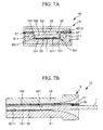
- FIG. 7A shows a third embodiment of the optical wiring part, and is a sectional view showing the optical wiring part when the ferrule is cut in an orthogonal direction relative to a longitudinal direction of the ferrule.
- FIG. 7B is a sectional view showing an optical wiring part when the ferrule is cut in a longitudinal direction of the ferrule.
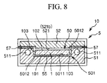
- FIG. 8 is a sectional view showing an alternative optical wiring part shown in FIG. 7 .
- the third embodiment will be explained while focusing different components from the first and second embodiments, and the explanation about the same components as those in the first and second embodiments will be omitted. Moreover, the same components in FIGS. 7A, 7B , and 8 , as those in the first embodiment are represented by the same reference numbers, and the detail explanation of the components are omitted.
- the optical wiring part of this embodiment has the same components as those of the first embodiment, except that the ferrule 5 has a different structure from the ferrule 5 in the first embodiment.
- the upper surface of the main body 51 and the lower surface 521 of the lid body 52 are adhered and fixed via an adhesive layer 57.
- the upper surface 102 of the optical waveguide 1 is positioned apart from the lower surface 521 of the lid body 52, and there is a clearance between them.
- the clearance between the upper surface 102 of the optical waveguide 1 and the lower surface 521 of the lid body 52 can be easily adjusted by suitably changing the thickness of the adhesive layer 57. Therefore, it is possible to flexibly change the clearance between the upper surface 102 of the optical waveguide 1 and the lower surface 521 of the lid body 52 depending on the thickness of the optical waveguide 1 inserted into the penetration hole 50 in the ferrule 5 shown in FIGS. 7A and 7B .
- the optical wiring part 10 has high general usefulness.
- the optical wiring part 10 having such a structure has the same functions and effects as those in the first and second embodiments.
- a part of the lower surface 521 of the lid body 52 may protrude downwardly as shown in FIG. 8 .
- the clearance between the upper surface 102 of the optical waveguide 1 and the lower surface 521 of the lid body 52 can be adjusted by changing the protrusion amount of the protrusion portion 521b. Therefore, it is possible to change the clearance between the upper surface 102 of the optical waveguide 1 and the lower surface 521 of the 1id body 52 depending on the thickness of the optical waveguide 1 inserted into the penetration hole 50 in the ferrule 5 shown in FIGS. 8 .
- the optical wiring part 10 has high general usefulness.
- the protrusion portion 521b is housed in the groove 501, the positioning between the main body 51 and the lid body 52 is facilitated.
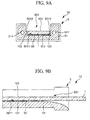
- FIG. 9A shows the fourth embodiment of the optical wiring part according to the present invention, and is a sectional view showing an optical wiring part when the ferrule is cut in an orthogonal direction relative to a longitudinal direction of the ferrule.
- FIG. 9B is a longitudinal sectional showing the optical wiring part.
- the fourth embodiment will be explained while focusing different components from the first to third embodiments, and the explanation about the same components as those in the first embodiment will be omitted. Moreover, the same components in FIGS. 9A and 9B as those in the first embodiment are represented by the same reference components, and the detail explanation of the components are omitted.
- the optical wiring part of this embodiment has the same components as those of the first embodiment, except that the ferrule 5 has a different structure from the ferrule 5 in the first embodiment.
- the ferrule 5 shown in FIGS. 9A and 9B has a structure in which the lid body 52 is omitted from the ferrule 5 shown in FIG. 3 .
- Both the side surfaces 103 and 103 at the tip end of the optical waveguide 1 are positioned apart from the inner wall of the groove 501, and there is a clearance between them in the ferrule 5.
- the lower surface 101 at the tip end of the optical waveguide 1 is fixed to the bottom surface 5011 of the groove 501 via an adhesive layer 55.
- the upper surface 102 of the optical waveguide 1 at the tip end faces the upper opening of the groove 501.
- the optical wiring part of this embodiment has the same functions and effects as those of the first to third embodiments.
- the groove 501 may be filled with a filler if necessary.
- the filler is not enter in the clearance between both the side surface 103 and 103 at the tip end of the optical waveguide 1 and the side walls 5012 and 5012 of the groove 501.
- a curable filler it is possible to prevent the curable filler from entering the clearance by optimizing the fluidity of the filler before curing.
- a spacer may be inserted into the clearance, the filler may be filled in the groove while inserting the spacer, and the spacer may be removed after curing.
- the decrease of the transmission efficiency is suppressed in the optical wiring part when the optical waveguide is connected with another optical part. Therefore, it is possible to obtain an electronic device (electronic device of the present invention) which can optically communicate with high quality, and has high reliability by using the optical wiring part according to the present invention.
- Examples of the electronic device having the optical wiring part according to the present invention include a mobile phone, a game machine, a router device, a WDM device, a personal computer, a television, and a home server.
- a mobile phone a game machine
- a router device a WDM device
- a personal computer a personal computer
- a television and a home server.
- a home server it is necessary to transmit large data between an arithmetic unit, such as LSI, and a memory unit, such as RAM. Therefore, when the electronic device has the optical wiring part according to the present invention, it is possible to remove defects, such as noise specific to electric wirings, and signal degradation, and remarkable improvement of the performance can be expected.
- the calorific value can be drastically reduced in the optical waveguide compared with electric wirings. Therefore, electric power for cooling is largely reduced. The electricity consumption of entire electronic device can also be reduced.
- optical wiring part and the electronic device having the optical wiring part according to the present invention are explained based on the embodiments together with figures.
- the present invention is not limited to the embodiments and figures.
- the ferrule is provided with one end of the optical waveguide in the embodiments.
- a different ferrule, or a connector may be provided with the other end of the optical waveguide.
- a light emitting and receiving element may be mounted at an optical path conversion portion.
- the ferrule or the like may not be mounted at the other end of the optical waveguide.
- An epoxy-based adhesive agent (Young's modulus: 2,000 MPa) was coated to the upper and lower surfaces at the tip end of an optical waveguide made of a norbornene resin.
- the optical waveguide has 80 mm in length and 48 core portions.
- a ferrule having a shape shown in FIG. 2 which was made of polyphenylene sulfide (PPS) was prepared. Then, the tip end of the optical waveguide was housed in a groove formed in a main body of the ferrule. At this time, the tip end surface of the optical waveguide and the tip end surface of the ferrule were aligned with each other.
- PPS polyphenylene sulfide
- the clearance L1 was 200 ⁇ m.
- the optical waveguide was obtained in a manner identical to that of Example 1, except that the clearance the clearance L1 between the side surfaces of the optical waveguide and the side surfaces of the lid body, and the clearance L1 between the side surfaces of the optical waveguide and the side surfaces of the groove were changed to 350 ⁇ m.
- the optical waveguide was obtained in a manner identical to that of Example 1, except that the clearance the clearance L1 between the side surfaces of the optical waveguide and the side surfaces of the lid body, and the clearance L1 between the side surfaces of the optical waveguide and the side surfaces of the groove were changed to 500 ⁇ m.
- the optical waveguide was obtained in a manner identical to that of Example 1, except that the clearance L1 between the side surfaces of the optical waveguide and the side surfaces of the lid body, and the clearance L1 between the side surfaces of the optical waveguide and the side surfaces of the groove were changed to 100 ⁇ m respectively.
- the optical waveguide was obtained in a manner identical to that of Example 1, except that the clearance the clearance L1 between the side surfaces of the optical waveguide and the side surfaces of the lid body, and the clearance L1 between the side surfaces of the optical waveguide and the side surfaces of the groove were changed to 200 ⁇ m.
- An epoxy-based adhesive agent (Young's modulus: 2,000 MPa) was coated to the lower surface at the tip end of the same optical waveguide as that of Example 1.
- a ferrule having a shape shown in FIGS. 6A and 6B was prepared, and the tip end of the optical waveguide was inserted into a penetration hole formed in the main body of the ferrule. At this time, the tip end surface of the optical waveguide and the tip end surface of the ferrule were aligned with each other.
- the clearance L1 was 200 ⁇ m.
- the clearance was 5 ⁇ m.
- the clearance was 200 ⁇ m.
- the optical waveguide was obtained in a manner identical to that of Example 6, except that the clearance L1 between the side surfaces of the optical waveguide and the side surfaces of the penetration hole was changed to 300 ⁇ m, and the clearance between the upper surface of the optical waveguide and the upper surface of the penetration hole was changed to 450 ⁇ m.
- An epoxy-based adhesive agent (Young's modulus: 2,000 MPa) was coated to the lower surface at the tip end of the same optical waveguide as that of Example 1.
- a ferrule having a shape shown in FIGS. 7A and 7B which was made of polyphenylene sulfide (PPS) was prepared. Then, the tip end of the optical waveguide was housed in a groove formed in a main body of the ferrule. At this time, the tip end surface of the optical waveguide and the tip end surface of the ferrule were aligned with each other.
- PPS polyphenylene sulfide
- the adhesive agent used to adhere between the lid body and the main body was also the above-identified epoxy-based agent. After that, the adhesive agent was cured. Thereby, the assembly operation was completed, and an optical wiring part shown in FIGS. 7A and 7B was obtained.
- the clearance was 250 ⁇ m.
- the clearance was 5 ⁇ m.
- the clearance was 500 ⁇ m.
- the optical waveguide was obtained in a manner identical to that of Example 8, except that the clearance between the side surfaces of the optical waveguide and the side surfaces of the penetration hole was changed to 150 ⁇ m, and the clearance between the upper surface of the optical waveguide and the upper surface of the penetration hole was changed to 250 ⁇ m.
- An epoxy-based adhesive agent (Young's modulus: 2,000 MPa) was coated to the lower surface at the tip end of the same optical waveguide as that of Example 1.
- a ferrule having a shape shown in FIGS. 9A and 9B which was made of polyphenylene sulfide (PPS) was prepared. Then, the tip end of the optical waveguide was housed in a groove formed in the ferrule. At this time, the tip end surface of the optical waveguide and the tip end surface of the ferrule were aligned with each other.
- PPS polyphenylene sulfide
- the clearance was 200 ⁇ m.
- the clearance was 5 ⁇ m.
- the optical waveguide was obtained in a manner identical to that of Example 10, except that the clearance between the side surfaces of the optical waveguide and the side surfaces of the groove was changed to 350 ⁇ m.
- a fluorine-based coating agent (Novec 1720, marketed by Sumitomo 3M) was coated to the upper and side surfaces at the tip end of the same optical waveguide as that of Example 1.
- An optical wiring part was produced in a manner identical to that of Example 6 using the optical wavelength coated with the coating agent.
- the clearance was 5 ⁇ m.
- the clearance was 1 nm.
- a fluorine-based coating agent (Novec 1720, marketed by Sumitomo 3M) was coated to the upper and side surfaces at the tip end of the same optical waveguide as that of Example 1.
- An optical wiring part was produced in a manner identical to that of Example 6 using the optical wavelength coated with the coating agent.
- the clearance L1 was 100 nm.
- the clearance was 5 ⁇ m.
- the clearance was 10 nm.
- the optical waveguide was obtained in a manner identical to that of Example 1, except that an acrylic-based adhesive agent (Young's modulus: 3,000 MPa) was used instead of the epoxy-based adhesive agent.
- the optical waveguide was obtained in a manner identical to that of Example 1, except that the ferrule having a shape shown in FIG. 2 was used, the epoxy-based adhesive agent (Young's modulus: 2,000 MPa) was filled in a clearance between the side surfaces of the lid body and the side surfaces of the groove to adhere the optical waveguide and ferrule.
- the epoxy-based adhesive agent Youngng's modulus: 2,000 MPa
- the optical waveguide was obtained in a manner identical to that of Example 1, except that the ferrule having a shape shown in FIG. 2 was used, and the epoxy-based adhesive agent (Young's modulus: 2,000 MPa) was filled in a clearance between the optical waveguide and the groove, a clearance between the optical waveguide and the lid body, and a clearance between the lid body and the main body to adhere the optical waveguide and the ferrule.
- the epoxy-based adhesive agent Young's modulus: 2,000 MPa
- the optical waveguide was obtained in a manner identical to that of Example 6, except that the ferrule having a shape shown in FIG. 6 was used, the epoxy-based adhesive agent (Young's modulus: 2,000 MPa) was filled in a clearance between the optical wavelength and the penetration hole to adhere the optical waveguide and the ferrule.
- the optical waveguide was obtained in a manner identical to that of Example 8, except that the ferrule having a shape shown in FIG. 7 was used, the epoxy-based adhesive agent (Young's modulus: 2,000 MPa) was filled in a clearance between the optical wavelength and the groove and a clearance between the optical wavelength and the lid body to adhere the optical waveguide and the ferrule.
- the epoxy-based adhesive agent Youngng's modulus: 2,000 MPa
- the optical waveguide was obtained in a manner identical to that of Example 10, except that the ferrule having a shape shown in FIG. 9 was used, the epoxy-based adhesive agent (Young's modulus: 2,000 MPa) was filled in a clearance between the optical wavelength and the groove to adhere the optical waveguide and the ferrule.
- optical wiring part prepared in Examples and Comparative Examples was subjected to a temperature cycle test of 100 cycles, 500 cycles, and 1,000 cycles in a range of -40°C to 85°C.
- 1 cycle has the following first step to fourth step.
- Table 1 also shows the results of the temperature cycle test of the optical wavelength alone as a reference.
- optical wiring part prepared in Examples and Comparative Examples was left to stand under conditions in which the temperature was 85°C, and the humidity was 85%RH for 500 hours, 1,000 hours, and 2,000 hours.
- Table 1 also shows the results of the high temperature and high humidity test of the optical wavelength alone as a reference.
- Table 1 Shape of Ferrule Temperature cycle test (Number of cycle) High temperature and high humidity test (hours) 100 500 1000 500 1000 2000 Example1 FIG.3 Good Good Good Good Good Good Good Good Example2 FIG.3 Good Good Good Good Good Good Good Example3 FIG.3 Good Good Good Good Good Good Example4 FIG.3 Good Good Good Good Good Good Example5 FIG.3 Good Good Good Good Good Good Good Example6 FIG.6 Good Good Good Good Good Good Good Good Example7 FIG.6 Good Good Good Good Good Good Good Example8 FIG.7 Good Good Good Good Good Good Good Good Good Good Example9 FIG.7 Good Good Good Good Good Good Good Good Good Example10 FIG.9 Good Good Good Good Good Good Good Good Good Good Good Good Good Example11 FIG.9 Good Good Good Good Good Good Good Good Good Good Good Good Example12 FIG.6 Good Good Good Good Good Good Good Good Good Good Good Good Good Good Good Good Good Example 13 FIG.6 Good Good Good Good Good Good Good Good Good Good Good Good Good Good Good Example 14 FIG.
- the optical wiring part of Comparative Examples had large insertion loss and many peelings after the temperature cycle test, and remarkable increase of the insertion loss after the high temperature and high humidity test.
- an optical wiring part was produced in a manner identical to that of Examples and Comparative Examples using a bonding sheet instead of the epoxy-based adhesive agent.
- the results showing the same tends as those of using the epoxy-based adhesive agent were obtained.
- the optical wiring part according to the present invention can connect the optical waveguide and another optical element with high optical coupling efficiency while inhibiting the decrease of the transmission loss.
- the electronic device according to the present invention has high reliability.
Landscapes
- Physics & Mathematics (AREA)
- General Physics & Mathematics (AREA)
- Optics & Photonics (AREA)
- Optical Integrated Circuits (AREA)
- Mechanical Coupling Of Light Guides (AREA)
- Optical Couplings Of Light Guides (AREA)
Abstract
Description
- The present invention relates to an optical wiring part and an electronic device.
- Priority is claimed on Japanese Patent Application No.
2012-263479, filed November 30, 2012 - An optical communication technique for transferring data using optical carrier waves has been developed. In recent years, an optical waveguide or an optical fiber has been spreading as a means for transferring the optical carrier waves from one point to the other point. The optical waveguide includes a linear core portion and a clad portion disposed around the core portion. The core portion is made of a material which is substantially transparent to the light of the optical carrier wave. The clad portion is made of a material having a refractive index lower than that of the material of the clad portion.
- In the optical waveguide, light, which is introduced into the core portion from one end of the core portion, is reflected at the boundary between the core portion and the clad portion, and transferred to the other end of the core portion. A light emitting element, such as a semiconductor laser, is disposed at a light input side of the optical waveguide. A light receiving element, such as a photodiode, is disposed at a light output side. Light from the light emitting element is transferred through the optical waveguide, and received by the light receiving element. The optical communication is carried out based on a flickering pattern or an intensity variation pattern of the received light.
- Currently, the optical waveguide is generally used for short-distance light communication, whereas an optical fiber is used for long-distance light communication. Therefore, it is possible to connect a local network and a backbone network by connecting between the optical waveguide and the optical fiber.
- When the optical waveguide and the optical fiber are connected, an end surface of the optical waveguide and an end surface of the optical fiber, for example, are abutted and the abutting state is maintained (For example, Patent Document 1). A connection mechanism, in which the waveguide and the optical fiber can be engaged with each other, is used to maintain the abutting state. Specifically, a first ferrule which holds the end surface of the optical waveguide and a second ferrule which holds the end surface of the optical fiber are connected by fitting an alignment pin into a fitting hole.
- The optical waveguide disclosed in
Patent Document 1 has a tape shape, and the lower surface of the tape-shaped optical waveguide is adhered to a substrate. The first ferrule has an optical wiring-housing groove. The first ferrule is fixed to the substrate in a state that the optical waveguide is housed in the optical wiring-housing groove. Thereby, the upper surface and the side surfaces at end portion of the optical waveguide are covered with the first ferrule, and the lower surface at an end portion of the optical waveguide is covered with the substrate. Furthermore, the first ferrule is fixed by filing a space between the optical waveguide and the optical wiring-housing groove with an adhesive agent. - As explained above, the lower surface of the optical waveguide is fixed to the substrate, and the upper surface and the side surfaces of the optical waveguide are fixed to the first ferrule using an adhesive agent in Patent Document No. 1. When the first ferrule is subjected to an acceleration test, such as, for example, a heat cycle test, or put in a high temperature and high humidity environment, the transmission efficiency of the optical waveguide may be decreased near the first ferrule, and the optical coupling efficiency between the optical waveguide and the optical fiber may be decreased. In general, it is known that the transmission loss becomes large by the addition of pressure.
- [Patent Document 1] Japanese Unexamined Patent Application, First Publication No.
2011-75688 - The present inventors conducted diligent research to find the mechanism for increasing the transmission loss, and measures to limit the increase of the transmission loss. Then, the present inventors found that during the acceleration test or under a high temperature and high humidity environment, stress is concentrated by the difference in a linear expansion coefficient between the optical waveguide and the ferrule, and the stress concentration increases the transmission loss. Then, the present inventors found that the increase of the transmission loss can be inhibited by making an adequate clearance between the optical waveguide and the ferrule, maintaining the stable connection state between them, and reducing the stress concentration in the optical wavelength. Thereby, the present invention can be achieved.
- The object of the present invention is to provide an optical wiring part which can connect the optical waveguide and another optical element with high optical coupling efficiency while inhibiting the decrease of the transmission loss, and an electronic device with high reliability including the optical wiring part.
- This object can be achieved by the following present inventions (1) to (7).
- (1) An optical wiring part including a tape-shaped optical waveguide and a ferrule having a penetration hole which is formed from a base end to a tip end of the ferrule, and a part of the optical waveguide in a longitudinal direction is inserted into the penetration hole,
wherein at least one main surface of two main surfaces of the optical waveguide is fixed to an inner wall of the penetration hole, and there is a clearance between the inner wall of the penetration hole and two side surfaces of the optical waveguide. - (2) The optical wiring part according to (1), wherein the ferrule includes a main body having a groove which is a part of the penetration hole, and a lid body which forms the penetration hole together with the groove by covering an opening of the groove, and
one main surface of two main surfaces of the optical waveguide is fixed to an inner wall of the groove, and the other main surface of the optical waveguide is fixed to the lid body. - (3) The optical wiring part according to (2), wherein the lid body covers the opening of the groove in a state that at least a part of the lid body is housed in the groove.
- (4) The optical wiring part according to (3), wherein the lid body is positioned apart from the inner wall of the groove.
- (5) The optical wiring part according to (1), wherein the ferrule includes a main body having a groove which is a part of the penetration hole, and a lid body which forms the penetration hole together with the groove by covering an opening of the groove, and
the lid body is fixed to the main body except that the groove. - (6) An optical wiring part including a tape-shaped optical waveguide and a ferrule having a groove which is formed from a base end to a tip end of the ferrule, and a part of the optical waveguide in a longitudinal direction is inserted into the groove,
wherein at least one main surface of two main surfaces of the optical waveguide is fixed to an inner wall of the groove, and there is a clearance between the inner wall of the groove and two side surfaces of the optical waveguide. - An electronic device including the optical wiring part according to any one of (1) to (6).
- According to the present invention, an optical wiring part, which can connect the optical waveguide and another optical element with high optical coupling efficiency while inhibiting the decrease of the transmission loss, can be provided.
- In addition, according to the present invention, an electronic device with high reliability including the optical wiring part can also be provided.
-
-
FIG. 1 is a perspective view showing an optical wiring part of the first embodiment according to the invention. -
FIG. 2 is a perspective view showing a ferrule in the optical wiring part shown inFIG. 1 . -
FIG. 3A is a sectional view showing the optical wiring part of the first embodiment which is taken along line A-A ofFIG. 1 . -
FIG. 3B is a sectional view showing the optical wiring part of the first embodiment which is taken along line B-B ofFIG. 1 . -
FIG. 4 is an enlarged perspective view showing only the optical waveguide in the optical wiring part shown inFIG. 1 . -
FIG. 5 is a perspective view showing an optical wiring part of the second embodiment according to the invention. -
FIG. 6A is a sectional view showing the optical wiring part of the second embodiment which is taken along line A-A ofFIG. 5 . -
FIG. 6B is a sectional view showing the optical wiring part of the second embodiment which is taken along line B-B ofFIG. 5 . -
FIG. 7A is a sectional view showing an optical wiring part of the third embodiment according to the invention when the ferrule is cut in an orthogonal direction relative to a longitudinal direction of the ferrule. -
FIG. 7B is a sectional view showing an optical wiring part of the third embodiment according to the invention when the ferrule is cut in a longitudinal direction of the ferrule. -
FIG. 8 is a sectional view showing an alternative optical wiring part shown inFIG. 7 when the ferrule is cut in an orthogonal direction relative to a longitudinal direction of the ferrule. -
FIG. 9A is a sectional view showing an optical wiring part of the fourth embodiment according to the invention when the ferrule is cut in an orthogonal direction relative to a longitudinal direction of the ferrule. -
FIG. 9B is a sectional view showing an optical wiring part of the fourth embodiment according to the invention when the ferrule is cut in a longitudinal direction of the ferrule. - Below, the optical wiring part and electronic device according to the present invention will be explained in detail with reference to the preferred embodiments.
- First, the first embodiment of the optical wiring part will be explained.
-
FIG. 1 is a perspective view showing an optical wiring part of the first embodiment according to the invention.FIG. 2 is a perspective view showing a ferrule in the optical wiring part shown inFIG. 1 .FIG. 3A and 3B are a sectional view of the optical wiring part which is taken along line A-A and line B-B ofFIG. 1 .FIG. 4 is an enlarged perspective view showing only the optical waveguide in the optical wiring part shown inFIG. 1 . Moreover, the up side inFig. 3 is represented by "up side" and the down side inFig. 3 is represented by "down side" in the following descriptions. - The
optical wiring part 10 shown inFIG. 1 includes anoptical waveguide 1, and aferrule 5 which is provided at the end of theoptical waveguide 1. - The
optical waveguide 1 shown inFIG. 1 has a long tape shape having a cross-sectional shape of which the thickness is smaller than the width. Theoptical waveguide 1 transmits optical signals between one end and the other end in the longitudinal direction. Moreover, figures of the present application show only the vicinity of one end of theoptical waveguide 1, and omit the other end of theoptical waveguide 1. However, the vicinity of the other end of theoptical waveguide 1 has the same structure as that of one end of theoptical waveguide 1. In addition, "one end" and "one end surface" of theoptical waveguide 1 shown in figures may be represented by "tip end", and "tip end surface" in the present description. - As shown in
FIG. 4 , theoptical waveguide 1 is a laminate having a cladlayer 11, acore layer 13, and a clad layer 12, in this lamination order from the bottom. Thecore layer 13 shown inFIG. 4 has twolong core portions portions core portion 14. - At the tip end of the
optical waveguide 1 shown inFIG. 1 , aferrule 5 is provided so as to cover the tip end of theoptical waveguide 1. In other words, theferrule 5 has apenetration hole 50. The tip end of theoptical waveguide 1 is inserted into thepenetration hole 50. One end surface of theferrule 5 and the tip end surface of theoptical waveguide 1 are aligned with each other. Moreover, "one end" and "one end surface" of theferrule 5 in figures are represented by "tip end" and "tip end surface" in the present description. The other end of theferrule 5 which is an insertion opening for theoptical waveguide 1 is represented by "base end". The surface of the other end of theferrule 5 is represented by "base end surface". Thepenetration hole 50 is formed in theferrule 5 from the base end to the tip end. - As shown in
FIG. 2 , theferrule 5 includes amain body 51 having agroove 501 formed from the tip end to the base end of themain body 51, alid body 52 which is housed in thegroove 501 and covers the upper opening of thegroove 501. Moreover,FIG. 2 shows a state before covering thegroove 501 with thelid body 51, that is, a disassembly state of theferrule 5. Furthermore, a surface positioned at the bottom of thegroove 501 is represented by abottom surface 5011, two surfaces which stand upwardly from thebottom surface 5011 are represented byside surfaces groove 501 shown inFIG. 2 . Thepenetration hole 50 shown inFIG. 1 is formed by housing thelid body 52 in thegroove 501. That is, the lower surface of thepenetration hole 50 is formed by the bottom surface of thegroove 501, both side surfaces of thepenetration hole 50 are formed by the side surfaces of thegroove penetration hole 50 is formed by thelower surface 521 of thelid body 52. Theoptical wiring part 10 is produced by inserting the tip end of theoptical waveguide 1 into thepenetration hole 50, and fixing theoptical wiring part 10 and theferrule 5. Moreover, "the upper opening of thegroove 501 is covered with thelid body 52" means that thelid body 52 is mounted so as to cover the upper opening and thereby thegroove 501 is changed to substantial "a hole". At this time, it is not necessary that themain body 51 is in contact with the1id body 52. - As shown in
FIGS. 3A and 3B , thelower surface 101 at the tip end of theoptical waveguide 1 is fixed to thebottom surface 5011 of thegroove 501 by anadhesive layer 55 in theoptical wiring part 10. In addition, theupper surface 102 at the tip end of theoptical waveguide 1 is fixed to thebottom surface 521 of thelid body 52 by anadhesive layer 56. On the other hand, as shown inFIG. 3A , the both side surfaces 103 and 103 at the tip end of theoptical waveguide 1 are positioned apart from an inner wall of thegroove 501. There is a clearance between the both side surfaces 103 and 103 of theoptical waveguide 1 and the side surfaces 5012 and 5012 of thegroove 501 respectively. Therefore, in theoptical wiring part 10 shown inFIG. 1 , thelid body 52 is indirectly fixed to themain body 51 via theoptical waveguide 1, not directly fixed to themain body 51. - As explained above, in the
optical wiring part 10 shown inFIG. 1 , both the two main surfaces of the tape-shapedoptical waveguide 1 are fixed to the inner wall of thepenetration hole 50 whilst both the side surfaces of theoptical waveguide 1 are positioned apart from the inner wall of thepenetration hole 50, and there is a clearance between both the side surfaces of theoptical waveguide 1 and the inner wall of thepenetration hole 50. In addition, the side surfaces of thelid body 52 are also positioned apart from the side surfaces 5012 and 5012 of thegroove 501, and there is a clearance between them. - In other words, at the tip end of the tape-shaped
optical waveguide 1 of theoptical wiring part 10, the two main surfaces, that is, thelower surface 101 and theupper surface 102 are fixed to the inner wall of thepenetration hole 50 by theadhesive layers side surfaces penetration hole 50, and there is a clearance between the two side surfaces of theoptical waveguide 1 and the inner wall of thepenetration hole 50. According to theoptical wiring part 10 having such a structure, the increase of the transmission loss caused by the local stress concentration can be inhibited while theoptical waveguide 1 and theferrule 5 are reliably fixed. Thereby, it is possible to obtain high transmission efficiency of theoptical waveguide 1 in the environment of large temperature change, and even in the environment of high humidity. Theoptical wiring part 1 which is in contact with another optical part with high transmission efficiency can be produced. - In addition, the
lower surface 101 and theupper surface 102 occupy most of the surface area of the tip end of the tape-shapedoptical waveguide 1. Therefore, the fixing state can be stably maintained for a long period of time by fixing thelower surface 101 and theupper surface 102 of theoptical waveguide 1 to the inner wall of thepenetration hole 50. As a result, theoptical wiring part 10 having high reliability can be obtained. - In addition, the positioning of the
lid body 52 in thegroove 501 can be easily adjusted by housing thelid body 52 in thegroove 501. Therefore, assembly operation is facilitated. - Furthermore, since the
lid body 52 is indirectly fixed to themain body 51 via theoptical waveguide 1, not directly fixed to themain body 51, thelid body 52 can move following the motion of theoptical waveguide 1 while protecting theoptical waveguide 1. In other words, the1id body 52 can move independently from themain body 51. Therefore, thelid body 52 can protect theoptical waveguide 1 without generating the stress concentration in theoptical waveguide 1. - In addition, in the
penetration hole 50 in this embodiment, the lower surface and both the side surfaces are formed by thegroove 501 and the upper surface 502 is thelower surface 521 of thelid body 52. Therefore, when theoptical waveguide 1 is inserted into thepenetration hole 50, first, theoptical waveguide 1 is housed in thegroove 501, and then thelid 52 is mounted so as to cover the upper opening of thegroove 501. That is, theoptical waveguide 1 is housed in thepenetration hole 50 while forming thepenetration hole 50. Therefore, the assembly operation is facilitated compared with a case in which theoptical waveguide 1 is inserted into thepenetration hole 50. - The clearance L1 (as shown in
FIG. 3A ) between the side surface of the optical waveguide1 and theside surface 5012 of thegroove 501 is suitably adjusted depending on the size of theoptical waveguide 1 or the ferrule, and not particularly limited. However, the clearance L1 is preferably about 5 µm to about 1,000 µm, more preferably about 10 µm to about 750 µm, still more preferably about 15 µm to about 500 µm, and most preferably about 25 µm to about 350 µm. When the clearance L1 is in the above-identified range, it is possible to sufficiently inhibit a decrease of the transmission efficiency even in an environment of large temperature change, and a remarkable enlargement of the optical wiring part. - Moreover, the clearance L1 between the side surface of the
optical waveguide 1 and theside surface 5012 of thegroove 501 may be partially outside the above-identified range. In this case, the area of the region having the clearance L1 outside the above-identified range is preferably 30% or less relative to the total area of theside surface 5012 of thegroove 501. - It is possible to improve the smoothness (slidability) between the
optical waveguide 1 and thegroove 501 by subjecting at least one of theside surface 103 of theoptical waveguide 1 and theside surface 5012 of thegroove 501 to a release treatment. Thereby, it is possible to obtain the effects explained above even when the clearance L1 is smaller than the above-identified range. - Specifically, it is possible to widen the range of the clearance L1 to 0.001 µm to 1,000 µm, more preferably 0.1 µm to 500 µm, and most preferably 1 µm to 200 µm by subjecting at least one of the
side surface 103 of theoptical waveguide 1 and theside surface 5012 of thegroove 501 to a release treatment. Thereby, the possibility of the design freedom of theoptical wiring part 10 as well as the stress concentration is certainly reduced. - Examples of the release treatment include a treatment in which a releasing agent is coated to a surface to be treated, a treatment in which a releasing agent is coated and a releasing layer is formed on a surface to be treated, and a surface modification treatment, such as a plasma treatment. Examples of the releasing agent include a fluorine-based releasing agent, a silicone-based releasing agent, a polyethylene-based releasing agent, a polypropylene-based releasing agent, a paraffin-based releasing agent, a montane-based releasing agent, and a carnauba-based releasing agent. The releasing agent can be used alone or combination of two or more.
- Moreover, the clearance between the
lid body 52 and theside surface 5012 of thegroove 501 is the same as the clearance L1 explained above. - The clearance L2 (as shown in
FIG. 3A ) between theupper surface 102 of theoptical wavelength 1 and thelower surface 521 of thelid body 52, that is, the thickness of theadhesive layer 56 is also adjusted depending on the size of theoptical wavelength 1 and theferrule 5. However, the clearance L2 is preferably about 10 µm to about 2,000 µm, more preferably about 15 µm to about 1,000 µm, still more preferably about 100 µm to about 1,000 µm, and most preferably about 300 µm to about 800 µm. It is possible to reliably fix theoptical wavelength 1 to theferrule 5 by setting the clearance L2 to be in the above-identified range. - Moreover, the clearance L2 between the
upper surface 102 of theoptical wavelength 1 and thelower surface 521 of thelid body 52 may be locally outside the above-identified range. In this case, the area of the region having the clearance L2 outside the above-identified range is preferably 30% or less relative to the total area of theupper surface 102 of theoptical wavelength 1 or thelower surface 521 of thelid body 52. - In addition, the clearance L2 may be smaller, equal, or larger than the clearance L1. However, the clearance L2 is preferably about 30 to about 300%, and more preferably about 50 to about 200%, of the clearance L1. It is possible to reliably fix the
optical wavelength 1 to theferrule 5 by setting the clearances L1 and L2 to be in the above-identified range. - In addition, the thickness of the
adhesive layer 55 formed on theupper surface 102 of theoptical waveguide 1 may be different from the thickness of theadhesive layer 56 formed on thelower surface 101 of theoptical waveguide 1. However, it is preferable that the thickness of theadhesive layer 55 equal to the thickness of theadhesive layer 56. In this case, it is possible to equalize the stiffness of theadhesive layer 55 and theadhesive layer 56, and reduce the stress concentration or the like caused by the difference of the stiffness. - Below, each component of the
optical wiring part 10 will be explained in more detail. - The
optical waveguide 1 is a long member having a tape-shape in plane view, and transmits optical signals from one end to the other end. - Two
core portions FIG. 4 are covered with the clad portions (side cladportions clad layers 11 and 12). Thereby, it is possible to transmit light while light is confined in thecore portion 14. - The refractive index of the
core portion 14 may be larger than the refractive index of the clad portion. The difference between the refractive index of thecore portion 14 and the clad portion is preferably 0.3% or more, and more preferably 0.5% or more. The upper value of the difference between the refractive index of thecore portion 14 and the clad portion is not particularly limited. However, the upper value is preferably about 5.5%. When the refractive index difference is less than the lower limit of the above-identified range, the transmission efficiency of light may be decreased. On the other hand, when the refractive index difference is more than the upper limit of the above-identified range, further improvement of the transmission efficiency is not desired. - The refractive index difference can be represented by the following equation when the refractive index of the
core portion 14 is represented by A, and the refractive index of the clad portion is represented by B.
- The refractive index distribution in the width direction at the cross section of the
core portion 14 may have any shapes. The refractive index distribution may be a so-called step index (SI) type distribution in which the refractive index discontinuously changes or a so-called graded index (GI) type distribution in which the refractive index continuously changes. When the SI type distribution is used, the refractive index distribution can be easily formed. When the GI type distribution is used, the possibility that optical signals are collected in the region having high refractive index increases, and the transmission efficiency is improved. - In addition, the
core portion 14 may be straight or curved in the plan view. Furthermore, thecore portion 14 may be branched or crossed on the route. - Moreover, the cross-sectional shape of the
core portion 14 is not particular limited. Examples of the cross-sectional shape of thecore portion 14 include a circle, such as a perfect circle, an oval, and an elliptical, a polygon, such as a triangle, a square, a pentagon, and a hexagon. However, when the cross-sectional shape of thecore portion 14 is a square, thecore portion 14 is easily produced. - The width and the height (that is, the thickness) of the
core portion 14 are not particularly limited. However, the width and height of thecore portion 14 are preferably about 1 µm to about 200 µm, more preferably about 5 µm to about 100 µm, and most preferably about 10 µm to about 70 µm. When the width and height of thecore portion 14 are in the above-identified range, it is possible to increase the density of thecore portion 14 while suppressing a decrease of the transmission efficiency of theoptical waveguide 1. - When a plurality of
core portions 14 are positioned in a line as shown inFIG. 4 , the width of the side cladportions 15 between thecore portions portions 15 is in the above-identified range, it is possible to increase the density of thecore portion 14 while suppressing the crosstalk of optical signals between thecore portions - Examples of a constituent material (main material) of the
core layer 13 include a resin, for example, cyclic ether-base resin, such as an acrylic-based resin, a methacrylic-based resin, polycarbonate, polystyrene, an epoxy-based resin, and an oxetane-based resin, polyamide, polyimide, polybenzoxazole, polysilane, polysilazane, a silicone-based resin, a fluorine-based resin, polyurethane, a polyolefin-based resin, polybutadiene, polyisoprene, polychloroprene, polyester, such as PET and PBT, polyethylene succinate, polysulfone, polyether, and a cyclic olefin-based resin, such as a benzocyclobutene-based resin, and a norbornene-based resin, and glass, such as quartz glass, and borosilicate glass. The resin material may be a composition containing two or more kinds of resins. - The average thickness of the clad
layer 11 and 12 is preferably about 0.05 times to about 1.5 times as much as the average thickness of thecore layer 13, and more preferably about 0.1 times to about 1.25 times. Specifically, the average thickness of the cladlayer 11 and 12 is preferably about 1 µm to about 200 µm, more preferably about 3 µm to about 100 µm, and most preferably about 5 µm to about 60 µm. When the average thickness of the cladlayer 11 and 12 is in the above-identified range, it is possible to maintain the functions of the clad portions while suppressing an increase of the thickness of theoptical waveguide 1 to no more than necessary. - For example, as the constituent material of the clad
layer 11 and 12 can be used as the same constituent material of thecore layer 13. In particular, the cladlayer 11 and 12 is preferably made of at least one selected from the group consisting of a (meth)acrylic-based resin, an epoxy-based resin, a silicone-based resin, a polyimide-based resin, a fluorine-based resin, and a polyolefin-based resin, and more preferably a (meth)acrylic-based resin or an epoxy-based resin. - In addition, the refractive index distribution in the thickness direction at the cross section of the
optical waveguide 1 is not particularly limited. For example, the refractive index distribution may be a SI type or a GI type. - The width of the
optical waveguide 1 is not particularly limited, and is preferably about 2 mm to about 100 mm, and more preferably about 3 mm to about 50 mm. - In addition, the number of the
core portion 14 in theoptical waveguide 1 is not particularly limited, and preferably about 1 to about 100. Moreover, when the number of thecore portion 14 is large, theoptical waveguide 1 can be multilayered if necessary. Specifically, theoptical waveguide 1 can be multilayered by positioning the core layer and the clad layer alternately on theoptical waveguide 1 shown inFIG. 4 . - In addition, the
optical waveguide 1 shown inFIG. 4 includes asupport film 2 as a bottom layer and acover film 3 as a top layer. - Examples of the constituent material of the
support film 2 and thecover film 3 include resin, for example, polyolefin, such as polyethylene terephthalate (PET), polyethylene, and polypropylene, polyimide, and polyamide. - In addition, the average thickness of the
support film 2 and thecover film 3 is not particularly limited. However, the average thickness of thesupport film 2 and thecover film 3 is preferably about 5 µm to about 500 µm and more preferably about 10 µm to about 400 µm. When the average thickness of thesupport film 2 and thecover film 3 is in the above-identified range, thesupport film 2 and thecover film 3 have suitable stiffness. Thereby, it is possible to reliably protect the core layer from external force or external environment while reliably supporting thecore layer 13. - Moreover, the clad
layer 11 and the support film2, and the clad layer 12 and thecover layer 3 are adhered by an adhesive agent, a tacky agent, an adhesive sheet, a tacky sheet, or thermocompression - The
ferrule 5 is provided with a tope end of theoptical waveguide 1. Theferrule 5 connects optically theoptical waveguide 1 and another optical part. Theferrule 5 may contains a part confirming to various connector standard. Examples of the connector standard include small size (Mini) MT connector, and MT connector, 16 MT connector, two-dimensional array type MT connector, MPO collector, and MPX connector which are prescribed in JIS C 5981. - As shown in
FIGS. 1 and2 , twoguide holes main body 51 of theferrule 5 in this embodiment. The guide holes 511 and 511 are formed so as to penetrate from the base end surface to the tip end surface of theferrule 5. When theoptical wiring part 10 is connected to another optical part, guide pins of the other optical part are inserted into the guide holes 511 and 511. When the guide pins are inserted into the guide holes 511 and 511, bothoptical wiring part 10 and another optical part can be fixed. That is, theguide hole 511 is used as a connection mechanism configured to connect theoptical waveguide 1 and another optical part. - The
guide hole 511 is not always formed in the base end surface as long as theguide hole 511 is formed in the tip end surface. - In addition to the connection mechanism above, a locking structure using a claw, or an adhesive agent can be used to connect them.
- The
penetration hole 50 of theferrule 5 may have the same cross sectional shape from the base end to tip end, or may have a different cross sectional shape in the middle. - As shown in
FIG. 3B , the height of thepenetration hole 50 gradually increases toward the base end surface in theferrule 5 in this embodiment. Specifically, a part of thebottom surface 5011 at the base end side of thegroove 501 is curved such that the inclination angle toward the lower side is gradually larger toward the base end. In other words, acurved surface 5011a is formed at a part of thebottom surface 5011 on the base end side, and the curvature is gradually increased toward the base end. In addition, a part of thebottom surface 521 of thelid body 52 on the base end side is curved such that the inclination angle toward the upper side is gradually larger toward the base end. In other words, acurved surface 521a is formed at a part of thebottom surface 521 on the base end side, and the curvature is gradually increased toward the base end. - As shown in
FIG. 3B , when thepenetration hole 50 has such a structure and theoptical waveguide 1 is inserted into thepenetration hole 50, the clearance between theoptical waveguide 1 and thebottom surface 5011 of thegroove 501, and the clearance between theoptical waveguide 1 and thelower surface 521 of thelid body 52 are gradually increased toward the base end. When theferrule 5 has thepenetration hole 50 having such a structure, and external force which pulls theoptical waveguide 1 upward or downward inFIG. 3B , is added, theoptical waveguide 1 is curved along thebottom surface 5011 or thebottom surface 521. That is, theoptical waveguide 1 is gently curved along thecurved surface 5011a or thecurved surface 521a. It is possible to inhibit the abrupt bending of theoptical waveguide 1. As a result, it is possible to prevent the occurrence of problems, such as a decrease of the transmission efficiency or the disconnection, which are caused by the abrupt bending. - In addition, while the
optical waveguide 1, to which external force is added, is in contact with thebottom surface 5011 of thegroove 501 or thebottom surface 521 of thelid body 52, theoptical waveguide 1 moves relatively freely in accordance with the external force. Thereby, since the external force can be easily released, it is possible to prevent theoptical waveguide 1 from falling out from thepenetration hole 50. - The length L3 of the
curved surface 5011a in thebottom surface 5011 and the length L3 of thecurved surface 521 in thebottom surface 521 are preferably about 5% to about 50% relative to the total length L4 of theferrule 5, and more preferably about 10% to about 40%. When the length L3 relative to the length L4 is adjusted to be in the above-identified range, theoptical wavelength 1 is reliably fixed to theferrule 5 and high durability of theoptical wiring part 10 can be obtained. In other words, when the ratio L3/L4 is less than the lower limit of the above-identified range, the tolerance to external force of theoptical wiring part 10 may be decreased. In contrast, when the ratio L3/L4 is more than the upper limit of the above-identified range, the fixing force decreases, and fixation may be released by pulling theoptical waveguide 1 with great force. - Examples of the constituent material of the
ferrule 5 include resin, such as a phenol-based resin, an epoxy-based resin, an olefin-based resin, a urea-based resin, a melamine-based resin, and an unsaturated polyester-based resin, and a metal material such as stainless steel, and an aluminum alloy. - Moreover, the
main body 51 and thelid body 52 of theferrule 5 are completely separated in this embodiment. However, themain body 51 and thelid body 52 may be partially connected with each other. When themain body 51 and the1id body 52 are partially connected with each other, they can be integrally handled. The working efficiency, such as assembly operation efficiency of theoptical wiring part 10, can be improved. In this case, it is preferable that a connection part between themain body 51 and thelid body 52 have flexibility as high as possible. Specifically, the connection part may be made of a rubber material, a resin material, or the like. When the connection part is made of the same material as that of theferrule 5, and the connection part is made by a fine linear part to decrease the rigidity, essentially the same functions and effects as those which are obtained in a case that themain body 51 and thelid body 52 are separated can be obtained. - The constituent material of the
adhesive layer - Examples of the adhesive agent include an epoxy-based adhesive agent, an acrylic-based adhesive agent, an urethane-based adhesive agent, a silicone-based adhesive agent, and an olefin-base adhesive agent, and various hot melt adhesive agents (a polyester-based hot melt adhesive agent, a modified olefin-based hot melt adhesive agent).
- Examples of the constituent material of the bonding sheet include a bisphenol-type epoxy resin, such as a bisphenol A epoxy resin, a bisphenol F epoxy resin, a bisphenol AD epoxy resin, and a bisphenol S epoxy resin, a novolak epoxy resin, such as a phenol novolak epoxy resin, and a cresol novolak epoxy resin, an aromatic epoxy resin such as a trisphenol methane triglycidyl ether, various epoxy resins, such as a naphtalene type epoxy resin, and a dicyclopentadiene type epoxy resin, an imide resin, such as polyimide and polyamideimide, a silicone resin, a phenol resin, and a urea resin. The resin may be used alone or in combination of two or more.
- In addition to the thermosetting resins above, the constituent material of the bonding sheet may further include rubber, such as acrylonitrile-butadiene rubber (NBR), carboxyl-terminated NBR (CTBN), styrene-butadiene rubber (SBR), polybutadiene, and acrylic rubber, and a thermoplastic resin, such as a vinyl acetate resin, a polyvinyl alcohol resin, a polyvinyl acetal resin, an acrylic resin, a polyacrylonitrile resin, a vinyl urethane resin, a polyester resin, and a polyamide resin. The amount of the rubber and the thermoplastic resin relative to 100 parts by mass of the themosetting resin is preferably about 10 to about 200 parts by mass, and more preferably about 20 to about 150 parts by mass.
- The elongation modulus (Young's modulus) of the
adhesive layer optical waveguide 1, the clearance L2, or the like, and is preferably about 100 MPa to about 20,000 MPa, more preferably about 300 MPa to about 15,000 MPa, still more preferably about 500 MPa to about 12,500 MPa, and most preferably about 1,000 MPa to about10,000 MPa. When the elongation modulus of theadhesive layer optical waveguide 1 is reliably reduced, and the increase of the transmission loss is inhibited, while the optical waveguide is reliably fixed to theferrule 5. - Moreover, the elongation modulus of the
adhesive layer - In addition, the glass-transition temperature of the
adhesive layer adhesive layer optical wiring part 10 can be further improved. - Moreover, the glass-transition temperature of the
adhesive layer - The side surfaces 103 and 103 of the
optical waveguide 1 are positioned apart from the side surfaces 5012 and 5012 of thegroove 501, and there is a clearance between the two side surfaces of theoptical waveguide 1 and the inner wall of thepenetration hole 50 in this embodiment. As shown inFIG. 3A , it is preferable that theadhesive layers groove 501. Thereby, it is possible to reliably suppress the local stress concentration in theoptical waveguide 1. In this case, the clearance between the side surfaces of theadhesive layers groove 501 is set in the same manner as the clearance L1. - The second embodiment of the optical wiring part according to the present invention will be explained below.
-
FIG. 5 is a perspective view showing the second embodiment of the optical wiring part according to the invention.FIG. 6A is a sectional view of the optical wiring part which is taken along line A-A ofFIG. 5 .FIG. 6B is a sectional view of the optical wiring part which is taken along line B-B ofFIG. 5 . - The second embodiment will be explained while focusing different components from the first embodiment, and the explanation about the same components as those in the first embodiment will be omitted. Moreover, the same components in
FIGS. 5 ,6A, and 6B as those in the first embodiment are represented by the same reference numbers, and the detail explanation of the components are omitted. - The optical wiring part of this embodiment has the same components as those of the first embodiment, except that the
ferrule 5 has a different structure from theferrule 5 in the first embodiment. - The
main body 51 and thelid body 52 are not separated and integrated in theferrule 5 shown inFIG. 5 . Therefore, theferrule 5 shown inFIG 5 does not have a clearance between thelid body 52 and themain body 51, which the ferrule shown inFIG 1 includes. - The
ferrule 5 shown inFIG. 5 has the penetratehole 50 from the base end to the tip end of theferrule 5. The tip end of theoptical waveguide 1 is inserted into thepenetration hole 50. Among the inner wall of thepenetration hole 50 shown inFIG 5 , the bottom inner wall is represented by "bottom surface 5001", the upper inner wall is represented by "upper surface 5002", and the side inner wall is represented by "side surface 5003". In theferrule 5 shown inFIG. 5 , thelower surface 101 of the tip end of theoptical waveguide 1 and thebottom surface 5001 of thepenetration hole 50 are adhered by theadhesive layer 55 similar to the first embodiment. In addition, similar to the first embodiment, the side surfaces 103 and 103 of the tip end of theoptical waveguide 1 are positioned apart from the side surfaces 5003 and 5003 of thepenetration hole 50, and there is a clearance between the two side surfaces of theoptical waveguide 1 and the inner wall of thepenetration hole 50. - On the other hand, dissimilar to the first embodiment, the
upper surface 102 of the tip end of theoptical waveguide 1 is positioned apart from theupper surface 5002 of thepenetration hole 50, and there is a clearance between them. - The
optical wiring part 10 having such a structure has the same functions and effects as those of theoptical wiring part 10 of the first embodiment. - In addition, since the
main body 51 and thelid body 52 of theferrule 5 are integrated, the handling in the assembly operation of theoptical wiring part 10 is improved, and working efficiency can be improved. - Furthermore, the clearance L2 between the
upper surface 102 of theoptical wavelength 1 and theupper surface 5002 of thepenetration hole 50 is preferably about 30 to about 300% of the clearance L1 between theside surface 103 of the optical waveguide1 and theside surface 5003 of thepenetration hole 50, and more preferably about 50 to about 200%. When the ratio L2/L1 is in the above-identified range, it is possible to reliably fix theoptical waveguide 1 in theferrule 5 with high accuracy. - It is possible to improve the smoothness (slidability) between the
optical waveguide 1 and thepenetration hole 50 by subjecting theupper surface 102 of theoptical waveguide 1 or theupper surface 5002 ofpenetration hole 50. Thereby, it is possible to obtain the effects explained above even when the clearance L2 is made smaller. Specifically, it is possible to shift the above-identified range of the clearance L2 to a narrower range, 0.001 µm to 1,000 µm, more preferably 0.1 µm to 500 µm, and most preferably 1 µm to 200 µm by subjecting by subjecting theupper surface 102 of theoptical waveguide 1 or theupper surface 5002 ofpenetration hole 50. Thereby, it is possible to improve the design freedom of theoptical wiring part 10 as well as the stress concentration is certainly reduced. - Moreover, the thickness of the
adhesive layer 55 is preferably equal to the clearance L2 or less. When the thickness of theadhesive layer 55 is equal to the clearance Ls or less, it is possible to suppress the inclination of theoptical waveguide 1 depending on the variation of the thickness of theadhesive layer 55. - Below, the third embodiment of the optical wiring part according to the present invention is explained.
-
FIG. 7A shows a third embodiment of the optical wiring part, and is a sectional view showing the optical wiring part when the ferrule is cut in an orthogonal direction relative to a longitudinal direction of the ferrule.FIG. 7B is a sectional view showing an optical wiring part when the ferrule is cut in a longitudinal direction of the ferrule.FIG. 8 is a sectional view showing an alternative optical wiring part shown inFIG. 7 . - The third embodiment will be explained while focusing different components from the first and second embodiments, and the explanation about the same components as those in the first and second embodiments will be omitted. Moreover, the same components in
FIGS. 7A, 7B , and8 , as those in the first embodiment are represented by the same reference numbers, and the detail explanation of the components are omitted. - The optical wiring part of this embodiment has the same components as those of the first embodiment, except that the
ferrule 5 has a different structure from theferrule 5 in the first embodiment. - In the
ferrule 5 shown inFIGS.7A and 7B , the upper surface of themain body 51 and thelower surface 521 of thelid body 52 are adhered and fixed via anadhesive layer 57. In addition, theupper surface 102 of theoptical waveguide 1 is positioned apart from thelower surface 521 of thelid body 52, and there is a clearance between them. - In the
ferrule 5 having such a structure, the clearance between theupper surface 102 of theoptical waveguide 1 and thelower surface 521 of thelid body 52 can be easily adjusted by suitably changing the thickness of theadhesive layer 57. Therefore, it is possible to flexibly change the clearance between theupper surface 102 of theoptical waveguide 1 and thelower surface 521 of thelid body 52 depending on the thickness of theoptical waveguide 1 inserted into thepenetration hole 50 in theferrule 5 shown inFIGS. 7A and 7B . Theoptical wiring part 10 has high general usefulness. - The
optical wiring part 10 having such a structure has the same functions and effects as those in the first and second embodiments. - In addition, a part of the
lower surface 521 of thelid body 52 may protrude downwardly as shown inFIG. 8 . When a part (protrusion portion 521b inFIG. 8 ) of thelower surface 521 of thelid body 52 protrudes downwardly, the clearance between theupper surface 102 of theoptical waveguide 1 and thelower surface 521 of thelid body 52 can be adjusted by changing the protrusion amount of theprotrusion portion 521b. Therefore, it is possible to change the clearance between theupper surface 102 of theoptical waveguide 1 and thelower surface 521 of the1id body 52 depending on the thickness of theoptical waveguide 1 inserted into thepenetration hole 50 in theferrule 5 shown inFIGS. 8 . Theoptical wiring part 10 has high general usefulness. - In addition, since the
protrusion portion 521b is housed in thegroove 501, the positioning between themain body 51 and thelid body 52 is facilitated. - Below, the fourth embodiment of the optical wiring part according to the present invention will be explained.
-
FIG. 9A shows the fourth embodiment of the optical wiring part according to the present invention, and is a sectional view showing an optical wiring part when the ferrule is cut in an orthogonal direction relative to a longitudinal direction of the ferrule.FIG. 9B is a longitudinal sectional showing the optical wiring part. - The fourth embodiment will be explained while focusing different components from the first to third embodiments, and the explanation about the same components as those in the first embodiment will be omitted. Moreover, the same components in
FIGS. 9A and 9B as those in the first embodiment are represented by the same reference components, and the detail explanation of the components are omitted. - The optical wiring part of this embodiment has the same components as those of the first embodiment, except that the
ferrule 5 has a different structure from theferrule 5 in the first embodiment. - The
ferrule 5 shown inFIGS. 9A and 9B has a structure in which thelid body 52 is omitted from theferrule 5 shown inFIG. 3 . Both the side surfaces 103 and 103 at the tip end of theoptical waveguide 1 are positioned apart from the inner wall of thegroove 501, and there is a clearance between them in theferrule 5. In addition, thelower surface 101 at the tip end of theoptical waveguide 1 is fixed to thebottom surface 5011 of thegroove 501 via anadhesive layer 55. Theupper surface 102 of theoptical waveguide 1 at the tip end faces the upper opening of thegroove 501. - The optical wiring part of this embodiment has the same functions and effects as those of the first to third embodiments.
- In addition, the
groove 501 may be filled with a filler if necessary. In this case, the filler is not enter in the clearance between both theside surface optical waveguide 1 and theside walls groove 501. When a curable filler is used, it is possible to prevent the curable filler from entering the clearance by optimizing the fluidity of the filler before curing. In addition, a spacer may be inserted into the clearance, the filler may be filled in the groove while inserting the spacer, and the spacer may be removed after curing. - As explained above, the decrease of the transmission efficiency is suppressed in the optical wiring part when the optical waveguide is connected with another optical part. Therefore, it is possible to obtain an electronic device (electronic device of the present invention) which can optically communicate with high quality, and has high reliability by using the optical wiring part according to the present invention.
- Examples of the electronic device having the optical wiring part according to the present invention include a mobile phone, a game machine, a router device, a WDM device, a personal computer, a television, and a home server. In these electronic devices, it is necessary to transmit large data between an arithmetic unit, such as LSI, and a memory unit, such as RAM. Therefore, when the electronic device has the optical wiring part according to the present invention, it is possible to remove defects, such as noise specific to electric wirings, and signal degradation, and remarkable improvement of the performance can be expected.
- In addition, the calorific value can be drastically reduced in the optical waveguide compared with electric wirings. Therefore, electric power for cooling is largely reduced. The electricity consumption of entire electronic device can also be reduced.
- The optical wiring part and the electronic device having the optical wiring part according to the present invention are explained based on the embodiments together with figures. However, the present invention is not limited to the embodiments and figures.
- For example, the ferrule is provided with one end of the optical waveguide in the embodiments. A different ferrule, or a connector may be provided with the other end of the optical waveguide. In addition, a light emitting and receiving element may be mounted at an optical path conversion portion. Furthermore, the ferrule or the like may not be mounted at the other end of the optical waveguide.
- Next, the invention will be described in further detail with reference to examples.
- An epoxy-based adhesive agent (Young's modulus: 2,000 MPa) was coated to the upper and lower surfaces at the tip end of an optical waveguide made of a norbornene resin. The optical waveguide has 80 mm in length and 48 core portions.
- A ferrule having a shape shown in
FIG. 2 which was made of polyphenylene sulfide (PPS) was prepared. Then, the tip end of the optical waveguide was housed in a groove formed in a main body of the ferrule. At this time, the tip end surface of the optical waveguide and the tip end surface of the ferrule were aligned with each other. - After that, a lid body was mounted on the optical waveguide. Then, the adhesive was cured. Thereby, the assembly operation was completed, and an optical wiring part shown in
FIGS. 1 ,3A, and 3B was obtained. - Moreover, when a clearance L1 between the side surfaces of the optical waveguide and the side surfaces of the lid body and a clearance L1 between the side surfaces of the optical waveguide and the side surfaces of the groove were measured, the clearance L1 was 200 µm.
- When a clearance between the lower surface of the optical waveguide and the bottom surface of the groove, and a clearance L2 (that is, the thickness of the adhesive layer) between the upper surface of the optical waveguide and the lower surface of the lid body were measured, the clearance were 10 µm.
- The optical waveguide was obtained in a manner identical to that of Example 1, except that the clearance the clearance L1 between the side surfaces of the optical waveguide and the side surfaces of the lid body, and the clearance L1 between the side surfaces of the optical waveguide and the side surfaces of the groove were changed to 350 µm.
- The optical waveguide was obtained in a manner identical to that of Example 1, except that the clearance the clearance L1 between the side surfaces of the optical waveguide and the side surfaces of the lid body, and the clearance L1 between the side surfaces of the optical waveguide and the side surfaces of the groove were changed to 500 µm.
- The optical waveguide was obtained in a manner identical to that of Example 1, except that the clearance L1 between the side surfaces of the optical waveguide and the side surfaces of the lid body, and the clearance L1 between the side surfaces of the optical waveguide and the side surfaces of the groove were changed to 100 µm respectively.
- The optical waveguide was obtained in a manner identical to that of Example 1, except that the clearance the clearance L1 between the side surfaces of the optical waveguide and the side surfaces of the lid body, and the clearance L1 between the side surfaces of the optical waveguide and the side surfaces of the groove were changed to 200 µm.
- An epoxy-based adhesive agent (Young's modulus: 2,000 MPa) was coated to the lower surface at the tip end of the same optical waveguide as that of Example 1.
- Then, a ferrule having a shape shown in
FIGS. 6A and 6B was prepared, and the tip end of the optical waveguide was inserted into a penetration hole formed in the main body of the ferrule. At this time, the tip end surface of the optical waveguide and the tip end surface of the ferrule were aligned with each other. - After that, the adhesive was cured. Thereby, the assembly operation was completed, and an optical wiring part shown in
FIG. 5 was obtained. - Moreover, when a clearance L1 between the side surfaces of the optical waveguide and the side surfaces of the penetration hole was measured, the clearance L1 was 200 µm.
- When a clearance between the lower surface of the optical waveguide and the bottom surface of the groove, that is, the thickness of the adhesive layer, was measured, the clearance was 5 µm.
- In addition, when a clearance between the upper surface of the optical waveguide and the upper surface of the penetration hole was measured, the clearance was 200 µm.
- The optical waveguide was obtained in a manner identical to that of Example 6, except that the clearance L1 between the side surfaces of the optical waveguide and the side surfaces of the penetration hole was changed to 300 µm, and the clearance between the upper surface of the optical waveguide and the upper surface of the penetration hole was changed to 450 µm.
- An epoxy-based adhesive agent (Young's modulus: 2,000 MPa) was coated to the lower surface at the tip end of the same optical waveguide as that of Example 1.
- A ferrule having a shape shown in
FIGS. 7A and 7B which was made of polyphenylene sulfide (PPS) was prepared. Then, the tip end of the optical waveguide was housed in a groove formed in a main body of the ferrule. At this time, the tip end surface of the optical waveguide and the tip end surface of the ferrule were aligned with each other. - After that, a lid body was adhered to the main body of the ferrule. The adhesive agent used to adhere between the lid body and the main body was also the above-identified epoxy-based agent. After that, the adhesive agent was cured. Thereby, the assembly operation was completed, and an optical wiring part shown in
FIGS. 7A and 7B was obtained. - Moreover, when a clearance between the side surfaces of the optical waveguide and the side surfaces of the penetration hole in the optical wiring parts obtained was measured, the clearance was 250 µm.
- When a clearance between the lower surface of the optical waveguide and the bottom surface of the penetration hole, that is, the thickness of the adhesive layer, was measured, the clearance was 5 µm.
- In addition, when a clearance between the upper surface of the optical waveguide and the upper surface of the penetration hole was measured, the clearance was 500 µm.
- The optical waveguide was obtained in a manner identical to that of Example 8, except that the clearance between the side surfaces of the optical waveguide and the side surfaces of the penetration hole was changed to 150 µm, and the clearance between the upper surface of the optical waveguide and the upper surface of the penetration hole was changed to 250 µm.
- An epoxy-based adhesive agent (Young's modulus: 2,000 MPa) was coated to the lower surface at the tip end of the same optical waveguide as that of Example 1.
- A ferrule having a shape shown in
FIGS. 9A and 9B which was made of polyphenylene sulfide (PPS) was prepared. Then, the tip end of the optical waveguide was housed in a groove formed in the ferrule. At this time, the tip end surface of the optical waveguide and the tip end surface of the ferrule were aligned with each other. - After that, the adhesive agent was cured. Thereby, the assembly operation was completed, and an optical wiring part shown in
FIGS. 9A and 9B was obtained. - Moreover, when a clearance between the side surfaces of the optical waveguide and the side surfaces of the groove in the optical wiring parts obtained was measured, the clearance was 200 µm.
- When a clearance between the lower surface of the optical waveguide and the bottom surface of the groove, that is, the thickness of the adhesive layer, was measured, the clearance was 5 µm.
- The optical waveguide was obtained in a manner identical to that of Example 10, except that the clearance between the side surfaces of the optical waveguide and the side surfaces of the groove was changed to 350 µm.
- A fluorine-based coating agent (Novec 1720, marketed by Sumitomo 3M) was coated to the upper and side surfaces at the tip end of the same optical waveguide as that of Example 1.
- An optical wiring part was produced in a manner identical to that of Example 6 using the optical wavelength coated with the coating agent.
- When a clearance L1 between the side surfaces of the optical waveguide and the side surfaces of the penetration hole was measured, the clearance was 10 µm.
- In addition, when a clearance between the lower surface of the optical waveguide and the bottom surface of the penetration hole, that is, the thickness of the adhesive layer, was measured, the clearance was 5 µm.
- Furthermore, when a clearance between the upper surface of the optical waveguide and the upper surface of the penetration hole was measured, the clearance was 1 nm.
- A fluorine-based coating agent (Novec 1720, marketed by Sumitomo 3M) was coated to the upper and side surfaces at the tip end of the same optical waveguide as that of Example 1.
- An optical wiring part was produced in a manner identical to that of Example 6 using the optical wavelength coated with the coating agent.
- When a clearance L1 between the side surfaces of the optical waveguide and the side surfaces of the penetration hole was measured, the clearance L1 was 100 nm.
- In addition, when a clearance between the lower surface of the optical waveguide and the bottom surface of the penetration hole, that is, the thickness of the adhesive layer, was measured, the clearance was 5 µm.
- Furthermore, when a clearance between the upper surface of the optical waveguide and the upper surface of the penetration hole was measured, the clearance was 10 nm.
- The optical waveguide was obtained in a manner identical to that of Example 1, except that an acrylic-based adhesive agent (Young's modulus: 3,000 MPa) was used instead of the epoxy-based adhesive agent.
- The optical waveguide was obtained in a manner identical to that of Example 1, except that the ferrule having a shape shown in
FIG. 2 was used, the epoxy-based adhesive agent (Young's modulus: 2,000 MPa) was filled in a clearance between the side surfaces of the lid body and the side surfaces of the groove to adhere the optical waveguide and ferrule. - The optical waveguide was obtained in a manner identical to that of Example 1, except that the ferrule having a shape shown in
FIG. 2 was used, and the epoxy-based adhesive agent (Young's modulus: 2,000 MPa) was filled in a clearance between the optical waveguide and the groove, a clearance between the optical waveguide and the lid body, and a clearance between the lid body and the main body to adhere the optical waveguide and the ferrule. - The optical waveguide was obtained in a manner identical to that of Example 6, except that the ferrule having a shape shown in
FIG. 6 was used, the epoxy-based adhesive agent (Young's modulus: 2,000 MPa) was filled in a clearance between the optical wavelength and the penetration hole to adhere the optical waveguide and the ferrule. - The optical waveguide was obtained in a manner identical to that of Example 8, except that the ferrule having a shape shown in
FIG. 7 was used, the epoxy-based adhesive agent (Young's modulus: 2,000 MPa) was filled in a clearance between the optical wavelength and the groove and a clearance between the optical wavelength and the lid body to adhere the optical waveguide and the ferrule. - The optical waveguide was obtained in a manner identical to that of Example 10, except that the ferrule having a shape shown in
FIG. 9 was used, the epoxy-based adhesive agent (Young's modulus: 2,000 MPa) was filled in a clearance between the optical wavelength and the groove to adhere the optical waveguide and the ferrule. - The optical wiring part prepared in Examples and Comparative Examples was subjected to a temperature cycle test of 100 cycles, 500 cycles, and 1,000 cycles in a range of -40°C to 85°C.
- Moreover, 1 cycle has the following first step to fourth step.
- First step: The optical wiring part is maintained at -40°C for 10 minutes.
- Second step: The temperature of the optical wiring part is raised from -40°C to 85°C for 12.5 minutes.
- Third step: The optical wiring part is maintained at 85°C for 10 minutes.
- Fourth step: The temperature of the optical wiring part is dropped from 85°C to -40°C for 12.5 minutes.
- After the temperature cycle test, the insertion loss of the optical wiring part was measured, and the optical wiring part was evaluated in accordance with the following evaluation standards. The results of the evaluation were shown in Table 1.
-
- Good: The insertion loss is 0.2 dB or less.
- Inferior: The insertion loss is more than 0.2 dB, and 0.5 dB or less.
- Bad: The insertion loss exceeds 0.5 dB.
- Moreover, Table 1 also shows the results of the temperature cycle test of the optical wavelength alone as a reference.
- The optical wiring part prepared in Examples and Comparative Examples was left to stand under conditions in which the temperature was 85°C, and the humidity was 85%RH for 500 hours, 1,000 hours, and 2,000 hours.
- After the high temperature and high humidity test, the insertion loss of the optical wiring part was measured under high temperature and high humidity conditions, and the optical wiring part was evaluated in accordance with the following evaluation standards. The results of the evaluation were shown in Table 1.
-
- Good: The insertion loss is 0.2 dB or less.
- Inferior: The insertion loss is more than 0.2 dB, and 0.5 dB or less.
- Bad: The insertion loss exceeds 0.5 dB.
- Moreover, Table 1 also shows the results of the high temperature and high humidity test of the optical wavelength alone as a reference.
Table 1 Shape of Ferrule Temperature cycle test (Number of cycle) High temperature and high humidity test (hours) 100 500 1000 500 1000 2000 Example1 FIG.3 Good Good Good Good Good Good Example2 FIG.3 Good Good Good Good Good Good Example3 FIG.3 Good Good Good Good Good Good Example4 FIG.3 Good Good Good Good Good Good Example5 FIG.3 Good Good Good Good Good Good Example6 FIG.6 Good Good Good Good Good Good Example7 FIG.6 Good Good Good Good Good Good Example8 FIG.7 Good Good Good Good Good Good Example9 FIG.7 Good Good Good Good Good Good Example10 FIG.9 Good Good Good Good Good Good Example11 FIG.9 Good Good Good Good Good Good Example12 FIG.6 Good Good Good Good Good Good Example 13 FIG.6 Good Good Good Good Good Good Example 14 FIG.2 Good Good Good Good Good Good Comparative Example1 FIG.2 Bad Bad Bad Good Good Inferior Comparative Example2 FIG.2 Bad Bad Bad Good Inferior Bad Comparative Example3 FIG.6 Bad Bad Bad Good Inferior Bad Comparative Example4 FIG.7 Bad Bad Bad Good Inferior Bad Comparative Example5 FIG.9 Bad Bad Bad Good Inferior Bad Reference None Good Good Good Good Good Good - It is clear from Table 1 that the optical wiring part of Examples had excellent durability after the temperature cycle test and did not have remarkable increase of the insertion loss after the high temperature and high humidity test.
- In contrast, the optical wiring part of Comparative Examples had large insertion loss and many peelings after the temperature cycle test, and remarkable increase of the insertion loss after the high temperature and high humidity test.
- From the above, it was confirmed that according to the present invention, it is possible to produce the optical wiring part which can connect the optical waveguide to another optical element with high optical coupling efficiency while inhibiting the decrease of the transmission efficiency under severe conditions.
- Moreover, an optical wiring part was produced in a manner identical to that of Examples and Comparative Examples using a bonding sheet instead of the epoxy-based adhesive agent. When the optical wiring part produced by using the bonding sheet was evaluated, the results showing the same tends as those of using the epoxy-based adhesive agent were obtained.
- The optical wiring part according to the present invention can connect the optical waveguide and another optical element with high optical coupling efficiency while inhibiting the decrease of the transmission loss.
- In addition, the electronic device according to the present invention has high reliability.
-
- 1
- Optical waveguide
- 101
- Lower surface
- 102
- Upper surface
- 103
- Side surface
- 10
- Optical wiring part
- 11 and 12
- Clad layer
- 13
- Core layer
- 14
- Core portion
- 15
- Side clad portion
- 2
- Support film
- 3
- Cover film
- 5
- Ferrule
- 50
- Penetration hole
- 5001
- Bottom surface
- 5002
- Upper surface
- 5003
- Side surface
- 501
- Groove
- 5011
- Bottom surface
- 5011a
- Curved surface
- 5012
- Side surface
- 51
- Main body
- 511
- Guide hole
- 52
- Lid body
- 521
- Lower surface
- 521a
- Curved surface
- 521b
- Protrusion portion
- 55, 56, and 57
- Adhesive layer
Claims (7)
- An optical wiring part including a tape-shaped optical waveguide and a ferrule having a penetration hole which is formed from a base end to a tip end of the ferrule, and a part of the optical waveguide in a longitudinal direction is inserted into the penetration hole,
wherein at least one main surface of two main surfaces of the optical waveguide is fixed to an inner wall of the penetration hole, and there is a clearance between the inner wall of the penetration hole and two side surfaces of the optical waveguide. - The optical wiring part according to Claim 1, wherein the ferrule includes a main body having a groove which is a part of the penetration hole, and a lid body which forms the penetration hole together with the groove by covering an opening of the groove, and
one main surface of two main surfaces of the optical waveguide is fixed to an inner wall of the groove, and the other main surface of the optical waveguide is fixed to the lid body. - The optical wiring part according to Claim 2, wherein the lid body covers the opening of the groove in a state that at least a part of the lid body is housed in the groove.
- The optical wiring part according to Claim 3, wherein the lid body is positioned apart from the inner wall of the groove.
- The optical wiring part according to Claim 1, wherein the ferrule includes a main body having a groove which is a part of the penetration hole, and a lid body which forms the penetration hole together with the groove by covering an opening of the groove, and
the lid body is fixed to the main body except that the groove. - An optical wiring part including a tape-shaped optical waveguide and a ferrule having a groove which is formed from a base end to a tip end of the ferrule, and a part of the optical waveguide in a longitudinal direction is inserted into the groove,
wherein at least one main surface of two main surfaces of the optical waveguide is fixed to an inner wall of the groove, and there is a clearance between the inner wall of the groove and two side surfaces of the optical waveguide. - An electronic device including the optical wiring part according to any one of Claims 1 to 6.
Applications Claiming Priority (2)
| Application Number | Priority Date | Filing Date | Title |
|---|---|---|---|
| JP2012263479 | 2012-11-30 | ||
| PCT/JP2013/081524 WO2014084142A1 (en) | 2012-11-30 | 2013-11-22 | Optical wiring component and electronic device |
Publications (2)
| Publication Number | Publication Date |
|---|---|
| EP2927721A1 true EP2927721A1 (en) | 2015-10-07 |
| EP2927721A4 EP2927721A4 (en) | 2016-07-13 |
Family
ID=50827780
Family Applications (1)
| Application Number | Title | Priority Date | Filing Date |
|---|---|---|---|
| EP13857768.9A Withdrawn EP2927721A4 (en) | 2012-11-30 | 2013-11-22 | Optical wiring component and electronic device |
Country Status (6)
| Country | Link |
|---|---|
| US (1) | US20150301290A1 (en) |
| EP (1) | EP2927721A4 (en) |
| JP (1) | JP2014130335A (en) |
| CN (1) | CN104871055A (en) |
| TW (1) | TWI617851B (en) |
| WO (1) | WO2014084142A1 (en) |
Families Citing this family (14)
| Publication number | Priority date | Publication date | Assignee | Title |
|---|---|---|---|---|
| JP6455260B2 (en) * | 2015-03-19 | 2019-01-23 | 住友ベークライト株式会社 | Optical waveguide with connector and manufacturing method of optical waveguide with connector |
| US9759868B2 (en) * | 2015-11-05 | 2017-09-12 | International Business Machines Corporation | Structures for preventing dicing damage |
| JP6115669B1 (en) * | 2016-03-24 | 2017-04-19 | 住友ベークライト株式会社 | Optical wiring component, optical wiring component manufacturing method, and electronic apparatus |
| EP3449297A1 (en) * | 2016-04-29 | 2019-03-06 | Corning Optical Communications LLC | Methods of forming glass-based ferrules and glass-based coupling apparatus |
| JP7087351B2 (en) * | 2016-11-18 | 2022-06-21 | 住友ベークライト株式会社 | Optical wiring components and electronic devices |
| JP6862806B2 (en) * | 2016-12-05 | 2021-04-21 | 住友ベークライト株式会社 | Optical wiring parts, manufacturing methods of optical wiring parts and electronic devices |
| JP6265255B2 (en) * | 2016-12-16 | 2018-01-24 | 住友ベークライト株式会社 | Optical wiring component manufacturing method |
| US10151888B2 (en) * | 2017-03-29 | 2018-12-11 | Mellanox Technologies, Ltd. | Optical waveguide structure |
| JP2019078840A (en) * | 2017-10-23 | 2019-05-23 | 日東電工株式会社 | Optical waveguide member connector and method of manufacturing the same |
| JP6683672B2 (en) * | 2017-12-11 | 2020-04-22 | 矢崎総業株式会社 | Circuit body routing structure |
| US11782222B2 (en) * | 2019-04-14 | 2023-10-10 | Sumitomo Electric Industries, Ltd. | Optical fiber connection component and optical fiber connection structure |
| CN113050223A (en) * | 2019-12-26 | 2021-06-29 | 中兴通讯股份有限公司 | Polymer waveguide connector, manufacturing method thereof and connector set |
| JP7521458B2 (en) * | 2021-03-04 | 2024-07-24 | 住友電気工業株式会社 | Optical Connector Cable |
| JP2024023002A (en) * | 2022-08-08 | 2024-02-21 | 住友電気工業株式会社 | Optical module and optical module manufacturing method |
Family Cites Families (9)
| Publication number | Priority date | Publication date | Assignee | Title |
|---|---|---|---|---|
| JPH08262266A (en) * | 1995-03-22 | 1996-10-11 | Fujikura Ltd | Alignment method of optical waveguide |
| JPH11174274A (en) * | 1997-12-12 | 1999-07-02 | Sumitomo Electric Ind Ltd | Optical fiber array and mold manufacturing method |
| JP2000241664A (en) * | 1999-02-23 | 2000-09-08 | Sumitomo Electric Ind Ltd | Optical fiber holder |
| JP4661392B2 (en) * | 2005-06-22 | 2011-03-30 | パナソニック電工株式会社 | Optical connector |
| JP5201064B2 (en) * | 2009-04-09 | 2013-06-05 | 住友ベークライト株式会社 | connector |
| JP5463827B2 (en) | 2009-09-29 | 2014-04-09 | 凸版印刷株式会社 | Optical wiring connector and optical wiring connection method |
| JP5447067B2 (en) * | 2010-03-24 | 2014-03-19 | 富士通株式会社 | Manufacturing method of flexible optical waveguide with connector |
| US8529138B2 (en) * | 2010-07-15 | 2013-09-10 | Tyco Electronics Corporation | Ferrule for optical transports |
| JP2012168294A (en) * | 2011-02-10 | 2012-09-06 | Nitto Denko Corp | Manufacturing method of optical connector |
-
2013
- 2013-11-19 JP JP2013238448A patent/JP2014130335A/en active Pending
- 2013-11-22 WO PCT/JP2013/081524 patent/WO2014084142A1/en not_active Ceased
- 2013-11-22 US US14/647,244 patent/US20150301290A1/en not_active Abandoned
- 2013-11-22 CN CN201380062161.7A patent/CN104871055A/en active Pending
- 2013-11-22 EP EP13857768.9A patent/EP2927721A4/en not_active Withdrawn
- 2013-11-28 TW TW102143407A patent/TWI617851B/en active
Also Published As
| Publication number | Publication date |
|---|---|
| TW201428370A (en) | 2014-07-16 |
| TWI617851B (en) | 2018-03-11 |
| WO2014084142A1 (en) | 2014-06-05 |
| JP2014130335A (en) | 2014-07-10 |
| CN104871055A (en) | 2015-08-26 |
| US20150301290A1 (en) | 2015-10-22 |
| EP2927721A4 (en) | 2016-07-13 |
Similar Documents
| Publication | Publication Date | Title |
|---|---|---|
| US20150301290A1 (en) | Optical wiring part and electronic device | |
| US7454098B1 (en) | Mechanically decoupled opto-mechanical connector for flexible optical waveguides embedded and/or attached to a printed circuit board | |
| EP2772779B1 (en) | Optical module | |
| KR102036928B1 (en) | Opto-electric hybrid board and method of manufacturing same | |
| US20110013866A1 (en) | Flexible optical interconnect | |
| JP6245569B2 (en) | Opto-electric hybrid board | |
| KR20080021078A (en) | Optical waveguide film and optoelectronic hybrid film | |
| CN107076924B (en) | Photoelectric hybrid substrate and method for manufacturing same | |
| TWI670536B (en) | Photoelectric hybrid substrate and preparation method thereof | |
| US8934746B2 (en) | Flexible flat optical cable | |
| KR20140009022A (en) | Optoelectric hybrid substrate | |
| JP6561517B2 (en) | OPTICAL WIRING COMPONENT, OPTICAL WIRING COMPONENT WITH END FACE PROTECTION MEMBER, OPTICAL WIRING COMPONENT WITH END FACE PROTECTION MEMBER AND ELECTRONIC DEVICE | |
| KR20170087871A (en) | Opto-electric hybrid substrate and method for producing same | |
| JP2016139065A (en) | Optical wiring parts, optical wiring parts with end face protection members, and electronic devices | |
| JP6003282B2 (en) | Optical wiring components and electronic equipment | |
| JP2006023777A (en) | Optical module, optical communication device, opto-electric hybrid integrated circuit, circuit board, electronic equipment | |
| JP6923093B2 (en) | Optical Waveguide, Optical Waveguide with Adhesive Layer, Optical Wiring Parts and Electronic Equipment | |
| JP6848185B2 (en) | Optical waveguides, optical / electrical mixed substrates, optical modules and electronic devices | |
| JP2018013640A (en) | Optical wiring parts, optical connector connection structure, and electronic equipment | |
| JP2015145928A (en) | Optical transmission component group and method for manufacturing optical transmission substrate | |
| CN115175435B (en) | Optical fiber circuit board components and optoelectronic hybrid circuit boards | |
| JP2016139066A (en) | Optical wiring components and electronic equipment | |
| KR20160045666A (en) | Opto-electric hybrid module | |
| JP6658945B1 (en) | Optical waveguide, optical module and electronic equipment | |
| JP2020067615A (en) | Low-angle optical path conversion structure and electronic apparatus |
Legal Events
| Date | Code | Title | Description |
|---|---|---|---|
| PUAI | Public reference made under article 153(3) epc to a published international application that has entered the european phase |
Free format text: ORIGINAL CODE: 0009012 |
|
| 17P | Request for examination filed |
Effective date: 20150519 |
|
| AK | Designated contracting states |
Kind code of ref document: A1 Designated state(s): AL AT BE BG CH CY CZ DE DK EE ES FI FR GB GR HR HU IE IS IT LI LT LU LV MC MK MT NL NO PL PT RO RS SE SI SK SM TR |
|
| AX | Request for extension of the european patent |
Extension state: BA ME |
|
| DAX | Request for extension of the european patent (deleted) | ||
| RA4 | Supplementary search report drawn up and despatched (corrected) |
Effective date: 20160615 |
|
| RIC1 | Information provided on ipc code assigned before grant |
Ipc: G02B 6/38 20060101ALI20160609BHEP Ipc: G02B 6/42 20060101ALI20160609BHEP Ipc: G02B 6/10 20060101ALI20160609BHEP Ipc: G02B 6/40 20060101AFI20160609BHEP Ipc: G02B 6/122 20060101ALI20160609BHEP Ipc: G02B 6/30 20060101ALI20160609BHEP |
|
| STAA | Information on the status of an ep patent application or granted ep patent |
Free format text: STATUS: THE APPLICATION IS DEEMED TO BE WITHDRAWN |
|
| 18D | Application deemed to be withdrawn |
Effective date: 20170112 |