EP2924538A1 - Computer system and method for its operation - Google Patents
Computer system and method for its operation Download PDFInfo
- Publication number
- EP2924538A1 EP2924538A1 EP14161546.8A EP14161546A EP2924538A1 EP 2924538 A1 EP2924538 A1 EP 2924538A1 EP 14161546 A EP14161546 A EP 14161546A EP 2924538 A1 EP2924538 A1 EP 2924538A1
- Authority
- EP
- European Patent Office
- Prior art keywords
- supply voltage
- computer system
- system board
- chipset
- failure
- Prior art date
- Legal status (The legal status is an assumption and is not a legal conclusion. Google has not performed a legal analysis and makes no representation as to the accuracy of the status listed.)
- Granted
Links
Images

Classifications
-
- G—PHYSICS
- G06—COMPUTING OR CALCULATING; COUNTING
- G06F—ELECTRIC DIGITAL DATA PROCESSING
- G06F9/00—Arrangements for program control, e.g. control units
- G06F9/06—Arrangements for program control, e.g. control units using stored programs, i.e. using an internal store of processing equipment to receive or retain programs
- G06F9/44—Arrangements for executing specific programs
- G06F9/4401—Bootstrapping
-
- G—PHYSICS
- G06—COMPUTING OR CALCULATING; COUNTING
- G06F—ELECTRIC DIGITAL DATA PROCESSING
- G06F1/00—Details not covered by groups G06F3/00 - G06F13/00 and G06F21/00
- G06F1/24—Resetting means
-
- G—PHYSICS
- G06—COMPUTING OR CALCULATING; COUNTING
- G06F—ELECTRIC DIGITAL DATA PROCESSING
- G06F1/00—Details not covered by groups G06F3/00 - G06F13/00 and G06F21/00
- G06F1/26—Power supply means, e.g. regulation thereof
- G06F1/30—Means for acting in the event of power-supply failure or interruption, e.g. power-supply fluctuations
-
- G—PHYSICS
- G06—COMPUTING OR CALCULATING; COUNTING
- G06F—ELECTRIC DIGITAL DATA PROCESSING
- G06F1/00—Details not covered by groups G06F3/00 - G06F13/00 and G06F21/00
- G06F1/26—Power supply means, e.g. regulation thereof
- G06F1/30—Means for acting in the event of power-supply failure or interruption, e.g. power-supply fluctuations
- G06F1/305—Means for acting in the event of power-supply failure or interruption, e.g. power-supply fluctuations in the event of power-supply fluctuations
-
- G—PHYSICS
- G06—COMPUTING OR CALCULATING; COUNTING
- G06F—ELECTRIC DIGITAL DATA PROCESSING
- G06F11/00—Error detection; Error correction; Monitoring
- G06F11/07—Responding to the occurrence of a fault, e.g. fault tolerance
- G06F11/14—Error detection or correction of the data by redundancy in operations
- G06F11/1402—Saving, restoring, recovering or retrying
- G06F11/1415—Saving, restoring, recovering or retrying at system level
- G06F11/1417—Boot up procedures
Definitions
- the present invention relates to a computer system comprising a power supply unit for generating at least one DC supply voltage based on an AC supply voltage and a system board electrically connected to the power supply unit. Furthermore, the invention relates to a method for operating a computer system.
- Computer systems of the above-mentioned type are widely known in the field of information technology systems.
- most computer systems that can be electronically switched on and off are usually provided with an auxiliary voltage in a so-called soft-off or standby state.
- reactivation of the computer system for example by a timer, a key of the keyboard or a remote request, is enabled. Consequently, at least some components of a computer system remain powered at all times.
- a chipset may detect the interruption of an operating voltage.
- firmware components such as BIOS programs, allow the automatic entering of a predefined operating mode of a computer system upon a first provision of an operating voltage.
- many computer systems provide a firmware setting which defines an operating state according to the ACPI standard to be entered upon power-up.
- the prior art suffers from several drawbacks.
- it cannot ensure that the AC failure is detected in all operating states of the computer system.
- the auxiliary voltage may not be interrupted.
- some components of the computer system such as the chipset of a system board, may not detect the presence of an AC failure.
- the computer system may end up in an undefined state. For example, a power supply unit that has already received a command to start up may not complete the startup operation if, during the start-up operation, an externally supplied AC supply voltage is interrupted.
- the chipset supplied with an auxiliary voltage may not become aware of the AC failure.
- a chipset of a connected system board may wait an indefinite amount of time for the provision of a power good signal by the power supply unit. This may result in a "hanging" of the computer system, i.e. a deadlock situation.
- a manual restart of the computer system for example, by pressing a reset button or by disconnecting the computer system from the AC supply voltage for a prolonged period of time may be required to successfully restart the computer system.
- Such manual restart operations can result in relatively high maintenance costs, particularly in integrated computer systems installed at remote locations, such as ATMs, self-service terminals or control computers.
- a computer system comprising a power supply unit for generating at least one DC supply voltage based on an AC supply voltage.
- the computer system further comprises a system board electrically connected to the power supply unit, the system board comprising a sequencing microprocessor for selectively activating further components of the system board, the further components comprising a chipset.
- the sequencing microcontroller is configured to monitor the state of at least one control signal of the system board to detect a shutdown and a successful reboot of the system board and, if a shutdown of the system board is detected, to signal a reboot command to at least the chipset in predetermined intervals until a successful reboot of the system board is detected, after a shutdown of the system board is detected.
- a shutdown of a system board can be detected in all operating states of the computer system, including an initialization phase, e.g. a booting of the computer system.
- the described system is independent from the internal control operations of the power supply unit and a specific initialization sequence of the chipset.
- the computer system comprises a power supply unit and a system board electrically connected to the power supply unit, the system board comprising a sequencing microprocessor and a chipset.
- the sequencing microcontroller performs the following steps:
- the sequencing microcontroller controls the computer system in such a way that the system board reboots automatically after it is shut down. This effectively implements a so-called “never off” function. This is advantageous in industrial computer systems need to operate at all times.
- the method further comprises the following steps:
- the computer system comprise a firmware component configured to activate a predetermined operating mode of the computer system in accordance with a stored firmware setting after a shutdown of the system board is detected.
- a firmware component configured to activate a predetermined operating mode of the computer system in accordance with a stored firmware setting after a shutdown of the system board is detected.
- Such a setting may be used to force the computer system back into a particular operating mode, even if the computer system is deliberately or accidentally switched off.
- the sequencing microcontroller is configured to selectively provide the at least one DC supply voltage to the further components of the system board and to interrupt the provision of the at least one DC supply voltage to all further components of the system board for a predetermined amount of time. This signals the failure of the AC supply voltage.
- the components of the system boards can be brought into a well-defined state to enable a subsequent restart of the computer system.
- the sequencing microcontroller is configured to activate a reset control signal provided to the chipset for a predetermined amount of time to signal the failure of the AC supply voltage.
- a reset control signal By providing a reset control signal, an initialization sequence of components of the computer system can be actively triggered.
- the computer system may further comprise a firmware component configured to activate a predefined operating mode of the computer system after a power failure in accordance with a stored firmware setting.
- the sequencing microcontroller is further configured to provide a control signal to the firmware component to signal the failure of the AC supply voltage.
- the firmware component such as a BIOS chip, will be made aware of the AC power failure in order to subsequently select the predetermined operating mode such as a standby mode or normal operation mode.
- control signals monitored by the sequencing microcontroller may be one or more mode control signals provided by the chipset for a request to enter a predetermined operating mode of the computer system. Furthermore, it may comprise one or more power good signals provided by the power supply unit or by a voltage comparator of a system board indicating that the secondary supply voltage has reached a predefined level.
- the sequencing microcontroller may continuously monitor the at least one power good signal during a normal operation mode of the computing system and signal a failure of the AC supply voltage to at least the chipset if the at least one power good signal is deactivated during the normal operation mode of the computer system.
- Figure 1 shows a schematic representation of a computer system 1.
- the computer system 1 comprises a power supply unit 2 and a system board 3 electrically connected to the power supply unit 2.
- the power supply unit 2 comprises one or more AC/DC converters 4, such as a main converter and an auxiliary converter.
- the AC/DC converters 4 may be implemented, for example, as one or more switched mode power supplies.
- a microcontroller 5 may selectively activate and deactivate and/or configure each AC/DC converter 4 to provide one or more secondary supply voltages V cc and one or more auxiliary voltages V aux .
- only a singly DC supply voltage may be provided to a computer system.
- external AC adapter converting an AC supply voltage into a single DC supply voltage may be used.
- an auxiliary voltage V aux and/or a secondary control voltage V cc may be generated based on the single DC voltage by circuitry arranged on the system board 3.
- some computer systems 1 may have an AC/DC converter circuit arranged directly on the system board 3 for providing an auxiliary voltage V aux and/or a secondary control voltage V cc directly from an AC supply voltage
- the microcontroller 5 may monitor the proper operation of the AC/DC converter 4 and provide a corresponding control signal, often referred to as a power good signal, PG PSU , via a corresponding control signal output 8. In particular, it may provide the power good signal after the voltage at a supply voltage terminal 6 has exceeded a predefined voltage level.
- the power supply unit 2 comprises a control signal input 9 for receiving a control signal S on for selectively switching the power supply unit 2 from a standby mode into a normal operating mode, and vice versa. In the standby mode, the power supply unit 2 will only provide the auxiliary voltage V aux through an auxiliary voltage terminal 7. In the normal operating mode, the power supply unit 2 will also provide the secondary supply voltage V cc at one or more supply voltage terminals 6.
- the system board 3 comprises a CPU 10, a firmware component 11, a chipset 12, a sequencing microcontroller 13, a voltage comparator 14, and a voltage regulator 15.
- the CPU 10 and further components of the system board 3 not shown in Figure 1 are operated with the secondary supply voltage V cc , either directly or indirectly.
- the secondary supply voltage V cc of for example 12, 5 or 3.3 V may be further converted by the voltage regulator 15 to fit the input requirements of the CPU 10.
- a secondary supply voltage V cc of 12 V may be converted by a DC converter to an input voltage V CPU of the CPU of 1.5, 1.25 or 1.1 V.
- the components of the system board 3 are connected to the auxiliary voltage V aux .
- certain components of the chipset 12 required for reactivating the computer system 1 from a standby or electronically switched off state are provided with the auxiliary voltage V aux whenever the power supply unit 2 is connected to an AC supply voltage V AC .
- the sequencing microcontroller 13 in addition to parts of the chipset 12, the sequencing microcontroller 13 is also connected to the auxiliary voltage V aux .
- the sequencing microcontroller 13 is configured to selectively activate and deactivate further components of the system board 3.
- the sequencing microcontroller 13 may directly interrupt the provision of the secondary supply voltage V cc or the auxiliary voltage V aux selectively to the components 10, 11, 12 and 15.
- these components may be directly connected to respective supply lines of the auxiliary voltage V aux and the secondary supply voltage V cc and may be activated or deactivated by the sequencing microcontroller 13 by means of predetermined control signals.
- Figure 1 is merely a schematic representation of an exemplary computer system 1. It only shows components relevant for the understanding of the present invention.
- a computer system may comprise any number of power supply units, system boards and components arranged on the system board.
- a number of redundant power supply units may be used to supply a single system board having a plurality of CPUs.
- some components shown as separate entities in Figure 1 may be integrated with one another.
- the firmware component 11 and the chipset 12 may be integrated into a single component.
- the chipset 12 may be embodied in a number of functionally and physically separate components.
- the voltage comparator 14 and voltage regulator 15 may be integrated.
- the voltage comparator 14 or the voltage regulator 15 may not be present at all.
- the power supply unit 2 provides a power good signal PG PSU to the sequencing microcontroller 13, the provision of an additional voltage comparator 14 on the system board 3 may not be necessary.
- the power supply unit 2 provides a secondary supply voltage V cc appropriate for the CPU 10, the provision of a voltage regulator 15 will not be necessary.
- a "never off” feature is implemented in the computer system 1.
- a user can set the computer system 1 to activate the "never off” feature.
- Activating "never off” feature results in a rebooting of the system board 3 after detecting a shutdown of the system board 3. Therefore the computer system 1 cannot be switched off by a user or a software for a period longer than the time required for rebooting.
- the BIOS program stored in the firmware component 11 configures the chipset 12 to send a NEVER_OFF_H control signal to a input pin of the sequencing controller 13. Otherwise, this signal is deasserted.
- the sequencing microcontroller 13 monitors the S on mode control signal to detect a shutdown of the system board 3. In other embodiments the sequencing microcontroller 13 monitors another signal, like a V CC secondary supply voltage to detect a shutdown of the system board 3.
- sequencing microcontroller 13 If the sequencing microcontroller 13 detects a shutdown of the system board 3, the sequencing microcontroller 13 sends a BTN_PWR_DEEPS5_L signal to a power button pin BTN_PWR_PCH_L of the chipset 12 to reboot the system board 3 and therefore restart and reactivate the computer system 1.
- the sequencing microcontroller 13 After sending the BTN_PWR_DEEPS5_L signal to the chipset 12, the sequencing microcontroller 13 monitors control signals of the chipset 12. By monitoring the control signals of the chipset 12, the sequencing microcontroller 13 can detect failures in rebooting of the system board 3. The sequencing microcontroller 13 resends the BTN_PWR_DEEPS5_L signal to the chipset 12 after time intervals of 3000 milliseconds until the control signals of the chipset 12 indicate that the reboot of the system board 3 is successful.
- the time interval can have other values. For example the time interval can be chosen longer.
- the computer system 1 can be provided with an AC failure recognition.
- the computer system 1 Upon first connection of the computer system 1 to the AC supply voltage V AC , the computer system 1 in general and the sequencing microcontroller 13 in particular enter a so-called AC failure state 20.
- the AC failure state 20 may be detected, for example, by the provision of an auxiliary voltage V aux to the sequencing microcontroller 13 after a previous interruption of the auxiliary voltage V aux .
- typically power supply units 2 comprise one or more buffering capacitors or other energy storage elements, which may provide the auxiliary voltage V aux for a predetermined period of time after a failure of the AC supply voltage V AC .
- the auxiliary voltage V aux may be provided for a time of roughly 30 seconds after a primary supply voltage V AC has been interrupted.
- a detection of an AC failure results in the generation of a corresponding control signal after the power supply unit 2 is reconnected to the AC supply voltage V AC .
- the sequencing microcontroller 13 provides a failure signal S fail to the chipset 12 and/or the firmware component 11.
- the sequencing microcontroller 13 may provide the auxiliary voltage V aux to the chipset 12.
- the chipset 12 will be initialized and the computer system 1 will enter a predefined standby mode 21.
- the computer system 1 enters the ACPI standby state S5.
- the computer system 1 may enter the ACPI suspend state S3.
- the auxiliary voltage V aux should fail in the standby mode 21
- the computer system 1 returns to the AC failure state 20.
- the chipset 12 may issue a control signal S on to the microcontroller 5 to activate the provision of the secondary supply voltage V cc .
- the activation of the power supply unit 2 may also be requested by the sequencing microcontroller 13.
- the computer system 1 changes into an initialization state 22.
- the microcontroller 5 activates or reconfigures the AC/DC converter 4 to provide the secondary supply voltage V cc in addition to the auxiliary voltage V aux .
- the chipset 12 will wait for the provision of a so-called power good signal either from the power supply unit 2, the comparator 14, or both.
- the power supply unit 2 may not be able to provide the requested secondary supply voltage V cc such that the computer system 1 cannot continue its initialization procedure.
- the sequencing microcontroller 13 actively monitors both the mode control signal S on provided to the power supply unit 5 as well as the power good signals PG PSU and PG VC , provided by the power supply unit 2 and the voltage comparator 14, respectively. In particular, after the activation of the power supply unit 2 has been requested using the control signal S on , the sequencing microcontroller 13 starts a timer, which will time out after a predetermined period of time T max , for example 500 milliseconds. Normally, this should be sufficient for the power supply unit 2 to provide the requested secondary supply voltage V cc .
- the sequencing microcontroller 13 will detect the occurrence of the AC failure during the start of the power supply unit 2. In response, the sequencing microcontroller 13 will signal the occurrence of a failure, in particular a failure of the AC supply voltage V AC , to other components of the system board 3. In particular, the sequencing microcontroller 13 may again provide the failure signal S fail to the chipset 12 and return to the AC fail state 20.
- the sequencing microcontroller 13 will interrupt the auxiliary supply voltage V aux to all components connected to the sequencing microcontroller 13.
- the chipset 12 will be disconnected from the auxiliary voltage V aux for a predetermined period of time resulting in a full system reset.
- the chipset 12 will start its initialization sequence again.
- the sequencing microcontroller 13 may provide an appropriate control signal, for example a resume-reset signal to the chipset 12. This signal will be asserted and de-asserted after a predetermined amount of time to actively request a re-initialization of the chipset 12 and potentially further components of the system board 3.
- the sequencing microcontroller 13 will again signal an AC failure, such that no deadlock situation will arise.
- the chipset 12 and other components of the system board 3 will finally proceed with a normal initialization process.
- both the power supply unit 2 and the voltage comparator 14 will generate a respective power good signal PG PSU and PG VC within the predetermined period of time T max from the provision of the mode control signal S on .
- the computer system enters a normal operating mode 23, in particular the ACPI S0 state, in which the CPU 10 becomes operational.
- the firmware components 11 will start executing so-called BIOS code on the CPU 10.
- BIOS code due to assertion of an appropriate control signal through the sequencing microcontroller 13 or the chipset 12, the BIOS component 11 will be made aware of the occurrence of the previous AC failure.
- the BIOS code of the firmware components 11 may instruct the computer system 1 to remain in the operating mode 23, i.e. the ACPI S0 state, or to return to the standby mode 21, e.g. either the ACPI S3 or S5 state.
- the computer system 1 is configured to enter the ACPI S5 state after the occurrence of an AC failure, a corresponding mode change back to the standby mode 21 may be requested by de-asserting the mode control signal S on .
- the sequencing microcontroller 13 keeps monitoring one or both power good signals PG PSU and PG VC . In case one or both of the power good signals should fail, the system returns to the AC fail state 20.
- the sequencing microcontroller 13 can detect the occurrence of AC power failure in all operating states of the computer system 1, including an initialization state 22.
- the sequencing microcontroller 13 can detect the occurrence of AC power failure in all operating states of the computer system 1, including an initialization state 22.
- the chipset 12 By signaling the detection of an AC failure to other components of the system board 3, in particular the chipset 12, even short AC power failures, which may not lead to an interruption of the auxiliary voltage V aux , can be detected by all components, ensuring that the components of the system board 3 can be brought into a well-defined state. This is of particular importance for remotely installed computer systems, where a manual re-initialization is either impossible or very costly.
Landscapes
- Engineering & Computer Science (AREA)
- Theoretical Computer Science (AREA)
- Physics & Mathematics (AREA)
- General Engineering & Computer Science (AREA)
- General Physics & Mathematics (AREA)
- Software Systems (AREA)
- Quality & Reliability (AREA)
- Computer Security & Cryptography (AREA)
- Power Sources (AREA)
- Stored Programmes (AREA)
Abstract
Description
- The present invention relates to a computer system comprising a power supply unit for generating at least one DC supply voltage based on an AC supply voltage and a system board electrically connected to the power supply unit. Furthermore, the invention relates to a method for operating a computer system.
- Computer systems of the above-mentioned type are widely known in the field of information technology systems. In particular, most computer systems that can be electronically switched on and off are usually provided with an auxiliary voltage in a so-called soft-off or standby state. In this way, reactivation of the computer system, for example by a timer, a key of the keyboard or a remote request, is enabled. Consequently, at least some components of a computer system remain powered at all times.
- However, in exceptional circumstances, such as power outages or unintended interruption of an AC supply line, the provision of the auxiliary voltage will be stopped. In order to enable an automatic restart of the computer system, a chipset may detect the interruption of an operating voltage. Furthermore, many firmware components, such as BIOS programs, allow the automatic entering of a predefined operating mode of a computer system upon a first provision of an operating voltage. For example, many computer systems provide a firmware setting which defines an operating state according to the ACPI standard to be entered upon power-up.
- However, despite the mechanisms described above, the prior art suffers from several drawbacks. In particular, it cannot ensure that the AC failure is detected in all operating states of the computer system. For example, if a relatively short power outage occurs during the initialization of a computer system, the auxiliary voltage may not be interrupted. However, in this case some components of the computer system, such as the chipset of a system board, may not detect the presence of an AC failure. Furthermore, if an operating voltage is interrupted for some components but not interrupted for other component, the computer system may end up in an undefined state. For example, a power supply unit that has already received a command to start up may not complete the startup operation if, during the start-up operation, an externally supplied AC supply voltage is interrupted. However, the chipset supplied with an auxiliary voltage may not become aware of the AC failure. In this case, a chipset of a connected system board may wait an indefinite amount of time for the provision of a power good signal by the power supply unit. This may result in a "hanging" of the computer system, i.e. a deadlock situation.
- Other problems may arise from a manually or automatically triggered shutdown. For example, some maintenance software request a shutdown of a computer system under maintenance.
- In these situations, a manual restart of the computer system, for example, by pressing a reset button or by disconnecting the computer system from the AC supply voltage for a prolonged period of time may be required to successfully restart the computer system. Such manual restart operations can result in relatively high maintenance costs, particularly in integrated computer systems installed at remote locations, such as ATMs, self-service terminals or control computers.
- For at least the reasons mentioned above, there is a need for improved systems and methods for shutdown detection for computer systems. Preferably the successful reboot of the computer system should be monitored, even in the presence of AC failures.
- According to a first aspect of the present invention, a computer system comprising a power supply unit for generating at least one DC supply voltage based on an AC supply voltage is described. The computer system further comprises a system board electrically connected to the power supply unit, the system board comprising a sequencing microprocessor for selectively activating further components of the system board, the further components comprising a chipset. The sequencing microcontroller is configured to monitor the state of at least one control signal of the system board to detect a shutdown and a successful reboot of the system board and, if a shutdown of the system board is detected, to signal a reboot command to at least the chipset in predetermined intervals until a successful reboot of the system board is detected, after a shutdown of the system board is detected.
- By implementing the monitoring of at least one control signal by means of a sequencing microcontroller rather than higher level components, such as an operating system or the chipset, a shutdown of a system board can be detected in all operating states of the computer system, including an initialization phase, e.g. a booting of the computer system. Furthermore, the described system is independent from the internal control operations of the power supply unit and a specific initialization sequence of the chipset. By sending a reboot command after a detection of a shutdown of the system board, a rebooting of the system board is triggered, for example in case the computer system is shut down accidentally by a user. Sending the reboot command in predetermined intervals until a successful reboot of the system board is detected increases the probability that the system board reboots, i.e. decreases the probability of finally failing to reboot due to a failure during reboot.
- According to a second aspect of the present invention, a method of operating a computer system is described. The computer system comprises a power supply unit and a system board electrically connected to the power supply unit, the system board comprising a sequencing microprocessor and a chipset. According to the second aspect, the sequencing microcontroller performs the following steps:
- detecting a shutdown of the system board;
- if a shutdown was detected, signaling a reboot command to at least the chipset and activating a first timer;
- monitoring at least one control signal provided by the chipset to determine if the system board is rebooting and deactivating the first timer if the monitored control signal indicates a rebooting of the system board; and
- resending the reboot command, if the activated first timer reaches a predetermined value.
- By detecting a shutdown of the system board and signaling a reboot command to at least the chipset the sequencing microcontroller controls the computer system in such a way that the system board reboots automatically after it is shut down. This effectively implements a so-called "never off" function. This is advantageous in industrial computer systems need to operate at all times.
- According an embodiment of the invention, the method further comprises the following steps:
- detecting a connection of the power supply unit to an AC supply voltage,
- activating a second timer in response to a request to enter a predefined operating mode of the computer system,
- monitoring at least one power good signal for at least a predetermined period of time, and
- signaling a failure of the AC supply voltage to at least the chipset if the at least one power good signal is not received within the predetermined period of time from the request to enter the predefined operating mode of the computer system.
- By monitoring the provision of a power good signal within a predetermined period of time after requesting to enter the predefined operating mode of the computer system through the sequencing microcontroller, potential deadlock situations caused by AC failures during startup can be detected and thus avoided.
- According to an embodiment of the invention, the computer system comprise a firmware component configured to activate a predetermined operating mode of the computer system in accordance with a stored firmware setting after a shutdown of the system board is detected. Such a setting may be used to force the computer system back into a particular operating mode, even if the computer system is deliberately or accidentally switched off.
- According to further embodiments of the invention, the sequencing microcontroller is configured to selectively provide the at least one DC supply voltage to the further components of the system board and to interrupt the provision of the at least one DC supply voltage to all further components of the system board for a predetermined amount of time. This signals the failure of the AC supply voltage. By interrupting the provision of the at least one DC supply voltage, the components of the system boards can be brought into a well-defined state to enable a subsequent restart of the computer system.
- According to another embodiment of the invention, the sequencing microcontroller is configured to activate a reset control signal provided to the chipset for a predetermined amount of time to signal the failure of the AC supply voltage. By providing a reset control signal, an initialization sequence of components of the computer system can be actively triggered.
- The computer system may further comprise a firmware component configured to activate a predefined operating mode of the computer system after a power failure in accordance with a stored firmware setting. The sequencing microcontroller is further configured to provide a control signal to the firmware component to signal the failure of the AC supply voltage. By means of providing a control signal from the sequencing microcontroller to the firmware component, the firmware component, such as a BIOS chip, will be made aware of the AC power failure in order to subsequently select the predetermined operating mode such as a standby mode or normal operation mode.
- Among the control signals monitored by the sequencing microcontroller may be one or more mode control signals provided by the chipset for a request to enter a predetermined operating mode of the computer system. Furthermore, it may comprise one or more power good signals provided by the power supply unit or by a voltage comparator of a system board indicating that the secondary supply voltage has reached a predefined level.
- According to a further embodiment, the sequencing microcontroller may continuously monitor the at least one power good signal during a normal operation mode of the computing system and signal a failure of the AC supply voltage to at least the chipset if the at least one power good signal is deactivated during the normal operation mode of the computer system.
- Further details and advantages of inventive systems and methods will be described below with respect to exemplary embodiments of the invention with reference to the attached drawings.
-
Figure 1 shows a schematic diagram of a computer system in accordance with an embodiment of the present invention. -
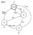
Figure 2 shows a state diagram of the operating states of a computer system in accordance with an embodiment of the present invention. -
Figure 1 shows a schematic representation of acomputer system 1. Thecomputer system 1 comprises apower supply unit 2 and asystem board 3 electrically connected to thepower supply unit 2. - The
power supply unit 2 comprises one or more AC/DC converters 4, such as a main converter and an auxiliary converter. The AC/DC converters 4 may be implemented, for example, as one or more switched mode power supplies. For efficient control of thepower supply unit 2, in the described embodiment, amicrocontroller 5 may selectively activate and deactivate and/or configure each AC/DC converter 4 to provide one or more secondary supply voltages Vcc and one or more auxiliary voltages Vaux. - In alternative embodiments, only a singly DC supply voltage may be provided to a computer system. In particular, external AC adapter converting an AC supply voltage into a single DC supply voltage may be used. In this case, an auxiliary voltage Vaux and/or a secondary control voltage Vcc may be generated based on the single DC voltage by circuitry arranged on the
system board 3. Furthermore, somecomputer systems 1 may have an AC/DC converter circuit arranged directly on thesystem board 3 for providing an auxiliary voltage Vaux and/or a secondary control voltage Vcc directly from an AC supply voltage - Referring back to the embodiment shown in
Figure 1 , themicrocontroller 5 may monitor the proper operation of the AC/DC converter 4 and provide a corresponding control signal, often referred to as a power good signal, PGPSU, via a correspondingcontrol signal output 8. In particular, it may provide the power good signal after the voltage at a supply voltage terminal 6 has exceeded a predefined voltage level. Furthermore, thepower supply unit 2 comprises a control signal input 9 for receiving a control signal Son for selectively switching thepower supply unit 2 from a standby mode into a normal operating mode, and vice versa. In the standby mode, thepower supply unit 2 will only provide the auxiliary voltage Vaux through anauxiliary voltage terminal 7. In the normal operating mode, thepower supply unit 2 will also provide the secondary supply voltage Vcc at one or more supply voltage terminals 6. - In the embodiment shown in
Figure 1 , thesystem board 3 comprises aCPU 10, afirmware component 11, achipset 12, asequencing microcontroller 13, avoltage comparator 14, and avoltage regulator 15. In a normal operation of thecomputer system 1, theCPU 10 and further components of thesystem board 3 not shown inFigure 1 are operated with the secondary supply voltage Vcc, either directly or indirectly. In case of theCPU 10, the secondary supply voltage Vcc of for example 12, 5 or 3.3 V may be further converted by thevoltage regulator 15 to fit the input requirements of theCPU 10. For example, a secondary supply voltage Vcc of 12 V may be converted by a DC converter to an input voltage VCPU of the CPU of 1.5, 1.25 or 1.1 V. - At least some of the components of the
system board 3 are connected to the auxiliary voltage Vaux. For example, certain components of thechipset 12 required for reactivating thecomputer system 1 from a standby or electronically switched off state are provided with the auxiliary voltage Vaux whenever thepower supply unit 2 is connected to an AC supply voltage VAC. In the embodiment shown inFigure 1 , in addition to parts of thechipset 12, thesequencing microcontroller 13 is also connected to the auxiliary voltage Vaux. Thesequencing microcontroller 13 is configured to selectively activate and deactivate further components of thesystem board 3. For example, thesequencing microcontroller 13 may directly interrupt the provision of the secondary supply voltage Vcc or the auxiliary voltage Vaux selectively to thecomponents sequencing microcontroller 13 by means of predetermined control signals. - It is noted that
Figure 1 is merely a schematic representation of anexemplary computer system 1. It only shows components relevant for the understanding of the present invention. In practice, a computer system may comprise any number of power supply units, system boards and components arranged on the system board. For example, in a server computer system, a number of redundant power supply units may be used to supply a single system board having a plurality of CPUs. Furthermore, some components shown as separate entities inFigure 1 may be integrated with one another. For example, thefirmware component 11 and thechipset 12 may be integrated into a single component. Inversely, in particular thechipset 12 may be embodied in a number of functionally and physically separate components. Furthermore, thevoltage comparator 14 andvoltage regulator 15 may be integrated. However, at least in some embodiments, thevoltage comparator 14 or thevoltage regulator 15 may not be present at all. For example, if thepower supply unit 2 provides a power good signal PGPSU to thesequencing microcontroller 13, the provision of anadditional voltage comparator 14 on thesystem board 3 may not be necessary. Furthermore, if thepower supply unit 2 provides a secondary supply voltage Vcc appropriate for theCPU 10, the provision of avoltage regulator 15 will not be necessary. - In the following, the operation of the
computer system 1 in accordance withFigure 1 will be described with respect to the state diagram ofFigure 2 . - According to one aspect of the invention, a "never off" feature is implemented in the
computer system 1. By activating a corresponding firmware setting in a setup dialogue of a BIOS program stored in thefirmware component 11, a user can set thecomputer system 1 to activate the "never off" feature. Activating "never off" feature results in a rebooting of thesystem board 3 after detecting a shutdown of thesystem board 3. Therefore thecomputer system 1 cannot be switched off by a user or a software for a period longer than the time required for rebooting. - If the "never off" feature of the
computer system 1 is set as active, the BIOS program stored in thefirmware component 11 configures thechipset 12 to send a NEVER_OFF_H control signal to a input pin of thesequencing controller 13. Otherwise, this signal is deasserted. - If the
chipset 12 sends the NEVER_OFF_H signal to the input pin of thesequencing microcontroller 13, thesequencing microcontroller 13 monitors the Son mode control signal to detect a shutdown of thesystem board 3. In other embodiments thesequencing microcontroller 13 monitors another signal, like a VCC secondary supply voltage to detect a shutdown of thesystem board 3. - If the
sequencing microcontroller 13 detects a shutdown of thesystem board 3, thesequencing microcontroller 13 sends a BTN_PWR_DEEPS5_L signal to a power button pin BTN_PWR_PCH_L of thechipset 12 to reboot thesystem board 3 and therefore restart and reactivate thecomputer system 1. - After sending the BTN_PWR_DEEPS5_L signal to the
chipset 12, thesequencing microcontroller 13 monitors control signals of thechipset 12. By monitoring the control signals of thechipset 12, thesequencing microcontroller 13 can detect failures in rebooting of thesystem board 3. Thesequencing microcontroller 13 resends the BTN_PWR_DEEPS5_L signal to thechipset 12 after time intervals of 3000 milliseconds until the control signals of thechipset 12 indicate that the reboot of thesystem board 3 is successful. Of course the time interval can have other values. For example the time interval can be chosen longer. - Additionally the
computer system 1 can be provided with an AC failure recognition. Upon first connection of thecomputer system 1 to the AC supply voltage VAC, thecomputer system 1 in general and thesequencing microcontroller 13 in particular enter a so-calledAC failure state 20. TheAC failure state 20 may be detected, for example, by the provision of an auxiliary voltage Vaux to thesequencing microcontroller 13 after a previous interruption of the auxiliary voltage Vaux. - In this context, it should be noted that not all interruptions of a primary AC supply voltage VAC necessarily lead to an interruption of the secondary auxiliary voltage Vaux. In particular, typically
power supply units 2 comprise one or more buffering capacitors or other energy storage elements, which may provide the auxiliary voltage Vaux for a predetermined period of time after a failure of the AC supply voltage VAC. For example, in apower supply unit 2 typically used in a server system, the auxiliary voltage Vaux may be provided for a time of roughly 30 seconds after a primary supply voltage VAC has been interrupted. - A detection of an AC failure results in the generation of a corresponding control signal after the
power supply unit 2 is reconnected to the AC supply voltage VAC. For this purpose, in the embodiment shown inFigure 1 , thesequencing microcontroller 13 provides a failure signal Sfail to thechipset 12 and/or thefirmware component 11. - After a predetermined waiting period, the
sequencing microcontroller 13 may provide the auxiliary voltage Vaux to thechipset 12. In response to the provision of the auxiliary voltage Vaux, thechipset 12 will be initialized and thecomputer system 1 will enter apredefined standby mode 21. In the diagram ofFigure 2 , thecomputer system 1 enters the ACPI standby state S5. Alternatively, thecomputer system 1 may enter the ACPI suspend state S3. In case the auxiliary voltage Vaux should fail in thestandby mode 21, thecomputer system 1 returns to theAC failure state 20. - If the power is not interrupted, after an optional waiting time, the
chipset 12 may issue a control signal Son to themicrocontroller 5 to activate the provision of the secondary supply voltage Vcc. Alternatively, the activation of thepower supply unit 2 may also be requested by thesequencing microcontroller 13. As a result, thecomputer system 1 changes into aninitialization state 22. In response to the control signal Son, themicrocontroller 5 activates or reconfigures the AC/DC converter 4 to provide the secondary supply voltage Vcc in addition to the auxiliary voltage Vaux. - In the
initialization state 22, thechipset 12 will wait for the provision of a so-called power good signal either from thepower supply unit 2, thecomparator 14, or both. However, in case a further interruption of the AC supply voltage VAC occurs at this state, thepower supply unit 2 may not be able to provide the requested secondary supply voltage Vcc such that thecomputer system 1 cannot continue its initialization procedure. - In order to detect and avoid a deadlock situation, the
sequencing microcontroller 13 actively monitors both the mode control signal Son provided to thepower supply unit 5 as well as the power good signals PGPSU and PGVC, provided by thepower supply unit 2 and thevoltage comparator 14, respectively. In particular, after the activation of thepower supply unit 2 has been requested using the control signal Son, thesequencing microcontroller 13 starts a timer, which will time out after a predetermined period of time Tmax, for example 500 milliseconds. Normally, this should be sufficient for thepower supply unit 2 to provide the requested secondary supply voltage Vcc. - However, in case of a further AC failure, either the control signal PGPSU or the control signal PGVC will not be provided within the predetermined time period. In this way, the
sequencing microcontroller 13 will detect the occurrence of the AC failure during the start of thepower supply unit 2. In response, thesequencing microcontroller 13 will signal the occurrence of a failure, in particular a failure of the AC supply voltage VAC, to other components of thesystem board 3. In particular, thesequencing microcontroller 13 may again provide the failure signal Sfail to thechipset 12 and return to the AC failstate 20. - The failure of the AC supply voltage VAC may be signaled in different ways. According to a first embodiment, the
sequencing microcontroller 13 will interrupt the auxiliary supply voltage Vaux to all components connected to thesequencing microcontroller 13. In particular, thechipset 12 will be disconnected from the auxiliary voltage Vaux for a predetermined period of time resulting in a full system reset. In response to such an interruption of the auxiliary voltage Vaux, thechipset 12 will start its initialization sequence again. Alternatively, in case thechipset 12 is connected to the auxiliary voltage Vaux directly, thesequencing microcontroller 13 may provide an appropriate control signal, for example a resume-reset signal to thechipset 12. This signal will be asserted and de-asserted after a predetermined amount of time to actively request a re-initialization of thechipset 12 and potentially further components of thesystem board 3. - In case a further power outage of the
power supply unit 2 should occur during the subsequent initialization phase, thesequencing microcontroller 13 will again signal an AC failure, such that no deadlock situation will arise. Assuming that the primary AC supply voltage VAC eventually becomes stable, thechipset 12 and other components of thesystem board 3 will finally proceed with a normal initialization process. In particular, both thepower supply unit 2 and thevoltage comparator 14 will generate a respective power good signal PGPSU and PGVC within the predetermined period of time Tmax from the provision of the mode control signal Son. In response, the computer system enters anormal operating mode 23, in particular the ACPI S0 state, in which theCPU 10 becomes operational. - Accordingly, the
firmware components 11 will start executing so-called BIOS code on theCPU 10. During the execution of the BIOS code, due to assertion of an appropriate control signal through thesequencing microcontroller 13 or thechipset 12, theBIOS component 11 will be made aware of the occurrence of the previous AC failure. In response to a corresponding BIOS setting, the BIOS code of thefirmware components 11 may instruct thecomputer system 1 to remain in the operatingmode 23, i.e. the ACPI S0 state, or to return to thestandby mode 21, e.g. either the ACPI S3 or S5 state. For example, if thecomputer system 1 is configured to enter the ACPI S5 state after the occurrence of an AC failure, a corresponding mode change back to thestandby mode 21 may be requested by de-asserting the mode control signal Son. - As indicated in
Figure 2 , in thenormal operating mode 23, thesequencing microcontroller 13 keeps monitoring one or both power good signals PGPSU and PGVC. In case one or both of the power good signals should fail, the system returns to the AC failstate 20. - In effect, by monitoring the control signals PGPSU, PGVC and/or Son provided by the
power supply unit 2 and components of thesystem board 3, thesequencing microcontroller 13 can detect the occurrence of AC power failure in all operating states of thecomputer system 1, including aninitialization state 22. By signaling the detection of an AC failure to other components of thesystem board 3, in particular thechipset 12, even short AC power failures, which may not lead to an interruption of the auxiliary voltage Vaux, can be detected by all components, ensuring that the components of thesystem board 3 can be brought into a well-defined state. This is of particular importance for remotely installed computer systems, where a manual re-initialization is either impossible or very costly. -
- 1
- computer system
- 2
- power supply unit
- 3
- system board
- 4
- AC/DC converter
- 5
- microcontroller
- 6
- supply voltage terminal
- 7
- auxiliary voltage terminal
- 8
- control signal output
- 9
- control signal input
- 10
- CPU
- 11
- firmware component
- 12
- chipset
- 13
- sequencing microcontroller
- 14
- voltage comparator
- 15
- voltage regulator
- 20
- AC failure state
- 21
- standby mode
- 22
- initialization state
- 23
- normal operating mode
- PGPSU
- power good signal (of the PSU)
- PGVC
- power good signal (of the system board)
- Sfail
- failure signal
- Son
- mode control signal
- Tmax
- predetermined time period
- VAC
- AC supply voltage
- Vaux
- auxiliary voltage
- Vcc
- secondary supply voltage
- NEVER_OFF_H
- never off signal
- BTN_PWR_DEEPS5_L
- power signal
Claims (15)
- Computer system (1), comprising- a power supply unit (2) for generating at least one DC supply voltage (Vcc, Vaux) based on an AC supply voltage (VAC), and- a system board (3) electrically connected to the power supply unit (2), the system board (3) comprising a sequencing microcontroller (13) for selectively activating further components of the system board (3), the further components comprising a chipset (12), wherein the sequencing microcontroller (13) is configured to monitor the state of at least one control signal of the power supply unit (2) and/or the system board (3) to detect a shutdown and a successful reboot of the system board (3) and, after a shutdown of the system board (3) is detected, to signal a reboot command to at least the chipset (12) at predetermined intervals until a successful reboot of the system board (3) is detected.
- The computer system (1) according to claim 1, wherein the further components comprise a firmware component (11) configured to activate a predetermined operating mode (21, 23) of the computer system (1) in accordance with a stored firmware setting after a shutdown of the system board (3) is detected.
- The computer system (1) according to claim 1 or 2, wherein the sequencing microcontroller (13) is further configured to detect a failure of the AC supply voltage (VAC) and to signal the failure of the AC supply voltage (VAC) to at least the chipset (12).
- The computer system (1) according to claim 3, wherein the sequencing microcontroller (13) is configured to selectively provide the at least one DC supply voltage (Vcc, Vaux) to the further components of the system board (3) and to interrupt the provision of the at least one DC supply voltage (Vcc, Vaux) to all further components of the system board (3) for a predetermined period of time to signal the failure of the AC supply voltage (VAC).
- The computer system (1) according to claim 3, wherein the sequencing microcontroller (13) is configured to provide a resume-reset control signal to the chipset (12) for a predetermined amount of time to signal the failure of the AC supply voltage (VAC).
- The computer system (1) according to any one of the claims 3 to 5, wherein the further components comprise a firmware component (11) configured to activate a predetermined operating mode (21, 23) of the computer system (1) after a power failure in accordance with a stored firmware setting, wherein the sequencing microcontroller (13) is further configured to provide a failure signal (Sfail) to the firmware component (11) to signal the failure of the AC supply voltage (VAC).
- The computer system (1) according to any one of claims 1 to 6, wherein the power supply unit (2) is configured for generating at least one secondary supply voltage (Vcc) and at least one auxiliary voltage (Vaux) and the sequencing microcontroller (13) is configured to monitor at least mode control signal (Son) provided by the chipset (12) for a request to enter a predefined operating mode (21, 23) of the computer system (1), to activate a timer in response to the detection of a request to enter the predefined operating mode, to monitor the provision of the secondary supply voltage (Vcc) from the power supply unit (2) to the system board (3), and to signal a failure of the AC supply voltage (VAC) if the provision of the secondary supply voltage (Vcc) is not detected within a predetermined period of time (Tmax).
- The computer system (1) according to claim 7, wherein the sequencing microcontroller (13) is configured to monitor at least one of the following control signals: a first power good signal (PGPSU) provided by the power supply unit (2) indicating that the secondary supply voltage (Vcc) at an output terminal (6) of the power supply unit (2) has reached a first predefined voltage level and a second power good signal (PGVC) provided by a voltage comparator (14) of the system board (3) indicating that the secondary supply voltage (Vcc) at a supply line of the system board (3) has reached a second predefined voltage level.
- A method of operating a computer system (1), the computer system (1) comprising a power supply unit (2) and a system board (3) electrically connected to the power supply unit (2), the system board (3) comprising a sequencing microcontroller (13) and a chipset (12), wherein the sequencing microcontroller (13) performs the following steps:- detecting a shutdown of the system board (3);- if a shutdown was detected, signaling a reboot command to at least the chipset (12) and activating a first timer;- monitoring at least one control signal provided by the chipset (12) to determine if the rebooting of the system board (13) was successful and deactivating the first timer if the monitored control signal indicates that the rebooting of the system board (3) was successful; and- resending the reboot command, if the activated first timer reaches a predetermined value.
- The method in accordance with claim 9, wherein the sequencing microcontroller (13) additionally performs the following steps:- detecting a connection of the power supply unit (2) to an AC supply voltage (VAC);- activating a second timer in response to a request to enter a predefined operating mode (21, 23) of the computer system (1);- monitoring at least one power good signal (PGPSU, PGVC) for at least a predetermined period of time (Tmax);- signaling a failure of the AC supply voltage (VAC) to at least the chipset (12) if the at least one power good signal (PGPSU, PGVC) is not received within the predetermined period of time (Tmax) from the request to enter the predefined operating mode (21, 23) of the computer system (1).
- The method in accordance with claim 10, wherein the steps of activating the second timer and monitoring the at least one power good signal (PGPSU, PGVC) are performed during an initialization state (22) of the computer system (1).
- The method in accordance with any one of the claims 10 to 11, wherein the sequencing microcontroller (13) further performs the following steps:- continuously monitoring the at least power good signal (PGPSU, PGVC) during a normal operation mode (23) of the computer system; and- signaling a failure of the AC supply voltage (VAC) to at least the chipset (12) if the at least one power good signal (PGPSU, PGVC) is deactivated in the normal operation mode (23) of the computer system (1).
- The method in accordance with any one of the claims 10 to 12, wherein in the step of detecting the connection of the power supply unit (2) to an AC supply voltage (VAC), the sequencing microcontroller (13) detects the provision of a previously absent auxiliary voltage (Vaux) from the power supply unit (2) indicative of the connection of the power supply unit (2) to the AC supply voltage (VAC).
- The method in accordance with any one of claims 10 to 13, wherein the sequencing microcontroller (13) provides the auxiliary voltage (Vaux) to the chipset (12) after the detection of the connection of the power supply unit (2) and wherein the step of signaling the failure of the AC supply voltage (VAC) comprises interrupting the provision of a DC supply voltage (Vcc, Vaux) to the chipset (12) of the system board (3) for a predetermined amount of time to signal the failure of the AC supply voltage (VAC).
- The method in accordance with one of claims 10 to 14, wherein the step of signaling the failure of the AC supply voltage (VAC) comprises providing a resume-reset control signal from the sequencing microcontroller (13) to the chipset (12) for a predetermined amount of time to signal the failure of the AC supply voltage (VAC).
Priority Applications (3)
| Application Number | Priority Date | Filing Date | Title |
|---|---|---|---|
| EP14161546.8A EP2924538B1 (en) | 2014-03-25 | 2014-03-25 | Computer system and method for its operation |
| US14/533,441 US10025595B2 (en) | 2014-03-25 | 2014-11-05 | Computer system and operating method |
| JP2014226767A JP5976074B2 (en) | 2014-03-25 | 2014-11-07 | Computer system and operation method thereof |
Applications Claiming Priority (1)
| Application Number | Priority Date | Filing Date | Title |
|---|---|---|---|
| EP14161546.8A EP2924538B1 (en) | 2014-03-25 | 2014-03-25 | Computer system and method for its operation |
Publications (2)
| Publication Number | Publication Date |
|---|---|
| EP2924538A1 true EP2924538A1 (en) | 2015-09-30 |
| EP2924538B1 EP2924538B1 (en) | 2020-06-17 |
Family
ID=50389832
Family Applications (1)
| Application Number | Title | Priority Date | Filing Date |
|---|---|---|---|
| EP14161546.8A Not-in-force EP2924538B1 (en) | 2014-03-25 | 2014-03-25 | Computer system and method for its operation |
Country Status (3)
| Country | Link |
|---|---|
| US (1) | US10025595B2 (en) |
| EP (1) | EP2924538B1 (en) |
| JP (1) | JP5976074B2 (en) |
Families Citing this family (5)
| Publication number | Priority date | Publication date | Assignee | Title |
|---|---|---|---|---|
| CN108029085B (en) | 2015-09-18 | 2021-03-30 | 夏普株式会社 | Terminal device, base station device, and communication method |
| US9958277B1 (en) * | 2015-12-18 | 2018-05-01 | EMC IP Holding Company LLC | Waypoint-assisted navigation of an enterprise facility |
| DE102018103286B4 (en) | 2018-02-14 | 2019-09-12 | Fujitsu Technology Solutions Intellectual Property Gmbh | Computer system, operating method for a microcontroller and computer program product |
| CN113865587A (en) | 2020-06-30 | 2021-12-31 | 伊姆西Ip控股有限责任公司 | Method, electronic device and computer program product for monitoring a field device |
| CN113868102A (en) | 2020-06-30 | 2021-12-31 | 伊姆西Ip控股有限责任公司 | Method, electronic device and computer program product for displaying information |
Citations (4)
| Publication number | Priority date | Publication date | Assignee | Title |
|---|---|---|---|---|
| US20030204709A1 (en) * | 2002-04-29 | 2003-10-30 | Daniel A. Rich | Method and /or apparatus for reliably booting a computer system |
| US6775784B1 (en) * | 1999-10-25 | 2004-08-10 | Samsung Electronics Co., Ltd. | Power supply control circuit and method for cutting off unnecessary power to system memory in the power-off state |
| WO2010087855A1 (en) * | 2009-01-30 | 2010-08-05 | Hewlett-Packard Development Company, L.P. | Computer system powered-off state auxiliary power rail control |
| US20130113532A1 (en) * | 2011-11-04 | 2013-05-09 | Wistron Corp. | Processing system and power control device thereof |
Family Cites Families (18)
| Publication number | Priority date | Publication date | Assignee | Title |
|---|---|---|---|---|
| JP3065683B2 (en) | 1991-03-20 | 2000-07-17 | 三菱レイヨン株式会社 | Prepreg |
| US5428252A (en) | 1992-01-03 | 1995-06-27 | Zilog, Inc. | Power supply interruption detection and response system for a microcontroller |
| JP2962387B2 (en) | 1993-05-07 | 1999-10-12 | 三菱電機株式会社 | Programmable controller and method for resetting specific other station in distributed control system using same, method for detecting cause of reset of other station, method for monitoring abnormal station, method for synchronously starting and method for synchronously stopping |
| US5511204A (en) | 1994-09-07 | 1996-04-23 | International Business Machines Corporation | Performing system tasks at power-off using system management interrupt |
| TW387584U (en) * | 1998-06-10 | 2000-04-11 | Winbond Electronics Corp | Controlling circuit used for computer power recovery and on off switch |
| US6274949B1 (en) * | 1999-01-18 | 2001-08-14 | Hewlett-Packard Company | Back-up power accessory for a computer |
| JP2000267767A (en) | 1999-03-19 | 2000-09-29 | Fujitsu General Ltd | Online system |
| US6367022B1 (en) | 1999-07-14 | 2002-04-02 | Visteon Global Technologies, Inc. | Power management fault strategy for automotive multimedia system |
| JP2005141623A (en) | 2003-11-10 | 2005-06-02 | Matsushita Electric Works Ltd | Terminal control device corresponding to instantaneous power failure and terminal control system |
| US20060136765A1 (en) | 2004-12-03 | 2006-06-22 | Poisner David L | Prevention of data loss due to power failure |
| JP4531020B2 (en) | 2006-08-01 | 2010-08-25 | ルネサスエレクトロニクス株式会社 | Semiconductor integrated circuit |
| JP2010079778A (en) | 2008-09-29 | 2010-04-08 | Nec Personal Products Co Ltd | Information processor, and method for displaying bios setting screen |
| TWI375912B (en) * | 2008-10-17 | 2012-11-01 | Asrock Inc | Method for reducing time of booting and computer system |
| US8627132B2 (en) * | 2008-12-31 | 2014-01-07 | Linear Technology Corporation | Autonomous multi-device event synchronization and sequencing technique eliminating master and slave assignments |
| JP2011039963A (en) | 2009-08-18 | 2011-02-24 | Toshiba Tec Corp | Electronic equipment, commodity sales data registration device, and control program of electronic equipment |
| JP5353762B2 (en) | 2010-02-26 | 2013-11-27 | ブラザー工業株式会社 | Memory control device |
| JP5455826B2 (en) | 2010-07-14 | 2014-03-26 | 萩原電気株式会社 | Power-on control circuit |
| JP5174093B2 (en) | 2010-07-26 | 2013-04-03 | 東芝テック株式会社 | Electronic device and control program thereof |
-
2014
- 2014-03-25 EP EP14161546.8A patent/EP2924538B1/en not_active Not-in-force
- 2014-11-05 US US14/533,441 patent/US10025595B2/en active Active
- 2014-11-07 JP JP2014226767A patent/JP5976074B2/en not_active Expired - Fee Related
Patent Citations (4)
| Publication number | Priority date | Publication date | Assignee | Title |
|---|---|---|---|---|
| US6775784B1 (en) * | 1999-10-25 | 2004-08-10 | Samsung Electronics Co., Ltd. | Power supply control circuit and method for cutting off unnecessary power to system memory in the power-off state |
| US20030204709A1 (en) * | 2002-04-29 | 2003-10-30 | Daniel A. Rich | Method and /or apparatus for reliably booting a computer system |
| WO2010087855A1 (en) * | 2009-01-30 | 2010-08-05 | Hewlett-Packard Development Company, L.P. | Computer system powered-off state auxiliary power rail control |
| US20130113532A1 (en) * | 2011-11-04 | 2013-05-09 | Wistron Corp. | Processing system and power control device thereof |
Also Published As
| Publication number | Publication date |
|---|---|
| US10025595B2 (en) | 2018-07-17 |
| EP2924538B1 (en) | 2020-06-17 |
| JP2015185159A (en) | 2015-10-22 |
| JP5976074B2 (en) | 2016-08-23 |
| US20150277931A1 (en) | 2015-10-01 |
Similar Documents
| Publication | Publication Date | Title |
|---|---|---|
| US9317093B2 (en) | Computer system selectively directing power to a battery from either a backup power supply or a normal power supply based on a reduction of voltage measured from one or more detection circuits | |
| US10025595B2 (en) | Computer system and operating method | |
| EP2372491B1 (en) | Power lock-up setting method and electronic apparatus using the same | |
| KR101739501B1 (en) | A power saving method of a computer system | |
| CN111831488B (en) | TCMS-MPU control unit with safety level design | |
| US20130132757A1 (en) | Power-on controlling method and system thereof | |
| CN104182243B (en) | Sleep state control system, computer system and sleep state detection method thereof | |
| US6272630B1 (en) | Method and device for reserving wake-up functions of computer system after power loss | |
| JP5455826B2 (en) | Power-on control circuit | |
| US20070234124A1 (en) | Management function setting method for intelligent platform management interface | |
| US9411704B2 (en) | Computer systems and methods of detecting AC failure | |
| CN110389643B (en) | Server and remote control method thereof | |
| CN103135728B (en) | Power start control method and system thereof | |
| JP5740454B2 (en) | Computer system and computer system operation method for AC malfunction detection | |
| US10921875B2 (en) | Computer system, operational method for a microcontroller, and computer program product | |
| KR101746434B1 (en) | A method for blocking the stanby power having multiple sensing functions | |
| KR101351703B1 (en) | Terminal device and power control device | |
| JP6446948B2 (en) | Electronic device, power supply device and power supply monitoring method | |
| CN114647293A (en) | Power failure protection method and device, power supply monitoring assembly and server | |
| JP5422426B2 (en) | Information processing device | |
| KR20210012114A (en) | Switching mode power supply built-in standby power cut-off apparatus and method | |
| US20170269941A1 (en) | Method for forcibly resetting microcontroller | |
| JP5342801B2 (en) | Power supply control circuit, computer having the same, and power supply control method | |
| CN111381659A (en) | Computer system and power management method | |
| JP2011186662A (en) | Information processor |
Legal Events
| Date | Code | Title | Description |
|---|---|---|---|
| PUAI | Public reference made under article 153(3) epc to a published international application that has entered the european phase |
Free format text: ORIGINAL CODE: 0009012 |
|
| AK | Designated contracting states |
Kind code of ref document: A1 Designated state(s): AL AT BE BG CH CY CZ DE DK EE ES FI FR GB GR HR HU IE IS IT LI LT LU LV MC MK MT NL NO PL PT RO RS SE SI SK SM TR |
|
| AX | Request for extension of the european patent |
Extension state: BA ME |
|
| 17P | Request for examination filed |
Effective date: 20160324 |
|
| RBV | Designated contracting states (corrected) |
Designated state(s): AL AT BE BG CH CY CZ DE DK EE ES FI FR GB GR HR HU IE IS IT LI LT LU LV MC MK MT NL NO PL PT RO RS SE SI SK SM TR |
|
| STAA | Information on the status of an ep patent application or granted ep patent |
Free format text: STATUS: EXAMINATION IS IN PROGRESS |
|
| 17Q | First examination report despatched |
Effective date: 20180613 |
|
| GRAP | Despatch of communication of intention to grant a patent |
Free format text: ORIGINAL CODE: EPIDOSNIGR1 |
|
| STAA | Information on the status of an ep patent application or granted ep patent |
Free format text: STATUS: GRANT OF PATENT IS INTENDED |
|
| INTG | Intention to grant announced |
Effective date: 20200114 |
|
| GRAS | Grant fee paid |
Free format text: ORIGINAL CODE: EPIDOSNIGR3 |
|
| GRAA | (expected) grant |
Free format text: ORIGINAL CODE: 0009210 |
|
| STAA | Information on the status of an ep patent application or granted ep patent |
Free format text: STATUS: THE PATENT HAS BEEN GRANTED |
|
| AK | Designated contracting states |
Kind code of ref document: B1 Designated state(s): AL AT BE BG CH CY CZ DE DK EE ES FI FR GB GR HR HU IE IS IT LI LT LU LV MC MK MT NL NO PL PT RO RS SE SI SK SM TR |
|
| REG | Reference to a national code |
Ref country code: GB Ref legal event code: FG4D |
|
| REG | Reference to a national code |
Ref country code: CH Ref legal event code: EP |
|
| REG | Reference to a national code |
Ref country code: DE Ref legal event code: R096 Ref document number: 602014066613 Country of ref document: DE |
|
| REG | Reference to a national code |
Ref country code: IE Ref legal event code: FG4D |
|
| REG | Reference to a national code |
Ref country code: AT Ref legal event code: REF Ref document number: 1282137 Country of ref document: AT Kind code of ref document: T Effective date: 20200715 |
|
| PG25 | Lapsed in a contracting state [announced via postgrant information from national office to epo] |
Ref country code: FI Free format text: LAPSE BECAUSE OF FAILURE TO SUBMIT A TRANSLATION OF THE DESCRIPTION OR TO PAY THE FEE WITHIN THE PRESCRIBED TIME-LIMIT Effective date: 20200617 Ref country code: GR Free format text: LAPSE BECAUSE OF FAILURE TO SUBMIT A TRANSLATION OF THE DESCRIPTION OR TO PAY THE FEE WITHIN THE PRESCRIBED TIME-LIMIT Effective date: 20200918 Ref country code: NO Free format text: LAPSE BECAUSE OF FAILURE TO SUBMIT A TRANSLATION OF THE DESCRIPTION OR TO PAY THE FEE WITHIN THE PRESCRIBED TIME-LIMIT Effective date: 20200917 Ref country code: SE Free format text: LAPSE BECAUSE OF FAILURE TO SUBMIT A TRANSLATION OF THE DESCRIPTION OR TO PAY THE FEE WITHIN THE PRESCRIBED TIME-LIMIT Effective date: 20200617 Ref country code: LT Free format text: LAPSE BECAUSE OF FAILURE TO SUBMIT A TRANSLATION OF THE DESCRIPTION OR TO PAY THE FEE WITHIN THE PRESCRIBED TIME-LIMIT Effective date: 20200617 |
|
| REG | Reference to a national code |
Ref country code: LT Ref legal event code: MG4D |
|
| REG | Reference to a national code |
Ref country code: NL Ref legal event code: MP Effective date: 20200617 |
|
| PG25 | Lapsed in a contracting state [announced via postgrant information from national office to epo] |
Ref country code: HR Free format text: LAPSE BECAUSE OF FAILURE TO SUBMIT A TRANSLATION OF THE DESCRIPTION OR TO PAY THE FEE WITHIN THE PRESCRIBED TIME-LIMIT Effective date: 20200617 Ref country code: LV Free format text: LAPSE BECAUSE OF FAILURE TO SUBMIT A TRANSLATION OF THE DESCRIPTION OR TO PAY THE FEE WITHIN THE PRESCRIBED TIME-LIMIT Effective date: 20200617 Ref country code: BG Free format text: LAPSE BECAUSE OF FAILURE TO SUBMIT A TRANSLATION OF THE DESCRIPTION OR TO PAY THE FEE WITHIN THE PRESCRIBED TIME-LIMIT Effective date: 20200917 Ref country code: RS Free format text: LAPSE BECAUSE OF FAILURE TO SUBMIT A TRANSLATION OF THE DESCRIPTION OR TO PAY THE FEE WITHIN THE PRESCRIBED TIME-LIMIT Effective date: 20200617 |
|
| REG | Reference to a national code |
Ref country code: DE Ref legal event code: R084 Ref document number: 602014066613 Country of ref document: DE |
|
| REG | Reference to a national code |
Ref country code: AT Ref legal event code: MK05 Ref document number: 1282137 Country of ref document: AT Kind code of ref document: T Effective date: 20200617 |
|
| PG25 | Lapsed in a contracting state [announced via postgrant information from national office to epo] |
Ref country code: NL Free format text: LAPSE BECAUSE OF FAILURE TO SUBMIT A TRANSLATION OF THE DESCRIPTION OR TO PAY THE FEE WITHIN THE PRESCRIBED TIME-LIMIT Effective date: 20200617 Ref country code: AL Free format text: LAPSE BECAUSE OF FAILURE TO SUBMIT A TRANSLATION OF THE DESCRIPTION OR TO PAY THE FEE WITHIN THE PRESCRIBED TIME-LIMIT Effective date: 20200617 |
|
| PG25 | Lapsed in a contracting state [announced via postgrant information from national office to epo] |
Ref country code: PT Free format text: LAPSE BECAUSE OF FAILURE TO SUBMIT A TRANSLATION OF THE DESCRIPTION OR TO PAY THE FEE WITHIN THE PRESCRIBED TIME-LIMIT Effective date: 20201019 Ref country code: AT Free format text: LAPSE BECAUSE OF FAILURE TO SUBMIT A TRANSLATION OF THE DESCRIPTION OR TO PAY THE FEE WITHIN THE PRESCRIBED TIME-LIMIT Effective date: 20200617 Ref country code: IT Free format text: LAPSE BECAUSE OF FAILURE TO SUBMIT A TRANSLATION OF THE DESCRIPTION OR TO PAY THE FEE WITHIN THE PRESCRIBED TIME-LIMIT Effective date: 20200617 Ref country code: SM Free format text: LAPSE BECAUSE OF FAILURE TO SUBMIT A TRANSLATION OF THE DESCRIPTION OR TO PAY THE FEE WITHIN THE PRESCRIBED TIME-LIMIT Effective date: 20200617 Ref country code: EE Free format text: LAPSE BECAUSE OF FAILURE TO SUBMIT A TRANSLATION OF THE DESCRIPTION OR TO PAY THE FEE WITHIN THE PRESCRIBED TIME-LIMIT Effective date: 20200617 Ref country code: CZ Free format text: LAPSE BECAUSE OF FAILURE TO SUBMIT A TRANSLATION OF THE DESCRIPTION OR TO PAY THE FEE WITHIN THE PRESCRIBED TIME-LIMIT Effective date: 20200617 Ref country code: RO Free format text: LAPSE BECAUSE OF FAILURE TO SUBMIT A TRANSLATION OF THE DESCRIPTION OR TO PAY THE FEE WITHIN THE PRESCRIBED TIME-LIMIT Effective date: 20200617 Ref country code: ES Free format text: LAPSE BECAUSE OF FAILURE TO SUBMIT A TRANSLATION OF THE DESCRIPTION OR TO PAY THE FEE WITHIN THE PRESCRIBED TIME-LIMIT Effective date: 20200617 |
|
| PG25 | Lapsed in a contracting state [announced via postgrant information from national office to epo] |
Ref country code: PL Free format text: LAPSE BECAUSE OF FAILURE TO SUBMIT A TRANSLATION OF THE DESCRIPTION OR TO PAY THE FEE WITHIN THE PRESCRIBED TIME-LIMIT Effective date: 20200617 Ref country code: SK Free format text: LAPSE BECAUSE OF FAILURE TO SUBMIT A TRANSLATION OF THE DESCRIPTION OR TO PAY THE FEE WITHIN THE PRESCRIBED TIME-LIMIT Effective date: 20200617 Ref country code: IS Free format text: LAPSE BECAUSE OF FAILURE TO SUBMIT A TRANSLATION OF THE DESCRIPTION OR TO PAY THE FEE WITHIN THE PRESCRIBED TIME-LIMIT Effective date: 20201017 |
|
| REG | Reference to a national code |
Ref country code: DE Ref legal event code: R097 Ref document number: 602014066613 Country of ref document: DE |
|
| PLBE | No opposition filed within time limit |
Free format text: ORIGINAL CODE: 0009261 |
|
| STAA | Information on the status of an ep patent application or granted ep patent |
Free format text: STATUS: NO OPPOSITION FILED WITHIN TIME LIMIT |
|
| PG25 | Lapsed in a contracting state [announced via postgrant information from national office to epo] |
Ref country code: DK Free format text: LAPSE BECAUSE OF FAILURE TO SUBMIT A TRANSLATION OF THE DESCRIPTION OR TO PAY THE FEE WITHIN THE PRESCRIBED TIME-LIMIT Effective date: 20200617 |
|
| 26N | No opposition filed |
Effective date: 20210318 |
|
| PG25 | Lapsed in a contracting state [announced via postgrant information from national office to epo] |
Ref country code: SI Free format text: LAPSE BECAUSE OF FAILURE TO SUBMIT A TRANSLATION OF THE DESCRIPTION OR TO PAY THE FEE WITHIN THE PRESCRIBED TIME-LIMIT Effective date: 20200617 |
|
| PG25 | Lapsed in a contracting state [announced via postgrant information from national office to epo] |
Ref country code: MC Free format text: LAPSE BECAUSE OF FAILURE TO SUBMIT A TRANSLATION OF THE DESCRIPTION OR TO PAY THE FEE WITHIN THE PRESCRIBED TIME-LIMIT Effective date: 20200617 |
|
| REG | Reference to a national code |
Ref country code: CH Ref legal event code: PL |
|
| REG | Reference to a national code |
Ref country code: BE Ref legal event code: MM Effective date: 20210331 |
|
| PG25 | Lapsed in a contracting state [announced via postgrant information from national office to epo] |
Ref country code: IE Free format text: LAPSE BECAUSE OF NON-PAYMENT OF DUE FEES Effective date: 20210325 Ref country code: LU Free format text: LAPSE BECAUSE OF NON-PAYMENT OF DUE FEES Effective date: 20210325 Ref country code: LI Free format text: LAPSE BECAUSE OF NON-PAYMENT OF DUE FEES Effective date: 20210331 Ref country code: CH Free format text: LAPSE BECAUSE OF NON-PAYMENT OF DUE FEES Effective date: 20210331 |
|
| PG25 | Lapsed in a contracting state [announced via postgrant information from national office to epo] |
Ref country code: BE Free format text: LAPSE BECAUSE OF NON-PAYMENT OF DUE FEES Effective date: 20210331 |
|
| REG | Reference to a national code |
Ref country code: DE Ref legal event code: R081 Ref document number: 602014066613 Country of ref document: DE Owner name: FUJITSU CLIENT COMPUTING LIMITED, KAWASAKI-SHI, JP Free format text: FORMER OWNER: FUJITSU TECHNOLOGY SOLUTIONS INTELLECTUAL PROPERTY GMBH, 80807 MUENCHEN, DE Ref country code: DE Ref legal event code: R081 Ref document number: 602014066613 Country of ref document: DE Owner name: FUJITSU TECHNOLOGY SOLUTIONS GMBH, DE Free format text: FORMER OWNER: FUJITSU TECHNOLOGY SOLUTIONS INTELLECTUAL PROPERTY GMBH, 80807 MUENCHEN, DE |
|
| PGFP | Annual fee paid to national office [announced via postgrant information from national office to epo] |
Ref country code: FR Payment date: 20230320 Year of fee payment: 10 |
|
| REG | Reference to a national code |
Ref country code: GB Ref legal event code: 732E Free format text: REGISTERED BETWEEN 20230413 AND 20230419 |
|
| PG25 | Lapsed in a contracting state [announced via postgrant information from national office to epo] |
Ref country code: HU Free format text: LAPSE BECAUSE OF FAILURE TO SUBMIT A TRANSLATION OF THE DESCRIPTION OR TO PAY THE FEE WITHIN THE PRESCRIBED TIME-LIMIT; INVALID AB INITIO Effective date: 20140325 |
|
| PGFP | Annual fee paid to national office [announced via postgrant information from national office to epo] |
Ref country code: GB Payment date: 20230323 Year of fee payment: 10 Ref country code: DE Payment date: 20230320 Year of fee payment: 10 |
|
| PG25 | Lapsed in a contracting state [announced via postgrant information from national office to epo] |
Ref country code: CY Free format text: LAPSE BECAUSE OF FAILURE TO SUBMIT A TRANSLATION OF THE DESCRIPTION OR TO PAY THE FEE WITHIN THE PRESCRIBED TIME-LIMIT Effective date: 20200617 |
|
| REG | Reference to a national code |
Ref country code: DE Ref legal event code: R081 Ref document number: 602014066613 Country of ref document: DE Owner name: FUJITSU CLIENT COMPUTING LIMITED, KAWASAKI-SHI, JP Free format text: FORMER OWNER: FUJITSU TECHNOLOGY SOLUTIONS GMBH, 80807 MUENCHEN, DE |
|
| REG | Reference to a national code |
Ref country code: GB Ref legal event code: 732E Free format text: REGISTERED BETWEEN 20231221 AND 20231222 |
|
| PG25 | Lapsed in a contracting state [announced via postgrant information from national office to epo] |
Ref country code: MK Free format text: LAPSE BECAUSE OF FAILURE TO SUBMIT A TRANSLATION OF THE DESCRIPTION OR TO PAY THE FEE WITHIN THE PRESCRIBED TIME-LIMIT Effective date: 20200617 |
|
| PG25 | Lapsed in a contracting state [announced via postgrant information from national office to epo] |
Ref country code: MT Free format text: LAPSE BECAUSE OF FAILURE TO SUBMIT A TRANSLATION OF THE DESCRIPTION OR TO PAY THE FEE WITHIN THE PRESCRIBED TIME-LIMIT Effective date: 20200617 |
|
| REG | Reference to a national code |
Ref country code: DE Ref legal event code: R119 Ref document number: 602014066613 Country of ref document: DE |
|
| GBPC | Gb: european patent ceased through non-payment of renewal fee |
Effective date: 20240325 |
|
| PG25 | Lapsed in a contracting state [announced via postgrant information from national office to epo] |
Ref country code: DE Free format text: LAPSE BECAUSE OF NON-PAYMENT OF DUE FEES Effective date: 20241001 |
|
| PG25 | Lapsed in a contracting state [announced via postgrant information from national office to epo] |
Ref country code: GB Free format text: LAPSE BECAUSE OF NON-PAYMENT OF DUE FEES Effective date: 20240325 |
|
| PG25 | Lapsed in a contracting state [announced via postgrant information from national office to epo] |
Ref country code: FR Free format text: LAPSE BECAUSE OF NON-PAYMENT OF DUE FEES Effective date: 20240331 |
|
| PG25 | Lapsed in a contracting state [announced via postgrant information from national office to epo] |
Ref country code: GB Free format text: LAPSE BECAUSE OF NON-PAYMENT OF DUE FEES Effective date: 20240325 Ref country code: FR Free format text: LAPSE BECAUSE OF NON-PAYMENT OF DUE FEES Effective date: 20240331 Ref country code: DE Free format text: LAPSE BECAUSE OF NON-PAYMENT OF DUE FEES Effective date: 20241001 |
|
| PG25 | Lapsed in a contracting state [announced via postgrant information from national office to epo] |
Ref country code: TR Free format text: LAPSE BECAUSE OF FAILURE TO SUBMIT A TRANSLATION OF THE DESCRIPTION OR TO PAY THE FEE WITHIN THE PRESCRIBED TIME-LIMIT Effective date: 20200617 |