EP2923839A1 - Liquid ejection apparatus and a method for producing liquid ejection apparatus - Google Patents
Liquid ejection apparatus and a method for producing liquid ejection apparatus Download PDFInfo
- Publication number
- EP2923839A1 EP2923839A1 EP15160852.8A EP15160852A EP2923839A1 EP 2923839 A1 EP2923839 A1 EP 2923839A1 EP 15160852 A EP15160852 A EP 15160852A EP 2923839 A1 EP2923839 A1 EP 2923839A1
- Authority
- EP
- European Patent Office
- Prior art keywords
- laminated body
- electrode
- communication opening
- ejection apparatus
- layer
- Prior art date
- Legal status (The legal status is an assumption and is not a legal conclusion. Google has not performed a legal analysis and makes no representation as to the accuracy of the status listed.)
- Granted
Links
Images



Classifications
-
- B—PERFORMING OPERATIONS; TRANSPORTING
- B41—PRINTING; LINING MACHINES; TYPEWRITERS; STAMPS
- B41J—TYPEWRITERS; SELECTIVE PRINTING MECHANISMS, i.e. MECHANISMS PRINTING OTHERWISE THAN FROM A FORME; CORRECTION OF TYPOGRAPHICAL ERRORS
- B41J2/00—Typewriters or selective printing mechanisms characterised by the printing or marking process for which they are designed
- B41J2/005—Typewriters or selective printing mechanisms characterised by the printing or marking process for which they are designed characterised by bringing liquid or particles selectively into contact with a printing material
- B41J2/01—Ink jet
- B41J2/135—Nozzles
- B41J2/14—Structure thereof only for on-demand ink jet heads
- B41J2/14201—Structure of print heads with piezoelectric elements
-
- B—PERFORMING OPERATIONS; TRANSPORTING
- B41—PRINTING; LINING MACHINES; TYPEWRITERS; STAMPS
- B41J—TYPEWRITERS; SELECTIVE PRINTING MECHANISMS, i.e. MECHANISMS PRINTING OTHERWISE THAN FROM A FORME; CORRECTION OF TYPOGRAPHICAL ERRORS
- B41J2/00—Typewriters or selective printing mechanisms characterised by the printing or marking process for which they are designed
- B41J2/005—Typewriters or selective printing mechanisms characterised by the printing or marking process for which they are designed characterised by bringing liquid or particles selectively into contact with a printing material
- B41J2/01—Ink jet
- B41J2/135—Nozzles
- B41J2/14—Structure thereof only for on-demand ink jet heads
- B41J2/14201—Structure of print heads with piezoelectric elements
- B41J2/14233—Structure of print heads with piezoelectric elements of film type, deformed by bending and disposed on a diaphragm
-
- B—PERFORMING OPERATIONS; TRANSPORTING
- B41—PRINTING; LINING MACHINES; TYPEWRITERS; STAMPS
- B41J—TYPEWRITERS; SELECTIVE PRINTING MECHANISMS, i.e. MECHANISMS PRINTING OTHERWISE THAN FROM A FORME; CORRECTION OF TYPOGRAPHICAL ERRORS
- B41J2/00—Typewriters or selective printing mechanisms characterised by the printing or marking process for which they are designed
- B41J2/005—Typewriters or selective printing mechanisms characterised by the printing or marking process for which they are designed characterised by bringing liquid or particles selectively into contact with a printing material
- B41J2/01—Ink jet
- B41J2/135—Nozzles
- B41J2/16—Production of nozzles
- B41J2/1607—Production of print heads with piezoelectric elements
-
- B—PERFORMING OPERATIONS; TRANSPORTING
- B41—PRINTING; LINING MACHINES; TYPEWRITERS; STAMPS
- B41J—TYPEWRITERS; SELECTIVE PRINTING MECHANISMS, i.e. MECHANISMS PRINTING OTHERWISE THAN FROM A FORME; CORRECTION OF TYPOGRAPHICAL ERRORS
- B41J2/00—Typewriters or selective printing mechanisms characterised by the printing or marking process for which they are designed
- B41J2/005—Typewriters or selective printing mechanisms characterised by the printing or marking process for which they are designed characterised by bringing liquid or particles selectively into contact with a printing material
- B41J2/01—Ink jet
- B41J2/135—Nozzles
- B41J2/14—Structure thereof only for on-demand ink jet heads
- B41J2002/14459—Matrix arrangement of the pressure chambers
-
- B—PERFORMING OPERATIONS; TRANSPORTING
- B41—PRINTING; LINING MACHINES; TYPEWRITERS; STAMPS
- B41J—TYPEWRITERS; SELECTIVE PRINTING MECHANISMS, i.e. MECHANISMS PRINTING OTHERWISE THAN FROM A FORME; CORRECTION OF TYPOGRAPHICAL ERRORS
- B41J2/00—Typewriters or selective printing mechanisms characterised by the printing or marking process for which they are designed
- B41J2/005—Typewriters or selective printing mechanisms characterised by the printing or marking process for which they are designed characterised by bringing liquid or particles selectively into contact with a printing material
- B41J2/01—Ink jet
- B41J2/135—Nozzles
- B41J2/14—Structure thereof only for on-demand ink jet heads
- B41J2002/14491—Electrical connection
-
- B—PERFORMING OPERATIONS; TRANSPORTING
- B41—PRINTING; LINING MACHINES; TYPEWRITERS; STAMPS
- B41J—TYPEWRITERS; SELECTIVE PRINTING MECHANISMS, i.e. MECHANISMS PRINTING OTHERWISE THAN FROM A FORME; CORRECTION OF TYPOGRAPHICAL ERRORS
- B41J2202/00—Embodiments of or processes related to ink-jet or thermal heads
- B41J2202/01—Embodiments of or processes related to ink-jet heads
- B41J2202/20—Modules
Definitions
- the disclosure relates to a liquid ejection apparatus configured to eject liquid and a method for producing the liquid ejection apparatus.
- a known liquid ejection apparatus e.g., an inkjet head, is configured to eject ink from a plurality of nozzles.
- the inkjet head includes a channeled substrate and a reservoir formation substrate.
- the channeled substrate includes a plurality of pressure chambers and a communication portion that is shared by the pressure chambers and communicates with the pressure chambers.
- a laminated body including a plurality of layers is disposed at the upper surface of the channeled substrate.
- the laminated body includes a vibration plate covering the pressure chambers and a plurality of piezoelectric elements corresponding to the pressure chambers.
- a nozzles plate is disposed at a surface of the channeled substrate opposite to the laminated body, e.g., the lower surface of the channeled substrate.
- the nozzles plate has the nozzles configured to communicate with the pressure chambers in the channeled substrate.
- the reservoir formation substrate is disposed above the channeled substrate to cover the piezoelectric elements included in the laminated body.
- the reservoir formation substrate is bonded to the laminated body with an adhesive in an area outside the piezoelectric elements.
- the reservoir formation substrate includes a reservoir portion.
- the reservoir portion communicates with the communication portion of the channeled substrate, via a communication opening formed on the laminated body. Ink supplied in the communication portion of the channeled substrate from the reservoir portion is distributed to each of the pressure chambers.
- a liquid ejection apparatus includes a nozzle and a first channeled structure defining a first liquid channel that communicates with the nozzle.
- a communication opening connects the first liquid channel and a second liquid channel.
- a laminated body has a piezoelectric element and a metal layer, and a first portion of the laminated body is supported by the first channeled structure and a second portion extends over the first liquid channel and thus is not supported by the first channeled structure.
- the communication opening extends through the second portion of the laminated body such that the second portion surrounds the communication opening.
- the second portion of the laminated body includes the metal layer surrounding the communication opening.
- a portion of the laminated body around the communication opening partially faces an ink channel in the channeled substrate.
- the circumferentially facing portion is disposed around the communication opening without being supported by the channeled substrate.
- the circumferentially facing portion is susceptible to damages.
- the circumferentially facing portion is positioned around the communication opening, so that pressure of liquid flowing into the communication opening is applied to the circumferentially facing portion.
- shrinkage force of the adhesive may be applied to the circumferentially facing portion. Further, when the vibration plate is vibrated due to the driving of the piezoelectric elements, the vibration is applied to the circumferentially facing portion.
- One or more aspects of the disclosure includes preventing or reducing damages on a circumferentially facing portion that is disposed at a portion of a laminated body around a communication opening and faces or opposes a channel formed in a channeled structure.
- Fig. 1 is a plan view of a printer in an illustrative embodiment according to one or more aspects of the disclosure. Referring to Fig. 1 , general structures of an inkjet printer 1 will be described. The front, rear, left, and right sides of the printer 1 are defined as depicted in Fig. 1 . The front or near side and the back side of the sheet of Fig. 1 are defined as the top/upper side and the bottom/lower side of the printer 1, respectively.
- description will be made with reference to directions as defined above.
- the inkjet printer 1 includes a platen 2, a carriage 3, an inkjet head 4, a feeding mechanism 5, and a controller 6.
- a recording medium e.g., a recording sheet 100
- the carriage 3 is configured to reciprocate along two guide rails 10 and 11 in a scanning direction at a region opposing the platen 2.
- An endless belt 14 is connected to the carriage 3. As a carriage drive motor 15 drives the endless belt 14, the carriage 3 moves in the scanning direction.
- the inkjet head 4 is mounted on the carriage 3.
- the inkjet head 4 is configured to move together with the carriage 3 in the scanning direction.
- the inkjet head 4 is connected by tubes (not depicted) to a cartridge holder 7 on which ink cartridges 17 of four colors (e.g., black, yellow, cyan, and magenta) are mounted.
- the inkjet head 4 includes head units 12 and 13 arranged in the scanning direction.
- Each head unit 12 and 13 has a plurality of nozzles 24 (refer to Figs. 2-5D ) formed on the lower surface thereof (e.g., the back side of the sheet of Fig. 1 ).
- the nozzles 24 are configured to eject ink toward the recording sheet 100 placed on the platen 2.
- one head unit 12 is configured to eject black and yellow inks.
- the other head unit 13 is configured to eject cyan and magenta inks.
- the feeding mechanism 5 includes two feeding rollers 18 and 19 interposing the platen 2 therebetween in a sheet feeding direction.
- the feeding mechanism 5 is configured to feed the recording sheet 100 placed on the platen 2 in the sheet feeding direction with the two feeding rollers 18 and 19.
- the controller 6 includes a read only memory (ROM), a random access memory (RAM), and an application specific integrated circuit (ASIC) comprising various control circuits.
- the controller 6 is configured to execute various processing, e.g., printing onto the recording sheet 100, based on programs stored in the ROM, with the ASIC.
- the controller 6 controls, for example, the head units 12 and 13 of the inkjet head 4 and the carriage drive motor 15, based on a print instruction input from an external device, e.g., a personal computer (PC), to print, for example, an image, onto the recording sheet 100. More specifically, an ink ejection operation and a feeding operation are alternately performed.
- PC personal computer
- ink is ejected while the inkjet head 4 is moved together with the carriage 3 in the scanning direction.
- the feeding operation the recording sheet 100 is fed in the sheet feeding direction by a predetermined amount by the feeding rollers 18 and 19.
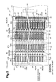
- Fig. 2 is a top view of the head unit 12 of the inkjet head 4.
- Fig. 3 is an enlarged view of a portion "X" of the head unit of Fig. 2 .
- Fig. 4A is a cross-sectional view of the head unit 12, taken along the line A-A of Fig. 3 .
- Fig. 4B is a cross-sectional view of the head unit 12, taken along the line B-B of Fig. 3 . As depicted in Figs.
- the head unit 12 includes a nozzles plate 20, a channeled member 21, a laminated body 22, and a reservoir formation member 23.
- a nozzles plate 20 a channeled member 21, a laminated body 22, and a reservoir formation member 23.
- a reservoir formation member 23 disposed above the channeled member 21 and the laminated body 22 is illustrated by chain double-dashed lines, for the sake of simplification of the drawings.
- the nozzles plate 20 is formed of, for example, metallic material, e.g., stainless steel, silicon, or synthetic resin material, e.g., polyimide. As depicted in Figs. 4A and 4B , the nozzles plate 20 has the nozzles 24.
- the nozzles 24 are arranged in the sheet feeding direction.
- the nozzles 24 constitute four nozzle rows 25 arranged in the scanning direction.
- Right two nozzle rows 25a are configured to eject black ink.
- Positions of the nozzles 24 of the two nozzle rows 25a are mutually deviated in the sheet feeding direction by a half of the alignment pitch P (P/2) for each nozzle row 25.
- Left two nozzle rows 25b are configured to eject yellow ink. Similar to the nozzle rows 25a for black ink, positions of the nozzles 24 of the two nozzle rows 25b for yellow ink are mutually deviated in the sheet feeding direction by a half pitch (P/2).
- the channeled member 21 is formed of silicon.
- the nozzles plate 20 is bonded to the lower surface of the channeled member 21.
- the channeled member 21 includes a plurality of pressure chambers 26 communicating with the corresponding nozzles 24.
- Each pressure chamber 26 has a rectangular planar shape elongated in the scanning direction.
- the pressure chambers 26 are arranged in the sheet feeding direction in association with the nozzles 24.
- the pressure chambers 26 constitute four pressure chamber rows 27 arranged in the scanning direction. Right two pressure chamber rows 27a are for black ink and left two pressure chamber rows 27b are for yellow ink.
- the laminated body 22 is configured to apply, to ink in the pressure chambers 26, ejection energy for ejecting ink from the respective nozzles 24.
- the laminated body 22 is disposed at the upper surface of the channeled member 21.
- the laminated body 22 is formed by laminating, for example, a vibration plate 30, a common electrode 31, a piezoelectric layer 32, an individual electrode 33, and a drive wiring 35, in layers.
- the laminated body 22 is formed by sequentially laminating a very thin layer of a few or a several ⁇ m by a known semiconductor process technique on the upper surface of a silicon substrate, which becomes the channeled member 21.
- the vibration plate 30 is disposed at the entire upper surface of the channeled member 21 to cover the pressure chambers 26.
- the vibration plate 30 is formed of, for example, silicon dioxide film (SiO2) or silicon nitride film (SiN).
- the vibration plate 30 has an opening formed at an end portion thereof opposite to the nozzle 24 of the pressure chamber 26 in the scanning direction.
- the common electrode 31 is formed of conductive material, e.g., platinum or titanium.
- the common electrode 31 is formed almost at an entire upper surface of the vibration plate 30 across the pressure chambers 26.
- the piezoelectric layer 32 is formed of piezoelectric material having a main component of, for example, lead zirconate titanate, which is a mixed crystal of lead titanate and lead zirconate.
- a plurality of individual electrodes 33 is formed at portions of the upper surface of the piezoelectric layer 32 that overlap the respective pressure chambers 26.
- Each individual electrode 33 has a planar rectangular shape elongated in the scanning direction.
- the individual electrodes 33 are formed of conductive material, e.g., platinum, or iridium oxide.
- a portion of the piezoelectric layer 32 sandwiched between the individual electrodes 33 and the common electrode 31 is polarized downward in a thickness direction of the piezoelectric layer 32 e.g., a direction from the individual electrodes 33 toward the common electrode 31.
- the polarized portion of the piezoelectric layer 32 is referred to as the active portion 32a.
- the one active portion 32a of the piezoelectric layer 32, and the individual electrode 33 and the common electrode 31 that sandwich the active portion 32a constitute one piezoelectric element 36 disposed opposite to the one pressure chamber 26, relative to the vibration plate 30.
- the protective layers 37 and 38 are formed on the upper surface of the vibration plate 30, to cover the common electrode 31, the piezoelectric layer 32, and the individual electrodes 33.
- the protective layers 37 and 38 are not illustrated in Figs. 2 and 3 for the sake of simplicity.
- the protective layer 37 includes an insulator formed of, for example, alumina (Al 2 O 3 ) or silicon nitride film.
- the protective layer 38 includes an insulator formed of, for example, silicon dioxide film.
- the protective layers do not have to include two protective layers 37 and 38 but may include, for example, one protective layer 38 formed of silicon dioxide film.
- a plurality of the drive wirings 35 is disposed at the upper surface of the protective layer 38. One end of each drive wiring 35 is connected to the upper surface of a right end portion of the individual electrode 33. Each drive wiring 35 extends rightward from the individual electrode 33.
- the drive wirings 35 are covered by a protective layer 39 formed of, for example, silicon dioxide film. In Figs. 2 and 3 , the protective layer 39 is not illustrated.
- a plurality of drive contact portions 40 is arranged in one row along the sheet feeding direction at the upper surface of a right end portion of the laminated body 22.
- the drive wirings 35 extending rightward from the respective individual electrodes 33 are connected to the respective drive contact portions 40 positioned at right end portions of the channeled member 21.
- a ground contact portion 41 disposed at each side of the drive contact portions 40 in the sheet feeding direction is connected to the common electrode 31.
- each of the protective layers 37, 38 and 39 has an opening at an area corresponding to an opening formed on the vibration plate 30, to overlap the opening of the vibration plate 30 in the vertical direction.
- the laminated body 22 has a communication opening 43 defined by the openings formed on each of the vibration plate 30 and the protective layers 37, 38 and 39.
- the communication opening 43 of the laminated body 22 is formed to be positioned inside the edges of the pressure chamber 26 and within the pressure chamber 26 in plan view. A structure of a portion of the laminated body 22 around the communication opening 43 will be described in detail below.
- a wiring member e.g., a chip on film (COF) 50
- COF chip on film
- a plurality of wirings formed on the COF 50 is electrically connected to the drive contact portions 40.
- a side of the COF 50 opposite to the laminated body 22 is connected to the controller 6 (refer to Fig. 1 ) of the printer 1.
- the driver IC 51 is mounted on the COF 50.
- the driver IC 51 generates and outputs a drive signal for driving the piezoelectric element 36, based on a control signal sent from the controller 6.
- the drive signal output from the driver IC 51 is input to the drive contact portion 40, via a wiring of the COF 50, and supplied to the individual electrode 33 of each piezoelectric element 36, via the drive wiring 35 of the laminated body 22.
- the potential of the individual electrode 33 to which the drive signal is supplied changes between a predetermined drive potential and the ground potential.
- a ground wiring is formed on the COF 50.
- the ground wiring is electrically connected to the two ground contact portions 41 of the laminated body 22. Thus, the potential of the common electrode 31 connected to the ground contact portions 41 is constantly maintained at the ground potential.
- the active portion 32a expands in its thickness direction, e.g., the polarized direction, and shrinks in its planar direction.
- the vibration plate 30 deforms convexly toward the pressure chamber 26.
- the volumetric capacity of the pressure chamber 26 is reduced and a pressure wave is generated in the pressure chamber 26. Accordingly, an ink droplet is ejected from the nozzle 24 communicating with the pressure chamber 26.
- the reservoir formation member 23 is disposed at a side (e.g., an upper side) opposite to the channeled member 21 relative to the laminated body 22.
- the reservoir formation member 23 is bonded to the upper surface of the laminated body 22 with an adhesive 45.
- the reservoir formation member 23 may be formed of, for example, silicon, similar to the channeled member 21, or other material than silicon, e.g., metallic material or synthetic resin material.
- Two reservoirs 52 are formed at an upper half portion of the reservoir formation member 23. Each reservoir 52 extends in the sheet feeding direction. The two reservoirs 52 are arranged along the scanning direction. The two reservoirs 52 are connected by the tubes (not depicted) to the cartridge holder 7 (refer to Fig. 1 ) configured to hold the cartridges 17. Black ink is supplied to one of the two reservoirs 52 and yellow ink is supplied to the other one of the two reservoirs 52.
- a plurality of ink supply channels 53 extending downward from each reservoir 52 is formed at a lower half portion of the reservoir formation member 23.
- Each ink supply channel 53 communicates with the corresponding pressure chamber 26 of the channeled member 21, via the communication opening 43 of the laminated body 22.
- ink is supplied to the pressure chambers 26 of the channeled member 21 from each reservoir 52, via the ink supply channels 53 and the communication openings 43.
- Four protective cover portions 54 of a concave or recessed shape is formed at a lower half portion of the reservoir formation member 23. Each protective cover portion 54 covers corresponding one of four piezoelectric element rows of the laminated body 22.
- the reservoir formation member 23 is bonded to areas of the laminated body 22 around the communication openings 43 with the adhesive 45.
- a plurality of annular wall portions 60 is disposed at a portion of the laminated body 22 around the respective communication openings 43 to surround the respective communication openings 43.
- Each annular wall portion 60 protrudes upward.
- Each annular wall portion 60 includes an annular conductive portion 62 formed on the upper surface of the protective layer 38 to surround the communication opening 43.
- the one annular wall portion 60 is constituted by the annular conductive portion 62 covered by the protective layer 39.
- the planar shape of the annular wall portion 60 is not limited to a particular shape as long as the annular wall portion 60 surrounds the communication opening 43.
- the planar shape of the annular wall portion 60 may be, for example, an elliptical shape, or a rectangular frame, in addition to a circular shape concentric with the communication opening 43 as depicted in Fig. 3 .
- the conductive portion 62 constitutes a portion of the one drive wiring 35 connecting the one piezoelectric element 36 to the one drive contact portion 40, in a portion of the annular wall portions 60, more specifically, the annular wall portions 60 corresponding to the communication openings 43 belonging to the left and right communication opening rows 66a for black ink, and a left communication opening row 66b for yellow ink, as depicted in Fig. 2 .
- a portion of the drive wiring 35 is disposed in the annular wall portion 60 and the drive wiring 35 is not disposed to avoid each annular wall portion 60.
- the corresponding conductive portions 62 of the annular wall portions 60 are independently provided from the neighboring drive wirings 35 and are not electrically connected to any drive wirings 35.
- a portion of the laminated body 22 faces the pressure chambers 26 in the channeled member 21.
- a portion surrounding the communication opening 43 is hereinafter referred to as "the circumferentially facing portion 42.”
- the circumferentially facing portions 42 of the laminated body 22 do not contact the upper surface of the channeled member 21. In other words, the circumferentially facing portions 42 are not supported by the channeled member 21. Therefore, when an external force is applied to the circumferentially facing portions 42 due to factors as described below, the circumferentially facing portions 42 may be readily damaged.
- the circumferentially facing portions 42 are disposed around the corresponding communication openings 43 of the laminated body 22, so that a pressure of ink flowing into the communication openings 43 is applied.
- shrinkage force of the adhesive 45 is applied to the circumferentially facing portions 42.
- Each communication opening 43 brings the reservoir 52 and the respective pressure chamber 26 into communication with each other.
- Each communication opening 43 is disposed adjacent to the relevant piezoelectric element 36.
- the circumferentially facing portions 42 disposed around the respective communication openings 43 oppose the corresponding pressure chambers 26. Therefore, when the piezoelectric elements 36 are driven, vibrations generated in the vibration plate 30 are applied to the circumferentially facing portions 42.
- the laminated body 22 according to the illustrative embodiment may be readily broken even with a small external force, because the laminated body 22 is manufactured by laminating very thin inorganic material films manufactured by semiconductor processes.
- the annular wall portion 60 is disposed at a portion of the laminated body 22 around the communication opening 43. Therefore, as depicted in Figs. 4A and 4B , when the reservoir formation member 23 is bonded to the laminated body 22 by pressing against the annular wall portions 60, a portion of the circumferentially facing portion 42 of the laminated body 22 inside the annular wall portion 60 (e.g., a portion closer to the communication opening 43) does not directly contact the channeled member 21 or the reservoir formation member 23. If the adhesive 45 is sufficiently filled up in a space between a portion of the circumferentially facing portion 42 inside the annular wall portions 60 and the reservoir formation member 23, the circumferentially facing portion 42 may be less susceptible to damages. However, the adhesive 45 might not be sufficiently filled up in the space. Thus, the circumferentially facing portion 42 is more susceptible to damages because the annular wall portion 60 is disposed away from the communication opening 43 around the communication opening 43.
- the circumferentially facing portion 42 disposed at a portion of the laminated body 22 around the communication opening 43 includes a metallic layer 42a.
- the metallic layer 42a reinforces the circumferentially facing portion 42. More specifically, as depicted in Figs. 4A and 4B , a portion of the common electrode 31 disposed at the upper surface of the vibration plate 30 extends from an area outside the annular wall portion 60 to an area inside the annular wall portion 60 at a portion around the communication opening 43, to constitute the metallic layer 42a.
- the metallic layer 42a of the circumferentially facing portion 42 is disposed at the upper surface of the vibration plate 30, on the same plane as the common electrode 31.
- the metallic layer 42a is electrically connected with the common electrode 31.
- each of the circumferentially facing portions 42 includes the metallic layer 42a
- the metallic layer 42a reinforces the corresponding circumferentially facing portion 42, which is disposed around the communication opening 43 and susceptible to damages. Therefore, the circumferentially facing portions 42 may be less susceptible to damages.
- the metallic layers 42a e.g., pieces or portions of the metallic layer 42a
- the common electrode 31 and the metallic layers 42a may be formed at one time on the flat upper surface of the vibration plate 30.
- the metallic layer 42a is electrically connected to the common electrode 31. Therefore, the metallic layer 42a has the same potential (e.g., the ground potential) as the common electrode 31. As depicted in Figs. 4A and 4B , the metallic layer 42a is disposed at a portion of the circumferentially facing portion 42 away from the edge of the communication opening 43. Further, the metallic layer 42a is covered by the protective layer 37 formed of an insulating material. The metallic layer 42a is not exposed at the edge of the communication opening 43. Thus, ink flowing into the communication opening 43 does not contact the metallic layer 42a. Therefore, such a problem, e.g., short circuit, may be reliably prevented or reduced that is caused, via conductive ink, between the drive wiring 35 to which the drive potential is applied and the metallic layer 42a having the ground potential.
- a problem e.g., short circuit
- the metallic layer 42a which is a portion of the common electrode 31, extends from the circumferentially facing portion 42 opposing or facing the pressure chamber 26 to a portion of the laminated body 22 contacting the channeled member 21.
- the metallic layer 42a extends from the circumferentially facing portion 42 that is not supported by the channeled member 21 to a portion of the laminated body 22 supported by the channeled member 21. Therefore, even when pressure of ink flowing into the communication opening 43 is applied to the circumferentially facing portion 42, the circumferentially facing portion 42 may be difficult to break at a boundary of a portion of the laminated body 22 supported by the channeled member 21.
- the metallic layer 42a extends to a portion of the circumferentially facing portion 42 inside the annular wall portion 60. As described above, a portion of the circumferentially facing portion 42 inside the annular wall portion 60 does not directly contact the channeled member 21 or the reservoir formation member 23, and is not supported by any members. Therefore, a portion of the circumferentially facing portion 42 inside the annular wall portion 60 may be readily damaged. As the metallic layer 42a is disposed at a portion of the circumferentially facing portions 42 inside the annular wall portion 60, damages on the circumferentially facing portion 42 may be effectively prevented or reduced.
- the communication opening 43 constitutes a portion of an ink supply channel for supplying ink from the reservoir 52 to the respective pressure chamber 26. It is preferred that the resistance of the ink supply channel is great to some extent to prevent pressure waves occurred in the respective pressure chamber 26 from propagating and escaping to the reservoir 52. In the illustrative embodiment, to increase the resistance of the ink supply channel, the diameter of the communication opening 43 is formed small to fit in the pressure chamber 26.
- the communication opening 43 is disposed to fit in the pressure chamber 26 as described above, and a portion of the laminated body 22 extends inward from edges of the pressure chamber 26 in a circumferential direction of the communication opening 43 all around the communication opening 43. In other words, a portion all around the communication opening 43 becomes the circumferentially facing portions 42 facing the pressure chamber 26. Therefore, damages may occur at any portion of the circumferentially facing portion 42 in its circumferential direction.
- the metallic layer 42a e.g., a portion of the common electrode 31
- the circumferentially facing portion 42 is formed to surround the communication opening 43.
- the circumference of the circumferentially facing portion 42 is reinforced by the metallic layer 42a.
- FIGs. 5A-5D depict manufacturing processes of the head unit 12.
- the laminated body 22 is formed on the upper surface of a silicon substrate 71, which becomes the channeled member 21.
- the laminated body 22 is formed using a known semiconductor process technique. To put it briefly, a film that becomes the respective layer of the laminated body 22 is sequentially formed, using a known film or layer formation technique, such as the spattering method or sol-gel method. Unnecessary portions of the film are removed at an appropriate timing, for example, by etching, to form the laminated body 22.
- the metallic layer 42a of the circumferentially facing portions 42 is formed at the same process as the common electrode 31 by extending a portion of the common electrode 31 to a portion around the opening of the vibration plate 30, which constitutes a portion of the communication opening 43.
- the annular wall portions 60 are formed on the upper surface of portions of the laminated body 22 around the respective communication openings 43.
- the reservoir formation member 23 having the reservoirs 52 and ink supply channels 53 formed thereon is pressed against the upper surface of the laminated body 22 to bond with the thermosetting adhesive 45.
- the reservoir formation member 23 is bonded while being pressed against the annular wall portions 60 in portions of the laminated body 22 around of the communication openings 43.
- all perimeters of the reservoir formation member 23 may be reliably bonded at portions around the communication opening 43, and the sealability or effectiveness of seal may be preferable.
- channels e.g., the pressure chambers 26, are formed on the silicon substrate 71, for example, by etching.
- the silicon substrate 71 becomes the channeled member 21.
- the communication opening 43 of the laminated body 22 is formed within the pressure chambers 26.
- a portion of the laminated body 22 extends inward from edges of the pressure chamber 26 in the circumferential direction of the communication opening 43.
- the channeled member 21 e.g., the silicon substrate 71
- the channeled member 21 might not bear the pressing force to the annular wall portions 60. Therefore, a portion of the laminated body 22 extending inwardly from edges of the pressure chamber 26 may be damaged.
- the pressure chambers 26 are formed on the channeled member 21 as depicted in Fig. 5C .
- the pressure chambers 26 are not formed on the channeled member 21 (e.g., the silicon substrate 71). Therefore, pressing force applied to the annular wall portions 60 of the laminated body 22 is received by the channeled member 21. Accordingly, the laminated body 22 is less subjected to damages at the time of bonding the reservoir formation member 23.
- the nozzles plate 20 having the nozzles 24 formed thereon is bonded to the lower surface of the channeled member 21 with the adhesive 45.
- the inkjet head 4 corresponds to a liquid ejection apparatus of the disclosure.
- the channeled member 21 and the nozzles plate 20 correspond to a first channeled structure of the disclosure.
- the nozzles 24 formed on the nozzles plate 20 and the pressure chambers 26 formed on the channeled member 21 correspond to a first liquid channel of the disclosure.
- the reservoir formation member 23 corresponds to a second channeled structure of the disclosure.
- the reservoir 52 of the reservoir formation member 23 and the ink supply channel 53 correspond to a second liquid channel of the disclosure.
- a plurality of the individual electrodes 33 corresponds to a plurality of second electrodes of the disclosure. Portions of the common electrode 31 (e.g., a portion contacting the active portion 32a) opposing the respective individual electrodes 33 corresponds to a plurality of first electrodes of the disclosure.
- the disclosure is applied to an inkjet head configured to eject ink on a recording sheet to print, for example, an image.
- the disclosure may be applied to a liquid ejection apparatus to be used in a wide variety of uses other than an image printing.
- the disclosure may be applied to a liquid ejection apparatus configured to eject conductive liquid on a substrate to form conductive patterns on a surface of the substrate.
Landscapes
- Engineering & Computer Science (AREA)
- Manufacturing & Machinery (AREA)
- Particle Formation And Scattering Control In Inkjet Printers (AREA)
Abstract
Description
- This application claims priority from Japanese Patent Application No.
2014-063832 filed on March 26, 2014 - The disclosure relates to a liquid ejection apparatus configured to eject liquid and a method for producing the liquid ejection apparatus.
- A known liquid ejection apparatus, e.g., an inkjet head, is configured to eject ink from a plurality of nozzles. The inkjet head includes a channeled substrate and a reservoir formation substrate. The channeled substrate includes a plurality of pressure chambers and a communication portion that is shared by the pressure chambers and communicates with the pressure chambers. A laminated body including a plurality of layers is disposed at the upper surface of the channeled substrate. The laminated body includes a vibration plate covering the pressure chambers and a plurality of piezoelectric elements corresponding to the pressure chambers. A nozzles plate is disposed at a surface of the channeled substrate opposite to the laminated body, e.g., the lower surface of the channeled substrate. The nozzles plate has the nozzles configured to communicate with the pressure chambers in the channeled substrate.
- The reservoir formation substrate is disposed above the channeled substrate to cover the piezoelectric elements included in the laminated body. The reservoir formation substrate is bonded to the laminated body with an adhesive in an area outside the piezoelectric elements. The reservoir formation substrate includes a reservoir portion. The reservoir portion communicates with the communication portion of the channeled substrate, via a communication opening formed on the laminated body. Ink supplied in the communication portion of the channeled substrate from the reservoir portion is distributed to each of the pressure chambers.
- According to an aspect of the disclosure, a liquid ejection apparatus includes a nozzle and a first channeled structure defining a first liquid channel that communicates with the nozzle. A communication opening connects the first liquid channel and a second liquid channel. A laminated body has a piezoelectric element and a metal layer, and a first portion of the laminated body is supported by the first channeled structure and a second portion extends over the first liquid channel and thus is not supported by the first channeled structure. The communication opening extends through the second portion of the laminated body such that the second portion surrounds the communication opening. The second portion of the laminated body includes the metal layer surrounding the communication opening.
- Reference now is made to the following description taken in connection with the accompanying drawings.
-
Fig. 1 is a plan view of a printer in an illustrative embodiment according to one or more aspects of the disclosure. -
Fig. 2 is a top view of a head unit of an inkjet head. -
Fig. 3 is an enlarged view of a portion "X" of the head unit ofFig. 2 . -
Fig. 4A is a cross-sectional view of the head unit, taken along the line A-A ofFig. 3 . -
Fig. 4B is a cross-sectional view of the head unit, taken along the line B-B ofFig. 3 . -
Figs. 5A-5D illustrate manufacturing processes of the head unit. -
Figs. 6A and 6B are cross-sectional views of a head unit in a modification of the illustrative embodiment. -
Fig. 7 is a cross-sectional view of a head unit in another modification of the illustrative embodiment. -
Fig. 8A is a partially enlarged plan view of a head unit in yet another modification of the illustrative embodiment. -
Fig. 8B is a cross-sectional view of the head unit, taken along the line B-B ofFig. 8A . - In some known liquid ejection apparatuses, a portion of the laminated body around the communication opening (hereinafter, referred to as the circumferentially facing portion) partially faces an ink channel in the channeled substrate. In other words, the circumferentially facing portion is disposed around the communication opening without being supported by the channeled substrate. When external force is applied to the circumferentially facing portion due to various factors, the circumferentially facing portion is susceptible to damages. For example, the circumferentially facing portion is positioned around the communication opening, so that pressure of liquid flowing into the communication opening is applied to the circumferentially facing portion. When the reservoir formation substrate is bonded to a portion of the laminated body around the communication opening with an adhesive, shrinkage force of the adhesive may be applied to the circumferentially facing portion. Further, when the vibration plate is vibrated due to the driving of the piezoelectric elements, the vibration is applied to the circumferentially facing portion.
- One or more aspects of the disclosure includes preventing or reducing damages on a circumferentially facing portion that is disposed at a portion of a laminated body around a communication opening and faces or opposes a channel formed in a channeled structure.
- An illustrative embodiment of the disclosure will be described.
Fig. 1 is a plan view of a printer in an illustrative embodiment according to one or more aspects of the disclosure. Referring toFig. 1 , general structures of aninkjet printer 1 will be described. The front, rear, left, and right sides of theprinter 1 are defined as depicted inFig. 1 . The front or near side and the back side of the sheet ofFig. 1 are defined as the top/upper side and the bottom/lower side of theprinter 1, respectively. Hereinafter, description will be made with reference to directions as defined above. - As depicted in
Fig. 1 , theinkjet printer 1 includes aplaten 2, acarriage 3, aninkjet head 4, afeeding mechanism 5, and acontroller 6. - A recording medium, e.g., a
recording sheet 100, is placed on the upper surface of theplaten 2. Thecarriage 3 is configured to reciprocate along twoguide rails platen 2. Anendless belt 14 is connected to thecarriage 3. As acarriage drive motor 15 drives theendless belt 14, thecarriage 3 moves in the scanning direction. - The
inkjet head 4 is mounted on thecarriage 3. Theinkjet head 4 is configured to move together with thecarriage 3 in the scanning direction. Theinkjet head 4 is connected by tubes (not depicted) to acartridge holder 7 on whichink cartridges 17 of four colors (e.g., black, yellow, cyan, and magenta) are mounted. Theinkjet head 4 includeshead units head unit Figs. 2-5D ) formed on the lower surface thereof (e.g., the back side of the sheet ofFig. 1 ). Thenozzles 24 are configured to eject ink toward therecording sheet 100 placed on theplaten 2. In the twohead units head unit 12 is configured to eject black and yellow inks. Theother head unit 13 is configured to eject cyan and magenta inks. - The
feeding mechanism 5 includes two feedingrollers platen 2 therebetween in a sheet feeding direction. Thefeeding mechanism 5 is configured to feed therecording sheet 100 placed on theplaten 2 in the sheet feeding direction with the twofeeding rollers - The
controller 6 includes a read only memory (ROM), a random access memory (RAM), and an application specific integrated circuit (ASIC) comprising various control circuits. Thecontroller 6 is configured to execute various processing, e.g., printing onto therecording sheet 100, based on programs stored in the ROM, with the ASIC. For example, in print processing, thecontroller 6 controls, for example, thehead units inkjet head 4 and thecarriage drive motor 15, based on a print instruction input from an external device, e.g., a personal computer (PC), to print, for example, an image, onto therecording sheet 100. More specifically, an ink ejection operation and a feeding operation are alternately performed. In the ink ejection operation, ink is ejected while theinkjet head 4 is moved together with thecarriage 3 in the scanning direction. In the feeding operation, therecording sheet 100 is fed in the sheet feeding direction by a predetermined amount by the feedingrollers - Next, structures of the
head units inkjet head 4 will be described in detail. The twohead units head unit 12 configured to eject black and yellow inks.Fig. 2 is a top view of thehead unit 12 of theinkjet head 4.Fig. 3 is an enlarged view of a portion "X" of the head unit ofFig. 2 .Fig. 4A is a cross-sectional view of thehead unit 12, taken along the line A-A ofFig. 3 .Fig. 4B is a cross-sectional view of thehead unit 12, taken along the line B-B ofFig. 3 . As depicted inFigs. 2-4B , thehead unit 12 includes anozzles plate 20, a channeledmember 21, alaminated body 22, and areservoir formation member 23. InFigs. 2 and3 , an outline of thereservoir formation member 23 disposed above the channeledmember 21 and thelaminated body 22 is illustrated by chain double-dashed lines, for the sake of simplification of the drawings. - The
nozzles plate 20 is formed of, for example, metallic material, e.g., stainless steel, silicon, or synthetic resin material, e.g., polyimide. As depicted inFigs. 4A and 4B , thenozzles plate 20 has thenozzles 24. Thenozzles 24 are arranged in the sheet feeding direction. Thenozzles 24 constitute four nozzle rows 25 arranged in the scanning direction. Right twonozzle rows 25a are configured to eject black ink. Positions of thenozzles 24 of the twonozzle rows 25a are mutually deviated in the sheet feeding direction by a half of the alignment pitch P (P/2) for each nozzle row 25. Left twonozzle rows 25b are configured to eject yellow ink. Similar to thenozzle rows 25a for black ink, positions of thenozzles 24 of the twonozzle rows 25b for yellow ink are mutually deviated in the sheet feeding direction by a half pitch (P/2). - The channeled
member 21 is formed of silicon. Thenozzles plate 20 is bonded to the lower surface of the channeledmember 21. The channeledmember 21 includes a plurality ofpressure chambers 26 communicating with the correspondingnozzles 24. Eachpressure chamber 26 has a rectangular planar shape elongated in the scanning direction. Thepressure chambers 26 are arranged in the sheet feeding direction in association with thenozzles 24. Thepressure chambers 26 constitute four pressure chamber rows 27 arranged in the scanning direction. Right twopressure chamber rows 27a are for black ink and left twopressure chamber rows 27b are for yellow ink. In the left pressure chamber row 27 of the twopressure chamber rows 27a (or 27b) configured to eject the same color of ink, a left end portion of eachpressure chamber 26 and the correspondingnozzle 24 overlap with each other. In the right pressure chamber row 27 of the twopressure chamber rows 27a (or 27b) configured to eject the same color of ink, a right end portion of eachpressure chamber 26 and the correspondingnozzle 24 overlap with each other. Positions of thepressure chambers 26 of the twopressure chamber rows 27a for black ink are mutually deviated in the sheet feeding direction by a half pitch (P/2). Positions of thepressure chambers 26 of the twopressure chamber rows 27b for yellow ink are also mutually deviated in the sheet feeding direction by a half pitch (P/2). - The
laminated body 22 is configured to apply, to ink in thepressure chambers 26, ejection energy for ejecting ink from therespective nozzles 24. Thelaminated body 22 is disposed at the upper surface of the channeledmember 21. As depicted inFigs. 2-4B , thelaminated body 22 is formed by laminating, for example, avibration plate 30, acommon electrode 31, apiezoelectric layer 32, anindividual electrode 33, and adrive wiring 35, in layers. As will be briefly described later, thelaminated body 22 is formed by sequentially laminating a very thin layer of a few or a several µ m by a known semiconductor process technique on the upper surface of a silicon substrate, which becomes the channeledmember 21. - The
vibration plate 30 is disposed at the entire upper surface of the channeledmember 21 to cover thepressure chambers 26. Thevibration plate 30 is formed of, for example, silicon dioxide film (SiO2) or silicon nitride film (SiN). Thevibration plate 30 has an opening formed at an end portion thereof opposite to thenozzle 24 of thepressure chamber 26 in the scanning direction. - The
common electrode 31 is formed of conductive material, e.g., platinum or titanium. Thecommon electrode 31 is formed almost at an entire upper surface of thevibration plate 30 across thepressure chambers 26. - Four pieces of the
piezoelectric layer 32 are disposed at the upper surface of thevibration plate 30 having thecommon electrode 31 formed thereon in correspondence with the four pressure chamber rows 27. Each piece of thepiezoelectric layer 32 extends in the sheet feeding direction across thepressure chambers 26 constituting the one pressure chamber row 27. Thepiezoelectric layer 32 is formed of piezoelectric material having a main component of, for example, lead zirconate titanate, which is a mixed crystal of lead titanate and lead zirconate. - A plurality of
individual electrodes 33 is formed at portions of the upper surface of thepiezoelectric layer 32 that overlap therespective pressure chambers 26. Eachindividual electrode 33 has a planar rectangular shape elongated in the scanning direction. Theindividual electrodes 33 are formed of conductive material, e.g., platinum, or iridium oxide. - A portion of the
piezoelectric layer 32 sandwiched between theindividual electrodes 33 and thecommon electrode 31 is polarized downward in a thickness direction of thepiezoelectric layer 32 e.g., a direction from theindividual electrodes 33 toward thecommon electrode 31. The polarized portion of thepiezoelectric layer 32 is referred to as theactive portion 32a. The oneactive portion 32a of thepiezoelectric layer 32, and theindividual electrode 33 and thecommon electrode 31 that sandwich theactive portion 32a constitute onepiezoelectric element 36 disposed opposite to the onepressure chamber 26, relative to thevibration plate 30. - As depicted in
Figs. 4A and 4B , twoprotective layers vibration plate 30, to cover thecommon electrode 31, thepiezoelectric layer 32, and theindividual electrodes 33. The protective layers 37 and 38 are not illustrated inFigs. 2 and3 for the sake of simplicity. Theprotective layer 37 includes an insulator formed of, for example, alumina (Al2O3) or silicon nitride film. Theprotective layer 38 includes an insulator formed of, for example, silicon dioxide film. The protective layers do not have to include twoprotective layers protective layer 38 formed of silicon dioxide film. - A plurality of the drive wirings 35 is disposed at the upper surface of the
protective layer 38. One end of eachdrive wiring 35 is connected to the upper surface of a right end portion of theindividual electrode 33. Eachdrive wiring 35 extends rightward from theindividual electrode 33. The drive wirings 35 are covered by aprotective layer 39 formed of, for example, silicon dioxide film. InFigs. 2 and3 , theprotective layer 39 is not illustrated. As depicted inFigs. 2 and3 , a plurality ofdrive contact portions 40 is arranged in one row along the sheet feeding direction at the upper surface of a right end portion of thelaminated body 22. The drive wirings 35 extending rightward from the respectiveindividual electrodes 33 are connected to the respectivedrive contact portions 40 positioned at right end portions of the channeledmember 21. Aground contact portion 41 disposed at each side of thedrive contact portions 40 in the sheet feeding direction is connected to thecommon electrode 31. - As depicted in
Figs. 4A and 4B , each of theprotective layers vibration plate 30, to overlap the opening of thevibration plate 30 in the vertical direction. In other words, thelaminated body 22 has acommunication opening 43 defined by the openings formed on each of thevibration plate 30 and theprotective layers Figs. 3-4B , thecommunication opening 43 of thelaminated body 22 is formed to be positioned inside the edges of thepressure chamber 26 and within thepressure chamber 26 in plan view. A structure of a portion of thelaminated body 22 around thecommunication opening 43 will be described in detail below. - As depicted in
Figs. 2 and3 , a wiring member, e.g., a chip on film (COF) 50, is bonded to the upper surface of a right end portion of thelaminated body 22. A plurality of wirings formed on theCOF 50 is electrically connected to thedrive contact portions 40. A side of theCOF 50 opposite to thelaminated body 22 is connected to the controller 6 (refer toFig. 1 ) of theprinter 1. Thedriver IC 51 is mounted on theCOF 50. - The
driver IC 51 generates and outputs a drive signal for driving thepiezoelectric element 36, based on a control signal sent from thecontroller 6. The drive signal output from thedriver IC 51 is input to thedrive contact portion 40, via a wiring of theCOF 50, and supplied to theindividual electrode 33 of eachpiezoelectric element 36, via thedrive wiring 35 of thelaminated body 22. The potential of theindividual electrode 33 to which the drive signal is supplied changes between a predetermined drive potential and the ground potential. A ground wiring is formed on theCOF 50. The ground wiring is electrically connected to the twoground contact portions 41 of thelaminated body 22. Thus, the potential of thecommon electrode 31 connected to theground contact portions 41 is constantly maintained at the ground potential. - Operations of the
piezoelectric element 36 when a drive signal is supplied from thedriver IC 51 will be described. When a drive signal is not supplied, the potential of theindividual electrode 33 of thepiezoelectric element 36 is at the ground potential, which is the same potential as thecommon electrode 31. In this state, as a drive signal is supplied to a certainindividual electrode 33 of thepiezoelectric element 36, and the drive potential is applied to theindividual electrode 33, an electric field parallel to the thickness direction of theactive portion 32a is applied to theactive portion 32a of thepiezoelectric element 36, due to the potential difference between theindividual electrode 33 and thecommon electrode 31. The polarized direction of theactive portion 32a and the direction of the electric field match. Therefore, theactive portion 32a expands in its thickness direction, e.g., the polarized direction, and shrinks in its planar direction. In association with the shrinking deformation of theactive portion 32a, thevibration plate 30 deforms convexly toward thepressure chamber 26. Thus, the volumetric capacity of thepressure chamber 26 is reduced and a pressure wave is generated in thepressure chamber 26. Accordingly, an ink droplet is ejected from thenozzle 24 communicating with thepressure chamber 26. - The
reservoir formation member 23 is disposed at a side (e.g., an upper side) opposite to the channeledmember 21 relative to thelaminated body 22. Thereservoir formation member 23 is bonded to the upper surface of thelaminated body 22 with an adhesive 45. Thereservoir formation member 23 may be formed of, for example, silicon, similar to the channeledmember 21, or other material than silicon, e.g., metallic material or synthetic resin material. - Two
reservoirs 52 are formed at an upper half portion of thereservoir formation member 23. Eachreservoir 52 extends in the sheet feeding direction. The tworeservoirs 52 are arranged along the scanning direction. The tworeservoirs 52 are connected by the tubes (not depicted) to the cartridge holder 7 (refer toFig. 1 ) configured to hold thecartridges 17. Black ink is supplied to one of the tworeservoirs 52 and yellow ink is supplied to the other one of the tworeservoirs 52. - A plurality of
ink supply channels 53 extending downward from eachreservoir 52 is formed at a lower half portion of thereservoir formation member 23. Eachink supply channel 53 communicates with thecorresponding pressure chamber 26 of the channeledmember 21, via thecommunication opening 43 of thelaminated body 22. Thus, ink is supplied to thepressure chambers 26 of the channeledmember 21 from eachreservoir 52, via theink supply channels 53 and thecommunication openings 43. Fourprotective cover portions 54 of a concave or recessed shape is formed at a lower half portion of thereservoir formation member 23. Eachprotective cover portion 54 covers corresponding one of four piezoelectric element rows of thelaminated body 22. - Next, structures of a surrounding of the
communication opening 43 of thelaminated body 22 will be described in detail. As depicted inFigs. 4A and 4B , thereservoir formation member 23 is bonded to areas of thelaminated body 22 around thecommunication openings 43 with the adhesive 45. - A plurality of
annular wall portions 60 is disposed at a portion of thelaminated body 22 around therespective communication openings 43 to surround therespective communication openings 43. Eachannular wall portion 60 protrudes upward. Eachannular wall portion 60 includes an annularconductive portion 62 formed on the upper surface of theprotective layer 38 to surround thecommunication opening 43. The oneannular wall portion 60 is constituted by the annularconductive portion 62 covered by theprotective layer 39. With such structure, thereservoir formation member 23 is bonded to the vibration plate 30 (e.g., the laminated body 22) while being pressed against theannular wall portions 60 at areas around thecommunication openings 43. Therefore, the sealability or effectiveness of seal around thecommunication openings 43 may be favorable and ink leakage from the bonded portions may be prevented or reduced. The planar shape of theannular wall portion 60 is not limited to a particular shape as long as theannular wall portion 60 surrounds thecommunication opening 43. The planar shape of theannular wall portion 60 may be, for example, an elliptical shape, or a rectangular frame, in addition to a circular shape concentric with thecommunication opening 43 as depicted inFig. 3 . - The
conductive portion 62 constitutes a portion of the onedrive wiring 35 connecting the onepiezoelectric element 36 to the onedrive contact portion 40, in a portion of theannular wall portions 60, more specifically, theannular wall portions 60 corresponding to thecommunication openings 43 belonging to the left and rightcommunication opening rows 66a for black ink, and a left communication opening row 66b for yellow ink, as depicted inFig. 2 . In other words, in theseannular wall portions 60, a portion of thedrive wiring 35 is disposed in theannular wall portion 60 and thedrive wiring 35 is not disposed to avoid eachannular wall portion 60. For thecommunication openings 43 belonging to a right communication opening row 66b for yellow ink, the correspondingconductive portions 62 of theannular wall portions 60 are independently provided from the neighboring drive wirings 35 and are not electrically connected to anydrive wirings 35. - As depicted in
Figs. 4A and 4B , a portion of thelaminated body 22 faces thepressure chambers 26 in the channeledmember 21. In the portion of thelaminated body 22 facing thepressure chambers 26 in the channeledmember 21, especially, a portion surrounding thecommunication opening 43 is hereinafter referred to as "thecircumferentially facing portion 42." - The
circumferentially facing portions 42 of thelaminated body 22 do not contact the upper surface of the channeledmember 21. In other words, thecircumferentially facing portions 42 are not supported by the channeledmember 21. Therefore, when an external force is applied to thecircumferentially facing portions 42 due to factors as described below, thecircumferentially facing portions 42 may be readily damaged. - The
circumferentially facing portions 42 are disposed around thecorresponding communication openings 43 of thelaminated body 22, so that a pressure of ink flowing into thecommunication openings 43 is applied. When thereservoir formation member 23 is bonded to portions of thelaminated body 22 around thecommunication openings 43 with the adhesive 45, shrinkage force of the adhesive 45 is applied to thecircumferentially facing portions 42. - Each
communication opening 43 brings thereservoir 52 and therespective pressure chamber 26 into communication with each other. Eachcommunication opening 43 is disposed adjacent to the relevantpiezoelectric element 36. Thecircumferentially facing portions 42 disposed around therespective communication openings 43 oppose thecorresponding pressure chambers 26. Therefore, when thepiezoelectric elements 36 are driven, vibrations generated in thevibration plate 30 are applied to thecircumferentially facing portions 42. Thelaminated body 22 according to the illustrative embodiment may be readily broken even with a small external force, because thelaminated body 22 is manufactured by laminating very thin inorganic material films manufactured by semiconductor processes. - As described above, the
annular wall portion 60 is disposed at a portion of thelaminated body 22 around thecommunication opening 43. Therefore, as depicted inFigs. 4A and 4B , when thereservoir formation member 23 is bonded to thelaminated body 22 by pressing against theannular wall portions 60, a portion of thecircumferentially facing portion 42 of thelaminated body 22 inside the annular wall portion 60 (e.g., a portion closer to the communication opening 43) does not directly contact the channeledmember 21 or thereservoir formation member 23. If the adhesive 45 is sufficiently filled up in a space between a portion of thecircumferentially facing portion 42 inside theannular wall portions 60 and thereservoir formation member 23, thecircumferentially facing portion 42 may be less susceptible to damages. However, the adhesive 45 might not be sufficiently filled up in the space. Thus, thecircumferentially facing portion 42 is more susceptible to damages because theannular wall portion 60 is disposed away from thecommunication opening 43 around thecommunication opening 43. - In the illustrative embodiment, the
circumferentially facing portion 42 disposed at a portion of thelaminated body 22 around thecommunication opening 43 includes ametallic layer 42a. Themetallic layer 42a reinforces thecircumferentially facing portion 42. More specifically, as depicted inFigs. 4A and 4B , a portion of thecommon electrode 31 disposed at the upper surface of thevibration plate 30 extends from an area outside theannular wall portion 60 to an area inside theannular wall portion 60 at a portion around thecommunication opening 43, to constitute themetallic layer 42a. In other words, themetallic layer 42a of thecircumferentially facing portion 42 is disposed at the upper surface of thevibration plate 30, on the same plane as thecommon electrode 31. Themetallic layer 42a is electrically connected with thecommon electrode 31. - Thus, as each of the
circumferentially facing portions 42 includes themetallic layer 42a, themetallic layer 42a reinforces the corresponding circumferentially facingportion 42, which is disposed around thecommunication opening 43 and susceptible to damages. Therefore, thecircumferentially facing portions 42 may be less susceptible to damages. Themetallic layers 42a (e.g., pieces or portions of themetallic layer 42a) are disposed on a same plane as thecommon electrode 31 disposed at the upper surface of thevibration plate 30. Thecommon electrode 31 and themetallic layers 42a (e.g., pieces or portions of themetallic layer 42a) may be formed at one time on the flat upper surface of thevibration plate 30. - The
metallic layer 42a is electrically connected to thecommon electrode 31. Therefore, themetallic layer 42a has the same potential (e.g., the ground potential) as thecommon electrode 31. As depicted inFigs. 4A and 4B , themetallic layer 42a is disposed at a portion of thecircumferentially facing portion 42 away from the edge of thecommunication opening 43. Further, themetallic layer 42a is covered by theprotective layer 37 formed of an insulating material. Themetallic layer 42a is not exposed at the edge of thecommunication opening 43. Thus, ink flowing into thecommunication opening 43 does not contact themetallic layer 42a. Therefore, such a problem, e.g., short circuit, may be reliably prevented or reduced that is caused, via conductive ink, between thedrive wiring 35 to which the drive potential is applied and themetallic layer 42a having the ground potential. - The
metallic layer 42a, which is a portion of thecommon electrode 31, extends from thecircumferentially facing portion 42 opposing or facing thepressure chamber 26 to a portion of thelaminated body 22 contacting the channeledmember 21. In other words, themetallic layer 42a extends from thecircumferentially facing portion 42 that is not supported by the channeledmember 21 to a portion of thelaminated body 22 supported by the channeledmember 21. Therefore, even when pressure of ink flowing into thecommunication opening 43 is applied to thecircumferentially facing portion 42, thecircumferentially facing portion 42 may be difficult to break at a boundary of a portion of thelaminated body 22 supported by the channeledmember 21. - The
metallic layer 42a extends to a portion of thecircumferentially facing portion 42 inside theannular wall portion 60. As described above, a portion of thecircumferentially facing portion 42 inside theannular wall portion 60 does not directly contact the channeledmember 21 or thereservoir formation member 23, and is not supported by any members. Therefore, a portion of thecircumferentially facing portion 42 inside theannular wall portion 60 may be readily damaged. As themetallic layer 42a is disposed at a portion of thecircumferentially facing portions 42 inside theannular wall portion 60, damages on thecircumferentially facing portion 42 may be effectively prevented or reduced. - As depicted in
Figs. 2-4B , in the illustrative embodiment, all of the perimeter of the edge of thecommunication opening 43 is disposed inside the edges of thecorresponding pressure chamber 26 communicating with thecommunication opening 43. In other words, thecommunication opening 43 is disposed within thepressure chamber 26 when viewed from above. According to the illustrative embodiment, thecommunication opening 43 constitutes a portion of an ink supply channel for supplying ink from thereservoir 52 to therespective pressure chamber 26. It is preferred that the resistance of the ink supply channel is great to some extent to prevent pressure waves occurred in therespective pressure chamber 26 from propagating and escaping to thereservoir 52. In the illustrative embodiment, to increase the resistance of the ink supply channel, the diameter of thecommunication opening 43 is formed small to fit in thepressure chamber 26. - The
communication opening 43 is disposed to fit in thepressure chamber 26 as described above, and a portion of thelaminated body 22 extends inward from edges of thepressure chamber 26 in a circumferential direction of thecommunication opening 43 all around thecommunication opening 43. In other words, a portion all around thecommunication opening 43 becomes thecircumferentially facing portions 42 facing thepressure chamber 26. Therefore, damages may occur at any portion of thecircumferentially facing portion 42 in its circumferential direction. In the illustrative embodiment, themetallic layer 42a (e.g., a portion of the common electrode 31) of thecircumferentially facing portion 42 is formed to surround thecommunication opening 43. Thus, the circumference of thecircumferentially facing portion 42 is reinforced by themetallic layer 42a. - Next, a method for manufacturing the
head unit 12 of theinkjet head 4 will be described.Figs. 5A-5D depict manufacturing processes of thehead unit 12. - As depicted in
Fig. 5A , thelaminated body 22 is formed on the upper surface of asilicon substrate 71, which becomes the channeledmember 21. Thelaminated body 22 is formed using a known semiconductor process technique. To put it briefly, a film that becomes the respective layer of thelaminated body 22 is sequentially formed, using a known film or layer formation technique, such as the spattering method or sol-gel method. Unnecessary portions of the film are removed at an appropriate timing, for example, by etching, to form thelaminated body 22. - In the processes of forming the
laminated body 22, when thecommon electrode 31 is formed on the upper surface of thevibration plate 30, themetallic layer 42a of thecircumferentially facing portions 42 is formed at the same process as thecommon electrode 31 by extending a portion of thecommon electrode 31 to a portion around the opening of thevibration plate 30, which constitutes a portion of thecommunication opening 43. Theannular wall portions 60 are formed on the upper surface of portions of thelaminated body 22 around therespective communication openings 43. - As depicted in
Fig. 5B , thereservoir formation member 23 having thereservoirs 52 andink supply channels 53 formed thereon is pressed against the upper surface of thelaminated body 22 to bond with thethermosetting adhesive 45. At this time, thereservoir formation member 23 is bonded while being pressed against theannular wall portions 60 in portions of thelaminated body 22 around of thecommunication openings 43. Thus, all perimeters of thereservoir formation member 23 may be reliably bonded at portions around thecommunication opening 43, and the sealability or effectiveness of seal may be preferable. - As depicted in
Fig. 5C , channels, e.g., thepressure chambers 26, are formed on thesilicon substrate 71, for example, by etching. Thus, thesilicon substrate 71 becomes the channeledmember 21. - As described above, in the illustrative embodiment, the
communication opening 43 of thelaminated body 22 is formed within thepressure chambers 26. A portion of thelaminated body 22 extends inward from edges of thepressure chamber 26 in the circumferential direction of thecommunication opening 43. In this case, if thereservoir formation member 23 is bonded while being pressed against theannular wall portions 60 of thelaminated body 22 after thepressure chambers 26 are formed on the channeledmember 21, the channeled member 21 (e.g., the silicon substrate 71) might not bear the pressing force to theannular wall portions 60. Therefore, a portion of thelaminated body 22 extending inwardly from edges of thepressure chamber 26 may be damaged. In this regard, in the illustrative embodiment after thereservoir formation member 23 is bonded to thelaminated body 22, as depicted inFig. 5B , thepressure chambers 26 are formed on the channeledmember 21 as depicted inFig. 5C . In other words, when thereservoir formation member 23 is bonded as depicted inFig. 5B , thepressure chambers 26 are not formed on the channeled member 21 (e.g., the silicon substrate 71). Therefore, pressing force applied to theannular wall portions 60 of thelaminated body 22 is received by the channeledmember 21. Accordingly, thelaminated body 22 is less subjected to damages at the time of bonding thereservoir formation member 23. - Lastly, as depicted in
Fig. 5D , thenozzles plate 20 having thenozzles 24 formed thereon is bonded to the lower surface of the channeledmember 21 with the adhesive 45. - In the above-described illustrative embodiment, the
inkjet head 4 corresponds to a liquid ejection apparatus of the disclosure. The channeledmember 21 and thenozzles plate 20 correspond to a first channeled structure of the disclosure. Thenozzles 24 formed on thenozzles plate 20 and thepressure chambers 26 formed on the channeledmember 21 correspond to a first liquid channel of the disclosure. Thereservoir formation member 23 corresponds to a second channeled structure of the disclosure. Thereservoir 52 of thereservoir formation member 23 and theink supply channel 53 correspond to a second liquid channel of the disclosure. A plurality of theindividual electrodes 33 corresponds to a plurality of second electrodes of the disclosure. Portions of the common electrode 31 (e.g., a portion contacting theactive portion 32a) opposing the respectiveindividual electrodes 33 corresponds to a plurality of first electrodes of the disclosure. - Next, modifications of the above-described illustrative embodiment will be described. Like reference numerals denote like corresponding parts and detailed description thereof with respect to the following modifications will be omitted herein.
- 1] In the above-described illustrative embodiment, the
annular wall portion 60 including theconductive portion 62 is disposed at a portion of thelaminated body 22 around thecommunication opening 43 to surround thecommunication opening 43. However, the disclosure is not limited to such structure. For example, theannular wall portion 60 might not include theconductive portion 62. Further, as depicted inFigs. 6A and 6B , theannular wall portion 60 might not be disposed at a portion of thelaminated body 22 around thecommunication opening 43. - 2] In the above-described illustrative embodiment, the
metallic layer 42a of thecircumferentially facing portion 42 of thelaminated body 22 is electrically connected thecommon electrode 31. In another embodiment, themetallic layer 42a may be an independent pattern separated from thecommon electrode 31. - 3] In the above-described illustrative embodiment, the
metallic layer 42a of thecircumferentially facing portions 42 is disposed on the same plane as thecommon electrode 31 closer to thevibration plate 30 than theelectrode 33 of thepiezoelectric element 36. Themetallic layer 42a is formed in the same process as thecommon electrode 31. In another embodiment, themetallic layer 42a may be formed in the same process as theindividual electrodes 33 disposed opposite to thevibration plate 30 relative to thepiezoelectric layer 32.
For example, inFig. 7 , themetallic layer 42a of thecircumferentially facing portion 42 may be separated from thecommon electrode 31. Themetallic layer 42a may be formed in a process to form theindividual electrodes 33 at the same time as theindividual electrodes 33 after thepiezoelectric layer 32 is formed. In another embodiment, thecircumferentially facing portion 42 may include twometallic layers 42a, e.g., themetallic layer 42a formed in the same process as theindividual electrodes 33 and themetallic layer 42a formed in the same process as thecommon electrode 31. - 4] It may be determined whether the
metallic layer 42a of thecircumferentially facing portion 42 is formed in the same process as thecommon electrode 31 or theindividual electrodes 33, based on material characteristics of thecommon electrode 31 and theindividual electrodes 33.
For example, themetallic layer 42a may be formed in the same process as one of thecommon electrode 31 and theindividual electrode 33 having a greater thickness. In this case, as themetallic layer 42a is formed at the same time as one of thecommon electrode 31 and theindividual electrode 33 having a greater thickness, the thickness of themetallic layer 42a may become greater. Therefore, the strength of thecircumferentially facing portions 42 of thelaminated body 22 may further be increased.
In another embodiment, themetallic layer 42a may be formed in the same process as one of thecommon electrode 31 and theindividual electrode 33 formed of a material having a greater yield stress. A material having a greater yield stress means that a range of elastic deformation of the material is greater, and the material is difficult to break even with the application of a great external force. Therefore, as themetallic layer 42a is formed at the same time as one of thecommon electrode 31 and theindividual electrode 33 having a greater yield stress, the yield stress of themetallic layer 42a may be increased. Therefore, when external force is applied to thecircumferentially facing portions 42 of thelaminated body 22, thecircumferentially facing portions 42 may be difficult to be damaged.
When themetallic layer 42a of thecircumferentially facing portion 42 is formed in the same process as thecommon electrode 31 or theindividual electrodes 33, themetallic layer 42a might not be necessarily disposed on the same plane as thecommon electrode 31 or theindividual electrodes 33 formed in the same process. - 5] In the above-described illustrative embodiment, the
communication opening 43 is disposed inside edges of thepressure chamber 26 within thepressure chamber 26. In another embodiment, as depicted inFigs. 8A and 8B , a portion of thecommunication opening 43 may extend outside an edge of thepressure chamber 26. In the structure ofFigs. 8A and 8B , among a portion of thelaminated body 22 around thecommunication opening 43, a left portion of a portion of thelaminated body 22 around thecommunication opening 43 is thecircumferentially facing portion 42 that opposes thepressure chamber 26, and a right portion of a portion of thelaminated body 22 around thecommunication opening 43 may contact the channeledmember 21 without opposing thepressure chamber 26. Therefore, as depicted inFig. 8B , themetallic layer 42a of thecircumferentially facing portion 42 might not have to surround thecommunication opening 43, but may be disposed at at least a left portion of a portion of thelaminated body 22 around thecommunication opening 43. - 6] Application of the disclosure is not limited to the
communication opening 43 through which ink is supplied individually to the eachpressure chamber 26. In thehead units communication openings 43 are formed on thelaminated body 22 in correspondence with therespective pressure chambers 26, and ink is supplied to each of thepressure chambers 26 from thereservoirs 52 of thereservoir formation member 23, via thecommunication openings 43. In another embodiment, for example, one or two communication opening(s) may be formed on thelaminated body 22, as in the known apparatus. Ink may be distributed to thepressure chambers 26 in the channeledmember 21 after ink in thereservoirs 52 is supplied to the channeledmember 21 via the communication opening(s). In other words, ink to be supplied to thepressure chambers 26 may flow in one communication opening. In such structure, a circumferentially facing portion positioned at a portion of thelaminated body 22 around communication opening may be damaged by a factor, e.g., flow of ink in the communication opening. Therefore, application of the disclosure may be effective to prevent or reduce damages on the circumferentially facing portion. - 7] In the above-described illustrative embodiment, the channeled
member 21 is formed of thesilicon substrate 71. Thelaminated body 22 is formed on thesilicon substrate 71 with a known semiconductor process technique. In another embodiment, the channeledmember 21 may be formed of material other than silicon, e.g., a metallic material. When the channeledmember 21 is formed of material other than silicon, thelaminated body 22 manufactured in a different process may be bonded to the upper surface of the channeledmember 21 with an adhesive. - 8] In the above-described illustrative embodiment, the electrode disposed on a side of the
piezoelectric layer 32 closer to thevibration plate 30 is thecommon electrode 31 to which the ground potential is applied. The electrode disposed on the other side of thepiezoelectric layer 32 opposite to thevibration plate 30 relative to thepiezoelectric layer 32 is theindividual electrode 33 to which a drive signal is supplied. In another embodiment, the arrangement of thecommon electrode 31 and theindividual electrode 33 may be reversed. - In the illustrative embodiment and its modifications, the disclosure is applied to an inkjet head configured to eject ink on a recording sheet to print, for example, an image. The disclosure may be applied to a liquid ejection apparatus to be used in a wide variety of uses other than an image printing. For example, the disclosure may be applied to a liquid ejection apparatus configured to eject conductive liquid on a substrate to form conductive patterns on a surface of the substrate.
Claims (15)
- A liquid ejection apparatus comprising:a nozzle;a first channeled structure defining a first liquid channel, the first liquid channel communicating with the nozzle;a second liquid channel;a communication opening connecting the first liquid channel and the second liquid channel;a laminated body including a piezoelectric element and a metal layer, the laminated body having a first portion supported by the first channeled structure and a second portion extending over the first liquid channel and not supported by the first channeled structure, the communication opening extending through the second portion of the laminated body such that the second portion surrounds the communication opening;wherein the second portion of the laminated body includes the metal layer surrounding the communication opening.
- A liquid ejection apparatus according to claim 1, wherein the second portion of the laminated body is a circumferentially facing portion.
- A liquid ejection apparatus according to claim 1 or 2, wherein the laminated body includes an insulating layer, wherein the insulating layer contacts the first channeled structure in the first portion of the laminated body and the insulating layer does not contact the first channeled structure in the second portion of the laminated body, and wherein the metal layer is disposed on the insulating layer.
- A liquid ejection apparatus according to claim 1 2 or 3, the metallic layer extends from the first portion to the second portion.
- A liquid ejection apparatus according to any preceding claim, wherein the metallic layer is covered with an insulating layer such that the metallic layer is not exposed to the communication opening.
- A liquid ejection apparatus according to any preceding claim, further comprising a wall extending from a side of the second portion of the laminated body opposite the first liquid channel,
wherein the metallic layer is closer to the communication opening than the wall. - A liquid ejection apparatus according to any preceding claim, further comprising:a plurality of the nozzles;a plurality of pressure chambers included the first liquid channel;a plurality of the piezoelectric elements, each piezoelectric element disposed over respective one of the pressure chambers; anda plurality of the communications openings, each communication opening connecting the second liquid channel and respective one of the pressure chambers;wherein each of the communication openings is surrounded by the second portion; andwherein optionally the second liquid channel is defined by a second channeled structure, the second channeled structure bonded to the second portion around the communication opening.
- A liquid ejection apparatus according to any preceding claim, wherein the piezoelectric element includes:a piezoelectric layer;a first electrode on a first side of the piezoelectric layer;a second electrode on a second side of the piezoelectric layer opposite the first side.
- A liquid ejection apparatus according to claim 8, wherein the metallic layer and the first electrode one or both of each define a thickness that is greater than a thickness of the second electrode, and each define a yield stress that is greater than a yield stress of the second electrode.
- A liquid ejection apparatus according to claim 8 or 9, wherein the metallic layer is electrically connected with the first electrode or the second electrode.
- A method for producing a liquid ejection apparatus, comprising;
forming a first electrode;
forming a metallic layer surrounding a communication opening location;
forming a piezoelectric layer on the first electrode;
forming a second electrode situated on the piezoelectric layer opposite the first electrode; and
providing a pressure chamber in communication with a communication opening at the communication opening location;
wherein the metallic layer is formed at an unsupported portion extending over the pressure chamber. - The method of claim 11, further comprising:providing a substrate;providing an insulating layer on the substrate, wherein the first electrode and the metallic layer are formed on the insulating layer;forming the pressure chamber in the substrate.
- The method of claim 12, wherein one or both of the unsupported portion is located on a portion of the insulating layer that over the pressure chamber and is not supported by the substrate, and the first electrode and the metallic layer are electrically connected
- A liquid ejection apparatus according to any one of claims 8 to 10 or the method of claim 12 or 13, wherein the first electrode is a common electrode and the second electrode is an individual electrode.
- The method of claim 14, wherein one or both of the common electrode and the metallic layer are formed in a same process step, and wherein the individual electrode and the metallic layer are formed in a same process step.
Applications Claiming Priority (1)
| Application Number | Priority Date | Filing Date | Title |
|---|---|---|---|
| JP2014063832A JP6213335B2 (en) | 2014-03-26 | 2014-03-26 | Liquid ejection device |
Publications (2)
| Publication Number | Publication Date |
|---|---|
| EP2923839A1 true EP2923839A1 (en) | 2015-09-30 |
| EP2923839B1 EP2923839B1 (en) | 2017-04-19 |
Family
ID=52706103
Family Applications (1)
| Application Number | Title | Priority Date | Filing Date |
|---|---|---|---|
| EP15160852.8A Active EP2923839B1 (en) | 2014-03-26 | 2015-03-25 | Liquid ejection apparatus and a method for producing liquid ejection apparatus |
Country Status (4)
| Country | Link |
|---|---|
| US (1) | US9481172B2 (en) |
| EP (1) | EP2923839B1 (en) |
| JP (1) | JP6213335B2 (en) |
| CN (1) | CN104943381B (en) |
Families Citing this family (9)
| Publication number | Priority date | Publication date | Assignee | Title |
|---|---|---|---|---|
| WO2016031920A1 (en) * | 2014-08-28 | 2016-03-03 | 京セラ株式会社 | Liquid discharge head and recording device |
| JP6790366B2 (en) * | 2016-01-29 | 2020-11-25 | ブラザー工業株式会社 | Liquid discharge device and manufacturing method of liquid discharge device |
| CN107310271B (en) * | 2016-04-27 | 2019-04-26 | 东芝泰格有限公司 | Inkjet head and inkjet recording device |
| JP6322731B1 (en) * | 2017-01-06 | 2018-05-09 | 株式会社東芝 | Inkjet recording head |
| JP7094772B2 (en) * | 2017-06-20 | 2022-07-04 | キヤノン株式会社 | Liquid discharge head and liquid discharge device |
| JP7031199B2 (en) * | 2017-09-27 | 2022-03-08 | ブラザー工業株式会社 | Manufacturing method of piezoelectric actuator, liquid discharge head, and piezoelectric actuator |
| JP7286394B2 (en) | 2018-07-31 | 2023-06-05 | キヤノン株式会社 | Liquid ejection head, liquid ejection module, liquid ejection apparatus, and liquid ejection method |
| JP7131259B2 (en) * | 2018-09-28 | 2022-09-06 | ブラザー工業株式会社 | Liquid ejection head and liquid ejection device |
| US11318744B2 (en) * | 2019-07-19 | 2022-05-03 | Canon Kabushiki Kaisha | Liquid ejection head substrate and manufacturing method of the same |
Citations (4)
| Publication number | Priority date | Publication date | Assignee | Title |
|---|---|---|---|---|
| US20070052764A1 (en) * | 2005-09-08 | 2007-03-08 | Fuji Photo Film Co., Ltd. | Method of manufacturing liquid ejection head, and image forming apparatus |
| EP1997637A1 (en) * | 2007-05-30 | 2008-12-03 | Océ-Technologies B.V. | Method of manufacturing a piezoelectric ink jet device |
| US20100156997A1 (en) * | 2008-12-18 | 2010-06-24 | Palo Alto Research Center Incorporated | Drop generating apparatus |
| EP2535189A1 (en) * | 2011-06-17 | 2012-12-19 | Ricoh Company, Ltd. | Inkjet head and inkjet recording device |
Family Cites Families (11)
| Publication number | Priority date | Publication date | Assignee | Title |
|---|---|---|---|---|
| JP2000141647A (en) * | 1998-11-10 | 2000-05-23 | Matsushita Electric Ind Co Ltd | Ink jet recording device |
| JP2000158645A (en) * | 1998-11-25 | 2000-06-13 | Matsushita Electric Ind Co Ltd | Inkjet head |
| JP2004104106A (en) * | 2002-08-21 | 2004-04-02 | Matsushita Electric Ind Co Ltd | Piezoelectric actuator, method of manufacturing the same, inkjet head and inkjet recording apparatus |
| JP2006082343A (en) | 2004-09-15 | 2006-03-30 | Fuji Photo Film Co Ltd | Liquid jet head, image forming apparatus, and method of manufacturing liquid jet head |
| JP2007045129A (en) * | 2005-08-12 | 2007-02-22 | Seiko Epson Corp | Liquid ejecting head and liquid ejecting apparatus |
| KR100773554B1 (en) * | 2006-07-06 | 2007-11-06 | 삼성전자주식회사 | Inkjet printhead with bezel structure for bubble removal |
| JP2008044294A (en) | 2006-08-21 | 2008-02-28 | Fuji Xerox Co Ltd | Liquid droplet discharging head, liquid droplet discharging apparatus, and manufacturing method for liquid droplet discharging head |
| JP2008213434A (en) * | 2007-03-08 | 2008-09-18 | Fuji Xerox Co Ltd | Droplet ejection head, droplet ejection device, and image forming device |
| JP5233937B2 (en) * | 2009-09-29 | 2013-07-10 | ブラザー工業株式会社 | Method for manufacturing liquid discharge head and liquid discharge head |
| JP5511610B2 (en) * | 2010-09-28 | 2014-06-04 | 京セラ株式会社 | Piezoelectric actuator unit, piezoelectric actuator unit device using the same, liquid discharge head, and recording apparatus |
| JP2012131180A (en) * | 2010-12-23 | 2012-07-12 | Ricoh Co Ltd | Droplet discharge head and droplet discharge device |
-
2014
- 2014-03-26 JP JP2014063832A patent/JP6213335B2/en active Active
-
2015
- 2015-03-20 US US14/664,147 patent/US9481172B2/en active Active
- 2015-03-25 EP EP15160852.8A patent/EP2923839B1/en active Active
- 2015-03-26 CN CN201510135037.XA patent/CN104943381B/en active Active
Patent Citations (4)
| Publication number | Priority date | Publication date | Assignee | Title |
|---|---|---|---|---|
| US20070052764A1 (en) * | 2005-09-08 | 2007-03-08 | Fuji Photo Film Co., Ltd. | Method of manufacturing liquid ejection head, and image forming apparatus |
| EP1997637A1 (en) * | 2007-05-30 | 2008-12-03 | Océ-Technologies B.V. | Method of manufacturing a piezoelectric ink jet device |
| US20100156997A1 (en) * | 2008-12-18 | 2010-06-24 | Palo Alto Research Center Incorporated | Drop generating apparatus |
| EP2535189A1 (en) * | 2011-06-17 | 2012-12-19 | Ricoh Company, Ltd. | Inkjet head and inkjet recording device |
Also Published As
| Publication number | Publication date |
|---|---|
| JP6213335B2 (en) | 2017-10-18 |
| JP2015182441A (en) | 2015-10-22 |
| CN104943381B (en) | 2017-05-31 |
| US20150273831A1 (en) | 2015-10-01 |
| CN104943381A (en) | 2015-09-30 |
| US9481172B2 (en) | 2016-11-01 |
| EP2923839B1 (en) | 2017-04-19 |
Similar Documents
| Publication | Publication Date | Title |
|---|---|---|
| US9481172B2 (en) | Liquid ejection apparatus and a method for producing liquid ejection apparatus | |
| US9321264B2 (en) | Liquid ejection apparatus and method for manufacturing liquid ejection apparatus | |
| US11607884B2 (en) | Liquid discharge apparatus and method for manufacturing the same | |
| EP3205501B1 (en) | Liquid jetting apparatus and method of producing liquid jetting apparatus | |
| US10703101B2 (en) | Liquid jetting apparatus | |
| JP7723708B2 (en) | Liquid ejection head and recording apparatus | |
| US20130187986A1 (en) | Liquid jet head, liquid jet apparatus, and method of manufacturing liquid jet head | |
| US8534803B2 (en) | Liquid jet head chip, manufacturing method therefor, liquid jet head, and liquid jet recording apparatus | |
| US20150174902A1 (en) | Liquid jet head and liquid jet apparatus | |
| US20190092015A1 (en) | Liquid ejection device | |
| EP2979872B1 (en) | Method for manufacturing liquid jetting apparatus and liquid jetting apparatus | |
| US10259221B2 (en) | Element substrate, liquid ejection head, and liquid ejection apparatus | |
| JP4507782B2 (en) | Inkjet recording device | |
| JP5187645B2 (en) | Inkjet recording device | |
| JP7033278B2 (en) | Liquid discharge device | |
| JP4457818B2 (en) | Inkjet head |
Legal Events
| Date | Code | Title | Description |
|---|---|---|---|
| PUAI | Public reference made under article 153(3) epc to a published international application that has entered the european phase |
Free format text: ORIGINAL CODE: 0009012 |
|
| AK | Designated contracting states |
Kind code of ref document: A1 Designated state(s): AL AT BE BG CH CY CZ DE DK EE ES FI FR GB GR HR HU IE IS IT LI LT LU LV MC MK MT NL NO PL PT RO RS SE SI SK SM TR |
|
| AX | Request for extension of the european patent |
Extension state: BA ME |
|
| 17P | Request for examination filed |
Effective date: 20160225 |
|
| RBV | Designated contracting states (corrected) |
Designated state(s): AL AT BE BG CH CY CZ DE DK EE ES FI FR GB GR HR HU IE IS IT LI LT LU LV MC MK MT NL NO PL PT RO RS SE SI SK SM TR |
|
| GRAP | Despatch of communication of intention to grant a patent |
Free format text: ORIGINAL CODE: EPIDOSNIGR1 |
|
| STAA | Information on the status of an ep patent application or granted ep patent |
Free format text: STATUS: GRANT OF PATENT IS INTENDED |
|
| RIC1 | Information provided on ipc code assigned before grant |
Ipc: B41J 2/14 20060101AFI20161013BHEP |
|
| INTG | Intention to grant announced |
Effective date: 20161114 |
|
| GRAS | Grant fee paid |
Free format text: ORIGINAL CODE: EPIDOSNIGR3 |
|
| GRAA | (expected) grant |
Free format text: ORIGINAL CODE: 0009210 |
|
| STAA | Information on the status of an ep patent application or granted ep patent |
Free format text: STATUS: THE PATENT HAS BEEN GRANTED |
|
| AK | Designated contracting states |
Kind code of ref document: B1 Designated state(s): AL AT BE BG CH CY CZ DE DK EE ES FI FR GB GR HR HU IE IS IT LI LT LU LV MC MK MT NL NO PL PT RO RS SE SI SK SM TR |
|
| REG | Reference to a national code |
Ref country code: GB Ref legal event code: FG4D |
|
| REG | Reference to a national code |
Ref country code: CH Ref legal event code: EP |
|
| REG | Reference to a national code |
Ref country code: AT Ref legal event code: REF Ref document number: 885557 Country of ref document: AT Kind code of ref document: T Effective date: 20170515 |
|
| REG | Reference to a national code |
Ref country code: IE Ref legal event code: FG4D |
|
| REG | Reference to a national code |
Ref country code: DE Ref legal event code: R096 Ref document number: 602015002286 Country of ref document: DE |
|
| REG | Reference to a national code |
Ref country code: NL Ref legal event code: MP Effective date: 20170419 |
|
| REG | Reference to a national code |
Ref country code: LT Ref legal event code: MG4D |
|
| REG | Reference to a national code |
Ref country code: AT Ref legal event code: MK05 Ref document number: 885557 Country of ref document: AT Kind code of ref document: T Effective date: 20170419 |
|
| PG25 | Lapsed in a contracting state [announced via postgrant information from national office to epo] |
Ref country code: NL Free format text: LAPSE BECAUSE OF FAILURE TO SUBMIT A TRANSLATION OF THE DESCRIPTION OR TO PAY THE FEE WITHIN THE PRESCRIBED TIME-LIMIT Effective date: 20170419 |
|
| PG25 | Lapsed in a contracting state [announced via postgrant information from national office to epo] |
Ref country code: FI Free format text: LAPSE BECAUSE OF FAILURE TO SUBMIT A TRANSLATION OF THE DESCRIPTION OR TO PAY THE FEE WITHIN THE PRESCRIBED TIME-LIMIT Effective date: 20170419 Ref country code: NO Free format text: LAPSE BECAUSE OF FAILURE TO SUBMIT A TRANSLATION OF THE DESCRIPTION OR TO PAY THE FEE WITHIN THE PRESCRIBED TIME-LIMIT Effective date: 20170719 Ref country code: GR Free format text: LAPSE BECAUSE OF FAILURE TO SUBMIT A TRANSLATION OF THE DESCRIPTION OR TO PAY THE FEE WITHIN THE PRESCRIBED TIME-LIMIT Effective date: 20170720 Ref country code: LT Free format text: LAPSE BECAUSE OF FAILURE TO SUBMIT A TRANSLATION OF THE DESCRIPTION OR TO PAY THE FEE WITHIN THE PRESCRIBED TIME-LIMIT Effective date: 20170419 Ref country code: HR Free format text: LAPSE BECAUSE OF FAILURE TO SUBMIT A TRANSLATION OF THE DESCRIPTION OR TO PAY THE FEE WITHIN THE PRESCRIBED TIME-LIMIT Effective date: 20170419 Ref country code: ES Free format text: LAPSE BECAUSE OF FAILURE TO SUBMIT A TRANSLATION OF THE DESCRIPTION OR TO PAY THE FEE WITHIN THE PRESCRIBED TIME-LIMIT Effective date: 20170419 Ref country code: AT Free format text: LAPSE BECAUSE OF FAILURE TO SUBMIT A TRANSLATION OF THE DESCRIPTION OR TO PAY THE FEE WITHIN THE PRESCRIBED TIME-LIMIT Effective date: 20170419 |
|
| PG25 | Lapsed in a contracting state [announced via postgrant information from national office to epo] |
Ref country code: PL Free format text: LAPSE BECAUSE OF FAILURE TO SUBMIT A TRANSLATION OF THE DESCRIPTION OR TO PAY THE FEE WITHIN THE PRESCRIBED TIME-LIMIT Effective date: 20170419 Ref country code: RS Free format text: LAPSE BECAUSE OF FAILURE TO SUBMIT A TRANSLATION OF THE DESCRIPTION OR TO PAY THE FEE WITHIN THE PRESCRIBED TIME-LIMIT Effective date: 20170419 Ref country code: IS Free format text: LAPSE BECAUSE OF FAILURE TO SUBMIT A TRANSLATION OF THE DESCRIPTION OR TO PAY THE FEE WITHIN THE PRESCRIBED TIME-LIMIT Effective date: 20170819 Ref country code: SE Free format text: LAPSE BECAUSE OF FAILURE TO SUBMIT A TRANSLATION OF THE DESCRIPTION OR TO PAY THE FEE WITHIN THE PRESCRIBED TIME-LIMIT Effective date: 20170419 Ref country code: LV Free format text: LAPSE BECAUSE OF FAILURE TO SUBMIT A TRANSLATION OF THE DESCRIPTION OR TO PAY THE FEE WITHIN THE PRESCRIBED TIME-LIMIT Effective date: 20170419 Ref country code: BG Free format text: LAPSE BECAUSE OF FAILURE TO SUBMIT A TRANSLATION OF THE DESCRIPTION OR TO PAY THE FEE WITHIN THE PRESCRIBED TIME-LIMIT Effective date: 20170719 |
|
| REG | Reference to a national code |
Ref country code: DE Ref legal event code: R097 Ref document number: 602015002286 Country of ref document: DE |
|
| PG25 | Lapsed in a contracting state [announced via postgrant information from national office to epo] |
Ref country code: RO Free format text: LAPSE BECAUSE OF FAILURE TO SUBMIT A TRANSLATION OF THE DESCRIPTION OR TO PAY THE FEE WITHIN THE PRESCRIBED TIME-LIMIT Effective date: 20170419 Ref country code: DK Free format text: LAPSE BECAUSE OF FAILURE TO SUBMIT A TRANSLATION OF THE DESCRIPTION OR TO PAY THE FEE WITHIN THE PRESCRIBED TIME-LIMIT Effective date: 20170419 Ref country code: CZ Free format text: LAPSE BECAUSE OF FAILURE TO SUBMIT A TRANSLATION OF THE DESCRIPTION OR TO PAY THE FEE WITHIN THE PRESCRIBED TIME-LIMIT Effective date: 20170419 Ref country code: SK Free format text: LAPSE BECAUSE OF FAILURE TO SUBMIT A TRANSLATION OF THE DESCRIPTION OR TO PAY THE FEE WITHIN THE PRESCRIBED TIME-LIMIT Effective date: 20170419 Ref country code: EE Free format text: LAPSE BECAUSE OF FAILURE TO SUBMIT A TRANSLATION OF THE DESCRIPTION OR TO PAY THE FEE WITHIN THE PRESCRIBED TIME-LIMIT Effective date: 20170419 |
|
| PLBE | No opposition filed within time limit |
Free format text: ORIGINAL CODE: 0009261 |
|
| REG | Reference to a national code |
Ref country code: FR Ref legal event code: PLFP Year of fee payment: 4 |
|
| STAA | Information on the status of an ep patent application or granted ep patent |
Free format text: STATUS: NO OPPOSITION FILED WITHIN TIME LIMIT |
|
| PG25 | Lapsed in a contracting state [announced via postgrant information from national office to epo] |
Ref country code: IT Free format text: LAPSE BECAUSE OF FAILURE TO SUBMIT A TRANSLATION OF THE DESCRIPTION OR TO PAY THE FEE WITHIN THE PRESCRIBED TIME-LIMIT Effective date: 20170419 Ref country code: SM Free format text: LAPSE BECAUSE OF FAILURE TO SUBMIT A TRANSLATION OF THE DESCRIPTION OR TO PAY THE FEE WITHIN THE PRESCRIBED TIME-LIMIT Effective date: 20170419 |
|
| 26N | No opposition filed |
Effective date: 20180122 |
|
| PG25 | Lapsed in a contracting state [announced via postgrant information from national office to epo] |
Ref country code: SI Free format text: LAPSE BECAUSE OF FAILURE TO SUBMIT A TRANSLATION OF THE DESCRIPTION OR TO PAY THE FEE WITHIN THE PRESCRIBED TIME-LIMIT Effective date: 20170419 |
|
| REG | Reference to a national code |
Ref country code: CH Ref legal event code: PL |
|
| PG25 | Lapsed in a contracting state [announced via postgrant information from national office to epo] |
Ref country code: MC Free format text: LAPSE BECAUSE OF FAILURE TO SUBMIT A TRANSLATION OF THE DESCRIPTION OR TO PAY THE FEE WITHIN THE PRESCRIBED TIME-LIMIT Effective date: 20170419 |
|
| REG | Reference to a national code |
Ref country code: BE Ref legal event code: MM Effective date: 20180331 |
|
| REG | Reference to a national code |
Ref country code: IE Ref legal event code: MM4A |
|
| PG25 | Lapsed in a contracting state [announced via postgrant information from national office to epo] |
Ref country code: LU Free format text: LAPSE BECAUSE OF NON-PAYMENT OF DUE FEES Effective date: 20180325 |
|
| PG25 | Lapsed in a contracting state [announced via postgrant information from national office to epo] |
Ref country code: IE Free format text: LAPSE BECAUSE OF NON-PAYMENT OF DUE FEES Effective date: 20180325 |
|
| PG25 | Lapsed in a contracting state [announced via postgrant information from national office to epo] |
Ref country code: LI Free format text: LAPSE BECAUSE OF NON-PAYMENT OF DUE FEES Effective date: 20180331 Ref country code: CH Free format text: LAPSE BECAUSE OF NON-PAYMENT OF DUE FEES Effective date: 20180331 Ref country code: BE Free format text: LAPSE BECAUSE OF NON-PAYMENT OF DUE FEES Effective date: 20180331 |
|
| PG25 | Lapsed in a contracting state [announced via postgrant information from national office to epo] |
Ref country code: MT Free format text: LAPSE BECAUSE OF NON-PAYMENT OF DUE FEES Effective date: 20180325 |
|
| PG25 | Lapsed in a contracting state [announced via postgrant information from national office to epo] |
Ref country code: TR Free format text: LAPSE BECAUSE OF FAILURE TO SUBMIT A TRANSLATION OF THE DESCRIPTION OR TO PAY THE FEE WITHIN THE PRESCRIBED TIME-LIMIT Effective date: 20170419 |
|
| PG25 | Lapsed in a contracting state [announced via postgrant information from national office to epo] |
Ref country code: PT Free format text: LAPSE BECAUSE OF FAILURE TO SUBMIT A TRANSLATION OF THE DESCRIPTION OR TO PAY THE FEE WITHIN THE PRESCRIBED TIME-LIMIT Effective date: 20170419 |
|
| PG25 | Lapsed in a contracting state [announced via postgrant information from national office to epo] |
Ref country code: CY Free format text: LAPSE BECAUSE OF FAILURE TO SUBMIT A TRANSLATION OF THE DESCRIPTION OR TO PAY THE FEE WITHIN THE PRESCRIBED TIME-LIMIT Effective date: 20170419 Ref country code: MK Free format text: LAPSE BECAUSE OF NON-PAYMENT OF DUE FEES Effective date: 20170419 Ref country code: HU Free format text: LAPSE BECAUSE OF FAILURE TO SUBMIT A TRANSLATION OF THE DESCRIPTION OR TO PAY THE FEE WITHIN THE PRESCRIBED TIME-LIMIT; INVALID AB INITIO Effective date: 20150325 |
|
| PG25 | Lapsed in a contracting state [announced via postgrant information from national office to epo] |
Ref country code: AL Free format text: LAPSE BECAUSE OF FAILURE TO SUBMIT A TRANSLATION OF THE DESCRIPTION OR TO PAY THE FEE WITHIN THE PRESCRIBED TIME-LIMIT Effective date: 20170419 |
|
| P01 | Opt-out of the competence of the unified patent court (upc) registered |
Effective date: 20230529 |
|
| PGFP | Annual fee paid to national office [announced via postgrant information from national office to epo] |
Ref country code: GB Payment date: 20260211 Year of fee payment: 12 |
|
| PGFP | Annual fee paid to national office [announced via postgrant information from national office to epo] |
Ref country code: DE Payment date: 20260213 Year of fee payment: 12 |
|
| PGFP | Annual fee paid to national office [announced via postgrant information from national office to epo] |
Ref country code: FR Payment date: 20260209 Year of fee payment: 12 |