EP2923356B1 - Optical tape pick up unit with holographic optical element - Google Patents
Optical tape pick up unit with holographic optical element Download PDFInfo
- Publication number
- EP2923356B1 EP2923356B1 EP13777463.4A EP13777463A EP2923356B1 EP 2923356 B1 EP2923356 B1 EP 2923356B1 EP 13777463 A EP13777463 A EP 13777463A EP 2923356 B1 EP2923356 B1 EP 2923356B1
- Authority
- EP
- European Patent Office
- Prior art keywords
- wavefront error
- objective lens
- order
- optical
- aspheric objective
- Prior art date
- Legal status (The legal status is an assumption and is not a legal conclusion. Google has not performed a legal analysis and makes no representation as to the accuracy of the status listed.)
- Active
Links
- 230000003287 optical effect Effects 0.000 title claims description 89
- 239000011521 glass Substances 0.000 claims description 7
- 239000006059 cover glass Substances 0.000 claims description 6
- 230000004075 alteration Effects 0.000 description 12
- 206010010071 Coma Diseases 0.000 description 5
- 238000010586 diagram Methods 0.000 description 4
- 230000005540 biological transmission Effects 0.000 description 3
- 230000000737 periodic effect Effects 0.000 description 3
- 108010010803 Gelatin Proteins 0.000 description 2
- VYPSYNLAJGMNEJ-UHFFFAOYSA-N Silicium dioxide Chemical compound O=[Si]=O VYPSYNLAJGMNEJ-UHFFFAOYSA-N 0.000 description 2
- 230000000712 assembly Effects 0.000 description 2
- 238000000429 assembly Methods 0.000 description 2
- 239000005350 fused silica glass Substances 0.000 description 2
- 229920000159 gelatin Polymers 0.000 description 2
- 239000008273 gelatin Substances 0.000 description 2
- 235000019322 gelatine Nutrition 0.000 description 2
- 235000011852 gelatine desserts Nutrition 0.000 description 2
- 239000000463 material Substances 0.000 description 2
- 238000000034 method Methods 0.000 description 2
- 230000010287 polarization Effects 0.000 description 2
- 239000000758 substrate Substances 0.000 description 2
- 102100029469 WD repeat and HMG-box DNA-binding protein 1 Human genes 0.000 description 1
- 101710097421 WD repeat and HMG-box DNA-binding protein 1 Proteins 0.000 description 1
- 238000010521 absorption reaction Methods 0.000 description 1
- 239000006117 anti-reflective coating Substances 0.000 description 1
- 201000009310 astigmatism Diseases 0.000 description 1
- 239000013590 bulk material Substances 0.000 description 1
- 230000008859 change Effects 0.000 description 1
- 230000001010 compromised effect Effects 0.000 description 1
- 238000013500 data storage Methods 0.000 description 1
- 239000006185 dispersion Substances 0.000 description 1
- 230000007246 mechanism Effects 0.000 description 1
- 238000012986 modification Methods 0.000 description 1
- 230000004048 modification Effects 0.000 description 1
- 238000004806 packaging method and process Methods 0.000 description 1
- 238000000926 separation method Methods 0.000 description 1
- 230000003595 spectral effect Effects 0.000 description 1
Images

Classifications
-
- G—PHYSICS
- G11—INFORMATION STORAGE
- G11B—INFORMATION STORAGE BASED ON RELATIVE MOVEMENT BETWEEN RECORD CARRIER AND TRANSDUCER
- G11B7/00—Recording or reproducing by optical means, e.g. recording using a thermal beam of optical radiation by modifying optical properties or the physical structure, reproducing using an optical beam at lower power by sensing optical properties; Record carriers therefor
- G11B7/12—Heads, e.g. forming of the optical beam spot or modulation of the optical beam
- G11B7/135—Means for guiding the beam from the source to the record carrier or from the record carrier to the detector
- G11B7/1395—Beam splitters or combiners
-
- G—PHYSICS
- G11—INFORMATION STORAGE
- G11B—INFORMATION STORAGE BASED ON RELATIVE MOVEMENT BETWEEN RECORD CARRIER AND TRANSDUCER
- G11B7/00—Recording or reproducing by optical means, e.g. recording using a thermal beam of optical radiation by modifying optical properties or the physical structure, reproducing using an optical beam at lower power by sensing optical properties; Record carriers therefor
- G11B7/004—Recording, reproducing or erasing methods; Read, write or erase circuits therefor
- G11B7/0045—Recording
- G11B7/00458—Verification, i.e. checking data during or after recording
-
- G—PHYSICS
- G11—INFORMATION STORAGE
- G11B—INFORMATION STORAGE BASED ON RELATIVE MOVEMENT BETWEEN RECORD CARRIER AND TRANSDUCER
- G11B7/00—Recording or reproducing by optical means, e.g. recording using a thermal beam of optical radiation by modifying optical properties or the physical structure, reproducing using an optical beam at lower power by sensing optical properties; Record carriers therefor
- G11B7/12—Heads, e.g. forming of the optical beam spot or modulation of the optical beam
- G11B7/135—Means for guiding the beam from the source to the record carrier or from the record carrier to the detector
- G11B7/1353—Diffractive elements, e.g. holograms or gratings
-
- G—PHYSICS
- G11—INFORMATION STORAGE
- G11B—INFORMATION STORAGE BASED ON RELATIVE MOVEMENT BETWEEN RECORD CARRIER AND TRANSDUCER
- G11B7/00—Recording or reproducing by optical means, e.g. recording using a thermal beam of optical radiation by modifying optical properties or the physical structure, reproducing using an optical beam at lower power by sensing optical properties; Record carriers therefor
- G11B7/12—Heads, e.g. forming of the optical beam spot or modulation of the optical beam
- G11B7/135—Means for guiding the beam from the source to the record carrier or from the record carrier to the detector
- G11B7/1392—Means for controlling the beam wavefront, e.g. for correction of aberration
- G11B7/13922—Means for controlling the beam wavefront, e.g. for correction of aberration passive
-
- G—PHYSICS
- G11—INFORMATION STORAGE
- G11B—INFORMATION STORAGE BASED ON RELATIVE MOVEMENT BETWEEN RECORD CARRIER AND TRANSDUCER
- G11B7/00—Recording or reproducing by optical means, e.g. recording using a thermal beam of optical radiation by modifying optical properties or the physical structure, reproducing using an optical beam at lower power by sensing optical properties; Record carriers therefor
- G11B7/002—Recording, reproducing or erasing systems characterised by the shape or form of the carrier
- G11B7/003—Recording, reproducing or erasing systems characterised by the shape or form of the carrier with webs, filaments or wires, e.g. belts, spooled tapes or films of quasi-infinite extent
-
- G—PHYSICS
- G11—INFORMATION STORAGE
- G11B—INFORMATION STORAGE BASED ON RELATIVE MOVEMENT BETWEEN RECORD CARRIER AND TRANSDUCER
- G11B7/00—Recording or reproducing by optical means, e.g. recording using a thermal beam of optical radiation by modifying optical properties or the physical structure, reproducing using an optical beam at lower power by sensing optical properties; Record carriers therefor
- G11B7/12—Heads, e.g. forming of the optical beam spot or modulation of the optical beam
- G11B7/135—Means for guiding the beam from the source to the record carrier or from the record carrier to the detector
- G11B7/1372—Lenses
- G11B7/1374—Objective lenses
Definitions
- This disclosure relates to optical tape systems.
- Optical tape is a data storage medium. In certain examples, it can take the form of long narrow strips onto which patterns can be written and from which patterns can be read. Optical tape may facilitate higher data transfer rates, greater storage capacity, and reduced access times relative to magnetic tape. Moreover because optical tape is written and read using optical pick up units that do not touch the recording surface of the tape, it may be more durable than magnetic tape.
- Optical tape is being explored to meet future high capacity tape demands by incorporating multiple optical pick up units (OPUs) in a drive.
- OPUs optical pick up units
- a tape drive employing optical technology should be cost-competitive compared to existing magnetic tape drives. With as many as 24 or more OPUs in each drive, low OPU cost could be desirable.
- An optical tape pick up unit includes a holographic optical element and an aspheric objective lens.
- the holographic optical element splits a laser beam into first order beams and introduces wavefront error into the first order beams.
- the aspheric objective lens focuses the first order beams onto optical tape and introduces wavefront error into the first order beams.
- the wavefront error introduced by the holographic optical element offsets the wavefront error introduced by the aspheric objective lens to reduce resulting wavefront error of the focused first order beams.
- the aspheric objective lens may be a no cover glass aspheric objective lens.
- the aspheric objective lens may have only a single glass element.
- the holographic optical element may be a volume phase holographic grating.
- the resulting wavefront error may have a value less than 50 milliwaves.
- An optical tape system includes an optical tape pick up unit.
- the optical tape pick up unit includes a holographic optical element.
- the holographic optical element splits a laser beam into +1 and -1 order beams and introduces wavefront error of specified polarity and magnitude into each of the+1 and-1 order beams.
- the system includes an aspheric objective lens that focuses the +1 and -1 order beams onto optical tape.
- the aspheric objective lens introduces wavefront error into each of the +1 and -1 order beams.
- the wavefront error introduced into the +1 order beam by the aspheric objective lens may have a polarity opposite that of the wavefront error introduced into the +1 order beam by the holographic optical element.
- the wavefront error introduced into the -1 order beam by the aspheric objective lens may have a polarity opposite that of the wavefront error introduced into the -1 order beam by the holographic optical element.
- the wavefront error introduced into the +1 order beam by the aspheric objective lens may have a magnitude approximately equal to that of the wavefront error introduced into the +1 order beam by the holographic optical element.
- the wavefront error introduced into the -1 order beam by the aspheric objective lens may have a magnitude approximately equal to that of the wavefront error introduced into the -1 order beam by the holographic optical element.
- the aspheric objective lens may be a no cover glass aspheric objective lens.
- the aspheric objective lens may have only a single glass element.
- the holographic optical element may be a volume phase holographic grating.
- An optical tape system includes an optical tape pick up unit.
- the optical tape pick up unit includes a holographic optical element and an aspheric objective lens arranged such that first order beams focused by the aspheric objective lens onto an optical tape have wavefront error of less than 50 milliwaves.
- the aspheric objective lens may be a no cover glass aspheric objective lens.
- the aspheric objective lens may have only a single glass element.
- the holographic optical element may be a volume phase holographic grating.
- Direct read after write is often a feature of enterprise level optical tape recording systems. Its purpose is to verify that data has been correctly recorded on optical tape immediately after it has been written.
- DRAW Direct read after write
- one method for achieving DRAW in an optical recording system 10 involves using a single optical pickup unit (OPU) 12 with three laser spots 14, 16, 18 focused on a media 20.
- OPU optical pickup unit
- this three spot DRAW scheme while the central main spot 16 is used for writing data, one of the two satellite spots 14, 18, located on either side of the main spot 16, is used to verify data written by the main spot 16 immediately thereafter.
- Typical satellite-to-main-spot spacing can be approximately 10 microns.
- a molded aspheric objective lens is typically employed to form the laser spots at the media surface.
- Such an asphere has surface profiles that are not portions of a sphere or cylinder. These complex surface profiles can reduce or eliminate spherical aberration and also reduce other optical aberrations, such as distortion, coma, etc., compared to a simple lens. That is, a single aspheric lens can often replace a much more complex multi-lens system. The resulting device is smaller and lighter, and sometimes less costly than multi-lens designs.
- High numerical aperture single element aspheric lenses however, have a limited field of view. Hence while the main spot centered on the optical axis has acceptable optical performance, the two satellite spots offset, for example, by approximately 10 microns from the main spot are degraded, meaning they have lower optical performance compared to the main spot.
- multi-element objective lens assemblies One solution to address this limited field of view issue in some optical recording systems is to use multi-element objective lens assemblies.
- a two-element lens assembly is more costly than a single asphere due to the additional cost of the second element along with increased assembly cost from the precise alignment required of the two lens elements.
- the extra weight of the two-element objective lens either degrades performance of the focus and tracking actuator or requires a more powerful focus and tracking actuator in order to achieve comparable servo performance.
- multi-element objective lens assemblies enjoy a wider field of view but with significantly higher cost and weight-both undesirable characteristics in optical recording drive components.
- Certain embodiments described herein attempt to address this issue by compensating for the wavefront error in the satellite spots when using the lower cost, lower weight single aspheric lens. Hence, certain embodiments may enable an optical design to meet functional requirements at lower OPU cost.
- the pair of satellite spots 14, 18 may be generated at the media recording plane by placing a single frequency diffraction grating 22 in an OPU's optical path preceding an objective lens 24.
- the main (central) spot 16 is formed by focusing an un-diffracted (zero order) laser beam 26 through the grating 22.
- the satellite spots 14, 18 are created when the objective lens 24 focuses diffracted (+1 order and -1 order) beams 28, 30 exiting the grating 22.
- the satellite spots 14, 18 are used for purposes other than DRAW. They are used, for example, to generate a special version of the tracking servo error signal known as differential push-pull, and may not require the same optical performance as the main spot 16. If the satellite spots 14, 18 are instead used for DRAW, they may need to have optical performance (resolution) comparable to that of the main spot 16. Therefore, their wavefront error can be compensated to a level similar to the main (on-axis) spot 16.
- satellite spots produced at a focal length of 1.765 millimeters by a no cover glass asphere having a numerical aperture of 0.85 and located 10 microns from the main spot would have approximately 0.080 waves of total root mean square (RMS) wavefront error.
- RMS root mean square
- the satellite spots would be significantly degraded and have unacceptable resolution for this particular aspheric lens design.
- Increased satellite spot spacing would further exacerbate total RMS wavefront error in a somewhat linear fashion.
- Components of the total RMS wavefront error include spherical aberration (SA) RMS wavefront error, coma aberration (COMA) RMS wavefront error, and astigmatic aberration (ASTIG) RMS wavefront error.
- SA spherical aberration
- COMPA coma aberration
- ASTIG astigmatic aberration
- Spherical aberration is the only form of monochromatic axial aberration produced by rotationally symmetrical surfaces centered and orthogonal in regard to the optical axis. Spherical aberration will appear whenever optical surface form does not properly match that of the incident wavefront. Thus, it is induced with change of object distance or with multi-surface objectives having deviations in proper spacing.
- Spherical aberration affects the entire image field, including the very center.
- coma aberration occurs either due to the incident wavefront being tilted or decentered with respect to the optical surface.
- astigmatic aberration is caused by the inclination of incident wavefronts relative to the optical surface. While coma always originates at the optical surface, astigmatism in its simplest form results from the projectional asymmetry arising from the wavefront's inclination to the surface.
- +1 order and -1 order diffracted beams have opposite polarity. Because wavefront errors for these beams are inverted, a diffractive optical element could be designed to correct the wavefront error in one satellite spot, but not in both satellite spots simultaneously. Hence, a simple phase or amplitude modulated diffractive optical element designed to correct one satellite spot would cause twice the wavefront error in the other spot.
- Holographic optical elements such as volume phase holographic (VPH) transmission gratings work much like conventional surface relief reflection gratings, except in transmission. They are periodic phase structures whose fundamental purpose is to diffract different wavelengths of light from a common input path into different angular output paths.
- a VPH grating can be formed in a layer of transmissive material, usually dichromated gelatin, which is sealed between two layers of clear glass or fused silica.
- the phase of incident light is modulated as it passes through the optically thick film that has a periodic differential hardness or refractive index (hence the term "volume phase.") Put a different way, light travelling through a VPH grating undergoes diffraction due to bulk refractive index modulation.
- the spatial frequency of the periodic structure determines the spectral dispersion or angular separation of wavelength components in the diffracted light.
- the average refractive index, the refractive index differential or modulation, and the thickness of the film determine the efficiency, polarization, and bandwidth performance characteristics of the grating.
- VPH gratings Because the diffraction mechanism of VPH gratings occurs through the bulk material and without absorption modulation, they give rise to several interesting properties: (1) a theoretical efficiency of 100%, (2) transmission or reflection gratings can be produced depending on the Bragg plane orientation, and (3) undiffracted wavelengths travelling through the grating are not perturbed and can be reused for further purposes.
- a HOE can be used to generate satellite spots while at the same time compensating the wavefront error in those spots.
- the main spot i.e., the zero order diffractive term, is not affected by the HOE. That is, a VPH grating with its inherent angular selectivity can be created to simultaneously compensate the wavefront error in both satellite spots.
- VPH gratings can generally be formed in a layer of transmissive material, usually dichromated gelatin, which is sealed between two layers of clear glass or fused silica. More specifically, VPH gratings may be fabricated by the following example method.
- a photopolymer-based holographic recording film is applied between two glass substrates.
- the desired diffractive pattern is recorded optically in the film in the form of a phase modulated volume hologram.
- the desired pattern is recorded by creating an interference between two laser beams, one perfect (collimated and with zero wavefront error) and one containing the inverse of the wavefront error to be corrected.
- One of the aspheric objective lenses to be corrected could be used in the optical setup for the hologram recording.
- the HOEs are diced into individual elements.
- a setup for recording a volume phase holographic optical element may include a laser diode 32, collimating lens 34, and diffraction grating 36.
- the setup may further include lens 38, 40 having a pinhole array 42 disposed there between.
- the setup may also include a high quality microscope objective lens 44 and aspheric objective lens 46.
- the aspheric objective lens directs optical beams onto holographic recording film 48. All optical components, other than the aspheric objective lens 46, may be designed or selected to have very high optical performance, i.e., low wavefront error, so that the holographic recording file 48 records only the wavefront variation introduced by the aspheric objective lens 46 and not errors attributed to other components in the setup.
- another setup for recording a volume phase holographic optical element may include a laser diode 50, collimating lens 52, and polarizing beam splitter 54.
- the polarizing beam splitter 54 creates two separate optical paths.
- the first optical path may include a retarder 56, grating 58, and lens 60, 62 having a reflective pinhole array 64 disposed there between.
- the first optical path may further include mirror 66, objective lens 68, and aspheric objective lens 70.
- the second optical path may include mirror 72, lens 74, pinhole 76, lens 78, and retarder 80.
- the setup may include an amplitude beam splitter 82.
- the separate optical paths created by the polarizing beam splitter 54 are combined by the amplitude beam splitter 82 and directed onto holographic film 84.
- the zero order (un-diffracted) beam from the lens 60 is reflected by the mirrored pinhole array 64 while the +1 order and -1 order diffracted beams pass through it.
- the polarizing beam splitter 54 and quarter wave plate ( ⁇ /4 retarder) 56 act as an optical isolator, reflecting the zero order beam along a separate optical path.
- the beams recombine at the amplitude beam splitter 82 and then interfere at the holographic recording film 84.
- the half wave ( ⁇ /2) plate retarder 80 rotates the polarization to match that of the +1 order and -1 order beams so they will interfere properly at the film plane.
- the zero order beam can be made to have nearly zero wavefront error before re-combining with the other two beams.
- Other setups are of course also possible.
- a holographic recording plate 86 may be mounted on an automated X, Y stage 88 for step-and-repeat recording of holograms via hologram recorder optical system 90.
- hologram recorder optical system 90 As an example, more than 3,500 5 millimeter by 5 millimeter holograms could be recorded on the 12 inch square plate 86.
- individual holograms can be diced up in a fashion similar to integrated circuits or other wafer-scale optical components for use in optical tape pick up units.
- an optical tape system 92 includes, inter alia, at least one OPU 94.
- the OPU 94 includes a laser 96, other OPU elements 98 (as is common), HOE 100, and aspheric objective lens 102. The optical path through these elements is depicted by heavy line.
- the HOE 100 pre-compensates wavefront error of the +1 order and -1 order diffracted beams before entering the aspheric objective lens 102.
- the HOE 100 introduces wavefront error into the +1 order beam that is of a magnitude approximately equal to and a polarity opposite that of the wavefront error introduced into the +1 order beam by the aspheric objective lens 102, and introduces wavefront error into the -1 order beam that is of a magnitude approximately equal to and a polarity opposite that of the wavefront error introduced into the -1 order beam by the aspheric objective lens 102.
- the wavefront error of the +1 order and -1 order diffracted beams exiting the aspheric objective lens 102 can be, for example, 50 milliwaves or less.
- These attributes may include, but are not limited to cost, strength, durability, life cycle cost, marketability, appearance, packaging, size, serviceability, weight, manufacturability, ease of assembly, etc. As such, embodiments described as less desirable than other embodiments or prior art implementations with respect to one or more characteristics are not outside the scope of the disclosure and can be desirable for particular applications.
Landscapes
- Physics & Mathematics (AREA)
- Optics & Photonics (AREA)
- Optical Head (AREA)
- Lenses (AREA)
- Optical Recording Or Reproduction (AREA)
- Holo Graphy (AREA)
Description
- This disclosure relates to optical tape systems.
- Optical tape is a data storage medium. In certain examples, it can take the form of long narrow strips onto which patterns can be written and from which patterns can be read. Optical tape may facilitate higher data transfer rates, greater storage capacity, and reduced access times relative to magnetic tape. Moreover because optical tape is written and read using optical pick up units that do not touch the recording surface of the tape, it may be more durable than magnetic tape.
- Optical tape is being explored to meet future high capacity tape demands by incorporating multiple optical pick up units (OPUs) in a drive. A tape drive employing optical technology should be cost-competitive compared to existing magnetic tape drives. With as many as 24 or more OPUs in each drive, low OPU cost could be desirable.
- An optical tape pick up unit includes a holographic optical element and an aspheric objective lens. The holographic optical element splits a laser beam into first order beams and introduces wavefront error into the first order beams. The aspheric objective lens focuses the first order beams onto optical tape and introduces wavefront error into the first order beams. The wavefront error introduced by the holographic optical element offsets the wavefront error introduced by the aspheric objective lens to reduce resulting wavefront error of the focused first order beams. The aspheric objective lens may be a no cover glass aspheric objective lens. The aspheric objective lens may have only a single glass element. The holographic optical element may be a volume phase holographic grating. The resulting wavefront error may have a value less than 50 milliwaves.
- An optical tape system includes an optical tape pick up unit. The optical tape pick up unit includes a holographic optical element. The holographic optical element splits a laser beam into +1 and -1 order beams and introduces wavefront error of specified polarity and magnitude into each of the+1 and-1 order beams. The system includes an aspheric objective lens that focuses the +1 and -1 order beams onto optical tape. The aspheric objective lens introduces wavefront error into each of the +1 and -1 order beams. The wavefront error introduced into the +1 order beam by the aspheric objective lens may have a polarity opposite that of the wavefront error introduced into the +1 order beam by the holographic optical element. The wavefront error introduced into the -1 order beam by the aspheric objective lens may have a polarity opposite that of the wavefront error introduced into the -1 order beam by the holographic optical element. The wavefront error introduced into the +1 order beam by the aspheric objective lens may have a magnitude approximately equal to that of the wavefront error introduced into the +1 order beam by the holographic optical element. The wavefront error introduced into the -1 order beam by the aspheric objective lens may have a magnitude approximately equal to that of the wavefront error introduced into the -1 order beam by the holographic optical element. The aspheric objective lens may be a no cover glass aspheric objective lens. The aspheric objective lens may have only a single glass element. The holographic optical element may be a volume phase holographic grating.
- An optical tape system includes an optical tape pick up unit. The optical tape pick up unit includes a holographic optical element and an aspheric objective lens arranged such that first order beams focused by the aspheric objective lens onto an optical tape have wavefront error of less than 50 milliwaves. The aspheric objective lens may be a no cover glass aspheric objective lens. The aspheric objective lens may have only a single glass element. The holographic optical element may be a volume phase holographic grating.
-
-
Figure 1 is a schematic diagram of an optical tape recording system. -
Figure 2 is a side view of a portion of an optical tape recording system. -
Figure 3 is a plot of wavefront error vs. image height for a high numerical aperture (NA = 0.85) no cover glass aspheric objective lens. -
Figures 4 and 5 are wavefront error contour plots for first order beams. -
Figures 6 and7 are schematic diagrams of setups for recording volume phase holographic optical elements. -
Figure 8 is a schematic diagram of a high volume recording system. -
Figure 9 is a schematic diagram of another optical tape recording system. - Embodiments of the present disclosure are described herein. It is to be understood, however, that the disclosed embodiments are merely examples and other embodiments can take various and alternative forms. The figures are not necessarily to scale; some features could be exaggerated or minimized to show details of particular components. Therefore, specific structural and functional details disclosed herein are not to be interpreted as limiting, but merely as a representative basis for teaching one skilled in the art to variously employ the present invention. As those of ordinary skill in the art will understand, various features illustrated and described with reference to any one of the figures can be combined with features illustrated in one or more other figures to produce embodiments that are not explicitly illustrated or described. The combinations of features illustrated provide representative embodiments for typical applications. Various combinations and modifications of the features consistent with the teachings of this disclosure, however, could be desired for particular applications or implementations.
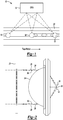
- Direct read after write (DRAW) is often a feature of enterprise level optical tape recording systems. Its purpose is to verify that data has been correctly recorded on optical tape immediately after it has been written. Referring to
Figure 1 , one method for achieving DRAW in anoptical recording system 10 involves using a single optical pickup unit (OPU) 12 with threelaser spots media 20. In this three spot DRAW scheme, while the centralmain spot 16 is used for writing data, one of the twosatellite spots main spot 16, is used to verify data written by themain spot 16 immediately thereafter. - Typical satellite-to-main-spot spacing can be approximately 10 microns. To maintain reasonable OPU component cost, a molded aspheric objective lens is typically employed to form the laser spots at the media surface. Such an asphere has surface profiles that are not portions of a sphere or cylinder. These complex surface profiles can reduce or eliminate spherical aberration and also reduce other optical aberrations, such as distortion, coma, etc., compared to a simple lens. That is, a single aspheric lens can often replace a much more complex multi-lens system. The resulting device is smaller and lighter, and sometimes less costly than multi-lens designs. High numerical aperture single element aspheric lenses, however, have a limited field of view. Hence while the main spot centered on the optical axis has acceptable optical performance, the two satellite spots offset, for example, by approximately 10 microns from the main spot are degraded, meaning they have lower optical performance compared to the main spot.
- One solution to address this limited field of view issue in some optical recording systems is to use multi-element objective lens assemblies. A two-element aspheric objective lens and a single frequency diffraction grating, for example, could be used to generate the three spots at the media plane. A two-element lens assembly, however, is more costly than a single asphere due to the additional cost of the second element along with increased assembly cost from the precise alignment required of the two lens elements. In addition, the extra weight of the two-element objective lens either degrades performance of the focus and tracking actuator or requires a more powerful focus and tracking actuator in order to achieve comparable servo performance. Put a different way, multi-element objective lens assemblies enjoy a wider field of view but with significantly higher cost and weight-both undesirable characteristics in optical recording drive components.
- The reduced field of view in single aspheric lenses-characterized by higher wavefront error, larger spot size, and lower resolution-can degrade the optical system's ability to perform the DRAW function. Certain embodiments described herein attempt to address this issue by compensating for the wavefront error in the satellite spots when using the lower cost, lower weight single aspheric lens. Hence, certain embodiments may enable an optical design to meet functional requirements at lower OPU cost.
- Referring to
Figure 2 , the pair ofsatellite spots frequency diffraction grating 22 in an OPU's optical path preceding anobjective lens 24. The main (central)spot 16 is formed by focusing an un-diffracted (zero order)laser beam 26 through thegrating 22. The satellite spots 14, 18 are created when theobjective lens 24 focuses diffracted (+1 order and -1 order) beams 28, 30 exiting thegrating 22. - In some commercial optical disk drives, the satellite spots 14, 18 are used for purposes other than DRAW. They are used, for example, to generate a special version of the tracking servo error signal known as differential push-pull, and may not require the same optical performance as the
main spot 16. If the satellite spots 14, 18 are instead used for DRAW, they may need to have optical performance (resolution) comparable to that of themain spot 16. Therefore, their wavefront error can be compensated to a level similar to the main (on-axis)spot 16. - Referring to
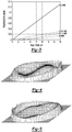
Figure 3 , satellite spots produced at a focal length of 1.765 millimeters by a no cover glass asphere having a numerical aperture of 0.85 and located 10 microns from the main spot would have approximately 0.080 waves of total root mean square (RMS) wavefront error. Hence, the satellite spots would be significantly degraded and have unacceptable resolution for this particular aspheric lens design. Increased satellite spot spacing would further exacerbate total RMS wavefront error in a somewhat linear fashion. - Components of the total RMS wavefront error include spherical aberration (SA) RMS wavefront error, coma aberration (COMA) RMS wavefront error, and astigmatic aberration (ASTIG) RMS wavefront error. Spherical aberration is the only form of monochromatic axial aberration produced by rotationally symmetrical surfaces centered and orthogonal in regard to the optical axis. Spherical aberration will appear whenever optical surface form does not properly match that of the incident wavefront. Thus, it is induced with change of object distance or with multi-surface objectives having deviations in proper spacing. Spherical aberration affects the entire image field, including the very center. Generally, coma aberration occurs either due to the incident wavefront being tilted or decentered with respect to the optical surface. Hence, it is either an aberration affecting off-axis image points or the result of axial misalignment of optical surfaces, respectively. Similar to coma, astigmatic aberration is caused by the inclination of incident wavefronts relative to the optical surface. While coma always originates at the optical surface, astigmatism in its simplest form results from the projectional asymmetry arising from the wavefront's inclination to the surface.
- Referring to
Figures 4 and 5 , +1 order and -1 order diffracted beams have opposite polarity. Because wavefront errors for these beams are inverted, a diffractive optical element could be designed to correct the wavefront error in one satellite spot, but not in both satellite spots simultaneously. Hence, a simple phase or amplitude modulated diffractive optical element designed to correct one satellite spot would cause twice the wavefront error in the other spot. - Holographic optical elements (HOEs) such as volume phase holographic (VPH) transmission gratings work much like conventional surface relief reflection gratings, except in transmission. They are periodic phase structures whose fundamental purpose is to diffract different wavelengths of light from a common input path into different angular output paths. A VPH grating can be formed in a layer of transmissive material, usually dichromated gelatin, which is sealed between two layers of clear glass or fused silica. The phase of incident light is modulated as it passes through the optically thick film that has a periodic differential hardness or refractive index (hence the term "volume phase.") Put a different way, light travelling through a VPH grating undergoes diffraction due to bulk refractive index modulation. This is in contrast to a conventional grating in which the depth of a surface relief pattern modulates the phase of the incident light. As with conventional reflection gratings, the spatial frequency of the periodic structure determines the spectral dispersion or angular separation of wavelength components in the diffracted light. The average refractive index, the refractive index differential or modulation, and the thickness of the film determine the efficiency, polarization, and bandwidth performance characteristics of the grating.
- Because the diffraction mechanism of VPH gratings occurs through the bulk material and without absorption modulation, they give rise to several interesting properties: (1) a theoretical efficiency of 100%, (2) transmission or reflection gratings can be produced depending on the Bragg plane orientation, and (3) undiffracted wavelengths travelling through the grating are not perturbed and can be reused for further purposes. Hence, a HOE can be used to generate satellite spots while at the same time compensating the wavefront error in those spots. The main spot, i.e., the zero order diffractive term, is not affected by the HOE. That is, a VPH grating with its inherent angular selectivity can be created to simultaneously compensate the wavefront error in both satellite spots.
- As mentioned above, VPH gratings can generally be formed in a layer of transmissive material, usually dichromated gelatin, which is sealed between two layers of clear glass or fused silica. More specifically, VPH gratings may be fabricated by the following example method. A photopolymer-based holographic recording film is applied between two glass substrates. The desired diffractive pattern is recorded optically in the film in the form of a phase modulated volume hologram. The desired pattern is recorded by creating an interference between two laser beams, one perfect (collimated and with zero wavefront error) and one containing the inverse of the wavefront error to be corrected. One of the aspheric objective lenses to be corrected could be used in the optical setup for the hologram recording. After "fixing" the diffractive pattern in the recording film layer and applying anti-reflective coatings to the outer surfaces of the substrates, the HOEs are diced into individual elements.
- Referring to
Figure 6 , a setup for recording a volume phase holographic optical element may include alaser diode 32, collimatinglens 34, anddiffraction grating 36. The setup may further includelens pinhole array 42 disposed there between. The setup may also include a high qualitymicroscope objective lens 44 and asphericobjective lens 46. The aspheric objective lens directs optical beams ontoholographic recording film 48. All optical components, other than the asphericobjective lens 46, may be designed or selected to have very high optical performance, i.e., low wavefront error, so that theholographic recording file 48 records only the wavefront variation introduced by the asphericobjective lens 46 and not errors attributed to other components in the setup. - Referring to
Figure 7 , another setup for recording a volume phase holographic optical element may include alaser diode 50, collimatinglens 52, andpolarizing beam splitter 54. Thepolarizing beam splitter 54 creates two separate optical paths. The first optical path may include aretarder 56, grating 58, andlens reflective pinhole array 64 disposed there between. The first optical path may further includemirror 66,objective lens 68, and asphericobjective lens 70. The second optical path may includemirror 72,lens 74,pinhole 76,lens 78, andretarder 80. Finally, the setup may include anamplitude beam splitter 82. The separate optical paths created by thepolarizing beam splitter 54 are combined by theamplitude beam splitter 82 and directed ontoholographic film 84. - In this setup, the zero order (un-diffracted) beam from the
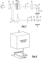
lens 60 is reflected by the mirroredpinhole array 64 while the +1 order and -1 order diffracted beams pass through it. Thepolarizing beam splitter 54 and quarter wave plate (λ/4 retarder) 56 act as an optical isolator, reflecting the zero order beam along a separate optical path. As mentioned above, the beams recombine at theamplitude beam splitter 82 and then interfere at theholographic recording film 84. The half wave (λ/2)plate retarder 80 rotates the polarization to match that of the +1 order and -1 order beams so they will interfere properly at the film plane. Hence, the zero order beam can be made to have nearly zero wavefront error before re-combining with the other two beams. Other setups are of course also possible. - The setups described herein can be arranged with other equipment to form high volume recording systems to efficiently create large numbers of holograms. Referring to
Figure 8 for example, aholographic recording plate 86, perhaps up to 12 inches by 12 inches, may be mounted on an automated X,Y stage 88 for step-and-repeat recording of holograms via hologram recorderoptical system 90. As an example, more than 3,500 5 millimeter by 5 millimeter holograms could be recorded on the 12 inchsquare plate 86. After recording and fixing the patterns, individual holograms can be diced up in a fashion similar to integrated circuits or other wafer-scale optical components for use in optical tape pick up units. - Referring to
Figure 9 , anoptical tape system 92 includes, inter alia, at least oneOPU 94. TheOPU 94 includes alaser 96, other OPU elements 98 (as is common),HOE 100, and asphericobjective lens 102. The optical path through these elements is depicted by heavy line. TheHOE 100 pre-compensates wavefront error of the +1 order and -1 order diffracted beams before entering the asphericobjective lens 102. That is, theHOE 100 introduces wavefront error into the +1 order beam that is of a magnitude approximately equal to and a polarity opposite that of the wavefront error introduced into the +1 order beam by the asphericobjective lens 102, and introduces wavefront error into the -1 order beam that is of a magnitude approximately equal to and a polarity opposite that of the wavefront error introduced into the -1 order beam by the asphericobjective lens 102. Hence, the wavefront error of the +1 order and -1 order diffracted beams exiting the asphericobjective lens 102 can be, for example, 50 milliwaves or less. - While exemplary embodiments are described above, it is not intended that these embodiments describe all possible forms encompassed by the claims. The words used in the specification are words of description rather than limitation, and it is understood that various changes may be made without departing from scope of the invention, which is defined by the appended claims. As previously described, the features of various embodiments can be combined to form further embodiments of the invention that may not be explicitly described or illustrated. While various embodiments could have been described as providing advantages or being preferred over other embodiments or prior art implementations with respect to one or more desired characteristics, those of ordinary skill in the art recognize that one or more features or characteristics can be compromised to achieve desired overall system attributes, which depend on the specific application and implementation. These attributes may include, but are not limited to cost, strength, durability, life cycle cost, marketability, appearance, packaging, size, serviceability, weight, manufacturability, ease of assembly, etc. As such, embodiments described as less desirable than other embodiments or prior art implementations with respect to one or more characteristics are not outside the scope of the disclosure and can be desirable for particular applications.
Claims (7)
- An optical tape pick up system (92) configured to perform direct read after write, DRAW, by using three laser spots comprising a main central spot (16) and two satellite spots (14, 18), wherein the main central spot is used for writing onto optical tape (20) and one of the satellite spots is used for verify data written by the main central spot immediately thereafter, the optical tape system comprising:a holographic optical element (100) configured to split a laser beam into a zero order and +1 and -1 first order beams and to introduce wavefront error via diffaction into the first order beams but not the zero order beam; andan aspheric objective lens (102) configured to focus the beams onto optical tape and to introduce wavefront error into the first order beams;wherein the wavefront error introduced by the holographic optical element (100) has a specified polarity and magnitude to offset the wavefront error introduced by the aspheric objective lens (102) so as to reduce the resulting wavefront error of the focused first order beams.
- The system of claim 1, wherein the resulting wavefront error has a value less than 50 milliwaves.
- The system of claim 2, wherein the resulting wavefront error has a value less than 40 milliwaves.
- The system of any preceding claim, wherein the wavefront error introduced into the +1 order beam by the aspheric objective lens has a polarity opposite, and a magnitude approximately equal, to that of the wavefront error introduced into the +1 order beam by the holographic optical element, and wherein the wavefront error introduced into the -1 order beam by the aspheric objective lens has a polarity opposite, and a magnitude approximately equal, to that of the wavefront error introduced into the -1 order beam by the holographic optical element.
- The system of any preceding claim, wherein the aspheric objective lens is a no cover glass aspheric objective lens.
- The system of any preceding claim, wherein the aspheric objective lens has only a single glass element.
- The system of any preceding claim, wherein the holographic optical element is a volume phase holographic grating.
Applications Claiming Priority (2)
| Application Number | Priority Date | Filing Date | Title |
|---|---|---|---|
| US13/682,915 US9245572B2 (en) | 2012-11-21 | 2012-11-21 | Optical tape pick up unit with holographic optical element |
| PCT/US2013/063973 WO2014081513A1 (en) | 2012-11-21 | 2013-10-09 | Optical tape pick up unit with holographic optical element |
Publications (2)
| Publication Number | Publication Date |
|---|---|
| EP2923356A1 EP2923356A1 (en) | 2015-09-30 |
| EP2923356B1 true EP2923356B1 (en) | 2019-05-01 |
Family
ID=49382668
Family Applications (1)
| Application Number | Title | Priority Date | Filing Date |
|---|---|---|---|
| EP13777463.4A Active EP2923356B1 (en) | 2012-11-21 | 2013-10-09 | Optical tape pick up unit with holographic optical element |
Country Status (7)
| Country | Link |
|---|---|
| US (1) | US9245572B2 (en) |
| EP (1) | EP2923356B1 (en) |
| JP (1) | JP6234470B2 (en) |
| CN (1) | CN104813397B (en) |
| AU (1) | AU2013348369B2 (en) |
| NZ (1) | NZ707231A (en) |
| WO (1) | WO2014081513A1 (en) |
Cited By (1)
| Publication number | Priority date | Publication date | Assignee | Title |
|---|---|---|---|---|
| WO2022207784A1 (en) * | 2021-04-01 | 2022-10-06 | Metamaterial Technologies Canada Inc. | Wafer-level optics assembly with holographic optical element |
Family Cites Families (23)
| Publication number | Priority date | Publication date | Assignee | Title |
|---|---|---|---|---|
| NL8800057A (en) * | 1988-01-11 | 1989-08-01 | Philips Nv | OPTICAL SCANNER. |
| NL8800133A (en) * | 1988-01-21 | 1989-08-16 | Philips Nv | DEVICE FOR SCANNING AN INFORMATION SHEET WITH OPTICAL RADIATION. |
| US5490133A (en) * | 1990-10-05 | 1996-02-06 | Hitachi, Ltd. | Optical information processing apparatus and method of controlling position of optical spot and reproducing signals |
| US5272690A (en) * | 1992-03-05 | 1993-12-21 | International Business Machines Corporation | Hologram element system |
| US5835471A (en) | 1995-06-12 | 1998-11-10 | Canon Kabushiki Kaisha | Optical information recording and/or reproducing apparatus |
| JP2000099980A (en) | 1998-09-17 | 2000-04-07 | Toshiba Corp | Optical device used for optical disk recording/ reproducing device |
| JP2000293883A (en) * | 1999-04-08 | 2000-10-20 | Ricoh Co Ltd | Optical pickup |
| KR100694032B1 (en) * | 2000-04-17 | 2007-03-12 | 삼성전자주식회사 | Objective lens and the optical pickup device adopting the same |
| JP2002163830A (en) * | 2000-11-24 | 2002-06-07 | Toshiba Corp | Optical information processing system by making use of optical aberration and information medium having recording layer which is protected by transparent layer with uneven thickness |
| AU2002348880A1 (en) * | 2001-12-07 | 2003-06-17 | Koninklijke Philips Electronics N.V. | Field curvature reduction for optical system |
| CN1466133A (en) * | 2002-07-01 | 2004-01-07 | 汕头高新区和川光电科技有限公司 | Optical read/write device |
| KR100911141B1 (en) * | 2002-09-03 | 2009-08-06 | 삼성전자주식회사 | Lens capable of compensating wavefront error induced by tilt and optical pickup |
| EP1489604A1 (en) | 2003-06-19 | 2004-12-22 | Deutsche Thomson-Brandt Gmbh | Method for detecting spherical aberration |
| JP2006012218A (en) * | 2004-06-22 | 2006-01-12 | Konica Minolta Opto Inc | Condensing optical element and optical pickup device |
| JP4925256B2 (en) * | 2006-01-20 | 2012-04-25 | 株式会社リコー | Light source unit, light detection unit, optical pickup device, and optical disk device |
| WO2007092785A2 (en) | 2006-02-02 | 2007-08-16 | Otsi Holdings Llc | Optical tape media, marking, systems, and apparatus and process for producing thereof |
| JP4797706B2 (en) * | 2006-03-03 | 2011-10-19 | 旭硝子株式会社 | Optical head device |
| KR20080110999A (en) * | 2006-03-07 | 2008-12-22 | 코니카 미놀타 옵토 인코포레이티드 | Optical pickup apparatus, objective optical element, and optical information recording and reproducing apparatus |
| US7920339B2 (en) * | 2008-07-02 | 2011-04-05 | Aptina Imaging Corporation | Method and apparatus providing singlet wafer lens system with field flattener |
| US8451702B2 (en) | 2011-08-22 | 2013-05-28 | Oracle International Corporation | Direct read after write for optical storage device |
| JP6032634B2 (en) * | 2011-09-22 | 2016-11-30 | パナソニックIpマネジメント株式会社 | Optical pickup and optical recording / reproducing apparatus |
| JP2013084329A (en) * | 2011-09-29 | 2013-05-09 | Panasonic Corp | Optical pickup device and optical reproduction device |
| US8792317B2 (en) | 2012-03-09 | 2014-07-29 | Oracle International Corporation | Optical storage device with direct read after write |
-
2012
- 2012-11-21 US US13/682,915 patent/US9245572B2/en active Active
-
2013
- 2013-10-09 JP JP2015544067A patent/JP6234470B2/en active Active
- 2013-10-09 CN CN201380060510.1A patent/CN104813397B/en active Active
- 2013-10-09 EP EP13777463.4A patent/EP2923356B1/en active Active
- 2013-10-09 NZ NZ707231A patent/NZ707231A/en unknown
- 2013-10-09 AU AU2013348369A patent/AU2013348369B2/en active Active
- 2013-10-09 WO PCT/US2013/063973 patent/WO2014081513A1/en active Application Filing
Non-Patent Citations (1)
| Title |
|---|
| None * |
Cited By (1)
| Publication number | Priority date | Publication date | Assignee | Title |
|---|---|---|---|---|
| WO2022207784A1 (en) * | 2021-04-01 | 2022-10-06 | Metamaterial Technologies Canada Inc. | Wafer-level optics assembly with holographic optical element |
Also Published As
| Publication number | Publication date |
|---|---|
| EP2923356A1 (en) | 2015-09-30 |
| US9245572B2 (en) | 2016-01-26 |
| NZ707231A (en) | 2017-01-27 |
| WO2014081513A1 (en) | 2014-05-30 |
| JP6234470B2 (en) | 2017-11-22 |
| AU2013348369A1 (en) | 2015-05-14 |
| CN104813397A (en) | 2015-07-29 |
| JP2016502222A (en) | 2016-01-21 |
| CN104813397B (en) | 2018-07-17 |
| AU2013348369B2 (en) | 2017-09-28 |
| US20140140184A1 (en) | 2014-05-22 |
Similar Documents
| Publication | Publication Date | Title |
|---|---|---|
| KR100653289B1 (en) | Optical head and recording/reproducing device | |
| US7385906B2 (en) | Objective lens, optical pickup, and optical information processing apparatus using the same | |
| EP1202259A2 (en) | Objective lens, light converging optical system, optical pickup apparatus, and recording/reproducing apparatus | |
| US6618343B1 (en) | Optical information processor and optical element | |
| US7233562B2 (en) | Optical pickup device | |
| EP2923356B1 (en) | Optical tape pick up unit with holographic optical element | |
| US8085626B2 (en) | Optical pickup device and lens for optical pickup | |
| KR100782813B1 (en) | Active compensation device and compatible optical pickup and optical recording and/or reproducing apparatus employing the same | |
| JP3297505B2 (en) | Optical head device and optical information device | |
| US8531926B2 (en) | Optical system for optical pickup | |
| US7038978B2 (en) | Optical information recording and reproducing apparatus for recording information bits into an optical disk in a three dimensional arrangement | |
| KR101120026B1 (en) | Active compensation device and compatible optical pickup and optical recording and/or reproducing apparatus employing it | |
| JP4596938B2 (en) | Optical pickup, optical information processing device | |
| US7671312B2 (en) | Optical pickup system, optical system, and optical information recording medium | |
| US20060098287A1 (en) | Diffractive optical element and optical pickup device using the same | |
| JP4768676B2 (en) | Optical pickup and optical information processing apparatus | |
| JP2006209821A (en) | Optical pickup and optical information processing system using it | |
| CN101248488A (en) | A compatible optical pickup and an optical recording and/or reproducing apparatus employing a compatible optical pickup | |
| JP2002040324A (en) | Optical device for compensating chromatic aberration and optical pickup device |
Legal Events
| Date | Code | Title | Description |
|---|---|---|---|
| PUAI | Public reference made under article 153(3) epc to a published international application that has entered the european phase |
Free format text: ORIGINAL CODE: 0009012 |
|
| 17P | Request for examination filed |
Effective date: 20150622 |
|
| AK | Designated contracting states |
Kind code of ref document: A1 Designated state(s): AL AT BE BG CH CY CZ DE DK EE ES FI FR GB GR HR HU IE IS IT LI LT LU LV MC MK MT NL NO PL PT RO RS SE SI SK SM TR |
|
| AX | Request for extension of the european patent |
Extension state: BA ME |
|
| DAX | Request for extension of the european patent (deleted) | ||
| GRAP | Despatch of communication of intention to grant a patent |
Free format text: ORIGINAL CODE: EPIDOSNIGR1 |
|
| STAA | Information on the status of an ep patent application or granted ep patent |
Free format text: STATUS: GRANT OF PATENT IS INTENDED |
|
| INTG | Intention to grant announced |
Effective date: 20181120 |
|
| GRAS | Grant fee paid |
Free format text: ORIGINAL CODE: EPIDOSNIGR3 |
|
| GRAA | (expected) grant |
Free format text: ORIGINAL CODE: 0009210 |
|
| STAA | Information on the status of an ep patent application or granted ep patent |
Free format text: STATUS: THE PATENT HAS BEEN GRANTED |
|
| AK | Designated contracting states |
Kind code of ref document: B1 Designated state(s): AL AT BE BG CH CY CZ DE DK EE ES FI FR GB GR HR HU IE IS IT LI LT LU LV MC MK MT NL NO PL PT RO RS SE SI SK SM TR |
|
| REG | Reference to a national code |
Ref country code: GB Ref legal event code: FG4D |
|
| REG | Reference to a national code |
Ref country code: CH Ref legal event code: EP Ref country code: AT Ref legal event code: REF Ref document number: 1127992 Country of ref document: AT Kind code of ref document: T Effective date: 20190515 |
|
| REG | Reference to a national code |
Ref country code: DE Ref legal event code: R096 Ref document number: 602013054695 Country of ref document: DE |
|
| REG | Reference to a national code |
Ref country code: IE Ref legal event code: FG4D |
|
| REG | Reference to a national code |
Ref country code: NL Ref legal event code: MP Effective date: 20190501 |
|
| REG | Reference to a national code |
Ref country code: LT Ref legal event code: MG4D |
|
| PG25 | Lapsed in a contracting state [announced via postgrant information from national office to epo] |
Ref country code: HR Free format text: LAPSE BECAUSE OF FAILURE TO SUBMIT A TRANSLATION OF THE DESCRIPTION OR TO PAY THE FEE WITHIN THE PRESCRIBED TIME-LIMIT Effective date: 20190501 Ref country code: NO Free format text: LAPSE BECAUSE OF FAILURE TO SUBMIT A TRANSLATION OF THE DESCRIPTION OR TO PAY THE FEE WITHIN THE PRESCRIBED TIME-LIMIT Effective date: 20190801 Ref country code: NL Free format text: LAPSE BECAUSE OF FAILURE TO SUBMIT A TRANSLATION OF THE DESCRIPTION OR TO PAY THE FEE WITHIN THE PRESCRIBED TIME-LIMIT Effective date: 20190501 Ref country code: ES Free format text: LAPSE BECAUSE OF FAILURE TO SUBMIT A TRANSLATION OF THE DESCRIPTION OR TO PAY THE FEE WITHIN THE PRESCRIBED TIME-LIMIT Effective date: 20190501 Ref country code: LT Free format text: LAPSE BECAUSE OF FAILURE TO SUBMIT A TRANSLATION OF THE DESCRIPTION OR TO PAY THE FEE WITHIN THE PRESCRIBED TIME-LIMIT Effective date: 20190501 Ref country code: AL Free format text: LAPSE BECAUSE OF FAILURE TO SUBMIT A TRANSLATION OF THE DESCRIPTION OR TO PAY THE FEE WITHIN THE PRESCRIBED TIME-LIMIT Effective date: 20190501 Ref country code: PT Free format text: LAPSE BECAUSE OF FAILURE TO SUBMIT A TRANSLATION OF THE DESCRIPTION OR TO PAY THE FEE WITHIN THE PRESCRIBED TIME-LIMIT Effective date: 20190901 Ref country code: SE Free format text: LAPSE BECAUSE OF FAILURE TO SUBMIT A TRANSLATION OF THE DESCRIPTION OR TO PAY THE FEE WITHIN THE PRESCRIBED TIME-LIMIT Effective date: 20190501 Ref country code: FI Free format text: LAPSE BECAUSE OF FAILURE TO SUBMIT A TRANSLATION OF THE DESCRIPTION OR TO PAY THE FEE WITHIN THE PRESCRIBED TIME-LIMIT Effective date: 20190501 |
|
| PG25 | Lapsed in a contracting state [announced via postgrant information from national office to epo] |
Ref country code: BG Free format text: LAPSE BECAUSE OF FAILURE TO SUBMIT A TRANSLATION OF THE DESCRIPTION OR TO PAY THE FEE WITHIN THE PRESCRIBED TIME-LIMIT Effective date: 20190801 Ref country code: GR Free format text: LAPSE BECAUSE OF FAILURE TO SUBMIT A TRANSLATION OF THE DESCRIPTION OR TO PAY THE FEE WITHIN THE PRESCRIBED TIME-LIMIT Effective date: 20190802 Ref country code: LV Free format text: LAPSE BECAUSE OF FAILURE TO SUBMIT A TRANSLATION OF THE DESCRIPTION OR TO PAY THE FEE WITHIN THE PRESCRIBED TIME-LIMIT Effective date: 20190501 Ref country code: RS Free format text: LAPSE BECAUSE OF FAILURE TO SUBMIT A TRANSLATION OF THE DESCRIPTION OR TO PAY THE FEE WITHIN THE PRESCRIBED TIME-LIMIT Effective date: 20190501 |
|
| REG | Reference to a national code |
Ref country code: AT Ref legal event code: MK05 Ref document number: 1127992 Country of ref document: AT Kind code of ref document: T Effective date: 20190501 |
|
| PG25 | Lapsed in a contracting state [announced via postgrant information from national office to epo] |
Ref country code: IS Free format text: LAPSE BECAUSE OF FAILURE TO SUBMIT A TRANSLATION OF THE DESCRIPTION OR TO PAY THE FEE WITHIN THE PRESCRIBED TIME-LIMIT Effective date: 20190901 |
|
| PG25 | Lapsed in a contracting state [announced via postgrant information from national office to epo] |
Ref country code: SK Free format text: LAPSE BECAUSE OF FAILURE TO SUBMIT A TRANSLATION OF THE DESCRIPTION OR TO PAY THE FEE WITHIN THE PRESCRIBED TIME-LIMIT Effective date: 20190501 Ref country code: RO Free format text: LAPSE BECAUSE OF FAILURE TO SUBMIT A TRANSLATION OF THE DESCRIPTION OR TO PAY THE FEE WITHIN THE PRESCRIBED TIME-LIMIT Effective date: 20190501 Ref country code: CZ Free format text: LAPSE BECAUSE OF FAILURE TO SUBMIT A TRANSLATION OF THE DESCRIPTION OR TO PAY THE FEE WITHIN THE PRESCRIBED TIME-LIMIT Effective date: 20190501 Ref country code: DK Free format text: LAPSE BECAUSE OF FAILURE TO SUBMIT A TRANSLATION OF THE DESCRIPTION OR TO PAY THE FEE WITHIN THE PRESCRIBED TIME-LIMIT Effective date: 20190501 Ref country code: AT Free format text: LAPSE BECAUSE OF FAILURE TO SUBMIT A TRANSLATION OF THE DESCRIPTION OR TO PAY THE FEE WITHIN THE PRESCRIBED TIME-LIMIT Effective date: 20190501 Ref country code: EE Free format text: LAPSE BECAUSE OF FAILURE TO SUBMIT A TRANSLATION OF THE DESCRIPTION OR TO PAY THE FEE WITHIN THE PRESCRIBED TIME-LIMIT Effective date: 20190501 |
|
| REG | Reference to a national code |
Ref country code: DE Ref legal event code: R097 Ref document number: 602013054695 Country of ref document: DE |
|
| PG25 | Lapsed in a contracting state [announced via postgrant information from national office to epo] |
Ref country code: SM Free format text: LAPSE BECAUSE OF FAILURE TO SUBMIT A TRANSLATION OF THE DESCRIPTION OR TO PAY THE FEE WITHIN THE PRESCRIBED TIME-LIMIT Effective date: 20190501 Ref country code: IT Free format text: LAPSE BECAUSE OF FAILURE TO SUBMIT A TRANSLATION OF THE DESCRIPTION OR TO PAY THE FEE WITHIN THE PRESCRIBED TIME-LIMIT Effective date: 20190501 |
|
| PLBE | No opposition filed within time limit |
Free format text: ORIGINAL CODE: 0009261 |
|
| STAA | Information on the status of an ep patent application or granted ep patent |
Free format text: STATUS: NO OPPOSITION FILED WITHIN TIME LIMIT |
|
| PG25 | Lapsed in a contracting state [announced via postgrant information from national office to epo] |
Ref country code: TR Free format text: LAPSE BECAUSE OF FAILURE TO SUBMIT A TRANSLATION OF THE DESCRIPTION OR TO PAY THE FEE WITHIN THE PRESCRIBED TIME-LIMIT Effective date: 20190501 |
|
| 26N | No opposition filed |
Effective date: 20200204 |
|
| PG25 | Lapsed in a contracting state [announced via postgrant information from national office to epo] |
Ref country code: PL Free format text: LAPSE BECAUSE OF FAILURE TO SUBMIT A TRANSLATION OF THE DESCRIPTION OR TO PAY THE FEE WITHIN THE PRESCRIBED TIME-LIMIT Effective date: 20190501 |
|
| PG25 | Lapsed in a contracting state [announced via postgrant information from national office to epo] |
Ref country code: MC Free format text: LAPSE BECAUSE OF FAILURE TO SUBMIT A TRANSLATION OF THE DESCRIPTION OR TO PAY THE FEE WITHIN THE PRESCRIBED TIME-LIMIT Effective date: 20190501 Ref country code: SI Free format text: LAPSE BECAUSE OF FAILURE TO SUBMIT A TRANSLATION OF THE DESCRIPTION OR TO PAY THE FEE WITHIN THE PRESCRIBED TIME-LIMIT Effective date: 20190501 |
|
| REG | Reference to a national code |
Ref country code: CH Ref legal event code: PL |
|
| PG25 | Lapsed in a contracting state [announced via postgrant information from national office to epo] |
Ref country code: LU Free format text: LAPSE BECAUSE OF NON-PAYMENT OF DUE FEES Effective date: 20191009 Ref country code: LI Free format text: LAPSE BECAUSE OF NON-PAYMENT OF DUE FEES Effective date: 20191031 Ref country code: CH Free format text: LAPSE BECAUSE OF NON-PAYMENT OF DUE FEES Effective date: 20191031 |
|
| REG | Reference to a national code |
Ref country code: BE Ref legal event code: MM Effective date: 20191031 |
|
| PG25 | Lapsed in a contracting state [announced via postgrant information from national office to epo] |
Ref country code: BE Free format text: LAPSE BECAUSE OF NON-PAYMENT OF DUE FEES Effective date: 20191031 |
|
| PG25 | Lapsed in a contracting state [announced via postgrant information from national office to epo] |
Ref country code: IE Free format text: LAPSE BECAUSE OF NON-PAYMENT OF DUE FEES Effective date: 20191009 Ref country code: FR Free format text: LAPSE BECAUSE OF NON-PAYMENT OF DUE FEES Effective date: 20191031 |
|
| PG25 | Lapsed in a contracting state [announced via postgrant information from national office to epo] |
Ref country code: CY Free format text: LAPSE BECAUSE OF FAILURE TO SUBMIT A TRANSLATION OF THE DESCRIPTION OR TO PAY THE FEE WITHIN THE PRESCRIBED TIME-LIMIT Effective date: 20190501 |
|
| PG25 | Lapsed in a contracting state [announced via postgrant information from national office to epo] |
Ref country code: HU Free format text: LAPSE BECAUSE OF FAILURE TO SUBMIT A TRANSLATION OF THE DESCRIPTION OR TO PAY THE FEE WITHIN THE PRESCRIBED TIME-LIMIT; INVALID AB INITIO Effective date: 20131009 Ref country code: MT Free format text: LAPSE BECAUSE OF FAILURE TO SUBMIT A TRANSLATION OF THE DESCRIPTION OR TO PAY THE FEE WITHIN THE PRESCRIBED TIME-LIMIT Effective date: 20190501 |
|
| PG25 | Lapsed in a contracting state [announced via postgrant information from national office to epo] |
Ref country code: MK Free format text: LAPSE BECAUSE OF FAILURE TO SUBMIT A TRANSLATION OF THE DESCRIPTION OR TO PAY THE FEE WITHIN THE PRESCRIBED TIME-LIMIT Effective date: 20190501 |
|
| P01 | Opt-out of the competence of the unified patent court (upc) registered |
Effective date: 20230522 |
|
| PGFP | Annual fee paid to national office [announced via postgrant information from national office to epo] |
Ref country code: GB Payment date: 20230831 Year of fee payment: 11 |
|
| PGFP | Annual fee paid to national office [announced via postgrant information from national office to epo] |
Ref country code: DE Payment date: 20230830 Year of fee payment: 11 |