EP2922092A1 - Semiconductor device - Google Patents
Semiconductor device Download PDFInfo
- Publication number
- EP2922092A1 EP2922092A1 EP13851700.8A EP13851700A EP2922092A1 EP 2922092 A1 EP2922092 A1 EP 2922092A1 EP 13851700 A EP13851700 A EP 13851700A EP 2922092 A1 EP2922092 A1 EP 2922092A1
- Authority
- EP
- European Patent Office
- Prior art keywords
- shield plate
- semiconductor device
- support
- outer case
- convex portion
- Prior art date
- Legal status (The legal status is an assumption and is not a legal conclusion. Google has not performed a legal analysis and makes no representation as to the accuracy of the status listed.)
- Granted
Links
Images





Classifications
-
- H—ELECTRICITY
- H10—SEMICONDUCTOR DEVICES; ELECTRIC SOLID-STATE DEVICES NOT OTHERWISE PROVIDED FOR
- H10W—GENERIC PACKAGES, INTERCONNECTIONS, CONNECTORS OR OTHER CONSTRUCTIONAL DETAILS OF DEVICES COVERED BY CLASS H10
- H10W42/00—Arrangements for protection of devices
- H10W42/20—Arrangements for protection of devices protecting against electromagnetic or particle radiation, e.g. light, X-rays, gamma-rays or electrons
-
- H—ELECTRICITY
- H05—ELECTRIC TECHNIQUES NOT OTHERWISE PROVIDED FOR
- H05K—PRINTED CIRCUITS; CASINGS OR CONSTRUCTIONAL DETAILS OF ELECTRIC APPARATUS; MANUFACTURE OF ASSEMBLAGES OF ELECTRICAL COMPONENTS
- H05K7/00—Constructional details common to different types of electric apparatus
- H05K7/14—Mounting supporting structure in casing or on frame or rack
- H05K7/1422—Printed circuit boards receptacles, e.g. stacked structures, electronic circuit modules or box like frames
- H05K7/1427—Housings
-
- H—ELECTRICITY
- H05—ELECTRIC TECHNIQUES NOT OTHERWISE PROVIDED FOR
- H05K—PRINTED CIRCUITS; CASINGS OR CONSTRUCTIONAL DETAILS OF ELECTRIC APPARATUS; MANUFACTURE OF ASSEMBLAGES OF ELECTRICAL COMPONENTS
- H05K7/00—Constructional details common to different types of electric apparatus
- H05K7/14—Mounting supporting structure in casing or on frame or rack
- H05K7/1422—Printed circuit boards receptacles, e.g. stacked structures, electronic circuit modules or box like frames
- H05K7/1427—Housings
- H05K7/1432—Housings specially adapted for power drive units or power converters
- H05K7/14322—Housings specially adapted for power drive units or power converters wherein the control and power circuits of a power converter are arranged within the same casing
-
- H—ELECTRICITY
- H05—ELECTRIC TECHNIQUES NOT OTHERWISE PROVIDED FOR
- H05K—PRINTED CIRCUITS; CASINGS OR CONSTRUCTIONAL DETAILS OF ELECTRIC APPARATUS; MANUFACTURE OF ASSEMBLAGES OF ELECTRICAL COMPONENTS
- H05K9/00—Screening of apparatus or components against electric or magnetic fields
- H05K9/0007—Casings
- H05K9/002—Casings with localised screening
- H05K9/0022—Casings with localised screening of components mounted on printed circuit boards [PCB]
-
- H—ELECTRICITY
- H05—ELECTRIC TECHNIQUES NOT OTHERWISE PROVIDED FOR
- H05K—PRINTED CIRCUITS; CASINGS OR CONSTRUCTIONAL DETAILS OF ELECTRIC APPARATUS; MANUFACTURE OF ASSEMBLAGES OF ELECTRICAL COMPONENTS
- H05K9/00—Screening of apparatus or components against electric or magnetic fields
- H05K9/0007—Casings
- H05K9/002—Casings with localised screening
- H05K9/0022—Casings with localised screening of components mounted on printed circuit boards [PCB]
- H05K9/0037—Housings with compartments containing a PCB, e.g. partitioning walls
-
- H—ELECTRICITY
- H10—SEMICONDUCTOR DEVICES; ELECTRIC SOLID-STATE DEVICES NOT OTHERWISE PROVIDED FOR
- H10W—GENERIC PACKAGES, INTERCONNECTIONS, CONNECTORS OR OTHER CONSTRUCTIONAL DETAILS OF DEVICES COVERED BY CLASS H10
- H10W90/00—Package configurations
-
- H—ELECTRICITY
- H02—GENERATION; CONVERSION OR DISTRIBUTION OF ELECTRIC POWER
- H02M—APPARATUS FOR CONVERSION BETWEEN AC AND AC, BETWEEN AC AND DC, OR BETWEEN DC AND DC, AND FOR USE WITH MAINS OR SIMILAR POWER SUPPLY SYSTEMS; CONVERSION OF DC OR AC INPUT POWER INTO SURGE OUTPUT POWER; CONTROL OR REGULATION THEREOF
- H02M7/00—Conversion of AC power input into DC power output; Conversion of DC power input into AC power output
- H02M7/003—Constructional details, e.g. physical layout, assembly, wiring or busbar connections
-
- H—ELECTRICITY
- H10—SEMICONDUCTOR DEVICES; ELECTRIC SOLID-STATE DEVICES NOT OTHERWISE PROVIDED FOR
- H10W—GENERIC PACKAGES, INTERCONNECTIONS, CONNECTORS OR OTHER CONSTRUCTIONAL DETAILS OF DEVICES COVERED BY CLASS H10
- H10W72/00—Interconnections or connectors in packages
- H10W72/50—Bond wires
- H10W72/531—Shapes of wire connectors
- H10W72/5363—Shapes of wire connectors the connected ends being wedge-shaped
-
- H—ELECTRICITY
- H10—SEMICONDUCTOR DEVICES; ELECTRIC SOLID-STATE DEVICES NOT OTHERWISE PROVIDED FOR
- H10W—GENERIC PACKAGES, INTERCONNECTIONS, CONNECTORS OR OTHER CONSTRUCTIONAL DETAILS OF DEVICES COVERED BY CLASS H10
- H10W72/00—Interconnections or connectors in packages
- H10W72/50—Bond wires
- H10W72/541—Dispositions of bond wires
- H10W72/5438—Dispositions of bond wires the bond wires having multiple connections on the same bond pad
-
- H—ELECTRICITY
- H10—SEMICONDUCTOR DEVICES; ELECTRIC SOLID-STATE DEVICES NOT OTHERWISE PROVIDED FOR
- H10W—GENERIC PACKAGES, INTERCONNECTIONS, CONNECTORS OR OTHER CONSTRUCTIONAL DETAILS OF DEVICES COVERED BY CLASS H10
- H10W74/00—Encapsulations, e.g. protective coatings
-
- H—ELECTRICITY
- H10—SEMICONDUCTOR DEVICES; ELECTRIC SOLID-STATE DEVICES NOT OTHERWISE PROVIDED FOR
- H10W—GENERIC PACKAGES, INTERCONNECTIONS, CONNECTORS OR OTHER CONSTRUCTIONAL DETAILS OF DEVICES COVERED BY CLASS H10
- H10W90/00—Package configurations
- H10W90/701—Package configurations characterised by the relative positions of pads or connectors relative to package parts
- H10W90/751—Package configurations characterised by the relative positions of pads or connectors relative to package parts of bond wires
- H10W90/753—Package configurations characterised by the relative positions of pads or connectors relative to package parts of bond wires between laterally-adjacent chips
-
- H—ELECTRICITY
- H10—SEMICONDUCTOR DEVICES; ELECTRIC SOLID-STATE DEVICES NOT OTHERWISE PROVIDED FOR
- H10W—GENERIC PACKAGES, INTERCONNECTIONS, CONNECTORS OR OTHER CONSTRUCTIONAL DETAILS OF DEVICES COVERED BY CLASS H10
- H10W90/00—Package configurations
- H10W90/701—Package configurations characterised by the relative positions of pads or connectors relative to package parts
- H10W90/751—Package configurations characterised by the relative positions of pads or connectors relative to package parts of bond wires
- H10W90/754—Package configurations characterised by the relative positions of pads or connectors relative to package parts of bond wires between a chip and a stacked insulating package substrate, interposer or RDL
Definitions
- the present invention relates to a semiconductor device, and more particularly, to a semiconductor device in which a control circuit board is fixed to an outer case that accommodates a power semiconductor element.
- a semiconductor module in which a power semiconductor element such as an insulated gate bipolar transistor (IGBT) is built into an outer case made from a resin is known as an example of a semiconductor device that controls a motor or the like.
- a semiconductor module including a control circuit board that controls a power semiconductor element is also known.
- noise generated during a switching operation of a power semiconductor element may have an influence on the control circuit board and the power semiconductor element.
- the control circuit board is fixed to the outer case to be separated from the power semiconductor element such that the influence of noise does not reach.
- the control circuit board is fixed to an outer side of the outer case by screw-clamping, for example.
- Patent Literature 1 a semiconductor device in which the shield plate is fixed by screw-clamping is known.
- Patent Literature 2 a semiconductor device in which a print board having a shield layer is fixed by screw-clamping to external connection terminals fixed and supported on an outer case.
- Patent Literature 3 a semiconductor device in which a shield plate is mounted on the ends of step supports implanted in an outer case, a metal ring is placed so that a coupling portion of each of the step supports passes through the metal ring, a control circuit board is mounted on the metal rings, the control circuit board and the shield plate overlapped in two stages are fixed by screw-clamping to the step supports.
- these semiconductor devices have the shield plate arranged between the power semiconductor element and the control circuit board, it is possible to suppress noise radiating from one of the power semiconductor element and the control circuit board from entering into the other by being partially blocked by the shield plate.
- a metal plate made from a material corresponding the properties of noise is used as the shield plate, and it is possible to effectively block noise.
- Patent Literature 1 to 3 use metal screws or metal rings in order to fix the shield plate.
- metal components since metal components are used, it is necessary to design by taking a separation distance between the shield plate and the control circuit board mounted above the shield plate into consideration and to prepare a void distance corresponding to a screw height between the shield plate and the control circuit board. Therefore, the overall height of the semiconductor device having the control circuit board increases and the volume increases.
- the present invention solves the above problems advantageously, and an object thereof is to provide a semiconductor device having a control circuit board, capable of fixing a shield plate without using screws and reducing the thickness and the size.
- the semiconductor device includes: a semiconductor element accommodated in an outer case; a control circuit board fixed to the outer case to be separated from the semiconductor element; and a shield plate provided between the semiconductor element and the control circuit board.
- the outer case is provided with a support having a convex portion longer than a thickness of the shield plate at a distal end thereof. A through-hole through which the convex portion of the support passes is formed in the shield plate.
- the shield plate is fixed to the support by fixing means that engages with the convex portion.
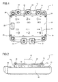
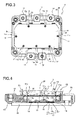
- a semiconductor device 1 according to an embodiment of the present invention illustrated by a plan view in FIG. 1 and a side view in FIG. 2 is configured as an intelligent power module (IPM) applied in an inverter device, in which a control circuit board 20 is provided on an outer case 10 that is made from a resin and accommodates a power semiconductor element (chip).
- the control circuit board 20 has a rectangular shape in a plan view, in which a plurality of electronic components 21 that forms a driving circuit and a control circuit of the power semiconductor element and a connector 22 for external electric connection are mounted on one surface of the board, and pin terminals 23 are extended from the outer case 10.
- the electronic components 21 illustrated are depicted in a simplified manner for better understanding.
- FIG. 3 illustrates a plan view illustrating a state where the control circuit board 20 illustrated in FIG. 1 is removed.
- the semiconductor device 1 includes the shield plate 30 which is provided in a lower portion than the upper end of the outer case 10. That is, the shield plate 30 is accommodated in the outer case 10.
- a plurality of through-holes 31 (not illustrated in the figure) through which the convex portions 11a of the supports 11 pass is formed in the periphery of the shield plate 30.
- the convex portions 11a of the supports 11 pass through the through-holes 31 of the shield plate 30 and protrude toward the control circuit board 20 (the front surface of the shield plate 30).
- the through-hole 31 has a circular shape having such a diameter that the convex portion 11a of the support 11 can be inserted.
- An annular fastener 12 as fixing means of the present invention is attached so as to engage with the protruding convex portion 11a, and the shield plate 30 is fixed to the support 11 by the annular fastener 12.
- FIG. 4 illustrates a cross-sectional view along line IV-IV in FIG. 3 .
- the semiconductor device 1 includes a plurality of semiconductor elements 15 and 16 in the outer case 10 made from a resin.
- the semiconductor elements 15 and 16 may be an insulated gate bipolar transistor (IGBT) and a free wheeling diode (FWD), respectively. These semiconductor elements 15 and 16 are mounted on an insulating substrate 17.
- the insulating substrate 17 includes an insulating layer 17a and conductor layers 17b and 17c formed on both surfaces of the insulating layer 17a.
- the semiconductor elements 15 and 16 are connected to the conductor layer 17b in which a circuit pattern is formed and are connected to a plurality of bonding wires 18, and an inverter circuit, for example, is formed as a primary circuit.
- the primary circuit formed is electrically connected to the terminals 13 and 14 in the portion inserted in the outer case 10 by the bonding wires 18. Moreover, the auxiliary circuit of the semiconductor elements 15 and 16 is electrically connected to the pin terminals 23 by the bonding wires 18.
- the conductor layer 17c of the insulating substrate 17 is bonded to the metal substrate 19 by solders.
- the outer case 10 is attached onto the metal substrate 19.
- the support 11 formed in the outer case 10 includes a convex portion 11a that passes through the through-hole 31 formed in the shield plate 30 and a base portion 11b which is connected to the convex portion 11a and has a larger diameter than the convex portion 11a.
- a flat portion 11c is formed between the convex portion 11a and the base portion 11b.
- the shield plate 30 is placed on the flat portion 11c with the convex portion 11a passing through the shield plate 30, whereby the shield plate 30 is supported.
- the support 11 is provided in the outer case 10 by being molded integrally with the outer case 10.
- the support 11 is not limited to that molded integrally with the outer case 10.
- one or a plurality of supports 11 may be formed on a plate or a frame that is formed separately from the outer case 10, and the plate or the frame may be accommodated in the outer case 10.
- the position in the outer case 10 where the support 11 is formed is a position that is within the outer case 10 and corresponds to the periphery of the shield plate 30.
- the position may be in a central portion of the shield plate 30 as long as the support 11 does not interfere with wires of the semiconductor elements 15 and 16 accommodated in the outer case 10.
- the support 11 may be provided on the upper end of the outer wall of the outer case 10.
- the support 11 is molded integrally with the outer case 10 and is made from the same resin as the outer case 10.
- the support 11 may be made from metal.
- the support 11 is preferably made from a resin.
- the support 11 may be configured such that the distal end of the convex portion 11a is not in contact with the control circuit board 20, and in this case, it is not necessary to take insulation of the metal support 11 into consideration.
- the height h of the convex portion 11a of the support 11 is longer than the thickness of the shield plate 30 and has such a length that the convex portion 11a protrudes through the through-hole 31 of the shield plate 30. Specifically, the height is determined as a length required as the distance between the shield plate 30 placed on the flat portion 11c of the support 11 and the control circuit board 20 that is in contact with the distal end of the convex portion 11a of the support 11.
- the convex portion 11a of the support 11 has an approximately cylindrical shape and has such a tapered shape that narrows as the convex portion 11a advances toward the distal end.
- the diameter of the convex portion 11a of the support 11 may be approximately the same as the diameter of a screw portion of a screw used for screw-clamping a shield plate of a conventional semiconductor device.
- annular fastener 12 attached to the convex portion 11a of the support 11 in order to fix the shield plate 30 to the support 11 has a configuration in which a plurality of claws 12b is formed on the inner circumference of a ring portion 12a as illustrated by a plan view in FIG. 6 .
- a diameter of a circle in contact with distal ends of the respective claws 12b may be slightly smaller than the diameter in the base of a portion of the convex portion 11a of the support 11 protruding from the shield plate 30.
- the annular fastener 12 may be made from metal.
- the claw 12b may have a trapezoidal shape that protrudes toward the center when seen in the plan view as illustrated in FIG.
- annular fastener 12 which has a polygonal hole instead of the claws 12b and in which the diameter of an inscribed circle of the hole is slightly smaller than the diameter in the base of the convex portion 11a and respective sides of the hole bite into the convex portion 11a may be used as the annular fastener 12.
- shape (outer shape) on the outer circumference side of the annular fastener 12 of the present invention is not limited to a circular shape but may be a polygonal shape or the like as long as the respective claws 12b on the inner circumference side of the ring portion 12a bite into the support 11 whereby the shield plate 30 is fixed to the support 11.
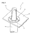
- a state where the annular fastener 12 is attached to the support 11 is illustrated by a schematic perspective view in FIG. 7 .
- the convex portion 11a of the support 11 protrudes through the through-hole 31 of the shield plate 30.
- the annular fastener 12 is moved toward the base of the convex portion 11a along the convex portion 11a protruding through the hollow portion of the annular fastener 12 until the annular fastener 12 comes into contact with the shield plate 30. By doing so, the claws 12b of the annular fastener 12 bite into the convex portion 11a.
- the shield plate 30 is fixed by the convex portion 11a of the support 11 and the annular fastener 12, it is not necessary to screw-clamp the shield plate 30.
- the thickness of the semiconductor device 1 of the present embodiment can be reduced at least by 5 mm as compared to the conventional semiconductor device in which the shield plate 30 is screw-clamped.
- the shield plate 30 can be fixed just by attaching the annular fastener 12 to the convex portion 11a of the support 11, assembling workability is improved as compared to the screw-clamping method. Moreover, since the annular fastener 12 is not expensive, it is possible to reduce the component cost. Further, since the improvement of the outer case 10 is realized by a simple structure of providing the support 11, it is possible to reduce the number of components and the cost as compared to the screw-clamping method. Furthermore, although the screw-clamping method involves forming female screw holes in the screw seats of the outer case, a sealing material may enter into the holes of the screw seats when the semiconductor elements in the outer case are sealed by a sealing resin.
- the support 11 formed on the outer case 10 does not have a hole, and it is not necessary to take entrance of the sealing material into consideration.
- the distal end of the convex portion 11a of the support 11 is configured to make contact with the control circuit board 20.
- the vibration suppressing efficiency of the support 11 is large when the control circuit board 20 has a large size.
- the annular fastener is not limited to a donut-shaped fastener illustrated in FIG. 6 .
- an annular fastener 12A having a larger thickness than the annular fastener illustrated in FIG. 6 may be used.
- a cylindrical annular fastener 12B which has a similar outer shape to the annular fastener 12A and has a straight through-hole as illustrated by a schematic perspective view in FIG. 9 , for example, and which is tightly fitted to the convex portion 11a may be used.
- a cap-shaped annular fastener 12C that covers the convex portion 11a of the support 11 as illustrated by a schematic perspective view in FIG. 10 maybe used.
- the cap-shaped annular fastener 12C preferably has such dimensions that the upper end of the annular fastener 12C comes into contact with the shield plate 30 when the annular fastener 12C is attached to the convex portion 11a of the support 11.
- the shield plate 30 is formed of a plate made from a material such as aluminum, copper, or iron. In order to provide electric insulation, the shield plate 30 is preferably insert-molded from an insulating resin. Polyphenylene sulfide (PPS) or polybutylene terephthalate (PBT) is used as the resin. Moreover, an insulating sheet may be attached to the shield plate 30 instead of the resin. Further, an electromagnetic wave absorbing sheet may be attached to at least one surface of the shield plate 30 instead of the resin.
- PPS polyphenylene sulfide
- PBT polybutylene terephthalate
- At least one of the supports 11 may be made from metal so that the shield plate 30 and the control circuit board are electrically connected.
- FIG. 11 illustrates a cross-sectional view of another embodiment of the present invention.
- the same members as those illustrated in FIG. 4 will be denoted by the same reference numerals, and redundant description thereof will not be provided.
- a semiconductor device 2 of the embodiment illustrated in FIG. 11 is an example in which a convex portion 11Aa of a support 11A has a portion 11Aa1 that protrudes through the through-hole 31 formed in the control circuit board 20.
- the protruding portion 11Aa1 has a smaller diameter than a base portion 11Aa2 of the convex portion on the lower side than the control circuit board 20, and the control circuit board 20 is placed on a flat portion formed in a connection portion between the protruding portion 11Aa1 and the base portion 11Aa2.
- This control circuit board 20 is fixed by the annular fastener 12.
- the shield plate 30 is fixed by the annular fastener 12 having an inner diameter corresponding to the diameter of the base portion 11Aa2 of the convex portion of the support 11A.
- the control circuit board 20 as well as the shield plate 30 can be fixed by the support 11A and the annular fastener 12 together with other screw-clamping and instead of screw-clamping.
- the shield plate 30 is fixed to the support 11 by the annular fastener 12 as fixing means.
- shield plates 30A, 40, 50, 60, and 70 of the second to seventh embodiments described later may be used instead of the shield plate 30 illustrated in FIG. 11 , and the shield plates may be fixed to the support 11 by the claw 31 formed in the through-hole 31 of the shield plates.
- a semiconductor device 3 of the present embodiment is illustrated by a plan view in FIG. 12 and a side view in FIG. 13 .
- FIGS. 12 and 13 the same components as the components of the semiconductor device of the first embodiment illustrated by the plan view in FIG. 1 and the side view in FIG. 2 are denoted by the same reference numerals.
- the semiconductor device 3 of the present embodiment illustrated in FIGS. 12 and 13 has the same appearance as the semiconductor device of the first embodiment illustrated in FIGS. 1 and 2 .
- redundant description of the same portions of the semiconductor device 3 of the present embodiment as those of the semiconductor device 1 of the first embodiment described with reference to FIGS. 1 and 2 will not be provided.
- FIG. 14 illustrates a plan view illustrating a state where the control circuit board 20 illustrated in FIG. 12 is removed.
- the semiconductor device 3 includes a shield plate 30A which is provided on the upper end of the outer case 10 or in a lower portion than the upper end. That is, the shield plate 30A is accommodated in the outer case 10.
- a plurality of through-holes 31 through which the convex portions 11a of the supports 11 pass is formed in the periphery of the shield plate 30A.
- the convex portions 11a of the supports 11 pass through the through-holes 31.
- a claw 31a that engages with the convex portion 11a is formed in the through-hole 31 as fixing means, which will be described in detail later.
- FIG. 15 illustrates a cross-sectional view along line XV-XV in FIG. 14 .
- the semiconductor device 3 of the present embodiment illustrated in FIG. 15 is different from the semiconductor device 1 of the first embodiment in that the claw 31a (see FIG. 18 ) formed in the through-hole 31 of the shield plate 30A engages with the convex portion 11a of the support 11, whereby the shield plate 30A is fixed to the support 11.
- the semiconductor device 3 of the present embodiment illustrated in FIG. 15 has the same configuration as the semiconductor device 1 illustrated in FIG. 4 , and the same components as those of the semiconductor device 1 illustrated in FIG. 4 are denoted by the same reference numerals.
- redundant description of the same portions of the semiconductor device 3 of the present embodiment illustrated in FIG. 15 as those described with reference to FIG. 4 will not be provided.
- the support 11 provided in the outer case 10 of the semiconductor device 3 of the present embodiment is the same as the support 11 provided in the outer case 10 of the semiconductor device 1 of the first embodiment illustrated in FIG. 5 .
- redundant description of the same portion of the support of the semiconductor device 3 of the present embodiment as that described with reference to FIG. 5 and other figures will not be provided.
- a plurality of claws 31a extending toward the center from the peripheral surface of the through-hole 31 is formed in the through-hole 31 of the shield plate 30A as fixing means for fixing the shield plate 30A to the support 11.
- the claws 31a can be formed by performing drilling such as punching when forming the through-holes 31 in the shield plate 30A made from an electromagnetic shielding material such as aluminum, copper, or iron so that the holes have a shape illustrated in FIG. 16 .
- the diameter of an imaginary circle making contact with the distal ends of the claws 31a may be slightly smaller than the diameter in the base of the convex portion 11a connected to the flat portion 11c of the support 11.
- the claw 31a may have a trapezoidal shape that protrudes toward the center when seen in the plan view as illustrated in FIG. 16 and may have a triangular shape, a quadrangular shape, or a circular arc shape that protrudes toward the center, for example.
- the fixing means may be configured such that the through-hole 31 may have a polygonal shape in a plan view, the diameter of an inscribed circle of the polygon may be slightly smaller than the diameter in the base of the convex portion 11a, and the inner surface of the polygonal through-hole 31 bites into the convex portion 11a.
- the annular fastener 12 (see FIG. 6 ) which is prepared separately from the shield plate 30A and has claws engaging with the convex portion 11a that protrudes through the through-hole 31 of the shield plate 30A may be used additionally.
- FIG. 17 illustrates a schematic perspective view illustrating a state where the shield plate 30A is fixed to the support 11 by the claws 31a of the through-hole 31.
- the semiconductor device 3 of the present embodiment since the shield plate 30A is fixed by the convex portion 11a of the support 11 and the claws 31a of the shield plate 30A, it is not necessary to screw-clamp the shield plate 30A.
- the semiconductor device 3 can save the height of screws, and it is not necessary to create insulation distance for metal screws. Therefore, it is possible to reduce the thickness and the size of the semiconductor device 3 as compared to when the shield plate 30A is screw-clamped.
- the thickness of the semiconductor device 3 of the present embodiment can be reduced at least by 5 mm as compared to the conventional semiconductor device in which the shield plate 30A is screw-clamped.
- the shield plate 30A can be fixed just by attaching the shield plate 30A having the through-hole 31 in which the claws 31a are formed to the convex portion 11a of the support 11, assembling workability is improved as compared to the screw-clamping method. Moreover, since it is easy to create the hole shape of the through-hole 31 of the shield plate 30A, it is possible to reduce the component cost. Further, since the improvement of the outer case 10 is realized by a simple structure of providing the support 11, it is possible to reduce the number of components and the cost as compared to the screw-clamping method.
- the method of screw-clamping the shield plate 30A to the outer case 10 involves forming female screw holes in the screw seats formed in the outer case 10, a sealing material that seals semiconductor elements in the outer case may enter into the holes of the screw seats. Due to this, the screw seats are formed at a higher position such that the sealing material does not enter into the screw seats. In this respect, it is difficult to reduce the height of the shield plate and the height of the outer case. In contrast, in the semiconductor device 3 of the present embodiment, the support 11 formed on the outer case 10 does not have a hole, and it is not necessary to take entrance of the sealing material into consideration. Thus, it is possible to provide the shield plate 30A in the outer case 10 and to reduce the height of the outer case.
- the distal end of the convex portion 11a of the support 11 is configured to make contact with the control circuit board 20.
- the vibration suppressing efficiency of the support 11 is large when the control circuit board 20 has a large size.
- FIG. 18 illustrates a plan view of an example of the shield plate 30A.
- the shield plate 30A illustrated has an approximately rectangular shape in a plan view, in which two or three through-holes 31 are formed on the long side and one through-hole 31 is formed on the short side.
- the shield plate 30A is formed of a plate made from a material such as aluminum, copper, or iron.
- the shield plate 30A is preferably insert-molded or coated with an insulating resin.
- PPS polyphenylene sulfide
- PBT polybutylene terephthalate
- an insulating sheet may be attached to the shield plate 30A instead of the resin.
- an electromagnetic wave absorbing sheet may be attached to at least one surface of the shield plate 30A instead of the resin.
- At least one of the plurality of supports 11 may be made from metal so that the shield plate 30A and the control circuit board 20 are electrically connected.
- the semiconductor device of the fourth embodiment has the same configuration as the semiconductor device 3 of the third embodiment except for a shield plate 40 described below. That is, the semiconductor device of the fourth embodiment uses the shield plate 40 instead of the shield plate 30A of the semiconductor device 3 of the third embodiment.
- the semiconductor device of the fourth embodiment includes the outer case 10 in which the support 11 is provided and the control circuit board 20 similarly to the semiconductor device 3 of the third embodiment, and the shield plate 40 having the same shielding property as the shield plate 30A of the semiconductor device 3 of the third embodiment is fixed to the support 11.
- the shield plate 40 which is the difference from the semiconductor device 3 of the third embodiment will be described.
- FIG. 19 illustrates a plan view of the shield plate 40 of the semiconductor device according to the present embodiment.
- the shield plate 40 illustrated in FIG. 19 has an approximately rectangular shape in a plan view, and includes the through-hole 31 through which the convex portion 11a of the support 11 formed in the outer case 10 passes similarly to the shield plate 30A of the third embodiment illustrated in FIG. 18 .
- a plurality of claws 31a extending toward the center from the peripheral surface of the through-hole 31 is formed in the through-hole 31 similarly to the through-hole 31 illustrated in FIG. 16 .
- a slit 32 is formed around the through-hole 31 of the shield plate 40. The slit 32 is the difference from the shield plate 30A of the third embodiment.
- the slit 32 illustrated in FIG. 19 is a groove that penetrates from one surface of the shield plate 40 to the other surface.
- the slit 32 has such a plan-view shape that includes a central portion 32a formed at a position closer to the center of the shield plate 40 than the through-hole 31 and having a circular arc-shape of which the center is located substantially at the same position as the through-hole 31 and an end portion 32b connected to the ends of the central portion 32a so as to extend in parallel to an adjacent edge of the shield plate 40.
- the slit 32 facilitates an operation of inserting the convex portion 11a of the support 11 into the through-hole 31 when the shield plate 40 is attached to the outer case 10 during assembling of the semiconductor device.
- the convex portion 11a of the support 11 is inserted into the through-hole 31, it is necessary to align the convex portion 11a of the support 11 with the through-hole 31 of the shield plate 40.
- a structure in which the claws 31a are formed in the through-hole 31 and engage with the convex portion 11a requires high alignment accuracy.
- the convex portions 11a of the supports 11 corresponding to the through-holes 31 arranged along one side of the respective sides of the approximately rectangular shield plate 40 may be inserted into the through-holes 31, and then, the convex portions 11a of the supports 11 may be inserted into the through-holes 31 arranged along the other side.
- the shield plate 40 is inclined with respect to the upper surface of the outer case 10
- the position of the through-holes 31 arranged along the other side is shifted from the position of the convex portions 11a of the supports 11 corresponding to the through-holes.
- Even if the shift amount is small, it may be difficult to realize alignment.
- the shift amount is large and it is difficult to realize alignment.
- the shield plate 40 has the slits 32 formed near the through-holes 31 at positions closer to the center of the shield plate than the through-holes 31, the portions near the through-holes 31 of the shield plate 40 are likely to be elastically deformed when force is applied. Specifically, when force is applied toward the center from one side of the shield plate 40, the portions are elastically deformed so that the width of the slit 32 formed at the position closer to the center than the through-hole 31 decreases. With this elastic deformation, the positions of the through-holes 31 are moved toward the center.
- the slits 32 are formed at the positions near the through-holes 31, the portions near the through-holes 31 of the shield plate 40 can be moved with elastic deformation. More preferably, as illustrated in FIG. 19 , the slits 32 may be formed near the through-holes 31 at positions closer to the center of the shield plate 40 than the through-holes 31.
- the slits 32 are not limited to the example in which the slits 32 are formed near all through-holes 31 formed in the shield plate 40, but the slits 32 may be formed near some of the through-holes 31. However, it is preferable that the slits 32 are formed near all through-holes 31.
- the slit 32 includes the circular arc-shaped central portion 32a and the linear end portion 32b. This is because, although the present embodiment includes a mode in which the slit 32 is formed only of the central portion 32a, a crack may appear toward the end of the shield plate 40 from the ends of the central portion 32a in the slit formed only of the central portion 32a, and in addition, the movable range when force is applied to the shield plate 40 is small, and the elastic deformation amount is small.
- the movable range can be increased by increasing the size of the circular arc-shaped central portion 32a, if the size of the central portion 32a is increased such that the central portion 32a is positioned immediately above the semiconductor element (semiconductor chip) accommodated in the outer case 10, the shielding property of the shield plate 40 may decrease.
- a shape in which the linear end portions 32b are formed so as to be connected to the ends of the central portion 32a as illustrated in FIG. 19 it is possible to prevent cracks, to increase the movable range, and to increase the elastic deformation amount.
- the central portion 32a of the slit 32 is not limited to a circular arc-shape illustrated in FIG. 19 , and two sides of a triangle or three sides of a quadrangle may form the central portion 32a.
- FIG. 20 illustrates a plan view of a semiconductor device 5 of the present embodiment in which an insulating circuit board is removed.
- the semiconductor device 5 illustrated has the same configuration as the semiconductor device 3 of the third embodiment except for a shield plate 50 described below. That is, the semiconductor device of the fifth embodiment uses the shield plate 50 instead of the shield plate 30A of the semiconductor device 3 of the third embodiment.
- the semiconductor device of the fifth embodiment includes the outer case 10 in which the support 11 is formed and the control circuit board 20 (not illustrated) similarly to the semiconductor device of the third embodiment, in which the shield plate 50 having the same shielding property as the shield plate 30A of the semiconductor device 3 of the third embodiment is fixed to the support 11.
- the shield plate 50 having the same shielding property as the shield plate 30A of the semiconductor device 3 of the third embodiment is fixed to the support 11.
- FIG. 21 illustrates a plan view of the shield plate 50 of the semiconductor device 5 according to the present embodiment.
- the shield plate 50 illustrated in FIG. 21 has an approximately rectangular shape in a plan view, in which the through-hole 33 through which the convex portion 11a of the support 11 formed in the outer case 10 passes is formed.
- a notch 34 cut from the edge of the shield plate 50 is connected to the through-hole 33.
- Claws 33a that extend toward the center from the peripheral surface of the through-hole 33 are formed in the half of the circumference of the through-hole 33 as fixing means.
- the claws 33a engage with the convex portion 11a of the support 11, whereby the shield plate 50 is fixed to the support 11.
- the notch 34 formed between the through-hole 33 of the shield plate 50 and the edge of the shield plate 50 illustrated in FIG. 21 facilitates the operation of inserting the convex portion 11a of the support 11 into the through-hole 33 when the shield plate 50 is attached to the outer case 10 during assembling of the semiconductor device.
- the convex portions 11a of the supports 11 corresponding to the through-holes 33 arranged along one side of the respective sides of the approximately rectangular shield plate 50 may be inserted into the through-holes 33, and then, the convex portions 11a of the supports 11 may be inserted into the through-holes 33 arranged along the other side.
- the notch 34 in order to facilitate the alignment between the through-holes 33 and the convex portions 11a of the supports 11, the notch 34 has such a shape that the width increases gradually as the notch advances from the through-hole 33 toward the end of the shield plate 40.
- the plan-view shape of the notch 34 is not limited to the shape illustrated in FIG. 21 as long as the notch 34 can guide the convex portion 11a.
- the shield plate 50 illustrated in FIG. 21 has the slits 32 formed near the through-holes 33 at positions closer to the center of the shield plate 50 than the through-holes 33.
- the slit 32 illustrated in FIG. 21 has the same configuration as the slit 32 of the shield plate 40 described with reference to FIG. 19 in the fourth embodiment and provides the same advantageous effects. Thus, redundant description of the slit 32 described in the fourth embodiment will not be provided.
- the shield plate 50 of the present embodiment includes the notches 34 connected to the through-holes 33 and the slits 32, by the synergy of the notches 34 and the slits 32, the operation of inserting the convex portions 11a of the supports 11 into the through-holes 33 when attaching the shield plate 50 to the outer case 10 during assembling of the semiconductor device is facilitated.
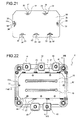
- FIG. 22 illustrates a plan view of a semiconductor device 6 of the present embodiment
- FIG. 23 illustrates a cross-sectional view along line XXIII-XXIII of the semiconductor device 6 illustrated in FIG. 22.
- FIGS. 22 and 23 illustrate the semiconductor device 6 in the state where the control circuit board 20 is removed.
- FIGS. 22 and 23 are diagrams corresponding to FIGS. 14 and 15 of the third embodiment described above, and the same components as those of FIGS. 14 and 15 are denoted by the same reference numerals. Thus, in the following description, description of the same components of the semiconductor device 6 of the sixth embodiment as those described in the third embodiment will not be provided.
- the semiconductor device 6 of the present embodiment illustrated in FIGS. 22 and 23 has the same configuration as the semiconductor device 3 of the third embodiment illustrated in FIGS. 14 and 15 except for a shield plate 60 described below. That is, the semiconductor device 6 of the sixth embodiment uses the shield plate 60 instead of the shield plate 3 of the semiconductor device 3 of the third embodiment.
- the semiconductor device 6 of the sixth embodiment includes the outer case 10 in which the support 11 is provided and the control circuit board 20 similarly to the semiconductor device 3 of the third embodiment, and the shield plate 60 having the same shielding property as the shield plate 30A of the semiconductor device 3 of the third embodiment is fixed to the support 11.
- FIGS. 24A and 24B illustrate a plan view ( FIG. 24A ) and a cross-sectional view ( FIG. 24B ) of the shield plate 60 of the semiconductor device 6 of the present embodiment.
- the shield plate 60 illustrated in FIGS. 24A and 24B has an approximately rectangular shape in a plan view, and includes the through-hole 31 through which the convex portion 11a of the support 11 formed in the outer case 10 passes similarly to the shield plate 30A of the third embodiment illustrated in FIG. 18 .
- a plurality of claws 31a extending toward the center from the peripheral surface of the through-hole 31 is formed in the through-hole 31 similarly to the through-hole 31 illustrated in FIG. 16 .
- a convex portion 35 is formed on a surface of the shield plate 60 on the side (see FIG. 23 ) closer to the semiconductor elements (chips) 15 and 16 when the shield plate 60 is attached to the outer case 10.
- the convex portion 35 is the difference from the shield plate 30A of the third embodiment.
- the convex portions 35 illustrated in FIG. 24 are two linear portions (protruding strips or projections) extending in parallel along the longitudinal direction of the shield plate 60.
- the convex portions 35 can be formed by press-processing the shield plate 60, for example.
- the convex portion 35 has a structure in which a distal end is in contact with a sealing material 36 filled in the outer case 10.
- the convex portion 35 may have a structure in which the distal end is in contact with a member provided in the outer case.
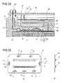
- FIG. 25 illustrates a cross-sectional view of a semiconductor device having a busbar block 25.
- the busbar block 25 has a structure (block structure) in which a portion of a busbar 25a connected to the conductor layer 17b or the like of the insulating substrate 17 is wrapped by a block 25b, and the busbar block 25 is provided above the semiconductor elements (chips) 15 and 16.
- the busbar 25a is formed of a plate member made from copper, aluminum, or the like, and the block 25b is formed from an insulating material such as resin or ceramics. In the semiconductor device illustrated in FIG. 25 , the convex portion 35 of the shield plate 60 is connected to the busbar block 25.
- the fixing means is not limited to the claws 31a of the through-holes 31.
- the annular fastener 12 illustrated in FIG. 6 may be used instead of the claws 31a of the through-holes 31 or together with the claws 31 of the through-holes 31.
- the shield plate having the convex portions 35 is not limited to the shield plate 60 illustrated in FIGS. 24A and 24B .
- a shield plate in which the convex portions 35 of the shield plate 60 illustrated in FIGS. 24A and 24B is formed on the shield plate 30 of the semiconductor device 1 of the first embodiment illustrated in FIG. 3 may be used.
- the claws 31a of the through-holes 31 which is the fixing means for fixing the shield plate 60 to the supports 11 are not always necessarily provided in all through-holes 31 that are formed in the shield plate 60.
- the claws 31a may be provided in some of the through-holes 31 formed in the shield plate 60, and screws for fixing the supports 11 may be provided in the remaining through-holes so that the shield plate 60 is partially screw-clamped.
- the semiconductor device of the seventh embodiment has the same configuration as the semiconductor device 6 of the sixth embodiment except for a shield plate 70 described below. That is, the semiconductor device of the seventh embodiment uses the shield plate 70 instead of the shield plate 60 of the sixth embodiment.
- the semiconductor device of the seventh embodiment includes the outer case 10 in which the support 11 is provided and the control circuit board 20 (not illustrated) similarly to the semiconductor device 6 of the sixth embodiment, and the shield plate 70 having the same shielding property as the shield plate 60 of the semiconductor device of the sixth embodiment is fixed to the support 11.
- the shield plate 70 which is the difference from the semiconductor device 6 of the sixth embodiment will be described.
- FIGS. 26A and 26B illustrate a plan view ( FIG. 26A ) and a cross-sectional view ( FIG. 26B ) of the shield plate 70.
- the shield plate 70 illustrated in FIGS. 26A and 26B has an approximately rectangular shape in a plan view, and includes the through-hole 31 through which the convex portion 11a of the support 11 formed in the outer case 10 passes similarly to the shield plate 60 of the sixth embodiment illustrated in FIGS. 24A and 24B .
- a plurality of claws 31a extending toward the center from the peripheral surface of the through-hole 31 is formed in the through-hole 31 similarly to the through-hole 31 illustrated in FIG. 16 .
- a convex portion 35 is formed on a surface of the shield plate 70 on the side closer to the semiconductor elements (chips) 15 and 16 when the shield plate 70 is attached to the outer case 10. This is the same as the shield plate 60 of the sixth embodiment illustrated in FIGS. 24A and 24B . Further, the shield plate 70 includes the slit 32 that is formed around the through-hole 31. The slit 32 is the difference from the shield plate 60 of the sixth embodiment.
- the slits 32 are formed near the through-holes 31 at positions closer to the center of the shield plate 70 than the through-holes 31.
- the slit 32 of the present embodiment illustrated in FIGS. 26A and 26B has the same configuration as the slit 32 of the shield plate 40 described with reference to FIG. 19 in the fourth embodiment and provides the same advantageous effects. Thus, redundant description of the slit 32 described in the fourth embodiment will not be provided.
- the shield plate 70 of the present embodiment provides a vibration suppressing effect, a thermal deformation suppressing effect, and a heat radiation effect due to the convex portions 35.
- the slits 32 allow the convex portions 11a of the supports 11 to be easily aligned with respect to the positions of the through-holes 31. Further, it is possible to facilitate the operation of inserting the convex portions 11a of the supports 11 into the through-holes 31.
- the supports 11 for fixing the shield plate 70 may be provided on the upper surface of the busbar block 25 illustrated in FIG. 25 .
- the supports 11 provided on the upper surface of the busbar block 25 have lower positional accuracy than the supports 11 provided on the outer case 11.
- the shield plate 70 preferably has the slits 32 because, when the supports 11 for fixing the shield plate 70 are formed on the upper surface of the busbar block 25, the operation of inserting the convex portions 11a of the supports 11 provided on the upper surface of the busbar block 25 into the through-holes 31 is facilitated.
- FIGS.27A to 27F illustrate modifications of the shield plate 70.
- the shield plates 70A to 70F illustrated in FIGS. 27A to 27F are example in which the positions and the number of convex portions 35 are different as compared to the shield plate 70 illustrated in FIGS. 26A and 26B .
- the convex portions 35 are three linear portions extending in parallel along the longitudinal direction of the shield plate 70A and are arranged in two lines in the longitudinal direction of the shield plate 70A.
- the convex portions 35 are three linear portions extending in parallel along the longitudinal direction of the shield plate 70B.
- the convex portions 35 are X-shaped portions extending in a diagonal direction of the shield plate 70E.
- the convex portions 35 are a combination of three linear portions extending in parallel along the longitudinal direction of the shield plate 70F and two linear portions provided with these convex portions interposed so as to extend in parallel along the lateral direction of the shield plate 70F.
- the convex portions 35 are four linear portions extending in parallel along the longitudinal direction of the shield plate 70C, and the convex portions located close to the ends are arranged in two lines in the longitudinal direction of the shield plate 70C.
- the convex portions 35 are four linear portions extending in parallel along the longitudinal direction of the shield plate 70D. The positions and the number of convex portions 35 can be appropriately changed according to an inner structure of the outer case 10.
Landscapes
- Engineering & Computer Science (AREA)
- Microelectronics & Electronic Packaging (AREA)
- Shielding Devices Or Components To Electric Or Magnetic Fields (AREA)
- Inverter Devices (AREA)
- Refuge Islands, Traffic Blockers, Or Guard Fence (AREA)
- Physics & Mathematics (AREA)
- Health & Medical Sciences (AREA)
- Electromagnetism (AREA)
- Toxicology (AREA)
Abstract
Description
- The present invention relates to a semiconductor device, and more particularly, to a semiconductor device in which a control circuit board is fixed to an outer case that accommodates a power semiconductor element.
- A semiconductor module in which a power semiconductor element such as an insulated gate bipolar transistor (IGBT) is built into an outer case made from a resin is known as an example of a semiconductor device that controls a motor or the like. A semiconductor module including a control circuit board that controls a power semiconductor element is also known. In a power semiconductor module that includes a control circuit board, noise generated during a switching operation of a power semiconductor element may have an influence on the control circuit board and the power semiconductor element. Thus, the control circuit board is fixed to the outer case to be separated from the power semiconductor element such that the influence of noise does not reach. The control circuit board is fixed to an outer side of the outer case by screw-clamping, for example.
- Higher operating speed, smaller size, and lower power consumption required for recent electronic devices are severe requirements for noise resistance of electronic devices against external noise. Moreover, the sources of external noise are ever increasing, and the demand for noise resistance of electronic devices becomes stronger as well as removal of interfering noise, which has been demanded in the past. In particular, on-vehicle electronic devices (on-vehicle intelligent power modules and the like) used in severe environments require stricter anti-noise countermeasures than the conventional level because of the requirements demanded by manufacturers.
- Thus, anti-noise countermeasures are taken on a control circuit board for controlling a power semiconductor element or the like, or a shield plate is arranged between the power semiconductor element and the control circuit board. As the former anti-noise countermeasures on the control circuit board side, a metal foil is attached to the entire surface of the control circuit board close to the outer case and is electrically connected to the ground, or circuits or patterns are designed as anti-noise countermeasures, or components for anti-noise countermeasures such as capacitors are provided.
- As the latter anti-noise countermeasures of arranging the shield plate, a semiconductor device in which the shield plate is fixed by screw-clamping is known (Patent Literature 1). Moreover, a semiconductor device in which a print board having a shield layer is fixed by screw-clamping to external connection terminals fixed and supported on an outer case (Patent Literature 2). Moreover, a semiconductor device in which a shield plate is mounted on the ends of step supports implanted in an outer case, a metal ring is placed so that a coupling portion of each of the step supports passes through the metal ring, a control circuit board is mounted on the metal rings, the control circuit board and the shield plate overlapped in two stages are fixed by screw-clamping to the step supports (Patent Literature 3). Since these semiconductor devices have the shield plate arranged between the power semiconductor element and the control circuit board, it is possible to suppress noise radiating from one of the power semiconductor element and the control circuit board from entering into the other by being partially blocked by the shield plate. A metal plate made from a material corresponding the properties of noise is used as the shield plate, and it is possible to effectively block noise.
- Patent Literature 1: Japanese Patent No.
4583122 - Patent Literature 2: Japanese Patent Application Publication No.
2009-130163 - Patent Literature 3:
WO 2010/150471 - The semiconductor devices disclosed in
Patent Literature 1 to 3 use metal screws or metal rings in order to fix the shield plate. Thus, since metal components are used, it is necessary to design by taking a separation distance between the shield plate and the control circuit board mounted above the shield plate into consideration and to prepare a void distance corresponding to a screw height between the shield plate and the control circuit board. Therefore, the overall height of the semiconductor device having the control circuit board increases and the volume increases. - The present invention solves the above problems advantageously, and an object thereof is to provide a semiconductor device having a control circuit board, capable of fixing a shield plate without using screws and reducing the thickness and the size.
- In order to attain the object, a semiconductor device having the following configuration is provided.
- The semiconductor device includes: a semiconductor element accommodated in an outer case; a control circuit board fixed to the outer case to be separated from the semiconductor element; and a shield plate provided between the semiconductor element and the control circuit board. The outer case is provided with a support having a convex portion longer than a thickness of the shield plate at a distal end thereof. A through-hole through which the convex portion of the support passes is formed in the shield plate. The shield plate is fixed to the support by fixing means that engages with the convex portion.
- According to the present invention, the support is provided on the outer case in which the semiconductor element is accommodated, the convex portion of the support passes through the shield plate, and the shield plate is fixed to the support by the fixing means that engages with the convex portion. Thus, the shield plate can be fixed without using screws. Therefore, it is possible to reduce the thickness and the size of the semiconductor device having the control circuit board.
-
-
FIG. 1 is a plan view of an embodiment of a semiconductor device according to the present invention. -
FIG. 2 is a side view of the semiconductor device illustrated inFIG. 1 . -
FIG. 3 is a plan view illustrating a state where a control circuit board illustrated inFIG. 1 is removed. -
FIG. 4 is a cross-sectional view along line IV-IV inFIG. 3 . -
FIG. 5 is a perspective view of a support. -
FIG. 6 is a plan view of an annular fastener. -
FIG. 7 is a perspective view when the annular fastener is attached to thesupport 11. -
FIG. 8 is a schematic perspective view illustrating another example of the annular fastener. -
FIG. 9 is a schematic perspective view illustrating another example of the annular fastener. -
FIG. 10 is a schematic perspective view illustrating another example of the annular fastener. -
FIG. 11 is a cross-sectional view illustrating another embodiment of the present invention. -
FIG. 12 is a plan view of a semiconductor device according to a third embodiment of the present invention. -
FIG. 13 is a side view of a semiconductor device illustrated inFIG. 12 . -
FIG. 14 is a plan view illustrating a state where a control circuit board illustrated inFIG. 12 is removed. -
FIG. 15 is a cross-sectional view along line XV-XV inFIG. 14 . -
FIG. 16 is an enlarged view of a portion of a shield plate. -
FIG. 17 is a perspective view illustrating a state where a shield plate is attached to a support. -
FIG. 18 is a plan view of a shield plate of the semiconductor device according to the third embodiment of the present invention. -
FIG. 19 is a plan view of a shield plate of a semiconductor device according to a fourth embodiment of the present invention. -
FIG. 20 is a plan view of a semiconductor device according to a fifth embodiment of the present invention. -
FIG. 21 is a plan view of a shield plate of the semiconductor device according to the fifth embodiment of the present invention. -
FIG. 22 is a plan view of a semiconductor device according to a sixth embodiment of the present invention. -
FIG. 23 is a cross-sectional view along line XXIII-XXIII inFIG. 22 . -
FIGS. 24A and 24B are diagrams for describing a shield plate of the semiconductor device according to the sixth embodiment of the present invention. -
FIG. 25 is a cross-sectional view of a semiconductor device having a busbar. -
FIGS. 26A and 26B are plan views of a shield plate of a semiconductor device according to a seventh embodiment of the present invention. -
FIGS. 27A to 27F are plan views illustrating modifications of the shield plate illustrated inFIGS. 26A and 26B . - Embodiments of the semiconductor device of the present invention will be described in detail with reference to the drawings.
- A
semiconductor device 1 according to an embodiment of the present invention, illustrated by a plan view inFIG. 1 and a side view inFIG. 2 is configured as an intelligent power module (IPM) applied in an inverter device, in which acontrol circuit board 20 is provided on anouter case 10 that is made from a resin and accommodates a power semiconductor element (chip). Thecontrol circuit board 20 has a rectangular shape in a plan view, in which a plurality ofelectronic components 21 that forms a driving circuit and a control circuit of the power semiconductor element and aconnector 22 for external electric connection are mounted on one surface of the board, andpin terminals 23 are extended from theouter case 10. Theelectronic components 21 illustrated are depicted in a simplified manner for better understanding. - A wiring pattern (not illustrated) formed from conductive metal and connected to the plurality of
electronic components 21 is formed on the other surface (rear surface) of thecontrol circuit board 20. Thecontrol circuit board 20 is fixed to theouter case 10 by screwingscrews 24 attached to four corners of thecontrol circuit board 20 to screwseats 10a (seeFIG. 2 ) formed on the upper end on the front surface side of theouter case 10. Referring toFIG. 2 , distal ends of convex (projection)portions 11a of pin-shapedsupports 11 protruding toward the front surface from theouter case 10 are in contact with the rear surface of thecontrol circuit board 20 fixed by thescrews 24. In this way, vibration of thecontrol circuit board 20 is suppressed. Thesupport 11 which will be described later is used for fixing ashield plate 30 illustrated inFIG. 3 by anannular fastener 12. A plurality of terminals (screw terminals) 13 and 14 electrically connected to the power semiconductor element (chip) and the like in theouter case 10 is exposed from the upper end of theouter case 10. -
FIG. 3 illustrates a plan view illustrating a state where thecontrol circuit board 20 illustrated inFIG. 1 is removed. Thesemiconductor device 1 includes theshield plate 30 which is provided in a lower portion than the upper end of theouter case 10. That is, theshield plate 30 is accommodated in theouter case 10. A plurality of through-holes 31 (not illustrated in the figure) through which theconvex portions 11a of thesupports 11 pass is formed in the periphery of theshield plate 30. Theconvex portions 11a of thesupports 11 pass through the through-holes 31 of theshield plate 30 and protrude toward the control circuit board 20 (the front surface of the shield plate 30). In the present embodiment, the through-hole 31 has a circular shape having such a diameter that theconvex portion 11a of thesupport 11 can be inserted. Anannular fastener 12 as fixing means of the present invention is attached so as to engage with the protrudingconvex portion 11a, and theshield plate 30 is fixed to thesupport 11 by theannular fastener 12. -
FIG. 4 illustrates a cross-sectional view along line IV-IV inFIG. 3 . Thesemiconductor device 1 includes a plurality ofsemiconductor elements outer case 10 made from a resin. Thesemiconductor elements semiconductor elements substrate 17. The insulatingsubstrate 17 includes an insulatinglayer 17a and conductor layers 17b and 17c formed on both surfaces of the insulatinglayer 17a. Thesemiconductor elements conductor layer 17b in which a circuit pattern is formed and are connected to a plurality ofbonding wires 18, and an inverter circuit, for example, is formed as a primary circuit. The primary circuit formed is electrically connected to theterminals outer case 10 by thebonding wires 18. Moreover, the auxiliary circuit of thesemiconductor elements pin terminals 23 by thebonding wires 18. Theconductor layer 17c of the insulatingsubstrate 17 is bonded to themetal substrate 19 by solders. Theouter case 10 is attached onto themetal substrate 19. - As illustrated by a perspective view in
FIG. 5 , thesupport 11 formed in theouter case 10 includes aconvex portion 11a that passes through the through-hole 31 formed in theshield plate 30 and abase portion 11b which is connected to theconvex portion 11a and has a larger diameter than theconvex portion 11a. Aflat portion 11c is formed between theconvex portion 11a and thebase portion 11b. Theshield plate 30 is placed on theflat portion 11c with theconvex portion 11a passing through theshield plate 30, whereby theshield plate 30 is supported. - The
support 11 is provided in theouter case 10 by being molded integrally with theouter case 10. However, thesupport 11 is not limited to that molded integrally with theouter case 10. For example, one or a plurality ofsupports 11 may be formed on a plate or a frame that is formed separately from theouter case 10, and the plate or the frame may be accommodated in theouter case 10. In the present embodiment illustrated inFIG. 3 , the position in theouter case 10 where thesupport 11 is formed is a position that is within theouter case 10 and corresponds to the periphery of theshield plate 30. However, the position may be in a central portion of theshield plate 30 as long as thesupport 11 does not interfere with wires of thesemiconductor elements outer case 10. Moreover, thesupport 11 may be provided on the upper end of the outer wall of theouter case 10. - The
support 11 is molded integrally with theouter case 10 and is made from the same resin as theouter case 10. Thesupport 11 may be made from metal. When thesupport 11 is made from metal, in the present embodiment, since the distal end of theconvex portion 11a is in contact with thecontrol circuit board 20, it is necessary to take insulation between thesupport 11 and thecontrol circuit board 20 into consideration. Thus, thesupport 11 is preferably made from a resin. Thesupport 11 may be configured such that the distal end of theconvex portion 11a is not in contact with thecontrol circuit board 20, and in this case, it is not necessary to take insulation of themetal support 11 into consideration. - The height h of the
convex portion 11a of thesupport 11 is longer than the thickness of theshield plate 30 and has such a length that theconvex portion 11a protrudes through the through-hole 31 of theshield plate 30. Specifically, the height is determined as a length required as the distance between theshield plate 30 placed on theflat portion 11c of thesupport 11 and thecontrol circuit board 20 that is in contact with the distal end of theconvex portion 11a of thesupport 11. Theconvex portion 11a of thesupport 11 has an approximately cylindrical shape and has such a tapered shape that narrows as theconvex portion 11a advances toward the distal end. The diameter of theconvex portion 11a of thesupport 11 may be approximately the same as the diameter of a screw portion of a screw used for screw-clamping a shield plate of a conventional semiconductor device. - In the
support 11 illustrated inFIG. 5 , thebase portion 11b has a cylindrical shape having the same central axis as theconvex portion 11a. Thebase portion 11b of thesupport 11 is not limited to the shape illustrated but may have a prismatic shape and other shape as long as thebase portion 11b has a larger cross-sectional area than theconvex portion 11a and theflat portion 11c is formed in the portion connected to theconvex portion 11a. The diameter of thebase portion 11b may be approximately the same as the diameter of a nut coupled with a screw used for screw-clamping a shield plate of a conventional semiconductor device, for example. - An example of the
annular fastener 12 attached to theconvex portion 11a of thesupport 11 in order to fix theshield plate 30 to thesupport 11 has a configuration in which a plurality ofclaws 12b is formed on the inner circumference of aring portion 12a as illustrated by a plan view inFIG. 6 . A diameter of a circle in contact with distal ends of therespective claws 12b may be slightly smaller than the diameter in the base of a portion of theconvex portion 11a of thesupport 11 protruding from theshield plate 30. Theannular fastener 12 may be made from metal. Theclaw 12b may have a trapezoidal shape that protrudes toward the center when seen in the plan view as illustrated inFIG. 6 and may have a triangular shape that protrudes toward the center, for example. Moreover, an annular fastener which has a polygonal hole instead of theclaws 12b and in which the diameter of an inscribed circle of the hole is slightly smaller than the diameter in the base of theconvex portion 11a and respective sides of the hole bite into theconvex portion 11a may be used as theannular fastener 12. Moreover, the shape (outer shape) on the outer circumference side of theannular fastener 12 of the present invention is not limited to a circular shape but may be a polygonal shape or the like as long as therespective claws 12b on the inner circumference side of thering portion 12a bite into thesupport 11 whereby theshield plate 30 is fixed to thesupport 11. - A state where the
annular fastener 12 is attached to thesupport 11 is illustrated by a schematic perspective view inFIG. 7 . Theconvex portion 11a of thesupport 11 protrudes through the through-hole 31 of theshield plate 30. Theannular fastener 12 is moved toward the base of theconvex portion 11a along theconvex portion 11a protruding through the hollow portion of theannular fastener 12 until theannular fastener 12 comes into contact with theshield plate 30. By doing so, theclaws 12b of theannular fastener 12 bite into theconvex portion 11a. In this way, the movement of theannular fastener 12 in an axial direction of theconvex portion 11a is restricted, and as a result, the movement of theshield plate 30 in the axial direction of theconvex portion 11a is restricted. Thus, theshield plate 30 is fixed to thesupport 11. - In the
semiconductor device 1 of the present embodiment, since theshield plate 30 is fixed by theconvex portion 11a of thesupport 11 and theannular fastener 12, it is not necessary to screw-clamp theshield plate 30. Thus, it is possible to reduce the thickness and the size of thesemiconductor device 1 having thecontrol circuit board 20. Specifically, the thickness of thesemiconductor device 1 of the present embodiment can be reduced at least by 5 mm as compared to the conventional semiconductor device in which theshield plate 30 is screw-clamped. - In the
semiconductor device 1 of the present embodiment, since theshield plate 30 can be fixed just by attaching theannular fastener 12 to theconvex portion 11a of thesupport 11, assembling workability is improved as compared to the screw-clamping method. Moreover, since theannular fastener 12 is not expensive, it is possible to reduce the component cost. Further, since the improvement of theouter case 10 is realized by a simple structure of providing thesupport 11, it is possible to reduce the number of components and the cost as compared to the screw-clamping method. Furthermore, although the screw-clamping method involves forming female screw holes in the screw seats of the outer case, a sealing material may enter into the holes of the screw seats when the semiconductor elements in the outer case are sealed by a sealing resin. Due to this, it is necessary to form the screw seats at a higher position of the outer case so that the sealing material does not enter into the screw seats. In this respect, it is difficult to reduce the height of the shield plate and the height of the outer case. In contrast, in thesemiconductor device 1 of the present embodiment, thesupport 11 formed on theouter case 10 does not have a hole, and it is not necessary to take entrance of the sealing material into consideration. Thus, it is possible to provide theshield plate 30 in theouter case 10 and to reduce the height of the outer case. - Further, in the
semiconductor device 1 of the present embodiment, the distal end of theconvex portion 11a of thesupport 11 is configured to make contact with thecontrol circuit board 20. As a result, it is possible to suppress vibration of thecontrol circuit board 20. In particular, the vibration suppressing efficiency of thesupport 11 is large when thecontrol circuit board 20 has a large size. - The annular fastener is not limited to a donut-shaped fastener illustrated in
FIG. 6 . For example, as illustrated by a schematic perspective view inFIG. 8 , anannular fastener 12A having a larger thickness than the annular fastener illustrated inFIG. 6 may be used. Moreover, a cylindricalannular fastener 12B which has a similar outer shape to theannular fastener 12A and has a straight through-hole as illustrated by a schematic perspective view inFIG. 9 , for example, and which is tightly fitted to theconvex portion 11a may be used. Further, a cap-shaped annular fastener 12C that covers theconvex portion 11a of thesupport 11 as illustrated by a schematic perspective view inFIG. 10 maybe used. The cap-shaped annular fastener 12C preferably has such dimensions that the upper end of the annular fastener 12C comes into contact with theshield plate 30 when the annular fastener 12C is attached to theconvex portion 11a of thesupport 11. - The
shield plate 30 is formed of a plate made from a material such as aluminum, copper, or iron. In order to provide electric insulation, theshield plate 30 is preferably insert-molded from an insulating resin. Polyphenylene sulfide (PPS) or polybutylene terephthalate (PBT) is used as the resin. Moreover, an insulating sheet may be attached to theshield plate 30 instead of the resin. Further, an electromagnetic wave absorbing sheet may be attached to at least one surface of theshield plate 30 instead of the resin. - When it is desirable to electrically connect the
shield plate 30 to the ground line of thecontrol circuit board 20 as anti-noise countermeasures, at least one of thesupports 11 may be made from metal so that theshield plate 30 and the control circuit board are electrically connected. -
FIG. 11 illustrates a cross-sectional view of another embodiment of the present invention. InFIG. 11 , the same members as those illustrated inFIG. 4 will be denoted by the same reference numerals, and redundant description thereof will not be provided. - A
semiconductor device 2 of the embodiment illustrated inFIG. 11 is an example in which a convex portion 11Aa of asupport 11A has a portion 11Aa1 that protrudes through the through-hole 31 formed in thecontrol circuit board 20. The protruding portion 11Aa1 has a smaller diameter than a base portion 11Aa2 of the convex portion on the lower side than thecontrol circuit board 20, and thecontrol circuit board 20 is placed on a flat portion formed in a connection portion between the protruding portion 11Aa1 and the base portion 11Aa2. Thiscontrol circuit board 20 is fixed by theannular fastener 12. Moreover, theshield plate 30 is fixed by theannular fastener 12 having an inner diameter corresponding to the diameter of the base portion 11Aa2 of the convex portion of thesupport 11A. According to the present embodiment illustrated inFIG. 11 , thecontrol circuit board 20 as well as theshield plate 30 can be fixed by thesupport 11A and theannular fastener 12 together with other screw-clamping and instead of screw-clamping. Thus, it is possible to further suppress vibration of thecontrol circuit board 20 and to improve workability in fixing thecontrol circuit board 20. - In the
semiconductor device 2 of the present embodiment illustrated inFIG. 11 , theshield plate 30 is fixed to thesupport 11 by theannular fastener 12 as fixing means. However,shield plates shield plate 30 illustrated inFIG. 11 , and the shield plates may be fixed to thesupport 11 by theclaw 31 formed in the through-hole 31 of the shield plates. - Next, a semiconductor device according to a third embodiment of the present invention will be described.
- A
semiconductor device 3 of the present embodiment is illustrated by a plan view inFIG. 12 and a side view inFIG. 13 . InFIGS. 12 and 13 , the same components as the components of the semiconductor device of the first embodiment illustrated by the plan view inFIG. 1 and the side view inFIG. 2 are denoted by the same reference numerals. Thesemiconductor device 3 of the present embodiment illustrated inFIGS. 12 and 13 has the same appearance as the semiconductor device of the first embodiment illustrated inFIGS. 1 and 2 . Thus, in the description with reference toFIGS. 12 and 13 , redundant description of the same portions of thesemiconductor device 3 of the present embodiment as those of thesemiconductor device 1 of the first embodiment described with reference toFIGS. 1 and 2 will not be provided. -
FIG. 14 illustrates a plan view illustrating a state where thecontrol circuit board 20 illustrated inFIG. 12 is removed. Thesemiconductor device 3 includes ashield plate 30A which is provided on the upper end of theouter case 10 or in a lower portion than the upper end. That is, theshield plate 30A is accommodated in theouter case 10. A plurality of through-holes 31 through which theconvex portions 11a of thesupports 11 pass is formed in the periphery of theshield plate 30A. Theconvex portions 11a of thesupports 11 pass through the through-holes 31. Aclaw 31a that engages with theconvex portion 11a is formed in the through-hole 31 as fixing means, which will be described in detail later. -
FIG. 15 illustrates a cross-sectional view along line XV-XV inFIG. 14 . As compared to the cross-sectional view of thesemiconductor device 1 of the first embodiment illustrated inFIG. 4 , thesemiconductor device 3 of the present embodiment illustrated inFIG. 15 is different from thesemiconductor device 1 of the first embodiment in that theclaw 31a (seeFIG. 18 ) formed in the through-hole 31 of theshield plate 30A engages with theconvex portion 11a of thesupport 11, whereby theshield plate 30A is fixed to thesupport 11. Except for this difference, thesemiconductor device 3 of the present embodiment illustrated inFIG. 15 has the same configuration as thesemiconductor device 1 illustrated inFIG. 4 , and the same components as those of thesemiconductor device 1 illustrated inFIG. 4 are denoted by the same reference numerals. Thus, redundant description of the same portions of thesemiconductor device 3 of the present embodiment illustrated inFIG. 15 as those described with reference toFIG. 4 will not be provided. - Moreover, the
support 11 provided in theouter case 10 of thesemiconductor device 3 of the present embodiment is the same as thesupport 11 provided in theouter case 10 of thesemiconductor device 1 of the first embodiment illustrated inFIG. 5 . Thus, redundant description of the same portion of the support of thesemiconductor device 3 of the present embodiment as that described with reference toFIG. 5 and other figures will not be provided. - As illustrated in
FIG. 16 by a partial enlarged view of theshield plate 30A of the present embodiment, a plurality ofclaws 31a extending toward the center from the peripheral surface of the through-hole 31 is formed in the through-hole 31 of theshield plate 30A as fixing means for fixing theshield plate 30A to thesupport 11. Theclaws 31a can be formed by performing drilling such as punching when forming the through-holes 31 in theshield plate 30A made from an electromagnetic shielding material such as aluminum, copper, or iron so that the holes have a shape illustrated inFIG. 16 . The diameter of an imaginary circle making contact with the distal ends of theclaws 31a may be slightly smaller than the diameter in the base of theconvex portion 11a connected to theflat portion 11c of thesupport 11. Due to this, when theconvex portion 11a of thesupport 11 passes through the through-hole 31 of theshield plate 30A, theclaws 31a of the through-hole 31 engage with theconvex portion 11a in such a way that theclaws 31a bite into theconvex portion 11a or are deformed. Thus, it is possible to fix theshield plate 30A to thesupport 11 by theclaws 31a. - The
claw 31a may have a trapezoidal shape that protrudes toward the center when seen in the plan view as illustrated inFIG. 16 and may have a triangular shape, a quadrangular shape, or a circular arc shape that protrudes toward the center, for example. Instead of theclaws 31, the fixing means may be configured such that the through-hole 31 may have a polygonal shape in a plan view, the diameter of an inscribed circle of the polygon may be slightly smaller than the diameter in the base of theconvex portion 11a, and the inner surface of the polygonal through-hole 31 bites into theconvex portion 11a. - As another example of the fixing means for fixing the
shield plate 30A to thesupport 11, the annular fastener 12 (seeFIG. 6 ) which is prepared separately from theshield plate 30A and has claws engaging with theconvex portion 11a that protrudes through the through-hole 31 of theshield plate 30A may be used additionally. -
FIG. 17 illustrates a schematic perspective view illustrating a state where theshield plate 30A is fixed to thesupport 11 by theclaws 31a of the through-hole 31. When theshield plate 30A is lowered in relation to thesupport 11 until the through-hole 31 of theshield plate 30A is aligned with theconvex portion 11a of thesupport 11, theconvex portion 11a passes through the through-hole 31, and theshield plate 30A comes into contact with theflat portion 11c of the support, theclaws 31a of the through-hole 31 bite into theconvex portion 11a. In this way, theclaws 31a engage with theconvex portion 11a, and theshield plate 30A is fixed to thesupport 11. - In the
semiconductor device 3 of the present embodiment, since theshield plate 30A is fixed by theconvex portion 11a of thesupport 11 and theclaws 31a of theshield plate 30A, it is not necessary to screw-clamp theshield plate 30A. Thus, thesemiconductor device 3 can save the height of screws, and it is not necessary to create insulation distance for metal screws. Therefore, it is possible to reduce the thickness and the size of thesemiconductor device 3 as compared to when theshield plate 30A is screw-clamped. Specifically, the thickness of thesemiconductor device 3 of the present embodiment can be reduced at least by 5 mm as compared to the conventional semiconductor device in which theshield plate 30A is screw-clamped. - In the
semiconductor device 3 of the present embodiment, since theshield plate 30A can be fixed just by attaching theshield plate 30A having the through-hole 31 in which theclaws 31a are formed to theconvex portion 11a of thesupport 11, assembling workability is improved as compared to the screw-clamping method. Moreover, since it is easy to create the hole shape of the through-hole 31 of theshield plate 30A, it is possible to reduce the component cost. Further, since the improvement of theouter case 10 is realized by a simple structure of providing thesupport 11, it is possible to reduce the number of components and the cost as compared to the screw-clamping method. Furthermore, although the method of screw-clamping theshield plate 30A to theouter case 10 involves forming female screw holes in the screw seats formed in theouter case 10, a sealing material that seals semiconductor elements in the outer case may enter into the holes of the screw seats. Due to this, the screw seats are formed at a higher position such that the sealing material does not enter into the screw seats. In this respect, it is difficult to reduce the height of the shield plate and the height of the outer case. In contrast, in thesemiconductor device 3 of the present embodiment, thesupport 11 formed on theouter case 10 does not have a hole, and it is not necessary to take entrance of the sealing material into consideration. Thus, it is possible to provide theshield plate 30A in theouter case 10 and to reduce the height of the outer case. - Further, in the
semiconductor device 3 of the present embodiment, the distal end of theconvex portion 11a of thesupport 11 is configured to make contact with thecontrol circuit board 20. As a result, it is possible to suppress vibration of thecontrol circuit board 20. In particular, the vibration suppressing efficiency of thesupport 11 is large when thecontrol circuit board 20 has a large size. -
FIG. 18 illustrates a plan view of an example of theshield plate 30A. Theshield plate 30A illustrated has an approximately rectangular shape in a plan view, in which two or three through-holes 31 are formed on the long side and one through-hole 31 is formed on the short side. Theshield plate 30A is formed of a plate made from a material such as aluminum, copper, or iron. In order to provide electric insulation, theshield plate 30A is preferably insert-molded or coated with an insulating resin. Polyphenylene sulfide (PPS) or polybutylene terephthalate (PBT) is used as the resin. Moreover, an insulating sheet may be attached to theshield plate 30A instead of the resin. Further, an electromagnetic wave absorbing sheet may be attached to at least one surface of theshield plate 30A instead of the resin. - When it is desirable to electrically connect the
shield plate 30A to the ground line of thecontrol circuit board 20 as anti-noise countermeasures, at least one of the plurality ofsupports 11 may be made from metal so that theshield plate 30A and thecontrol circuit board 20 are electrically connected. - Next, a fourth embodiment of the semiconductor device of the present invention will be described.
- The semiconductor device of the fourth embodiment has the same configuration as the
semiconductor device 3 of the third embodiment except for ashield plate 40 described below. That is, the semiconductor device of the fourth embodiment uses theshield plate 40 instead of theshield plate 30A of thesemiconductor device 3 of the third embodiment. The semiconductor device of the fourth embodiment includes theouter case 10 in which thesupport 11 is provided and thecontrol circuit board 20 similarly to thesemiconductor device 3 of the third embodiment, and theshield plate 40 having the same shielding property as theshield plate 30A of thesemiconductor device 3 of the third embodiment is fixed to thesupport 11. Thus, in the following description, theshield plate 40 which is the difference from thesemiconductor device 3 of the third embodiment will be described. -
FIG. 19 illustrates a plan view of theshield plate 40 of the semiconductor device according to the present embodiment. Theshield plate 40 illustrated inFIG. 19 has an approximately rectangular shape in a plan view, and includes the through-hole 31 through which theconvex portion 11a of thesupport 11 formed in theouter case 10 passes similarly to theshield plate 30A of the third embodiment illustrated inFIG. 18 . A plurality ofclaws 31a extending toward the center from the peripheral surface of the through-hole 31 is formed in the through-hole 31 similarly to the through-hole 31 illustrated inFIG. 16 . Moreover, aslit 32 is formed around the through-hole 31 of theshield plate 40. Theslit 32 is the difference from theshield plate 30A of the third embodiment. - The
slit 32 illustrated inFIG. 19 is a groove that penetrates from one surface of theshield plate 40 to the other surface. Theslit 32 has such a plan-view shape that includes acentral portion 32a formed at a position closer to the center of theshield plate 40 than the through-hole 31 and having a circular arc-shape of which the center is located substantially at the same position as the through-hole 31 and anend portion 32b connected to the ends of thecentral portion 32a so as to extend in parallel to an adjacent edge of theshield plate 40. - The
slit 32 facilitates an operation of inserting theconvex portion 11a of thesupport 11 into the through-hole 31 when theshield plate 40 is attached to theouter case 10 during assembling of the semiconductor device. When theconvex portion 11a of thesupport 11 is inserted into the through-hole 31, it is necessary to align theconvex portion 11a of thesupport 11 with the through-hole 31 of theshield plate 40. However, it is difficult to align allconvex portions 11a with all through-holes 31. In particular, a structure in which theclaws 31a are formed in the through-hole 31 and engage with theconvex portion 11a requires high alignment accuracy. As an example of the operation of aligning the through-holes 31 with theconvex portions 11a, theconvex portions 11a of thesupports 11 corresponding to the through-holes 31 arranged along one side of the respective sides of the approximatelyrectangular shield plate 40 may be inserted into the through-holes 31, and then, theconvex portions 11a of thesupports 11 may be inserted into the through-holes 31 arranged along the other side. In this case, when theshield plate 40 is inclined with respect to the upper surface of theouter case 10, the position of the through-holes 31 arranged along the other side is shifted from the position of theconvex portions 11a of thesupports 11 corresponding to the through-holes. Even if the shift amount is small, it may be difficult to realize alignment. In particular, when the size of theouter case 10 and theshield plate 40 is large, the shift amount is large and it is difficult to realize alignment. - Since the
shield plate 40 has theslits 32 formed near the through-holes 31 at positions closer to the center of the shield plate than the through-holes 31, the portions near the through-holes 31 of theshield plate 40 are likely to be elastically deformed when force is applied. Specifically, when force is applied toward the center from one side of theshield plate 40, the portions are elastically deformed so that the width of theslit 32 formed at the position closer to the center than the through-hole 31 decreases. With this elastic deformation, the positions of the through-holes 31 are moved toward the center. Thus, during assembling of a semiconductor device where theshield plate 40 is attached to theouter case 10, even when the through-holes 31 are misaligned with theconvex portions 11a of thesupports 11, it is possible to move the positions of the through-holes 31 with elastic deformation and to realize alignment by applying force to theshield plate 40. Therefore, the operation of inserting theconvex portions 11a of thesupports 11 into the through-holes 31 is facilitated. - Since the
slits 32 are formed at the positions near the through-holes 31, the portions near the through-holes 31 of theshield plate 40 can be moved with elastic deformation. More preferably, as illustrated inFIG. 19 , theslits 32 may be formed near the through-holes 31 at positions closer to the center of theshield plate 40 than the through-holes 31. By doing so, as the alignment operation, as described above, even when theconvex portions 11a of thesupports 11 corresponding to the through-holes 31 arranged along one side of the respective sides of the approximatelyrectangular shield plate 40 are inserted into the through-holes 31, and then, theconvex portions 11a of thesupports 11 are inserted into the through-holes 31 arranged along the other side, it is possible to easily align the through-holes 31 with theconvex portions 11a. - The
slits 32 are not limited to the example in which theslits 32 are formed near all through-holes 31 formed in theshield plate 40, but theslits 32 may be formed near some of the through-holes 31. However, it is preferable that theslits 32 are formed near all through-holes 31. - In the example illustrated in
FIG. 19 , theslit 32 includes the circular arc-shapedcentral portion 32a and thelinear end portion 32b. This is because, although the present embodiment includes a mode in which theslit 32 is formed only of thecentral portion 32a, a crack may appear toward the end of theshield plate 40 from the ends of thecentral portion 32a in the slit formed only of thecentral portion 32a, and in addition, the movable range when force is applied to theshield plate 40 is small, and the elastic deformation amount is small. Although the movable range can be increased by increasing the size of the circular arc-shapedcentral portion 32a, if the size of thecentral portion 32a is increased such that thecentral portion 32a is positioned immediately above the semiconductor element (semiconductor chip) accommodated in theouter case 10, the shielding property of theshield plate 40 may decrease. When a shape in which thelinear end portions 32b are formed so as to be connected to the ends of thecentral portion 32a as illustrated inFIG. 19 is employed, it is possible to prevent cracks, to increase the movable range, and to increase the elastic deformation amount. - The
central portion 32a of theslit 32 is not limited to a circular arc-shape illustrated inFIG. 19 , and two sides of a triangle or three sides of a quadrangle may form thecentral portion 32a. - Next, a fifth embodiment of the semiconductor device according to the present invention will be described.
-
FIG. 20 illustrates a plan view of a semiconductor device 5 of the present embodiment in which an insulating circuit board is removed. The semiconductor device 5 illustrated has the same configuration as thesemiconductor device 3 of the third embodiment except for ashield plate 50 described below. That is, the semiconductor device of the fifth embodiment uses theshield plate 50 instead of theshield plate 30A of thesemiconductor device 3 of the third embodiment. The semiconductor device of the fifth embodiment includes theouter case 10 in which thesupport 11 is formed and the control circuit board 20 (not illustrated) similarly to the semiconductor device of the third embodiment, in which theshield plate 50 having the same shielding property as theshield plate 30A of thesemiconductor device 3 of the third embodiment is fixed to thesupport 11. Thus, redundant description of theouter case 10 and the power semiconductor elements (chips) 15 and 16 (not illustrated) and thecontrol circuit board 20 accommodated in theouter case 10 will not be provided. -
FIG. 21 illustrates a plan view of theshield plate 50 of the semiconductor device 5 according to the present embodiment. Theshield plate 50 illustrated inFIG. 21 has an approximately rectangular shape in a plan view, in which the through-hole 33 through which theconvex portion 11a of thesupport 11 formed in theouter case 10 passes is formed. Anotch 34 cut from the edge of theshield plate 50 is connected to the through-hole 33. -
Claws 33a that extend toward the center from the peripheral surface of the through-hole 33 are formed in the half of the circumference of the through-hole 33 as fixing means. Theclaws 33a engage with theconvex portion 11a of thesupport 11, whereby theshield plate 50 is fixed to thesupport 11. - The
notch 34 formed between the through-hole 33 of theshield plate 50 and the edge of theshield plate 50 illustrated inFIG. 21 facilitates the operation of inserting theconvex portion 11a of thesupport 11 into the through-hole 33 when theshield plate 50 is attached to theouter case 10 during assembling of the semiconductor device. As an example of the operation of aligning the through-holes 33 with theconvex portions 11a, theconvex portions 11a of thesupports 11 corresponding to the through-holes 33 arranged along one side of the respective sides of the approximatelyrectangular shield plate 50 may be inserted into the through-holes 33, and then, theconvex portions 11a of thesupports 11 may be inserted into the through-holes 33 arranged along the other side. In this case, even when theshield plate 40 is inclined with respect to the upper surface of theouter case 10 and the position of the through-holes 33 arranged along the other side is shifted from the position of theconvex portions 11a of thesupports 11 corresponding to the through-holes, the positions of theconvex portions 11a of thesupports 11 are included in thenotches 34. Thus, theconvex portions 11a of thesupports 11 can be easily aligned with the positions of the through-holes 33 by being guided along thenotches 34, and the operation of inserting theconvex portions 11a of thesupports 11 into the through-holes 33 is facilitated. - In the example illustrated in
FIG. 21 , in order to facilitate the alignment between the through-holes 33 and theconvex portions 11a of thesupports 11, thenotch 34 has such a shape that the width increases gradually as the notch advances from the through-hole 33 toward the end of theshield plate 40. However, the plan-view shape of thenotch 34 is not limited to the shape illustrated inFIG. 21 as long as thenotch 34 can guide theconvex portion 11a. - The
shield plate 50 illustrated inFIG. 21 has theslits 32 formed near the through-holes 33 at positions closer to the center of theshield plate 50 than the through-holes 33. Theslit 32 illustrated inFIG. 21 has the same configuration as theslit 32 of theshield plate 40 described with reference toFIG. 19 in the fourth embodiment and provides the same advantageous effects. Thus, redundant description of theslit 32 described in the fourth embodiment will not be provided. - Since the
shield plate 50 of the present embodiment includes thenotches 34 connected to the through-holes 33 and theslits 32, by the synergy of thenotches 34 and theslits 32, the operation of inserting theconvex portions 11a of thesupports 11 into the through-holes 33 when attaching theshield plate 50 to theouter case 10 during assembling of the semiconductor device is facilitated. - Next, a sixth embodiment of the semiconductor device according to the present invention will be described.
-
FIG. 22 illustrates a plan view of a semiconductor device 6 of the present embodiment andFIG. 23 illustrates a cross-sectional view along line XXIII-XXIII of the semiconductor device 6 illustrated inFIG. 22. FIGS. 22 and23 illustrate the semiconductor device 6 in the state where thecontrol circuit board 20 is removed.FIGS. 22 and23 are diagrams corresponding toFIGS. 14 and 15 of the third embodiment described above, and the same components as those ofFIGS. 14 and 15 are denoted by the same reference numerals. Thus, in the following description, description of the same components of the semiconductor device 6 of the sixth embodiment as those described in the third embodiment will not be provided. - The semiconductor device 6 of the present embodiment illustrated in
FIGS. 22 and23 has the same configuration as thesemiconductor device 3 of the third embodiment illustrated inFIGS. 14 and 15 except for ashield plate 60 described below. That is, the semiconductor device 6 of the sixth embodiment uses theshield plate 60 instead of theshield plate 3 of thesemiconductor device 3 of the third embodiment. The semiconductor device 6 of the sixth embodiment includes theouter case 10 in which thesupport 11 is provided and thecontrol circuit board 20 similarly to thesemiconductor device 3 of the third embodiment, and theshield plate 60 having the same shielding property as theshield plate 30A of thesemiconductor device 3 of the third embodiment is fixed to thesupport 11. -
FIGS. 24A and 24B illustrate a plan view (FIG. 24A ) and a cross-sectional view (FIG. 24B ) of theshield plate 60 of the semiconductor device 6 of the present embodiment. Theshield plate 60 illustrated inFIGS. 24A and 24B has an approximately rectangular shape in a plan view, and includes the through-hole 31 through which theconvex portion 11a of thesupport 11 formed in theouter case 10 passes similarly to theshield plate 30A of the third embodiment illustrated inFIG. 18 . A plurality ofclaws 31a extending toward the center from the peripheral surface of the through-hole 31 is formed in the through-hole 31 similarly to the through-hole 31 illustrated inFIG. 16 . Moreover, aconvex portion 35 is formed on a surface of theshield plate 60 on the side (seeFIG. 23 ) closer to the semiconductor elements (chips) 15 and 16 when theshield plate 60 is attached to theouter case 10. Theconvex portion 35 is the difference from theshield plate 30A of the third embodiment. - The
convex portions 35 illustrated inFIG. 24 are two linear portions (protruding strips or projections) extending in parallel along the longitudinal direction of theshield plate 60. Theconvex portions 35 can be formed by press-processing theshield plate 60, for example. - The
convex portion 35 has a structure in which a distal end is in contact with a sealingmaterial 36 filled in theouter case 10. Alternatively, theconvex portion 35 may have a structure in which the distal end is in contact with a member provided in the outer case. When the distal end of theconvex portion 35 is in contact with the sealingmaterial 36 filled in theouter case 10 or the member provided in the outer case, it is possible to press the sealingmaterial 36 or the member, to suppress vibration of the sealingmaterial 36 or the member provided in the outer case, and to suppress thermal deformation. Moreover, since a main material of theshield plate 60 is metal such as aluminum having good heat conductivity, heat emitted from the semiconductor elements (chips) 15 and 16 in theouter case 10 is radiated. - The sealing
material 36 filled in theouter case 10 is a silicone gel or a silicone, urethane, or epoxy resin used as a seal material in a general semiconductor module. - An example of the member being in contact with the distal end of the
convex portion 35 is a busbar block provided in theouter case 10.FIG. 25 illustrates a cross-sectional view of a semiconductor device having abusbar block 25. InFIG. 25 , the same components as those illustrated inFIG. 23 are denoted by the same reference numerals. Thebusbar block 25 has a structure (block structure) in which a portion of abusbar 25a connected to theconductor layer 17b or the like of the insulatingsubstrate 17 is wrapped by ablock 25b, and thebusbar block 25 is provided above the semiconductor elements (chips) 15 and 16. Thebusbar 25a is formed of a plate member made from copper, aluminum, or the like, and theblock 25b is formed from an insulating material such as resin or ceramics. In the semiconductor device illustrated inFIG. 25 , theconvex portion 35 of theshield plate 60 is connected to thebusbar block 25. - In order to press the
busbar block 25 provided in theouter case 10 with theconvex portions 35 of theshield plate 60, it is preferable to tightly fix theshield plate 60 to theconvex portions 11a of thesupports 11. - Although the semiconductor device 6 of the present embodiment uses the
claws 31a of the through-holes 31 as fixing means of theshield plate 60 having theconvex portions 35, the fixing means is not limited to theclaws 31a of the through-holes 31. As the fixing means, theannular fastener 12 illustrated inFIG. 6 may be used instead of theclaws 31a of the through-holes 31 or together with theclaws 31 of the through-holes 31. That is, the shield plate having theconvex portions 35 is not limited to theshield plate 60 illustrated inFIGS. 24A and 24B . For example, a shield plate in which theconvex portions 35 of theshield plate 60 illustrated inFIGS. 24A and 24B is formed on theshield plate 30 of thesemiconductor device 1 of the first embodiment illustrated inFIG. 3 may be used. - Moreover, the
claws 31a of the through-holes 31 which is the fixing means for fixing theshield plate 60 to thesupports 11 are not always necessarily provided in all through-holes 31 that are formed in theshield plate 60. In order to tightly fix theshield plate 60 to theconvex portions 11a of thesupports 11, theclaws 31a may be provided in some of the through-holes 31 formed in theshield plate 60, and screws for fixing thesupports 11 may be provided in the remaining through-holes so that theshield plate 60 is partially screw-clamped. - Next, a seventh embodiment of the semiconductor device according to the present invention will be described.
- The semiconductor device of the seventh embodiment has the same configuration as the semiconductor device 6 of the sixth embodiment except for a
shield plate 70 described below. That is, the semiconductor device of the seventh embodiment uses theshield plate 70 instead of theshield plate 60 of the sixth embodiment. The semiconductor device of the seventh embodiment includes theouter case 10 in which thesupport 11 is provided and the control circuit board 20 (not illustrated) similarly to the semiconductor device 6 of the sixth embodiment, and theshield plate 70 having the same shielding property as theshield plate 60 of the semiconductor device of the sixth embodiment is fixed to thesupport 11. Thus, in the following description, theshield plate 70 which is the difference from the semiconductor device 6 of the sixth embodiment will be described. -
FIGS. 26A and 26B illustrate a plan view (FIG. 26A ) and a cross-sectional view (FIG. 26B ) of theshield plate 70. Theshield plate 70 illustrated inFIGS. 26A and 26B has an approximately rectangular shape in a plan view, and includes the through-hole 31 through which theconvex portion 11a of thesupport 11 formed in theouter case 10 passes similarly to theshield plate 60 of the sixth embodiment illustrated inFIGS. 24A and 24B . A plurality ofclaws 31a extending toward the center from the peripheral surface of the through-hole 31 is formed in the through-hole 31 similarly to the through-hole 31 illustrated inFIG. 16 . Moreover, aconvex portion 35 is formed on a surface of theshield plate 70 on the side closer to the semiconductor elements (chips) 15 and 16 when theshield plate 70 is attached to theouter case 10. This is the same as theshield plate 60 of the sixth embodiment illustrated inFIGS. 24A and 24B . Further, theshield plate 70 includes theslit 32 that is formed around the through-hole 31. Theslit 32 is the difference from theshield plate 60 of the sixth embodiment. - The
slits 32 are formed near the through-holes 31 at positions closer to the center of theshield plate 70 than the through-holes 31. Theslit 32 of the present embodiment illustrated inFIGS. 26A and 26B has the same configuration as theslit 32 of theshield plate 40 described with reference toFIG. 19 in the fourth embodiment and provides the same advantageous effects. Thus, redundant description of theslit 32 described in the fourth embodiment will not be provided. - The
shield plate 70 of the present embodiment provides a vibration suppressing effect, a thermal deformation suppressing effect, and a heat radiation effect due to theconvex portions 35. Moreover, theslits 32 allow theconvex portions 11a of thesupports 11 to be easily aligned with respect to the positions of the through-holes 31. Further, it is possible to facilitate the operation of inserting theconvex portions 11a of thesupports 11 into the through-holes 31. - The supports 11 for fixing the
shield plate 70 may be provided on the upper surface of thebusbar block 25 illustrated inFIG. 25 . The supports 11 provided on the upper surface of thebusbar block 25 have lower positional accuracy than thesupports 11 provided on theouter case 11. Thus, theshield plate 70 preferably has theslits 32 because, when thesupports 11 for fixing theshield plate 70 are formed on the upper surface of thebusbar block 25, the operation of inserting theconvex portions 11a of thesupports 11 provided on the upper surface of thebusbar block 25 into the through-holes 31 is facilitated. -
FIGS.27A to 27F illustrate modifications of theshield plate 70. Theshield plates 70A to 70F illustrated inFIGS. 27A to 27F are example in which the positions and the number ofconvex portions 35 are different as compared to theshield plate 70 illustrated inFIGS. 26A and 26B . In theshield plate 70A illustrated inFIG. 27A , theconvex portions 35 are three linear portions extending in parallel along the longitudinal direction of theshield plate 70A and are arranged in two lines in the longitudinal direction of theshield plate 70A. In theshield plate 70B illustrated inFIG. 27B , theconvex portions 35 are three linear portions extending in parallel along the longitudinal direction of theshield plate 70B. In theshield plate 70E illustrated inFIG. 27E , theconvex portions 35 are X-shaped portions extending in a diagonal direction of theshield plate 70E. In theshield plate 70F illustrated inFIG. 27F , theconvex portions 35 are a combination of three linear portions extending in parallel along the longitudinal direction of theshield plate 70F and two linear portions provided with these convex portions interposed so as to extend in parallel along the lateral direction of theshield plate 70F. In the shield plate 70C illustrated inFIG. 27C , theconvex portions 35 are four linear portions extending in parallel along the longitudinal direction of the shield plate 70C, and the convex portions located close to the ends are arranged in two lines in the longitudinal direction of the shield plate 70C. In theshield plate 70D illustrated inFIG. 27D , theconvex portions 35 are four linear portions extending in parallel along the longitudinal direction of theshield plate 70D. The positions and the number ofconvex portions 35 can be appropriately changed according to an inner structure of theouter case 10. -
- 1, 2, 3, 4:
- Semiconductor device
- 10:
- Outer case
- 11:
- Support
- 12:
- Annular fastener
- 13, 14:
- Terminal (Screw terminal)
- 15, 16:
- Semiconductor element (Semiconductor chip)
- 17:
- Insulating substrate
- 18:
- Bonding wire
- 19:
- Metal substrate
- 20:
- Control circuit board
- 25:
- Busbar block
- 30, 30A, 40, 50, 60, 70:
- Shield plate
- 31, 33:
- Through-hole
- 32:
- Slit
- 34:
- Notch
- 35:
- Convex portion
- 36:
- Sealing material
Claims (10)
- A semiconductor device comprising:a semiconductor element accommodated in an outer case;a control circuit board fixed to the outer case to be separated from the semiconductor element; anda shield plate provided between the semiconductor element and the control circuit board, whereinthe outer case is provided with a support having a convex portion longer than a thickness of the shield plate at a distal end thereof,a through-hole through which the convex portion of the support passes is formed in the shield plate, andthe shield plate is fixed to the support by fixing means that engages with the convex portion.
- The semiconductor device according to claim 1, wherein
the fixing means is an annular fastener that is attached to the convex portion, of the support, which protrudes through the through-hole of the shield plate. - The semiconductor device according to claim 1, wherein
the fixing means is a claw that is provided in the through-hole of the shield plate. - The semiconductor device according to claim 3, wherein
the shield plate has a slit that is formed around the through-hole. - The semiconductor device according to claim 3 or 4, wherein
the shield plate has a notch that is formed between the through-hole and an edge of the shield plate. - The semiconductor device according to any one of claims 1 to 3, wherein
the shield plate has a convex portion on the surface thereof on a side closer to the semiconductor element. - The semiconductor device according to any one of claims 1 to 3, wherein
the shield plate is provided in the outer case. - The semiconductor device according to any one of claims 1 to 3, wherein
the support is made from a resin. - The semiconductor device according to any one of claims 1 to 3, wherein
the distal end of the support makes contact with the control circuit board. - The semiconductor device according to any one of claims 1 to 3, wherein
the support has, at a distal end of the convex portion, a protruding portion that protrudes through the through-hole formed in the control circuit board, and the annular fastener is attached to the protruding portion, whereby the control circuit board is fixed.
Applications Claiming Priority (3)
| Application Number | Priority Date | Filing Date | Title |
|---|---|---|---|
| JP2012238285 | 2012-10-29 | ||
| JP2013136279 | 2013-06-28 | ||
| PCT/JP2013/079143 WO2014069406A1 (en) | 2012-10-29 | 2013-10-28 | Semiconductor device |
Publications (3)
| Publication Number | Publication Date |
|---|---|
| EP2922092A1 true EP2922092A1 (en) | 2015-09-23 |
| EP2922092A4 EP2922092A4 (en) | 2016-11-02 |
| EP2922092B1 EP2922092B1 (en) | 2020-08-26 |
Family
ID=50627311
Family Applications (1)
| Application Number | Title | Priority Date | Filing Date |
|---|---|---|---|
| EP13851700.8A Active EP2922092B1 (en) | 2012-10-29 | 2013-10-28 | Semiconductor device |
Country Status (5)
| Country | Link |
|---|---|
| US (1) | US9603291B2 (en) |
| EP (1) | EP2922092B1 (en) |
| JP (1) | JP6004001B2 (en) |
| CN (1) | CN104620377B (en) |
| WO (1) | WO2014069406A1 (en) |
Families Citing this family (24)
| Publication number | Priority date | Publication date | Assignee | Title |
|---|---|---|---|---|
| JP6112073B2 (en) * | 2014-06-20 | 2017-04-12 | 株式会社豊田自動織機 | Semiconductor device |
| FR3022729B1 (en) | 2014-06-20 | 2017-12-22 | Valeo Systemes De Controle Moteur | ELECTRICAL SYSTEM WITH SHIELD |
| FR3022727B1 (en) | 2014-06-20 | 2016-07-29 | Valeo Systemes De Controle Moteur | ELECTRICAL SYSTEM WITH GROUND PIN |
| JP6500565B2 (en) * | 2015-04-01 | 2019-04-17 | 富士電機株式会社 | Semiconductor module |
| CN105161037B (en) * | 2015-08-20 | 2017-12-22 | 京东方科技集团股份有限公司 | Position calibration method, test circuit plate, sample panel and location calibration device |
| JP6634778B2 (en) * | 2015-11-06 | 2020-01-22 | 富士電機株式会社 | Semiconductor device and manufacturing method thereof |
| JP6378714B2 (en) * | 2016-04-20 | 2018-08-22 | 矢崎総業株式会社 | Electrical junction box |
| JP6988161B2 (en) * | 2017-05-17 | 2022-01-05 | 富士電機株式会社 | Power semiconductor modules and power semiconductor devices |
| JP6444451B2 (en) * | 2017-05-22 | 2018-12-26 | 三菱電機株式会社 | Insert resin molded product |
| USD962950S1 (en) * | 2019-12-18 | 2022-09-06 | Assa Abloy Ab | Combined cover and base assembly for a control panel for an access control system |
| USD979565S1 (en) | 2019-12-18 | 2023-02-28 | Assa Abloy Ab | Control panel |
| USD963656S1 (en) | 2019-12-18 | 2022-09-13 | Assa Abloy Ab | Control panel for an access control system |
| JP7505879B2 (en) * | 2019-12-19 | 2024-06-25 | ブリヂストンスポーツ株式会社 | Golf Club Head |
| US12142367B2 (en) | 2020-02-21 | 2024-11-12 | Raytrx, Llc | Surgery visualization theatre |
| TWD206651S (en) * | 2020-04-24 | 2020-08-21 | 財團法人工業技術研究院 | Power module |
| CN212298602U (en) * | 2020-05-22 | 2021-01-05 | 广东洲明节能科技有限公司 | LED module and LED lamp |
| FR3112424B1 (en) * | 2020-07-10 | 2023-05-12 | Valeo Siemens eAutomotive France | Power electronic module, electrical system comprising such a module, corresponding manufacturing processes |
| CN112930070B (en) * | 2021-01-21 | 2022-08-23 | 北京字节跳动网络技术有限公司 | Electronic device |
| EP4040483A3 (en) * | 2021-02-04 | 2022-10-26 | Murata Manufacturing Co., Ltd. | Electronic component with internal shielding |
| JP7180704B2 (en) * | 2021-02-05 | 2022-11-30 | 株式会社明電舎 | electrical equipment |
| JP7720182B2 (en) * | 2021-07-12 | 2025-08-07 | 新電元工業株式会社 | Semiconductor Devices |
| JP7720181B2 (en) | 2021-07-12 | 2025-08-07 | 新電元工業株式会社 | Terminal member and semiconductor device |
| DE102022113505A1 (en) * | 2022-05-30 | 2023-11-30 | Bayerische Motoren Werke Aktiengesellschaft | Shielding plate for an assembly of a power electronics module with a support function |
| WO2024024378A1 (en) * | 2022-07-26 | 2024-02-01 | ローム株式会社 | Semiconductor device |
Family Cites Families (17)
| Publication number | Priority date | Publication date | Assignee | Title |
|---|---|---|---|---|
| US5018050A (en) * | 1987-11-17 | 1991-05-21 | Omron Tateisi Electronics Co. | Solid state relay |
| JPH077965A (en) | 1993-06-18 | 1995-01-10 | Fuji Electric Co Ltd | Inverter device |
| JP4218193B2 (en) * | 2000-08-24 | 2009-02-04 | 三菱電機株式会社 | Power module |
| JP3801952B2 (en) * | 2002-06-14 | 2006-07-26 | 三菱電機株式会社 | Power module |
| JP4404726B2 (en) * | 2004-08-31 | 2010-01-27 | 三菱電機株式会社 | Automotive power converter |
| JP4583122B2 (en) | 2004-09-28 | 2010-11-17 | 三菱電機株式会社 | Semiconductor device and manufacturing method thereof |
| JP2007115987A (en) * | 2005-10-21 | 2007-05-10 | Toyota Motor Corp | Semiconductor device and method for assembling semiconductor device |
| JP4721054B2 (en) * | 2006-03-24 | 2011-07-13 | 村田機械株式会社 | Terminal mounting structure |
| JP2007266527A (en) * | 2006-03-30 | 2007-10-11 | Toyota Motor Corp | Inverter device for vehicle |
| JP4474439B2 (en) * | 2007-05-31 | 2010-06-02 | 日立オートモティブシステムズ株式会社 | Power converter |
| JP5292779B2 (en) | 2007-11-26 | 2013-09-18 | 富士電機株式会社 | Semiconductor device |
| JP4607995B2 (en) * | 2008-11-28 | 2011-01-05 | 三菱電機株式会社 | Power semiconductor device |
| CN102439720B (en) * | 2009-06-25 | 2014-08-27 | 富士电机株式会社 | Semiconductor device |
| CN201562217U (en) * | 2009-10-23 | 2010-08-25 | 鸿富锦精密工业(深圳)有限公司 | Board support structure combination |
| JP5253455B2 (en) | 2010-06-01 | 2013-07-31 | 三菱電機株式会社 | Power semiconductor device |
| JP6171586B2 (en) * | 2013-06-04 | 2017-08-02 | 富士電機株式会社 | Semiconductor device |
| JP5968542B2 (en) * | 2013-07-11 | 2016-08-10 | 三菱電機株式会社 | Power module |
-
2013
- 2013-10-28 JP JP2014544499A patent/JP6004001B2/en not_active Expired - Fee Related
- 2013-10-28 CN CN201380046902.2A patent/CN104620377B/en not_active Expired - Fee Related
- 2013-10-28 WO PCT/JP2013/079143 patent/WO2014069406A1/en not_active Ceased
- 2013-10-28 EP EP13851700.8A patent/EP2922092B1/en active Active
-
2015
- 2015-02-27 US US14/634,055 patent/US9603291B2/en not_active Expired - Fee Related
Also Published As
| Publication number | Publication date |
|---|---|
| CN104620377B (en) | 2017-09-01 |
| US20150201532A1 (en) | 2015-07-16 |
| WO2014069406A1 (en) | 2014-05-08 |
| US9603291B2 (en) | 2017-03-21 |
| CN104620377A (en) | 2015-05-13 |
| JPWO2014069406A1 (en) | 2016-09-08 |
| EP2922092A4 (en) | 2016-11-02 |
| JP6004001B2 (en) | 2016-10-05 |
| EP2922092B1 (en) | 2020-08-26 |
Similar Documents
| Publication | Publication Date | Title |
|---|---|---|
| EP2922092B1 (en) | Semiconductor device | |
| EP3226292B1 (en) | Lead frame, semiconductor device, method for manufacturing lead frame, and method for manufacturing semiconductor device | |
| US8829534B2 (en) | Power semiconductor device | |
| US7701054B2 (en) | Power semiconductor module and method for its manufacture | |
| WO2012108011A1 (en) | Power semiconductor module | |
| US20140167237A1 (en) | Power module package | |
| US9736943B2 (en) | Power module | |
| EP3007219B1 (en) | Semiconductor module | |
| EP2373136B1 (en) | Electronic device and power converter | |
| WO2013047231A1 (en) | Semiconductor device and method of manufacture thereof | |
| US8253237B2 (en) | Semiconductor module arrangement and method | |
| JP3147172U (en) | Coil integrated DC / DC converter | |
| EP1808950B1 (en) | Voltage controller of ac generator for vehicle | |
| US9006879B2 (en) | Semicondutor device package placed within fitting portion of wiring member and attached to heat sink | |
| JP2015088654A (en) | Semiconductor module | |
| JP6609860B2 (en) | Substrate, electric compressor, and air conditioner | |
| CN105633024A (en) | Semiconductor device | |
| EP1936687A1 (en) | Electrical terminal | |
| CN116895628A (en) | Semiconductor package module with vertical terminals | |
| US20180233437A1 (en) | Semiconductor device | |
| JP7844931B2 (en) | Semiconductor switch device and power supply system with terminal cover | |
| US20200243424A1 (en) | Electronic module | |
| US20260060136A1 (en) | Power Electronics Device and Plug Connector Assembly Having an Electrically Insulative Compressible Body | |
| JP2023077399A (en) | Assembly for power module, power module and method of manufacturing assembly for power module | |
| CN121532048A (en) | Electronic devices with curved pins |
Legal Events
| Date | Code | Title | Description |
|---|---|---|---|
| PUAI | Public reference made under article 153(3) epc to a published international application that has entered the european phase |
Free format text: ORIGINAL CODE: 0009012 |
|
| 17P | Request for examination filed |
Effective date: 20150529 |
|
| AK | Designated contracting states |
Kind code of ref document: A1 Designated state(s): AL AT BE BG CH CY CZ DE DK EE ES FI FR GB GR HR HU IE IS IT LI LT LU LV MC MK MT NL NO PL PT RO RS SE SI SK SM TR |
|
| AX | Request for extension of the european patent |
Extension state: BA ME |
|
| DAX | Request for extension of the european patent (deleted) | ||
| RIC1 | Information provided on ipc code assigned before grant |
Ipc: H01L 25/16 20060101ALI20160622BHEP Ipc: H02M 7/00 20060101ALI20160622BHEP Ipc: H02M 7/48 20070101ALI20160622BHEP Ipc: H01L 25/07 20060101ALI20160622BHEP Ipc: H01L 23/552 20060101AFI20160622BHEP Ipc: H05K 9/00 20060101ALI20160622BHEP Ipc: H01L 25/18 20060101ALI20160622BHEP Ipc: H05K 7/14 20060101ALI20160622BHEP |
|
| REG | Reference to a national code |
Ref country code: DE Ref legal event code: R079 Ref document number: 602013072029 Country of ref document: DE Free format text: PREVIOUS MAIN CLASS: H01L0025070000 Ipc: H01L0023552000 |
|
| RA4 | Supplementary search report drawn up and despatched (corrected) |
Effective date: 20160930 |
|
| RIC1 | Information provided on ipc code assigned before grant |
Ipc: H02M 7/00 20060101ALI20160926BHEP Ipc: H01L 25/07 20060101ALI20160926BHEP Ipc: H02M 7/48 20070101ALI20160926BHEP Ipc: H05K 9/00 20060101ALI20160926BHEP Ipc: H01L 25/18 20060101ALI20160926BHEP Ipc: H01L 25/16 20060101ALI20160926BHEP Ipc: H01L 23/552 20060101AFI20160926BHEP Ipc: H05K 7/14 20060101ALI20160926BHEP |
|
| STAA | Information on the status of an ep patent application or granted ep patent |
Free format text: STATUS: EXAMINATION IS IN PROGRESS |
|
| 17Q | First examination report despatched |
Effective date: 20170905 |
|
| GRAP | Despatch of communication of intention to grant a patent |
Free format text: ORIGINAL CODE: EPIDOSNIGR1 |
|
| STAA | Information on the status of an ep patent application or granted ep patent |
Free format text: STATUS: GRANT OF PATENT IS INTENDED |
|
| INTG | Intention to grant announced |
Effective date: 20200313 |
|
| GRAS | Grant fee paid |
Free format text: ORIGINAL CODE: EPIDOSNIGR3 |
|
| GRAA | (expected) grant |
Free format text: ORIGINAL CODE: 0009210 |
|
| STAA | Information on the status of an ep patent application or granted ep patent |
Free format text: STATUS: THE PATENT HAS BEEN GRANTED |
|
| RIN1 | Information on inventor provided before grant (corrected) |
Inventor name: SOYANO, SHIN |
|
| AK | Designated contracting states |
Kind code of ref document: B1 Designated state(s): AL AT BE BG CH CY CZ DE DK EE ES FI FR GB GR HR HU IE IS IT LI LT LU LV MC MK MT NL NO PL PT RO RS SE SI SK SM TR |
|
| REG | Reference to a national code |
Ref country code: GB Ref legal event code: FG4D |
|
| REG | Reference to a national code |
Ref country code: CH Ref legal event code: EP |
|
| REG | Reference to a national code |
Ref country code: AT Ref legal event code: REF Ref document number: 1307207 Country of ref document: AT Kind code of ref document: T Effective date: 20200915 |
|
| REG | Reference to a national code |
Ref country code: IE Ref legal event code: FG4D |
|
| REG | Reference to a national code |
Ref country code: DE Ref legal event code: R096 Ref document number: 602013072029 Country of ref document: DE |
|
| REG | Reference to a national code |
Ref country code: LT Ref legal event code: MG4D |
|
| PG25 | Lapsed in a contracting state [announced via postgrant information from national office to epo] |
Ref country code: NO Free format text: LAPSE BECAUSE OF FAILURE TO SUBMIT A TRANSLATION OF THE DESCRIPTION OR TO PAY THE FEE WITHIN THE PRESCRIBED TIME-LIMIT Effective date: 20201126 Ref country code: BG Free format text: LAPSE BECAUSE OF FAILURE TO SUBMIT A TRANSLATION OF THE DESCRIPTION OR TO PAY THE FEE WITHIN THE PRESCRIBED TIME-LIMIT Effective date: 20201126 Ref country code: LT Free format text: LAPSE BECAUSE OF FAILURE TO SUBMIT A TRANSLATION OF THE DESCRIPTION OR TO PAY THE FEE WITHIN THE PRESCRIBED TIME-LIMIT Effective date: 20200826 Ref country code: HR Free format text: LAPSE BECAUSE OF FAILURE TO SUBMIT A TRANSLATION OF THE DESCRIPTION OR TO PAY THE FEE WITHIN THE PRESCRIBED TIME-LIMIT Effective date: 20200826 Ref country code: GR Free format text: LAPSE BECAUSE OF FAILURE TO SUBMIT A TRANSLATION OF THE DESCRIPTION OR TO PAY THE FEE WITHIN THE PRESCRIBED TIME-LIMIT Effective date: 20201127 Ref country code: FI Free format text: LAPSE BECAUSE OF FAILURE TO SUBMIT A TRANSLATION OF THE DESCRIPTION OR TO PAY THE FEE WITHIN THE PRESCRIBED TIME-LIMIT Effective date: 20200826 Ref country code: PT Free format text: LAPSE BECAUSE OF FAILURE TO SUBMIT A TRANSLATION OF THE DESCRIPTION OR TO PAY THE FEE WITHIN THE PRESCRIBED TIME-LIMIT Effective date: 20201228 Ref country code: SE Free format text: LAPSE BECAUSE OF FAILURE TO SUBMIT A TRANSLATION OF THE DESCRIPTION OR TO PAY THE FEE WITHIN THE PRESCRIBED TIME-LIMIT Effective date: 20200826 |
|
| PGFP | Annual fee paid to national office [announced via postgrant information from national office to epo] |
Ref country code: DE Payment date: 20201031 Year of fee payment: 8 |
|
| REG | Reference to a national code |
Ref country code: NL Ref legal event code: MP Effective date: 20200826 |
|
| REG | Reference to a national code |
Ref country code: AT Ref legal event code: MK05 Ref document number: 1307207 Country of ref document: AT Kind code of ref document: T Effective date: 20200826 |
|
| PG25 | Lapsed in a contracting state [announced via postgrant information from national office to epo] |
Ref country code: LV Free format text: LAPSE BECAUSE OF FAILURE TO SUBMIT A TRANSLATION OF THE DESCRIPTION OR TO PAY THE FEE WITHIN THE PRESCRIBED TIME-LIMIT Effective date: 20200826 Ref country code: RS Free format text: LAPSE BECAUSE OF FAILURE TO SUBMIT A TRANSLATION OF THE DESCRIPTION OR TO PAY THE FEE WITHIN THE PRESCRIBED TIME-LIMIT Effective date: 20200826 Ref country code: PL Free format text: LAPSE BECAUSE OF FAILURE TO SUBMIT A TRANSLATION OF THE DESCRIPTION OR TO PAY THE FEE WITHIN THE PRESCRIBED TIME-LIMIT Effective date: 20200826 Ref country code: NL Free format text: LAPSE BECAUSE OF FAILURE TO SUBMIT A TRANSLATION OF THE DESCRIPTION OR TO PAY THE FEE WITHIN THE PRESCRIBED TIME-LIMIT Effective date: 20200826 Ref country code: IS Free format text: LAPSE BECAUSE OF FAILURE TO SUBMIT A TRANSLATION OF THE DESCRIPTION OR TO PAY THE FEE WITHIN THE PRESCRIBED TIME-LIMIT Effective date: 20201226 |
|
| PG25 | Lapsed in a contracting state [announced via postgrant information from national office to epo] |
Ref country code: SM Free format text: LAPSE BECAUSE OF FAILURE TO SUBMIT A TRANSLATION OF THE DESCRIPTION OR TO PAY THE FEE WITHIN THE PRESCRIBED TIME-LIMIT Effective date: 20200826 Ref country code: RO Free format text: LAPSE BECAUSE OF FAILURE TO SUBMIT A TRANSLATION OF THE DESCRIPTION OR TO PAY THE FEE WITHIN THE PRESCRIBED TIME-LIMIT Effective date: 20200826 Ref country code: CZ Free format text: LAPSE BECAUSE OF FAILURE TO SUBMIT A TRANSLATION OF THE DESCRIPTION OR TO PAY THE FEE WITHIN THE PRESCRIBED TIME-LIMIT Effective date: 20200826 Ref country code: EE Free format text: LAPSE BECAUSE OF FAILURE TO SUBMIT A TRANSLATION OF THE DESCRIPTION OR TO PAY THE FEE WITHIN THE PRESCRIBED TIME-LIMIT Effective date: 20200826 Ref country code: DK Free format text: LAPSE BECAUSE OF FAILURE TO SUBMIT A TRANSLATION OF THE DESCRIPTION OR TO PAY THE FEE WITHIN THE PRESCRIBED TIME-LIMIT Effective date: 20200826 |
|
| REG | Reference to a national code |
Ref country code: DE Ref legal event code: R097 Ref document number: 602013072029 Country of ref document: DE |
|
| PG25 | Lapsed in a contracting state [announced via postgrant information from national office to epo] |
Ref country code: ES Free format text: LAPSE BECAUSE OF FAILURE TO SUBMIT A TRANSLATION OF THE DESCRIPTION OR TO PAY THE FEE WITHIN THE PRESCRIBED TIME-LIMIT Effective date: 20200826 Ref country code: AT Free format text: LAPSE BECAUSE OF FAILURE TO SUBMIT A TRANSLATION OF THE DESCRIPTION OR TO PAY THE FEE WITHIN THE PRESCRIBED TIME-LIMIT Effective date: 20200826 Ref country code: AL Free format text: LAPSE BECAUSE OF FAILURE TO SUBMIT A TRANSLATION OF THE DESCRIPTION OR TO PAY THE FEE WITHIN THE PRESCRIBED TIME-LIMIT Effective date: 20200826 |
|
| REG | Reference to a national code |
Ref country code: CH Ref legal event code: PL |
|
| PG25 | Lapsed in a contracting state [announced via postgrant information from national office to epo] |
Ref country code: MC Free format text: LAPSE BECAUSE OF FAILURE TO SUBMIT A TRANSLATION OF THE DESCRIPTION OR TO PAY THE FEE WITHIN THE PRESCRIBED TIME-LIMIT Effective date: 20200826 Ref country code: LU Free format text: LAPSE BECAUSE OF NON-PAYMENT OF DUE FEES Effective date: 20201028 Ref country code: SK Free format text: LAPSE BECAUSE OF FAILURE TO SUBMIT A TRANSLATION OF THE DESCRIPTION OR TO PAY THE FEE WITHIN THE PRESCRIBED TIME-LIMIT Effective date: 20200826 |
|
| PLBE | No opposition filed within time limit |
Free format text: ORIGINAL CODE: 0009261 |
|
| STAA | Information on the status of an ep patent application or granted ep patent |
Free format text: STATUS: NO OPPOSITION FILED WITHIN TIME LIMIT |
|
| REG | Reference to a national code |
Ref country code: BE Ref legal event code: MM Effective date: 20201031 |
|
| GBPC | Gb: european patent ceased through non-payment of renewal fee |
Effective date: 20201126 |
|
| PG25 | Lapsed in a contracting state [announced via postgrant information from national office to epo] |
Ref country code: FR Free format text: LAPSE BECAUSE OF NON-PAYMENT OF DUE FEES Effective date: 20201031 Ref country code: IT Free format text: LAPSE BECAUSE OF FAILURE TO SUBMIT A TRANSLATION OF THE DESCRIPTION OR TO PAY THE FEE WITHIN THE PRESCRIBED TIME-LIMIT Effective date: 20200826 |
|
| 26N | No opposition filed |
Effective date: 20210527 |
|
| PG25 | Lapsed in a contracting state [announced via postgrant information from national office to epo] |
Ref country code: CH Free format text: LAPSE BECAUSE OF NON-PAYMENT OF DUE FEES Effective date: 20201031 Ref country code: BE Free format text: LAPSE BECAUSE OF NON-PAYMENT OF DUE FEES Effective date: 20201031 Ref country code: SI Free format text: LAPSE BECAUSE OF FAILURE TO SUBMIT A TRANSLATION OF THE DESCRIPTION OR TO PAY THE FEE WITHIN THE PRESCRIBED TIME-LIMIT Effective date: 20200826 Ref country code: LI Free format text: LAPSE BECAUSE OF NON-PAYMENT OF DUE FEES Effective date: 20201031 |
|
| PG25 | Lapsed in a contracting state [announced via postgrant information from national office to epo] |
Ref country code: IE Free format text: LAPSE BECAUSE OF NON-PAYMENT OF DUE FEES Effective date: 20201028 |
|
| PG25 | Lapsed in a contracting state [announced via postgrant information from national office to epo] |
Ref country code: GB Free format text: LAPSE BECAUSE OF NON-PAYMENT OF DUE FEES Effective date: 20201126 |
|
| REG | Reference to a national code |
Ref country code: DE Ref legal event code: R119 Ref document number: 602013072029 Country of ref document: DE |
|
| PG25 | Lapsed in a contracting state [announced via postgrant information from national office to epo] |
Ref country code: IS Free format text: LAPSE BECAUSE OF FAILURE TO SUBMIT A TRANSLATION OF THE DESCRIPTION OR TO PAY THE FEE WITHIN THE PRESCRIBED TIME-LIMIT Effective date: 20201226 Ref country code: TR Free format text: LAPSE BECAUSE OF FAILURE TO SUBMIT A TRANSLATION OF THE DESCRIPTION OR TO PAY THE FEE WITHIN THE PRESCRIBED TIME-LIMIT Effective date: 20200826 Ref country code: MT Free format text: LAPSE BECAUSE OF FAILURE TO SUBMIT A TRANSLATION OF THE DESCRIPTION OR TO PAY THE FEE WITHIN THE PRESCRIBED TIME-LIMIT Effective date: 20200826 Ref country code: CY Free format text: LAPSE BECAUSE OF FAILURE TO SUBMIT A TRANSLATION OF THE DESCRIPTION OR TO PAY THE FEE WITHIN THE PRESCRIBED TIME-LIMIT Effective date: 20200826 |
|
| PG25 | Lapsed in a contracting state [announced via postgrant information from national office to epo] |
Ref country code: MK Free format text: LAPSE BECAUSE OF FAILURE TO SUBMIT A TRANSLATION OF THE DESCRIPTION OR TO PAY THE FEE WITHIN THE PRESCRIBED TIME-LIMIT Effective date: 20200826 |
|
| PG25 | Lapsed in a contracting state [announced via postgrant information from national office to epo] |
Ref country code: DE Free format text: LAPSE BECAUSE OF NON-PAYMENT OF DUE FEES Effective date: 20220503 |